EP3249699B1 - Verfahren zur inline-herstellung einer solarzellentafel - Google Patents
Verfahren zur inline-herstellung einer solarzellentafel Download PDFInfo
- Publication number
- EP3249699B1 EP3249699B1 EP17178806.0A EP17178806A EP3249699B1 EP 3249699 B1 EP3249699 B1 EP 3249699B1 EP 17178806 A EP17178806 A EP 17178806A EP 3249699 B1 EP3249699 B1 EP 3249699B1
- Authority
- EP
- European Patent Office
- Prior art keywords
- treatment stations
- layer
- subsequent treatment
- sin
- deposition
- Prior art date
- Legal status (The legal status is an assumption and is not a legal conclusion. Google has not performed a legal analysis and makes no representation as to the accuracy of the status listed.)
- Not-in-force
Links
Images


Classifications
-
- H—ELECTRICITY
- H10—SEMICONDUCTOR DEVICES; ELECTRIC SOLID-STATE DEVICES NOT OTHERWISE PROVIDED FOR
- H10F—INORGANIC SEMICONDUCTOR DEVICES SENSITIVE TO INFRARED RADIATION, LIGHT, ELECTROMAGNETIC RADIATION OF SHORTER WAVELENGTH OR CORPUSCULAR RADIATION
- H10F19/00—Integrated devices, or assemblies of multiple devices, comprising at least one photovoltaic cell covered by group H10F10/00, e.g. photovoltaic modules
-
- H—ELECTRICITY
- H10—SEMICONDUCTOR DEVICES; ELECTRIC SOLID-STATE DEVICES NOT OTHERWISE PROVIDED FOR
- H10F—INORGANIC SEMICONDUCTOR DEVICES SENSITIVE TO INFRARED RADIATION, LIGHT, ELECTROMAGNETIC RADIATION OF SHORTER WAVELENGTH OR CORPUSCULAR RADIATION
- H10F71/00—Manufacture or treatment of devices covered by this subclass
-
- H—ELECTRICITY
- H10—SEMICONDUCTOR DEVICES; ELECTRIC SOLID-STATE DEVICES NOT OTHERWISE PROVIDED FOR
- H10P—GENERIC PROCESSES OR APPARATUS FOR THE MANUFACTURE OR TREATMENT OF DEVICES COVERED BY CLASS H10
- H10P72/00—Handling or holding of wafers, substrates or devices during manufacture or treatment thereof
- H10P72/04—Apparatus for manufacture or treatment
- H10P72/0451—Apparatus for manufacturing or treating in a plurality of work-stations
- H10P72/0452—Apparatus for manufacturing or treating in a plurality of work-stations characterised by the layout of the process chambers
- H10P72/0456—Apparatus for manufacturing or treating in a plurality of work-stations characterised by the layout of the process chambers in-line arrangement
-
- H—ELECTRICITY
- H10—SEMICONDUCTOR DEVICES; ELECTRIC SOLID-STATE DEVICES NOT OTHERWISE PROVIDED FOR
- H10P—GENERIC PROCESSES OR APPARATUS FOR THE MANUFACTURE OR TREATMENT OF DEVICES COVERED BY CLASS H10
- H10P72/00—Handling or holding of wafers, substrates or devices during manufacture or treatment thereof
- H10P72/04—Apparatus for manufacture or treatment
- H10P72/0451—Apparatus for manufacturing or treating in a plurality of work-stations
- H10P72/0464—Apparatus for manufacturing or treating in a plurality of work-stations characterised by the construction of the transfer chamber
-
- H—ELECTRICITY
- H10—SEMICONDUCTOR DEVICES; ELECTRIC SOLID-STATE DEVICES NOT OTHERWISE PROVIDED FOR
- H10P—GENERIC PROCESSES OR APPARATUS FOR THE MANUFACTURE OR TREATMENT OF DEVICES COVERED BY CLASS H10
- H10P72/00—Handling or holding of wafers, substrates or devices during manufacture or treatment thereof
- H10P72/04—Apparatus for manufacture or treatment
- H10P72/0451—Apparatus for manufacturing or treating in a plurality of work-stations
- H10P72/0466—Apparatus for manufacturing or treating in a plurality of work-stations characterised by the construction of the load-lock chamber
-
- H—ELECTRICITY
- H10—SEMICONDUCTOR DEVICES; ELECTRIC SOLID-STATE DEVICES NOT OTHERWISE PROVIDED FOR
- H10P—GENERIC PROCESSES OR APPARATUS FOR THE MANUFACTURE OR TREATMENT OF DEVICES COVERED BY CLASS H10
- H10P72/00—Handling or holding of wafers, substrates or devices during manufacture or treatment thereof
- H10P72/04—Apparatus for manufacture or treatment
- H10P72/0451—Apparatus for manufacturing or treating in a plurality of work-stations
- H10P72/0468—Apparatus for manufacturing or treating in a plurality of work-stations comprising a chamber adapted to a particular process
-
- Y—GENERAL TAGGING OF NEW TECHNOLOGICAL DEVELOPMENTS; GENERAL TAGGING OF CROSS-SECTIONAL TECHNOLOGIES SPANNING OVER SEVERAL SECTIONS OF THE IPC; TECHNICAL SUBJECTS COVERED BY FORMER USPC CROSS-REFERENCE ART COLLECTIONS [XRACs] AND DIGESTS
- Y02—TECHNOLOGIES OR APPLICATIONS FOR MITIGATION OR ADAPTATION AGAINST CLIMATE CHANGE
- Y02E—REDUCTION OF GREENHOUSE GAS [GHG] EMISSIONS, RELATED TO ENERGY GENERATION, TRANSMISSION OR DISTRIBUTION
- Y02E10/00—Energy generation through renewable energy sources
- Y02E10/50—Photovoltaic [PV] energy
Definitions
- the present invention is directed on a method of inline manufacturing a solar cell panel in thin-film technique.
- a multitude of distinct surface treatment steps including steps of layer deposition on surfaces, are to be performed in a consecutive manner.
- inline processing or manufacturing at least a part of the addressed treatment steps are performed by consecutive treatments performed in subsequent treatment stations.
- subsequent treatment stations such stations locally arranged in a chain, the output of one station being fed to the input of a subsequent station in the chain.
- the treatment steps performed in all subsequent treatment stations are of equal duration, according to the duration of the basic treatment step. Consecutive treatments of longer durations are split in sub-treatment steps, which are performed in a respective number of subsequent treatment stations. E.g. if a surface treatment necessitates a treatment time which accords with three times the basic step duration, the one substrate considered is treated in three subsequent treatment stations. Thereby, processing intensity in the subsequent treatment stations may be adapted so as to take into account the number of such stations for one surface processing and the duration of the basic step.
- Throughput becomes governed by the basic treatment step duration and becomes independent from the duration of the surface treatments.
- the consecutive treatments comprise deposition of a layer of SiN:H by one of chemical vapour deposition (CVD) or physical vapour deposition (as of sputtering) on a silicon wafer, by multiple subsequent treatment stations which are each, as was addressed, operated for the duration of the basic treatment step.
- CVD chemical vapour deposition
- As of sputtering physical vapour deposition
- the consecutive treatments comprise deposition of a first layer of SiN:H in a first number of subsequent treatment stations and deposition on said first layer of a second layer of SiN in a second number of subsequent treatment stations.
- the second number is selected to be larger than the first number, preferably by a factor of 5.
- the consecutive treatments comprise deposition of a first layer of SiN:H in a first number of subsequent treatment stations, thereon of a second layer of ZnS-SiO 2 in a second number of subsequent treatment stations and thereon of a third layer of SiO 2 in a third number of subsequent treatment stations.
- the just addressed method is preferably performed by selecting the first and second numbers to be equal and, further preferably, by selecting the addressed third number to be larger than the first number, further preferably by a factor of 4.
- the consecutive treatments comprise deposition of a layer of one of the following materials: Al, AlN, Al 2 O 3 , ITO, ITO:H, CrO 2 , GeN, SiC, SiON, SiO 2 , SiAlON, SiNiON, TiO 2 , ZAO (Zinc-aluminum-oxide), MgF 2 , ZNO, Ag, Au, AuSn, AuGe, Cu, Cr, Ni, NiV, Ti, a-Si, SiGe, ZnS, SiN:H, SiN.
- a substrate to be treated is looped more than one time through at least a part of the subsequent treatment stations.
- consecutive treatments comprise deposition of layers on both sides of a substrate.
- the layers are a first layer of one of SiN, SiC, SiO 2 , a-Si and a second layer is of one of Al and of Ag.
- the first layer is deposited from SiN in a first number of subsequent treatment stations
- the second layer is deposited of Al in a second number of subsequent treatment stations, whereby the second number is selected to be larger than the first number, preferably by a factor of 5.
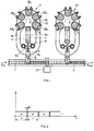
- Fig. 1 schematically shows, in a top view, a part of a manufacturing plant for inline manufacturing solar cell panels, which plant, as will be explained, may be operated to perform the method according to the invention.
- Ein solar panel substrates 1 e.g. with an extent of at least 200 mm x 200 mm, are conveyed in a stepped manner along a linear conveyor 3.
- a substrate 1 is gripped by a first transport arrangement 5 swivelably driven about an axis A 5 .
- the yet untreated substrate is transported towards a treatment facility 7.
- transport arrangement 5 transports a treated substrate from treatment facility 7 onto that position on linear conveyor 3, which has just been freed from the yet untreated substrate 1.
- the addressed treated substrate has been gripped before by the transport arrangement 5 from a further transport arrangement 9 which is swivelable about axis A 9 .
- Transport arrangement 9 is a four-armed transport arrangement. The place at the further transport arrangement 9 wherefrom the treated substrate has been gripped by transport arrangement 5 is exploited to deposit the yet untreated substrate from transport arrangement 5.
- the further transport arrangement 9 delivers a yet untreated substrate to a third transport arrangement 11 that is swivelably driven about an axis A 11 after having picked up from the addressed third transport arrangement 11, realized as a two-armed conveyor, a treated substrate.
- the third transport arrangement 11 delivers a yet untreated substrate via a loadlock arrangement 13 to a fourth transport arrangement 15 schematically shown by an arrow, after having removed a treated substrate from the addressed loadlock 13.
- the transport arrangement 15 which resides within a vacuum compartment 17 and transports, in a subsequent manner, as shown by the arrow, the substrates from one treatment station 20 a to 20 b etc., finally to the treatment station 20 e , from which the treated substrate is handed over to transport arrangement 11 via loadlock 13 so as to be conveyed towards the linear conveyor 3.
- the overall transport of substrates occurs bidirectionally as schematically shown by the double-arrows ⁇ towards and from the treatment facility 7.
- the substrates are conveyed by the transport arrangement 15 along a multitude of treatment stations as exemplified by 20 a to 20 e in an inline manner, i.e. in subsequent manner.
- the linear conveyor 3 conveys, downstream of transport arrangement 5, substrates which have been treated by the facility 7. If necessary there is provided as shown schematically at 22 a turnover station, whereat the treated substrates arriving are turned over, so that their yet untreated back surface may be treated at a further treatment facility 27. Please note that in fig. 1 treated substrate surfaces along conveyor 3 have been marked by hatching.
- the overall plant shown in fig. 1 is clocked to establish for respective time spans ⁇ of standstill, with practically neglectable dynamic phases d to move the overall plant into subsequent positions.
- fig. 2 "s" represents the standstill time span of the overall plant, whereas the short time duration d represents that time span during which there is performed dynamically forwards stepping of conveyor 3, swivelling of transport arrangements 5, 9 and 11 as well as stepping forwards from one treatment station to the next by means of transport arrangement 15 within the vacuum compartment 17.
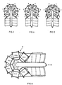
- fig. 3 there is schematically shown the treatment facility 7 as has been addressed in context with fig. 1 .
- the respective treatment stations there are marked respective surface treatments as performed according to one embodiment of the present invention.
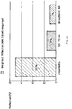
- FIG. 7 An example of treatment results of the treatment facility 7 of fig. 3 is shown in fig. 7 .
- a silicon-based substrate 30 there has been deposited a layer 32 of SiN:H with a thickness of 75 nm. This layer results from depositing at each of six subsequent treatment stations of treatment facility 7. In each of these stations a sub-layer of approx. 12.5 nm of SiN:H is deposited.
- consecutive treatment comprises first deposition of a relatively thin layer of SiN:H, followed by deposition of a relatively thick layer of SiN.
- first addressed of the consecutive treatments is performed in one single first treatment station, whereas deposition of the relatively thick layer, as the second of the consecutive treatment steps, is performed by depositing in each of the remaining five treatment stations.
- the treatment duration in each of the six subsequent treatment stations is ⁇ .
- the thickness of the deposited SiN layer is approx. 5 times the thickness of the SiN:H layer.
- manufacturing with the treatment facility 7 conceived according to fig. 4 results in a layer stack as shown in fig. 8 .
- a first layer 34 of SiN:H is deposited with a thickness of about 15 nm. This layer is deposited by the first of the six subsequent treatment stations.
- a layer of SiN is deposited with a thickness of about 60 nm. Therefrom, it might be seen that during the time span ⁇ slightly more SiN:H is deposited than during the addressed time span ⁇ in each of the five subsequent treatment stations for SiN.
- the deposition rate in the subsequent treatment stations may be adjusted so as to result in respective layers with a desired thickness, taken the boundary condition of e.g. one station for SiN:H deposition and five stations for SiN deposition, and that all stations are operative during an equal time span ⁇ .
- the layer structure as shown in fig. 8 is an improved antireflex coating stack of double-layer SiN:H/SiN.
- the SiN:H layer leads to a passivation of the silicon substrate surface, which is advantageous for an antireflex coating which is e.g. provided between the silicon-based substrate and a subsequent glass cover (not shown) .
- a relatively thin layer of SiN:H is deposited in one first of the subsequent treatment stations, then a layer of ZnS-SiO 2 .
- the layer of ZnS-SiO 2 is relatively thick, thicker than the first deposited layer of SiN:H, although deposition of both layers being performed during the same time span ⁇ . This is due to the higher deposition rate for ZnS-SiO 2 than for SiN:H.
- a layer stack which results from manufacturing the solar cell panel with the treatment facility 7 conceived as shown in fig. 5 is exemplified in fig. 9 .
- a first layer 38 of SiN:H is deposited during the time span ⁇ with a thickness of 10 nm.
- a layer 40 of ZnS-SiO 2 is deposited again during time span ⁇ and with a thickness of 60 nm.
- the respective deposition rates on one hand in the treatment station for SiN:H deposition, in the treatment station for ZnS-SiO 2 deposition and finally in the four subsequent treatment stations for deposition of SiO 2 may be respectively adjusted to cope with the boundary conditions of the respective numbers of treatment stations available on one hand and with the common treatment duration ⁇ in all treatment stations.
- the embodiment shown in fig. 9 and manufactured by the conception shown in fig. 5 is a broadband antireflex coating stack.
- the underlying SiN:H provides for surface passivation of the silicon surface.
- the spectrum (c) is shown as it results from the layer structure as shown in fig. 9 .
- a layer structure as a transparent conductive oxide layer structure e.g. of ITO, ITO:H upon the layer structure as shown in the figs. 7, 8 and 9 .
- a partial TCO Transparent Conductive Oxide
- the addressed TCO may thereby be optimized for antireflex effect, for passivation and for electrically contacting the surface of the substrate.
- a "gridless cell” or a “wider front-grid” may be realized, thereby increasing light trapping and increasing cell- and thus panel-efficiency.
- n n 1 ⁇ n 2 1 / 2
- fig. 10 there is shown in a representation in analogy to those of the figs. 3 - 5 an embodiment of the treatment facility 7 in which, in a first of the subsequent treatment stations, SiN is deposited and in the subsequent five treatment stations aluminum.
- the embodiment of the treatment facility 7 may accord with the treatment facility 27, whereat and with respect to previous treatments as performed with facility 7, the substrate has been turned over by turnover station 22 and thus the backside of the substrate is respectively treated.
- this treatment station may be conceived to deposit SiC or SiO 2 .
- a respective layer stack on the backside of the silicon-based substrate 30 is shown in fig. 11 .
- the embodiment as shown in fig. 11 manufactured by the conception as shown in fig. 10 results in a combination of a dielectric film as of SiN, SiC, SiO 2 , a-Si for backside reflexion with Al backside coating.
- the advantage gained thereby is multireflexion within the Si substrate, which leads to a total absorption of long-wavelength components of the solar light spectrum.
- contacting the backside coating may be established by (partial) laser firing (LFCs-Laser Fired Contacts).
- subdividing the consecutive treatments in fact in sub-steps, which are performed subsequently in the respective subsequent treatment stations, is performed taking into consideration the respective treatment rates of the respectively performed treatments.
- This approach most flexibly allows to industrially manufacture layer stacks with a high diversity of layer materials and thicknesses.
- Fig. 6 again shows a treatment facility 7 as has been explained in context with fig. 1 with six subsequent treatment stations, wherein, more generically, treatments PC1 to PC6 are performed in subsequent manner.
- the subsequent treatment stations as an example 6 thereof as shown in fig. 6 , may be equipped with following modules:
- Multiturn control mode offers the possibility to cycle one and the same substrate several times through at least a part of the overall manufacturing plant prior to unloading, thereby using all or some of the addressed treatment stations for different steps in building up the layer stack.
Landscapes
- Photovoltaic Devices (AREA)
- Chemical Vapour Deposition (AREA)
- Engineering & Computer Science (AREA)
- Manufacturing & Machinery (AREA)
Claims (15)
- Verfahren zur Inline-Herstellung eines Substrats, umfassend das Behandeln von Oberflächen durch aufeinanderfolgende Behandlungen unterschiedlicher Dauer, wodurch eine grundlegende Behandlungsschrittdauer festgelegt wird und jede der aufeinanderfolgenden Behandlungen unterschiedlicher Dauer in einer jeweiligen Anzahl nachfolgender Behandlungsstationen durchgeführt wird, wobei die Behandlung in allen genannten nachfolgenden Behandlungsstationen für die jeweiligen aufeinanderfolgenden Behandlungen mit einer Dauer gleich der grundlegenden Schrittdauer ist, gekennzeichnet durch die aufeinanderfolgenden Behandlungen, welche die Abscheidung einer Schicht durch ein CVD- oder PVD-Verfahren auf einem Substrat auf Siliziumbasis umfassen, wobei das Substrat durch mindestens einen Teil der nachfolgenden Behandlungsstationen schleifenförmig geführt wird.
- Verfahren nach Anspruch 1, wobei die Abscheidung einer Schicht die Abscheidung einer Schicht aus SiN:H in mehreren nachfolgenden Behandlungsstationen umfasst.
- Verfahren nach Anspruch 2, wobei die aufeinanderfolgenden Behandlungen das Abscheiden einer ersten Schicht aus SiN:H in einer ersten Anzahl nachfolgender Behandlungsstationen und das Abscheiden einer zweiten Schicht aus SiN auf der ersten Schicht in einer zweiten Anzahl nachfolgender Behandlungsstationen umfassen.
- Verfahren nach Anspruch 3, wobei die zweite Zahl so ausgewählt wird, dass sie größer als die erste Zahl ist, vorzugsweise um den Faktor 5.
- Verfahren nach Anspruch 1, wobei die aufeinanderfolgenden Behandlungen das Abscheiden einer ersten Schicht aus SiN:H in einer ersten Anzahl von nachfolgenden Behandlungsstationen, darauf eine zweite Schicht aus ZnS-SiO2 in einer zweiten Anzahl von nachfolgenden Behandlungsstationen, und darauf eine dritte Schicht aus SiO2 in einer dritten Anzahl nachfolgender Behandlungsstationen umfassen.
- Verfahren nach Anspruch 5, wobei die erste und die zweite Zahl gleich gewählt wird.
- Verfahren nach einem der Ansprüche 5 oder 6, wobei die dritte Zahl größer als die erste Zahl gewählt wird, vorzugsweise um den Faktor 4.
- Verfahren nach Anspruch 1, wobei die aufeinanderfolgenden Behandlungen die Abscheidung einer Schicht aus einem der folgenden Materialien umfassen: Al, AlN, Al2O3, ITO, ITO:H, CrO2, GeN, SiC, SiON, SiO2, SiAlON, SiNiON, TiO2, ZAO (zinkaluminumoxid), MgF2, ZNO, Ag, Au, AuSn, AuGe, Cu, Cr, Ni, NiV, Ti, a-Si, SiGe, ZnS, SiN:H, SiN.
- Verfahren nach Anspruch 1, wobei die aufeinanderfolgenden Behandlungen mindestens eine der Folgenden umfassen:• PVD-Sputtern von einer Quelle• PVD-Sputtern von mehreren Quellen• PECVD• LEPCVD• Ätzen• Kühlen• Entgasen.
- Verfahren nach Anspruch 1, wobei das Substrat durch mindestens einen Teil der nachfolgenden Behandlungsstationen mehr als einmal schleifenförmig geführt wird.
- Verfahren nach Anspruch 1, wobei die aufeinanderfolgenden Behandlungen das Abscheiden von Schichten auf beiden Seiten eines Substrats umfassen.
- Verfahren nach Anspruch 11, wobei die Schichten aus einer ersten Schicht aus SiN, SiC, SiO2 oder a-Si und einer zweiten Schicht aus Al oder Ag bestehen.
- Verfahren nach Anspruch 12, wobei die erste Schicht aus SiN in einer ersten Anzahl nachfolgender Behandlungsstationen abgeschieden wird, die zweite Schicht aus Al in einer zweiten Anzahl nachfolgender Behandlungsstationen abgeschieden wird, wobei die zweite Anzahl größer als die erste Zahl gewählt wird, vorzugsweise um den Faktor 5.
- Verfahren nach einem der vorhergehenden Ansprüche, dadurch gekennzeichnet, dass es die Verwendung einer Produktionsanlage umfasst, die zu Folgendem ausgelegt ist:- lineares Fördern des Substrats mit den zu behandelnden Oberflächen und anschließendes Verzweigen der Substrate von dem linearen Fördern und Fördern in Richtung der jeweiligen Anzahl nachfolgender Behandlungsstationen, wobei eine rotierende Fördern der Substrate zwischen den Behandlungsstationen durch eine Rotationsförderung und ein erneutes Aufbringen der in den Behandlungsstationen behandelten Substrate zur linearen Förderung erfolgt.
- Produktionsanlage, umfassend einen linearen Förderer (3), eine Transportanordnung (5, 9, 11), eine Ladeschleusenanordnung (13) und in einem Vakuumraum (17) eine Rotationstransportanordnung (15) und nachfolgende Behandlungsstationen (20a, 20b, 20c, 20d, 20e), die dazu ausgelegt sind das folgende Verfahren auszuführen:- Behandeln von Oberflächen von Substraten durch aufeinanderfolgende Behandlungen unterschiedlicher Dauer, wodurch eine grundlegende Behandlungsschrittdauer festgelegt wird und- Durchführen jeder der aufeinanderfolgenden Behandlungen unterschiedlicher Dauer in einer jeweiligen Anzahl nachfolgender Behandlungsstationen (20a, 20b, 20c, 20d, 20e), Behandlung in allen nachfolgenden Behandlungsstationen (20a, 20b, 20c, 20d, 20e) wobei die jeweiligen aufeinanderfolgenden Behandlungen eine Dauer haben, die gleich der grundlegenden Schrittdauer ist,- lineares Fördern von Substraten mit den zu behandelnden Oberflächen und anschließendes Verzweigen der Substrate von dem linearen Förderer (3) und Fördern zu der jeweiligen Anzahl nachfolgender Behandlungsstationen (20a, 20b, 20c, 20d, 20e) über eine Ladeschleuse (13), wobei ein Rotieren der Substrate zwischen den Behandlungsstationen (20a, 20b, 20c, 20d, 20e) durch eine Rotationstransportanordnung (15) und ein erneutes Aufbringen von Substraten, die in den Behandlungsstationen (20a, 20b, 20c, 20d, 20e) behandelt wurden, über eine Ladeschleuse (13) und Transportanordnung (5, 9, 11) zu dem linearen Förderer (3) erfolgt;- die Rotationstransportanordnung 15 dazu konfiguriert ist, um die Substrate durch mindestens einen Teil der nachfolgenden Behandlungsstationen schleifenförmig zu führen.
Applications Claiming Priority (4)
| Application Number | Priority Date | Filing Date | Title |
|---|---|---|---|
| US16108409P | 2009-03-18 | 2009-03-18 | |
| US16393909P | 2009-03-27 | 2009-03-27 | |
| EP10710271.7A EP2409339B1 (de) | 2009-03-18 | 2010-03-15 | Verfahren zur schrittweisen herstellung einer solarzellentafel |
| PCT/EP2010/053273 WO2010106012A2 (en) | 2009-03-18 | 2010-03-15 | Method of inline manufacturing a solar cell panel |
Related Parent Applications (2)
| Application Number | Title | Priority Date | Filing Date |
|---|---|---|---|
| EP10710271.7A Division EP2409339B1 (de) | 2009-03-18 | 2010-03-15 | Verfahren zur schrittweisen herstellung einer solarzellentafel |
| EP10710271.7A Division-Into EP2409339B1 (de) | 2009-03-18 | 2010-03-15 | Verfahren zur schrittweisen herstellung einer solarzellentafel |
Publications (2)
| Publication Number | Publication Date |
|---|---|
| EP3249699A1 EP3249699A1 (de) | 2017-11-29 |
| EP3249699B1 true EP3249699B1 (de) | 2020-04-15 |
Family
ID=42740049
Family Applications (2)
| Application Number | Title | Priority Date | Filing Date |
|---|---|---|---|
| EP17178806.0A Not-in-force EP3249699B1 (de) | 2009-03-18 | 2010-03-15 | Verfahren zur inline-herstellung einer solarzellentafel |
| EP10710271.7A Not-in-force EP2409339B1 (de) | 2009-03-18 | 2010-03-15 | Verfahren zur schrittweisen herstellung einer solarzellentafel |
Family Applications After (1)
| Application Number | Title | Priority Date | Filing Date |
|---|---|---|---|
| EP10710271.7A Not-in-force EP2409339B1 (de) | 2009-03-18 | 2010-03-15 | Verfahren zur schrittweisen herstellung einer solarzellentafel |
Country Status (7)
| Country | Link |
|---|---|
| US (1) | US9214589B2 (de) |
| EP (2) | EP3249699B1 (de) |
| KR (2) | KR101632646B1 (de) |
| CN (1) | CN102388467B (de) |
| SG (1) | SG10201400525UA (de) |
| TW (1) | TWI501408B (de) |
| WO (1) | WO2010106012A2 (de) |
Families Citing this family (19)
| Publication number | Priority date | Publication date | Assignee | Title |
|---|---|---|---|---|
| CN102881763A (zh) * | 2011-07-11 | 2013-01-16 | 刘莹 | 一种激光烧结制晶体硅太阳能电池背电极的设备 |
| DE102011084644A1 (de) * | 2011-10-17 | 2013-04-18 | Osram Gmbh | Verfahren zur herstellung eines photovoltaischen elements mit einer siliziumdioxidschicht |
| KR20160104750A (ko) * | 2012-08-07 | 2016-09-05 | 요코하마 고무 가부시키가이샤 | 공기입 타이어 |
| US10518582B2 (en) * | 2012-10-10 | 2019-12-31 | The Yokohama Rubber Co., Ltd. | Pneumatic tire |
| EP3069189A1 (de) | 2013-11-14 | 2016-09-21 | Oerlikon Advanced Technologies AG | Vorrichtung und verfahren zum tempern von beschichtungen zum schutz vor fingerabdrücken |
| CN106549065A (zh) * | 2016-10-24 | 2017-03-29 | 苏州阿特斯阳光电力科技有限公司 | 一种低反射率膜层结构 |
| WO2019020391A1 (en) | 2017-07-27 | 2019-01-31 | Evatec Ag | Permeation-barrier |
| US10998209B2 (en) | 2019-05-31 | 2021-05-04 | Applied Materials, Inc. | Substrate processing platforms including multiple processing chambers |
| US12080571B2 (en) | 2020-07-08 | 2024-09-03 | Applied Materials, Inc. | Substrate processing module and method of moving a workpiece |
| US11817331B2 (en) | 2020-07-27 | 2023-11-14 | Applied Materials, Inc. | Substrate holder replacement with protective disk during pasting process |
| US11749542B2 (en) | 2020-07-27 | 2023-09-05 | Applied Materials, Inc. | Apparatus, system, and method for non-contact temperature monitoring of substrate supports |
| US11600507B2 (en) | 2020-09-09 | 2023-03-07 | Applied Materials, Inc. | Pedestal assembly for a substrate processing chamber |
| US11610799B2 (en) | 2020-09-18 | 2023-03-21 | Applied Materials, Inc. | Electrostatic chuck having a heating and chucking capabilities |
| US12195314B2 (en) | 2021-02-02 | 2025-01-14 | Applied Materials, Inc. | Cathode exchange mechanism to improve preventative maintenance time for cluster system |
| US11674227B2 (en) | 2021-02-03 | 2023-06-13 | Applied Materials, Inc. | Symmetric pump down mini-volume with laminar flow cavity gas injection for high and low pressure |
| KR102514021B1 (ko) | 2021-03-18 | 2023-03-24 | 고려대학교 산학협력단 | 투명 복사 냉각 소자 |
| US12002668B2 (en) | 2021-06-25 | 2024-06-04 | Applied Materials, Inc. | Thermal management hardware for uniform temperature control for enhanced bake-out for cluster tool |
| KR102596161B1 (ko) | 2021-09-13 | 2023-10-31 | 고려대학교 산학협력단 | 투명 복사 냉각 소자 |
| DE102022116340B4 (de) | 2022-06-30 | 2024-12-19 | VON ARDENNE Asset GmbH & Co. KG | Verfahren und Solarzelle |
Family Cites Families (24)
| Publication number | Priority date | Publication date | Assignee | Title |
|---|---|---|---|---|
| TW276353B (de) * | 1993-07-15 | 1996-05-21 | Hitachi Seisakusyo Kk | |
| EP1228538A1 (de) * | 1999-10-13 | 2002-08-07 | Universität Konstanz | Verfahren und vorrichtung zur herstellung von solarzellen |
| US6423565B1 (en) * | 2000-05-30 | 2002-07-23 | Kurt L. Barth | Apparatus and processes for the massproduction of photovotaic modules |
| US20090004850A1 (en) * | 2001-07-25 | 2009-01-01 | Seshadri Ganguli | Process for forming cobalt and cobalt silicide materials in tungsten contact applications |
| EP1751805A4 (de) * | 2004-04-30 | 2007-07-04 | Newsouth Innovations Pty Ltd | Künstliche amorphe halbleiter und anwendungen auf solarzellen |
| KR100823216B1 (ko) * | 2004-05-17 | 2008-04-21 | 가부시키가이샤 히다치 고쿠사이 덴키 | 기판 처리 장치 및 반도체 디바이스 제조 방법 |
| WO2006057319A1 (ja) * | 2004-11-24 | 2006-06-01 | Hitachi Kokusai Electric Inc. | 基板処理装置 |
| US8078311B2 (en) * | 2004-12-06 | 2011-12-13 | Tokyo Electron Limited | Substrate processing apparatus and substrate transfer method adopted in substrate processing apparatus |
| US7361585B2 (en) * | 2004-12-23 | 2008-04-22 | Advantech Global, Ltd | System for and method of planarizing the contact region of a via by use of a continuous inline vacuum deposition |
| US20070017445A1 (en) * | 2005-07-19 | 2007-01-25 | Takako Takehara | Hybrid PVD-CVD system |
| US7973379B2 (en) * | 2005-12-26 | 2011-07-05 | Citizen Holdings Co., Ltd. | Photovoltaic ultraviolet sensor |
| CN101495671A (zh) * | 2006-04-11 | 2009-07-29 | 应用材料公司 | 用于形成太阳能电池板的系统结构及其方法 |
| US20070254112A1 (en) * | 2006-04-26 | 2007-11-01 | Applied Materials, Inc. | Apparatus and method for high utilization of process chambers of a cluster system through staggered plasma cleaning |
| KR100818044B1 (ko) * | 2006-05-04 | 2008-03-31 | 위순임 | 기판 지지대와 기판 반송 장치 및 이를 이용한 기판 처리시스템 |
| WO2008106812A1 (en) * | 2007-03-02 | 2008-09-12 | Oerlikon Trading Ag, Trübbach | Vacuum coating apparatus |
| EP1976022A3 (de) * | 2007-03-29 | 2008-12-03 | Applied Materials, Inc. | Verfahren und Vorrichtung zur Herstellung einer Antireflexionsschicht oder einer Passivierungsschicht für Solarzellen |
| US20080302653A1 (en) | 2007-03-29 | 2008-12-11 | Applied Materials Inc. | Method And Device For Producing An Anti-Reflection Or Passivation Layer For Solar Cells |
| US20080271675A1 (en) * | 2007-05-01 | 2008-11-06 | Applied Materials, Inc. | Method of forming thin film solar cells |
| US8114484B2 (en) * | 2007-07-19 | 2012-02-14 | Applied Materials, Inc. | Plasma enhanced chemical vapor deposition technology for large-size processing |
| US7763535B2 (en) * | 2007-08-30 | 2010-07-27 | Applied Materials, Inc. | Method for producing a metal backside contact of a semiconductor component, in particular, a solar cell |
| KR20100046163A (ko) * | 2007-08-30 | 2010-05-06 | 어플라이드 머티어리얼스, 인코포레이티드 | 반도체 소자, 특히 태양 전지의 금속 후면 접점의 제조 방법 |
| US7588957B2 (en) * | 2007-10-17 | 2009-09-15 | Applied Materials, Inc. | CVD process gas flow, pumping and/or boosting |
| US20090197015A1 (en) * | 2007-12-25 | 2009-08-06 | Applied Materials, Inc. | Method and apparatus for controlling plasma uniformity |
| JP4707749B2 (ja) * | 2009-04-01 | 2011-06-22 | 東京エレクトロン株式会社 | 基板交換方法及び基板処理装置 |
-
2010
- 2010-03-15 EP EP17178806.0A patent/EP3249699B1/de not_active Not-in-force
- 2010-03-15 EP EP10710271.7A patent/EP2409339B1/de not_active Not-in-force
- 2010-03-15 US US13/256,979 patent/US9214589B2/en active Active
- 2010-03-15 WO PCT/EP2010/053273 patent/WO2010106012A2/en not_active Ceased
- 2010-03-15 KR KR1020117024382A patent/KR101632646B1/ko not_active Expired - Fee Related
- 2010-03-15 SG SG10201400525UA patent/SG10201400525UA/en unknown
- 2010-03-15 KR KR1020167015825A patent/KR101717409B1/ko not_active Expired - Fee Related
- 2010-03-15 CN CN201080012883.8A patent/CN102388467B/zh not_active Expired - Fee Related
- 2010-03-16 TW TW099107571A patent/TWI501408B/zh not_active IP Right Cessation
Non-Patent Citations (1)
| Title |
|---|
| None * |
Also Published As
| Publication number | Publication date |
|---|---|
| KR101632646B1 (ko) | 2016-07-01 |
| CN102388467A (zh) | 2012-03-21 |
| TW201114042A (en) | 2011-04-16 |
| KR20110138243A (ko) | 2011-12-26 |
| WO2010106012A3 (en) | 2011-06-03 |
| TWI501408B (zh) | 2015-09-21 |
| SG10201400525UA (en) | 2014-05-29 |
| WO2010106012A2 (en) | 2010-09-23 |
| KR101717409B1 (ko) | 2017-03-16 |
| CN102388467B (zh) | 2015-05-13 |
| US9214589B2 (en) | 2015-12-15 |
| US20120009730A1 (en) | 2012-01-12 |
| KR20160075821A (ko) | 2016-06-29 |
| EP2409339B1 (de) | 2017-09-06 |
| EP2409339A2 (de) | 2012-01-25 |
| EP3249699A1 (de) | 2017-11-29 |
Similar Documents
| Publication | Publication Date | Title |
|---|---|---|
| EP2409339B1 (de) | Verfahren zur schrittweisen herstellung einer solarzellentafel | |
| EP1424735B1 (de) | Verfahren zur ausbildung einer lichtabsorbierenden schicht | |
| US8021905B1 (en) | Machine and process for sequential multi-sublayer deposition of copper indium gallium diselenide compound semiconductors | |
| TW201336098A (zh) | 鈍化矽晶太陽能電池的先進平台 | |
| WO2011130017A2 (en) | Multi-layer sin for functional and optical graded arc layers on crystalline solar cells | |
| EP2232556A1 (de) | Systeme und verfahren zur parallelschaltung von fotovoltaikmodulen | |
| US20050095809A1 (en) | Method of film-forming transparent electrode layer and device therefor | |
| CN118630101A (zh) | 一种晶硅基电池片分片断面的钝化修复方法及钝化装置 | |
| WO2010023991A1 (ja) | 光電変換装置の製造方法、光電変換装置、及び光電変換装置の製造システム | |
| JP3787410B2 (ja) | 堆積膜製造方法及び光起電力素子の製造方法 | |
| JP2010537439A (ja) | 半導体構成要素、特にソーラーセルの金属裏側コンタクトの製造方法 | |
| US20170236710A1 (en) | Machine and process for continuous, sequential, deposition of semiconductor solar absorbers having variable semiconductor composition deposited in multiple sublayers | |
| AU2006310865B2 (en) | Antireflective coating on solar cells and method for the production of such an antireflective coating | |
| CN115101446A (zh) | Pvd镀膜设备和异质结电池的镀膜方法 | |
| US20110092079A1 (en) | Method and installation for producing an anti-reflection and/or passivation coating for semiconductor devices | |
| KR20100046163A (ko) | 반도체 소자, 특히 태양 전지의 금속 후면 접점의 제조 방법 | |
| CN100380592C (zh) | 薄膜形成装置、薄膜形成方法和薄膜形成系统 | |
| CN120419320A (zh) | 制造太阳能电池的方法 | |
| US20120034731A1 (en) | Photoelectric conversion device manufacturing system and photoelectric conversion device manufacturing method | |
| WO2010023948A1 (ja) | 光電変換装置の製造方法、光電変換装置、及び光電変換装置の製造システム | |
| KR20170052147A (ko) | 기판처리시스템 및 기판처리방법 | |
| JPH04242979A (ja) | 薄膜半導体装置製造装置 |
Legal Events
| Date | Code | Title | Description |
|---|---|---|---|
| PUAI | Public reference made under article 153(3) epc to a published international application that has entered the european phase |
Free format text: ORIGINAL CODE: 0009012 |
|
| STAA | Information on the status of an ep patent application or granted ep patent |
Free format text: STATUS: THE APPLICATION HAS BEEN PUBLISHED |
|
| AC | Divisional application: reference to earlier application |
Ref document number: 2409339 Country of ref document: EP Kind code of ref document: P |
|
| AK | Designated contracting states |
Kind code of ref document: A1 Designated state(s): AT BE BG CH CY CZ DE DK EE ES FI FR GB GR HR HU IE IS IT LI LT LU LV MC MK MT NL NO PL PT RO SE SI SK SM TR |
|
| RIN1 | Information on inventor provided before grant (corrected) |
Inventor name: WUESTENHAGEN, VOLKER Inventor name: DOVIDS, GERHARD Inventor name: VOSER, STEPHAN Inventor name: FEISTRITZER, GERALD Inventor name: RATTUNDE, OLIVER DR. Inventor name: DUBS, MARTIN |
|
| RAP1 | Party data changed (applicant data changed or rights of an application transferred) |
Owner name: EVATEC AG |
|
| STAA | Information on the status of an ep patent application or granted ep patent |
Free format text: STATUS: REQUEST FOR EXAMINATION WAS MADE |
|
| 17P | Request for examination filed |
Effective date: 20180413 |
|
| RBV | Designated contracting states (corrected) |
Designated state(s): AT BE BG CH CY CZ DE DK EE ES FI FR GB GR HR HU IE IS IT LI LT LU LV MC MK MT NL NO PL PT RO SE SI SK SM TR |
|
| GRAP | Despatch of communication of intention to grant a patent |
Free format text: ORIGINAL CODE: EPIDOSNIGR1 |
|
| STAA | Information on the status of an ep patent application or granted ep patent |
Free format text: STATUS: GRANT OF PATENT IS INTENDED |
|
| INTG | Intention to grant announced |
Effective date: 20191112 |
|
| GRAS | Grant fee paid |
Free format text: ORIGINAL CODE: EPIDOSNIGR3 |
|
| GRAA | (expected) grant |
Free format text: ORIGINAL CODE: 0009210 |
|
| STAA | Information on the status of an ep patent application or granted ep patent |
Free format text: STATUS: THE PATENT HAS BEEN GRANTED |
|
| AC | Divisional application: reference to earlier application |
Ref document number: 2409339 Country of ref document: EP Kind code of ref document: P |
|
| AK | Designated contracting states |
Kind code of ref document: B1 Designated state(s): AT BE BG CH CY CZ DE DK EE ES FI FR GB GR HR HU IE IS IT LI LT LU LV MC MK MT NL NO PL PT RO SE SI SK SM TR |
|
| REG | Reference to a national code |
Ref country code: CH Ref legal event code: EP |
|
| REG | Reference to a national code |
Ref country code: DE Ref legal event code: R096 Ref document number: 602010063968 Country of ref document: DE |
|
| REG | Reference to a national code |
Ref country code: IE Ref legal event code: FG4D |
|
| REG | Reference to a national code |
Ref country code: CH Ref legal event code: NV Representative=s name: TROESCH SCHEIDEGGER WERNER AG, CH Ref country code: AT Ref legal event code: REF Ref document number: 1258312 Country of ref document: AT Kind code of ref document: T Effective date: 20200515 |
|
| REG | Reference to a national code |
Ref country code: NL Ref legal event code: MP Effective date: 20200415 |
|
| REG | Reference to a national code |
Ref country code: LT Ref legal event code: MG4D |
|
| PG25 | Lapsed in a contracting state [announced via postgrant information from national office to epo] |
Ref country code: SE Free format text: LAPSE BECAUSE OF FAILURE TO SUBMIT A TRANSLATION OF THE DESCRIPTION OR TO PAY THE FEE WITHIN THE PRESCRIBED TIME-LIMIT Effective date: 20200415 Ref country code: NL Free format text: LAPSE BECAUSE OF FAILURE TO SUBMIT A TRANSLATION OF THE DESCRIPTION OR TO PAY THE FEE WITHIN THE PRESCRIBED TIME-LIMIT Effective date: 20200415 Ref country code: LT Free format text: LAPSE BECAUSE OF FAILURE TO SUBMIT A TRANSLATION OF THE DESCRIPTION OR TO PAY THE FEE WITHIN THE PRESCRIBED TIME-LIMIT Effective date: 20200415 Ref country code: GR Free format text: LAPSE BECAUSE OF FAILURE TO SUBMIT A TRANSLATION OF THE DESCRIPTION OR TO PAY THE FEE WITHIN THE PRESCRIBED TIME-LIMIT Effective date: 20200716 Ref country code: FI Free format text: LAPSE BECAUSE OF FAILURE TO SUBMIT A TRANSLATION OF THE DESCRIPTION OR TO PAY THE FEE WITHIN THE PRESCRIBED TIME-LIMIT Effective date: 20200415 Ref country code: PT Free format text: LAPSE BECAUSE OF FAILURE TO SUBMIT A TRANSLATION OF THE DESCRIPTION OR TO PAY THE FEE WITHIN THE PRESCRIBED TIME-LIMIT Effective date: 20200817 Ref country code: NO Free format text: LAPSE BECAUSE OF FAILURE TO SUBMIT A TRANSLATION OF THE DESCRIPTION OR TO PAY THE FEE WITHIN THE PRESCRIBED TIME-LIMIT Effective date: 20200715 Ref country code: IS Free format text: LAPSE BECAUSE OF FAILURE TO SUBMIT A TRANSLATION OF THE DESCRIPTION OR TO PAY THE FEE WITHIN THE PRESCRIBED TIME-LIMIT Effective date: 20200815 |
|
| REG | Reference to a national code |
Ref country code: AT Ref legal event code: MK05 Ref document number: 1258312 Country of ref document: AT Kind code of ref document: T Effective date: 20200415 |
|
| PG25 | Lapsed in a contracting state [announced via postgrant information from national office to epo] |
Ref country code: HR Free format text: LAPSE BECAUSE OF FAILURE TO SUBMIT A TRANSLATION OF THE DESCRIPTION OR TO PAY THE FEE WITHIN THE PRESCRIBED TIME-LIMIT Effective date: 20200415 Ref country code: LV Free format text: LAPSE BECAUSE OF FAILURE TO SUBMIT A TRANSLATION OF THE DESCRIPTION OR TO PAY THE FEE WITHIN THE PRESCRIBED TIME-LIMIT Effective date: 20200415 Ref country code: BG Free format text: LAPSE BECAUSE OF FAILURE TO SUBMIT A TRANSLATION OF THE DESCRIPTION OR TO PAY THE FEE WITHIN THE PRESCRIBED TIME-LIMIT Effective date: 20200715 |
|
| REG | Reference to a national code |
Ref country code: DE Ref legal event code: R097 Ref document number: 602010063968 Country of ref document: DE |
|
| PG25 | Lapsed in a contracting state [announced via postgrant information from national office to epo] |
Ref country code: RO Free format text: LAPSE BECAUSE OF FAILURE TO SUBMIT A TRANSLATION OF THE DESCRIPTION OR TO PAY THE FEE WITHIN THE PRESCRIBED TIME-LIMIT Effective date: 20200415 Ref country code: ES Free format text: LAPSE BECAUSE OF FAILURE TO SUBMIT A TRANSLATION OF THE DESCRIPTION OR TO PAY THE FEE WITHIN THE PRESCRIBED TIME-LIMIT Effective date: 20200415 Ref country code: CZ Free format text: LAPSE BECAUSE OF FAILURE TO SUBMIT A TRANSLATION OF THE DESCRIPTION OR TO PAY THE FEE WITHIN THE PRESCRIBED TIME-LIMIT Effective date: 20200415 Ref country code: AT Free format text: LAPSE BECAUSE OF FAILURE TO SUBMIT A TRANSLATION OF THE DESCRIPTION OR TO PAY THE FEE WITHIN THE PRESCRIBED TIME-LIMIT Effective date: 20200415 Ref country code: DK Free format text: LAPSE BECAUSE OF FAILURE TO SUBMIT A TRANSLATION OF THE DESCRIPTION OR TO PAY THE FEE WITHIN THE PRESCRIBED TIME-LIMIT Effective date: 20200415 Ref country code: EE Free format text: LAPSE BECAUSE OF FAILURE TO SUBMIT A TRANSLATION OF THE DESCRIPTION OR TO PAY THE FEE WITHIN THE PRESCRIBED TIME-LIMIT Effective date: 20200415 Ref country code: IT Free format text: LAPSE BECAUSE OF FAILURE TO SUBMIT A TRANSLATION OF THE DESCRIPTION OR TO PAY THE FEE WITHIN THE PRESCRIBED TIME-LIMIT Effective date: 20200415 Ref country code: SM Free format text: LAPSE BECAUSE OF FAILURE TO SUBMIT A TRANSLATION OF THE DESCRIPTION OR TO PAY THE FEE WITHIN THE PRESCRIBED TIME-LIMIT Effective date: 20200415 |
|
| PLBE | No opposition filed within time limit |
Free format text: ORIGINAL CODE: 0009261 |
|
| STAA | Information on the status of an ep patent application or granted ep patent |
Free format text: STATUS: NO OPPOSITION FILED WITHIN TIME LIMIT |
|
| PG25 | Lapsed in a contracting state [announced via postgrant information from national office to epo] |
Ref country code: PL Free format text: LAPSE BECAUSE OF FAILURE TO SUBMIT A TRANSLATION OF THE DESCRIPTION OR TO PAY THE FEE WITHIN THE PRESCRIBED TIME-LIMIT Effective date: 20200415 Ref country code: SK Free format text: LAPSE BECAUSE OF FAILURE TO SUBMIT A TRANSLATION OF THE DESCRIPTION OR TO PAY THE FEE WITHIN THE PRESCRIBED TIME-LIMIT Effective date: 20200415 |
|
| 26N | No opposition filed |
Effective date: 20210118 |
|
| PGFP | Annual fee paid to national office [announced via postgrant information from national office to epo] |
Ref country code: FR Payment date: 20210210 Year of fee payment: 12 |
|
| PG25 | Lapsed in a contracting state [announced via postgrant information from national office to epo] |
Ref country code: SI Free format text: LAPSE BECAUSE OF FAILURE TO SUBMIT A TRANSLATION OF THE DESCRIPTION OR TO PAY THE FEE WITHIN THE PRESCRIBED TIME-LIMIT Effective date: 20200415 |
|
| PGFP | Annual fee paid to national office [announced via postgrant information from national office to epo] |
Ref country code: GB Payment date: 20210308 Year of fee payment: 12 |
|
| PG25 | Lapsed in a contracting state [announced via postgrant information from national office to epo] |
Ref country code: MC Free format text: LAPSE BECAUSE OF FAILURE TO SUBMIT A TRANSLATION OF THE DESCRIPTION OR TO PAY THE FEE WITHIN THE PRESCRIBED TIME-LIMIT Effective date: 20200415 |
|
| REG | Reference to a national code |
Ref country code: CH Ref legal event code: PL |
|
| REG | Reference to a national code |
Ref country code: BE Ref legal event code: MM Effective date: 20210331 |
|
| PG25 | Lapsed in a contracting state [announced via postgrant information from national office to epo] |
Ref country code: IE Free format text: LAPSE BECAUSE OF NON-PAYMENT OF DUE FEES Effective date: 20210315 Ref country code: CH Free format text: LAPSE BECAUSE OF NON-PAYMENT OF DUE FEES Effective date: 20210331 Ref country code: LI Free format text: LAPSE BECAUSE OF NON-PAYMENT OF DUE FEES Effective date: 20210331 Ref country code: LU Free format text: LAPSE BECAUSE OF NON-PAYMENT OF DUE FEES Effective date: 20210315 |
|
| PG25 | Lapsed in a contracting state [announced via postgrant information from national office to epo] |
Ref country code: BE Free format text: LAPSE BECAUSE OF NON-PAYMENT OF DUE FEES Effective date: 20210331 |
|
| GBPC | Gb: european patent ceased through non-payment of renewal fee |
Effective date: 20220315 |
|
| PG25 | Lapsed in a contracting state [announced via postgrant information from national office to epo] |
Ref country code: GB Free format text: LAPSE BECAUSE OF NON-PAYMENT OF DUE FEES Effective date: 20220315 Ref country code: FR Free format text: LAPSE BECAUSE OF NON-PAYMENT OF DUE FEES Effective date: 20220331 |
|
| REG | Reference to a national code |
Ref country code: DE Ref legal event code: R082 Ref document number: 602010063968 Country of ref document: DE Representative=s name: SKM-IP SCHMID KRAUSS KUTTENKEULER MALESCHA SCH, DE |
|
| PG25 | Lapsed in a contracting state [announced via postgrant information from national office to epo] |
Ref country code: CY Free format text: LAPSE BECAUSE OF FAILURE TO SUBMIT A TRANSLATION OF THE DESCRIPTION OR TO PAY THE FEE WITHIN THE PRESCRIBED TIME-LIMIT Effective date: 20200415 |
|
| P01 | Opt-out of the competence of the unified patent court (upc) registered |
Effective date: 20230526 |
|
| PG25 | Lapsed in a contracting state [announced via postgrant information from national office to epo] |
Ref country code: HU Free format text: LAPSE BECAUSE OF FAILURE TO SUBMIT A TRANSLATION OF THE DESCRIPTION OR TO PAY THE FEE WITHIN THE PRESCRIBED TIME-LIMIT; INVALID AB INITIO Effective date: 20100315 |
|
| PG25 | Lapsed in a contracting state [announced via postgrant information from national office to epo] |
Ref country code: MK Free format text: LAPSE BECAUSE OF FAILURE TO SUBMIT A TRANSLATION OF THE DESCRIPTION OR TO PAY THE FEE WITHIN THE PRESCRIBED TIME-LIMIT Effective date: 20200415 |
|
| PGFP | Annual fee paid to national office [announced via postgrant information from national office to epo] |
Ref country code: DE Payment date: 20240130 Year of fee payment: 15 |
|
| PG25 | Lapsed in a contracting state [announced via postgrant information from national office to epo] |
Ref country code: TR Free format text: LAPSE BECAUSE OF FAILURE TO SUBMIT A TRANSLATION OF THE DESCRIPTION OR TO PAY THE FEE WITHIN THE PRESCRIBED TIME-LIMIT Effective date: 20200415 |
|
| PG25 | Lapsed in a contracting state [announced via postgrant information from national office to epo] |
Ref country code: MT Free format text: LAPSE BECAUSE OF FAILURE TO SUBMIT A TRANSLATION OF THE DESCRIPTION OR TO PAY THE FEE WITHIN THE PRESCRIBED TIME-LIMIT Effective date: 20200415 |
|
| REG | Reference to a national code |
Ref country code: DE Ref legal event code: R079 Ref document number: 602010063968 Country of ref document: DE Free format text: PREVIOUS MAIN CLASS: H01L0031180000 Ipc: H10F0071000000 |
|
| REG | Reference to a national code |
Ref country code: DE Ref legal event code: R119 Ref document number: 602010063968 Country of ref document: DE |
|
| PG25 | Lapsed in a contracting state [announced via postgrant information from national office to epo] |
Ref country code: DE Free format text: LAPSE BECAUSE OF NON-PAYMENT OF DUE FEES Effective date: 20251001 |