EP3205021B1 - High voltage zero qrr bootstrap supply - Google Patents
High voltage zero qrr bootstrap supply Download PDFInfo
- Publication number
- EP3205021B1 EP3205021B1 EP15848411.3A EP15848411A EP3205021B1 EP 3205021 B1 EP3205021 B1 EP 3205021B1 EP 15848411 A EP15848411 A EP 15848411A EP 3205021 B1 EP3205021 B1 EP 3205021B1
- Authority
- EP
- European Patent Office
- Prior art keywords
- bootstrap
- transistor
- gate driver
- low side
- high side
- Prior art date
- Legal status (The legal status is an assumption and is not a legal conclusion. Google has not performed a legal analysis and makes no representation as to the accuracy of the status listed.)
- Active
Links
Images

Classifications
-
- H—ELECTRICITY
- H03—ELECTRONIC CIRCUITRY
- H03K—PULSE TECHNIQUE
- H03K17/00—Electronic switching or gating, i.e. not by contact-making and –breaking
- H03K17/04—Modifications for accelerating switching
- H03K17/042—Modifications for accelerating switching by feedback from the output circuit to the control circuit
- H03K17/04206—Modifications for accelerating switching by feedback from the output circuit to the control circuit in field-effect transistor switches
-
- H—ELECTRICITY
- H03—ELECTRONIC CIRCUITRY
- H03K—PULSE TECHNIQUE
- H03K17/00—Electronic switching or gating, i.e. not by contact-making and –breaking
- H03K17/51—Electronic switching or gating, i.e. not by contact-making and –breaking characterised by the components used
- H03K17/56—Electronic switching or gating, i.e. not by contact-making and –breaking characterised by the components used by the use, as active elements, of semiconductor devices
- H03K17/567—Circuits characterised by the use of more than one type of semiconductor device, e.g. BIMOS, composite devices such as IGBT
-
- H—ELECTRICITY
- H03—ELECTRONIC CIRCUITRY
- H03K—PULSE TECHNIQUE
- H03K17/00—Electronic switching or gating, i.e. not by contact-making and –breaking
- H03K17/16—Modifications for eliminating interference voltages or currents
- H03K17/161—Modifications for eliminating interference voltages or currents in field-effect transistor switches
- H03K17/165—Modifications for eliminating interference voltages or currents in field-effect transistor switches by feedback from the output circuit to the control circuit
-
- H—ELECTRICITY
- H03—ELECTRONIC CIRCUITRY
- H03K—PULSE TECHNIQUE
- H03K17/00—Electronic switching or gating, i.e. not by contact-making and –breaking
- H03K17/51—Electronic switching or gating, i.e. not by contact-making and –breaking characterised by the components used
- H03K17/56—Electronic switching or gating, i.e. not by contact-making and –breaking characterised by the components used by the use, as active elements, of semiconductor devices
- H03K17/687—Electronic switching or gating, i.e. not by contact-making and –breaking characterised by the components used by the use, as active elements, of semiconductor devices the devices being field-effect transistors
- H03K17/6871—Electronic switching or gating, i.e. not by contact-making and –breaking characterised by the components used by the use, as active elements, of semiconductor devices the devices being field-effect transistors the output circuit comprising more than one controlled field-effect transistor
-
- H—ELECTRICITY
- H03—ELECTRONIC CIRCUITRY
- H03K—PULSE TECHNIQUE
- H03K19/00—Logic circuits, i.e. having at least two inputs acting on one output; Inverting circuits
- H03K19/0175—Coupling arrangements; Interface arrangements
- H03K19/017509—Interface arrangements
-
- H—ELECTRICITY
- H03—ELECTRONIC CIRCUITRY
- H03K—PULSE TECHNIQUE
- H03K2217/00—Indexing scheme related to electronic switching or gating, i.e. not by contact-making or -breaking covered by H03K17/00
- H03K2217/0063—High side switches, i.e. the higher potential [DC] or life wire [AC] being directly connected to the switch and not via the load
-
- H—ELECTRICITY
- H03—ELECTRONIC CIRCUITRY
- H03K—PULSE TECHNIQUE
- H03K2217/00—Indexing scheme related to electronic switching or gating, i.e. not by contact-making or -breaking covered by H03K17/00
- H03K2217/0072—Low side switches, i.e. the lower potential [DC] or neutral wire [AC] being directly connected to the switch and not via the load
-
- H—ELECTRICITY
- H03—ELECTRONIC CIRCUITRY
- H03K—PULSE TECHNIQUE
- H03K2217/00—Indexing scheme related to electronic switching or gating, i.e. not by contact-making or -breaking covered by H03K17/00
- H03K2217/0081—Power supply means, e.g. to the switch driver
Definitions
- FIG. 1 illustrates a conventional half bridge topology 10.
- the conventional topology 10 includes a pair of transistors 12 and 14 labeled Q1 and Q2.
- Such a topology may, for example, be implemented with enhancement mode field effect transistors (FETs).
- FETs enhancement mode field effect transistors
- the transistors 12 and 14 are considered high side and low side switches.
- the source 16 of high side transistor 12 is coupled to the drain 18 of low side transistor 14 at the half bridge output.
- the drain 20 of high side transistor 12 is coupled to a high voltage source 22 (V MAIN ), and the source 24 of low side transistor 14 is coupled to ground 26.
- the gate 28 of high side transistor 12 is coupled to a gate driver and a level shifter 30 and the gate 32 of low side transistor 14 is coupled to a gate driver 34.
- Gate drivers 30/34 and level shifters 30 are well-known in the art and will not be described in detail herein. However, it should be understood that this configuration enables one transistor 12 or 14 (Q1 or Q2) to be switched on and the other transistor to be switched off and vice versa during operation.
- a driving voltage source 36 (V Drvr ) is coupled to an input 40 of the high side gate driver and level shifter 30 as well as an input 38 of the low side gate driver 34.
- V Drvr driving voltage source 36
- a bootstrap capacitor 42 (C BTST ) is coupled in parallel with the high side gate driver and level shifter 30 and a bootstrap diode 44 (D BTST ) is coupled between the driving voltage source 36 V Drvr and the bootstrap capacitor 42 (C BTST ).
- WO2013/114746A1 relates to driver circuits, and more particularly to a driver circuit which includes a normally-on transistor having a negative threshold voltage or a normally-off transistor having a low threshold voltage of about 2V as a switching element, and which is used in an inverter circuit, for example.
- US2014/167069A1 relates generally to integrated circuits and more particularly to integrating bootstrap circuit elements in power transistors and other integrated circuit devices.
- WO2009002541A1 relates to gate drivers for depletion mode devices, e.g., in buck converters and more particularly to generating gate drive signals for providing negative voltage offset for turning off depletion mode devices.
- the present invention relates to an electrical circuit arranged in a half bridge topology and to a method of bootstrapping an electrical circuit arranged in a half bridge topology, as defined in appended independent claims 1 and 2, respectively.
- FIG. 2 illustrates a bootstrap supply for a half bridge topology according to a first embodiment 100 of the present invention.
- the design of FIG. 2 includes many of the same components as the conventional half bridge topology 10 discussed above. Namely, high side and low side transistors 12 and 14 (Q1 and Q2) are provided, with their respective gates coupled to a high side gate driver 34 and level shifter, and a low side gate driver 30, respectively.
- the exemplary design of FIG. 2 employs a depletion mode transistor (e.g., an n-channel depletion mode field-effect transistor (FET)) as the bootstrap device 102.
- the bootstrap device 102 (Q BTST ) is a GaN FET.
- the source 104 of the bootstrap device 102 is coupled to the voltage source 36 (V Drvr ).
- the gate 106 of the bootstrap device 102 is coupled to the output 39 of the low side gate driver 34.
- the drain 108 of the bootstrap device 102 is coupled to the input 40 of the high side gate driver and level shifter 30.
- the bootstrap device 102 (Q BTST ) of the exemplary embodiment is synchronized to the switching of low side transistor 14 (Q2), which overcomes the 7.5 V across the bootstrap capacitor 42 (C BTST ) discussed above for the conventional design.
- the bootstrap device 102 can be significantly smaller (higher R DS(on) ).
- the bootstrap device 102 can be integrated within an integrated half-bridge device pair.
- the circuit 10 needs to be designed to be robust under severe conditions.
- the following conditions may be accounted for: Low side FET reverse conduction; Hard switching following low side reverse conduction (a high loss Coss transition); Partial zero voltage switching (PZVS); Self-commutation followed by upper FET reverse conduction; and, Zero voltage switching (ZVS), the least severe condition.
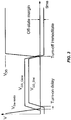
- FIG. 3 illustrates a timing diagram for a bootstrap circuit including an FET bootstrap device 102.
- the correct timing helps handle or eliminate the effects of severe conditions listed above. In operation, it takes time for the switch-node voltage to transition from high to low following the rise of the low side transistor 14 gate voltage. If the small synchronous FET bootstrap device 102 is turned on prematurely, the drain voltage will still be high. Under this condition the switch-node will be connected to the 5 V with disastrous consequences. Therefore, the turn on of the synchronous FET bootstrap device 102 must be adequately delayed to prevent this from happening. This delay is illustrated in Fig. 3 as the difference in the rise of V GS_Qlow and V GS_BTST . For similar reasons, the turn off of the synchronous FET bootstrap device 102 must occur at the same time as the low side transistor 14. This is also illustrated in FIG. 3 .
- both the low side transistor 14 and the synchronous FET bootstrap device 102 may be eGaN FET devices, both may have similar reverse conduction voltage drops when held off. Under these conditions it is possible for the synchronous FET bootstrap device 102 to reverse conduct main current either together with or instead of the low side transistor 14. This can lead to an over-voltage condition across the bootstrap capacitor 42 which can lead to failure of the high side transistor gate 28. To prevent this from occurring, in some embodiments, the off state voltage of the synchronous FET bootstrap device 102 is held at -1 V, thereby increasing the reverse conduction voltage to be significantly higher that the low side transistor 14 and thus, preventing it from conducting.
- FIG. 3 One example of an appropriate off-state margin is illustrated in FIG. 3 .
- preferred embodiments use a circuit layout that prevents the drain circuit of the bootstrap device 102 from ringing to higher voltages.
- the drain circuit of the synchronous FET bootstrap device 102 can ring to higher voltages that can charge the bootstrap capacitor 42 leading to failure of the high side transistor gate 28.
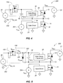
- FIG. 4 illustrates a bootstrap supply for a half bridge topology according to a comparative example 200 which is not part of the present invention.
- the comparative example of FIG. 4 includes many of the same components as the conventional half bridge topology 10 discussed above. Namely, high side and low side transistors 12 and 14 (Q1 and Q2), with their respective gates 28 and 32 coupled to a gate driver and level shifter 30 and a gate driver 34, respectively.
- the bootstrap device 102 (Q BTST ) is an unclamped enhancement mode device that is coupled between voltage source 36 (V Drvr ) and the bootstrap capacitor 42 (C BTST ).
- an additional supply voltage 202 V SD_GaN is also provided to the bootstrap device 102 (Q BTST ) to increase and overcome the voltage drop across the GaN FET body diode of the boot strap device 102 (Q BTST ).
- Voltage source 203 (V Drvr ) is applied to the low side gate driver 38 without the additional supply voltage 202 (V SD_GaN ).
- the configuration yields approximately 7.5 V across the bootstrap capacitor 42 (C BTST ) if the body diode of transistor 14 (Q 2 ) conducts.
- the gate driver 34 requires some form of regulation for this configuration. Depending on the comparative example, the gate driver 34 may be internally or externally regulated.
- the timing of the circuit 10 may regulate the low side gate driver 34.
- the voltage source 36 driving the circuit 10 may be regulated and that regulation may in turn be passed on to the bootstrap capacitor 42 when the circuit is operating correctly.
- the voltage across the source and drain V SD for the bootstrap device 102 (Q BTST ) should be the same or similar as the voltage across the source and drain for transistor 14 (Q2).
- the comparative example 300 in FIG. 5 illustrates a modification of the comparative example 200 of FIG. 4 .
- the primary difference is that the bootstrap supply is clamped with a Zener clamp 302 (i.e. , a Zener diode D CLMP ) that is coupled in parallel to the bootstrap capacitor 42 (C BTST ).
- a resistor 304 R llim is connected in series between the drain 108 of the bootstrap device 102 (Q BTST ) and the Zener clamp D CLMP .
- the Zener clamp 302 uses the Zener clamp 302 to keep the voltage across the bootstrap capacitor 42 (C BTST ) within safe operating limits if the body diode of transistor 14 (Q 2 ) conducts. Moreover, the Zener clamp 302 (D CLMP ) clamps the voltage to a safe limit for the transistor 12 (Q 1 ), and the resistor 304 (R llim ) provides voltage buffer during clamping. Similar to the embodiment 100 of FIG. 2 , the voltage across the source and drain V SD for the bootstrap device 102 (Q BTST ) should be the same or similar as the voltage across the source and drain for the transistor 14 (Q2). Similar to the configuration 200 of FIG.
- an additional supply voltage 202 (V SD_GaN ) is also provided to the bootstrap device 102 (Q BTST ) to overcome the voltage drop across the bootstrap device 102 body diode.
- the bootstrap device 102 is preferably a GaN FET.
- the resistor 304 that provides the current limiting function can be integrated into the bootstrap device 102 (Q BTST ).
- the resistor can be integrated by using RDS(on), i.e., with the internal resistance of the FET providing the appropriate resistance.
- a resistive element may be added, such as a metal busing for example.
- other resistive elements may be used.
- One advantage to integrating resistive element 304 is that it would eliminate an external component.
- the Zener clamp 302 may be achieved by using two enhancement GaN FETs connected in series with the gates of each shorted to their respective sources. This design would enable maximum integration for the circuit design.
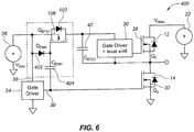
- FIG. 6 illustrates a bootstrap supply for a half bridge topology according to an additional comparative example 400 of the present disclosure.
- the design of FIG. 6 includes many of the same components as the half bridge topology discussed above with respect to embodiment 100 shown in FIG. 2 .
- comparative example 400 includes high side and low side transistors 12 and 14 (Q1 and Q2), with their respective gates 28 and 32 coupled to a gate driver and level shifter 30 and a gate driver 34, respectively.
- the bootstrap supply can be considered a synchronous enhancement mode device implementation.
- the bootstrap device 102 Q BTST is coupled between the driving voltage source 36 (V Drvr ) and the high side gate driver and level shifter 30.
- an enhancement diode 402 (D ENH ) is coupled between the driving voltage source 36 (V Drvr ) and the gate 106 of the bootstrap device 102 (Q BTST ).
- an enhancement capacitor 404 (C ENH ) is coupled between the gate 106 of the bootstrap device 102 (Q BTST ) and an output 38 of the low gate driver 34.
- the enhancement diode 402 (D ENH ) may be integrated into the bootstrap device 102 to reduce the number of external components.
- an enhancement mode resistor in parallel with the enhancement diode 402, may also be integrated into the bootstrap device 102.
- the bootstrap device 102 (Q BTST ) of the comparative example of FIG. 5 is synchronized to the switching of transistor 14 (Q2), which overcomes the 7.5 V across bootstrap capacitor 42 (C BTST ) discussed above for the conventional design. Synchronization prevents the "body diode" of the low side transistor 14 from over charging the high side transistor gate 28.
- the voltage across the source and drain V SD for the bootstrap device 102 (Q BTST ) should be the same as the voltage across the source and drain for the transistor 14 (Q2).
- the voltage between the gate and the source (V GS ) for transistor 14 (Q2) 0 volts and the voltage between the gate and the source (V GS ) for the bootstrap device 102 (Q BTST ) is -5 volts where the values of the drain current I D are worst case.
- the voltage drop of enhancement diode 402 (D ENH ) lowers the voltage across the gate and source V GS of the bootstrap device 102 (Q BTST ) to below 0 V and, therefore, raises the voltage across the source to drain V SD increasing the difference between transistor 14 (Q2) and the bootstrap device 102 (Q BTST ) for additional margin.
- the enhancement capacitor 404 (C ENH ) is charged (for example, to 5 V) in the same manner as a traditional boot-strap supply, but the enhancement diode 402 (D ENH ) used can be a low voltage (e.g., ⁇ 20 V) Schottky diode with zero or ultra-low reverse recovery charge Q RR .
- the voltage across the enhancement capacitor (C ENH ) can be controlled (reduced) to add additional body diode voltage margin of the bootstrap device 102 (Q BTST ) during the off state that further reduces the likelihood that the reverse voltage of the conduction of the body diode of transistor (Q2) can increase the bootstrap supply voltage above safe operating limits.
- Some embodiments may further include timing circuitry to allow the low side transistor 14 time to turn fully on before the bootstrap transistor 102 turns on.
- the timing circuit may also immediately, or as quickly as possible, turn off the bootstrap transistor 102 when the voltage at the gate of the low side transistor 14 is reduced to zero (0).
- the embodiment and comparative examples described above can be sensitive to drain inductance of the bootstrap transistor 102, which can ring if not kept in check.
- a small series resistor may be added in series after the drain of the bootstrap transistor 102.
- This resistor may be integrated to the bootstrap transistor 102.
- the resistor may be integrated by designing the bootstrap transistor 102 with a high RDS(on) approximately 3 ⁇ .
- the resistor may just be an integrated damping resistor (not RDS(on) but discrete).
- the transistor used for the bootstrap device of the examply embodiment of Fig. 2 is a depletion mode GaN FET, and the transistors used for the bootstrap device of each comparative examples shown in FIGs. 4-6 are preferably GaN FETs.
- the configurations for boot-strap device discussed above are provided to drive gallium nitride "GaN" FETs, but the comparative examples are in no way limited and can also be used to drive regular MOSFETs ( e.g ., for a half bridge topology).
- the techniques discussed above will not work using a MOSFET as the bootstrap device 102 if the half bridge transistor are also MOSFETs.
- the bootstrap transistor MUST make use of the reverse conduction voltage characteristic of GaN where the voltage drop can be programmed by the magnitude of the negative gate voltage. This buys the immunity from the internal diode from conducting when it should not. MOSFETs can not perform in this manner and thus, could become part of the main power circuit with disastrous consequences. 2) MOSFETs have Qrr whereas eGaN FETs do not. Should the MOSFET diode conduct (for whatever reason), the benefits of the techniques taught here, will be completely lost.
Landscapes
- Engineering & Computer Science (AREA)
- Computer Hardware Design (AREA)
- Physics & Mathematics (AREA)
- Computing Systems (AREA)
- General Engineering & Computer Science (AREA)
- Mathematical Physics (AREA)
- Electronic Switches (AREA)
- Power Conversion In General (AREA)
- Dc-Dc Converters (AREA)
Applications Claiming Priority (2)
| Application Number | Priority Date | Filing Date | Title |
|---|---|---|---|
| US201462062445P | 2014-10-10 | 2014-10-10 | |
| PCT/US2015/054851 WO2016057878A1 (en) | 2014-10-10 | 2015-10-09 | High voltage zero qrr bootstrap supply |
Publications (3)
| Publication Number | Publication Date |
|---|---|
| EP3205021A1 EP3205021A1 (en) | 2017-08-16 |
| EP3205021A4 EP3205021A4 (en) | 2018-06-13 |
| EP3205021B1 true EP3205021B1 (en) | 2021-12-01 |
Family
ID=55653829
Family Applications (1)
| Application Number | Title | Priority Date | Filing Date |
|---|---|---|---|
| EP15848411.3A Active EP3205021B1 (en) | 2014-10-10 | 2015-10-09 | High voltage zero qrr bootstrap supply |
Country Status (7)
Cited By (1)
| Publication number | Priority date | Publication date | Assignee | Title |
|---|---|---|---|---|
| WO2023107885A1 (en) * | 2021-12-08 | 2023-06-15 | Efficient Power Conversion Corporation | Active bootstrapping drivers |
Families Citing this family (34)
| Publication number | Priority date | Publication date | Assignee | Title |
|---|---|---|---|---|
| TWI566328B (zh) * | 2013-07-29 | 2017-01-11 | 高效電源轉換公司 | 具有用於產生附加構件之多晶矽層的氮化鎵電晶體 |
| JP6378003B2 (ja) * | 2014-08-27 | 2018-08-22 | ラピスセミコンダクタ株式会社 | 半導体装置、電池監視システム、及び半導体装置の起動方法 |
| TWI641218B (zh) | 2016-05-25 | 2018-11-11 | 高效電源轉換公司 | 增強模式fet閘極驅動器ic |
| US10394260B2 (en) * | 2016-06-30 | 2019-08-27 | Synaptics Incorporated | Gate boosting circuit and method for an integrated power stage |
| JP6828296B2 (ja) * | 2016-08-09 | 2021-02-10 | 株式会社Gsユアサ | 蓄電装置および蓄電装置の充電制御方法 |
| CN110024290B (zh) * | 2016-12-01 | 2021-04-13 | 宜普电源转换公司 | 用于基于GaN晶体管的功率转换器的自举电容器过电压管理电路 |
| US10103629B2 (en) * | 2017-02-14 | 2018-10-16 | Nxp B.V. | High side driver without dedicated supply in high voltage applications |
| WO2018191154A1 (en) * | 2017-04-10 | 2018-10-18 | Microchip Technology Incorporated | Slew control for high-side switch |
| US10637456B2 (en) | 2017-07-20 | 2020-04-28 | Efficient Power Conversion Corporation | Low voltage drop cascaded synchronous bootstrap supply circuit |
| US10193554B1 (en) * | 2017-11-15 | 2019-01-29 | Navitas Semiconductor, Inc. | Capacitively coupled level shifter |
| US10778219B2 (en) | 2017-11-15 | 2020-09-15 | Navitas Semiconductor, Inc. | Level shifting in a GaN half bridge circuit |
| TWI663821B (zh) * | 2018-01-11 | 2019-06-21 | 晶豪科技股份有限公司 | 自舉式電路以及使用該自舉式電路之關聯的直流轉直流轉換器 |
| US11070203B2 (en) * | 2018-02-19 | 2021-07-20 | Cirrus Logic, Inc. | Dual bootstrapping for an open-loop pulse width modulation driver |
| CN108494234B (zh) * | 2018-04-09 | 2020-05-01 | 电子科技大学 | 适用于GaN高速栅驱动电路的浮动电源轨 |
| US10742121B2 (en) * | 2018-06-29 | 2020-08-11 | Dialog Semiconductor Inc. | Boot strap capacitor charging for switching power converters |
| CN112425057A (zh) | 2018-07-19 | 2021-02-26 | 三菱电机株式会社 | 电力变换装置、马达驱动装置以及空气调节器 |
| US10536070B1 (en) * | 2018-08-01 | 2020-01-14 | Infineon Technologies Ag | Driver for switching gallium nitride (GaN) devices |
| TWI732280B (zh) * | 2018-08-28 | 2021-07-01 | 美商高效電源轉換公司 | 串級自舉式GaN功率開關及驅動器 |
| US11303116B2 (en) * | 2018-08-29 | 2022-04-12 | Allegro Microsystems, Llc | Methods and apparatus for electrical overstress protection |
| US10574229B1 (en) | 2019-01-23 | 2020-02-25 | Tagore Technology, Inc. | System and device for high-side supply |
| US10601302B1 (en) * | 2019-04-04 | 2020-03-24 | Navitas Semiconductor, Inc. | Bootstrap power supply circuit |
| CN109995235B (zh) * | 2019-04-30 | 2024-03-08 | 广东美的制冷设备有限公司 | 智能功率模块和电器设备 |
| WO2021145020A1 (ja) | 2020-01-14 | 2021-07-22 | ローム株式会社 | 半導体装置 |
| KR102230129B1 (ko) * | 2020-01-31 | 2021-03-22 | 청주대학교 산학협력단 | 부트스트랩 회로 및 이를 포함하는 전원 공급 장치 |
| JP7232208B2 (ja) | 2020-03-19 | 2023-03-02 | 株式会社東芝 | 半導体装置 |
| IT202000016072A1 (it) | 2020-07-02 | 2022-01-02 | St Microelectronics Srl | Circuito di pilotaggio, dispositivo e procedimento di funzionamento corrispondenti |
| CN216672983U (zh) | 2020-07-02 | 2022-06-03 | 意法半导体股份有限公司 | 电路及电子设备 |
| CN113054831B (zh) * | 2021-04-30 | 2022-03-29 | 杰华特微电子股份有限公司 | 一种三电平开关电路 |
| CN113746305B (zh) * | 2021-08-30 | 2023-04-25 | 深圳数马电子技术有限公司 | 栅极驱动电路和多相智能功率模块 |
| TWI778854B (zh) * | 2021-11-03 | 2022-09-21 | 新唐科技股份有限公司 | 電子系統及晶片 |
| CN114421946B (zh) * | 2022-01-19 | 2024-07-02 | 科能芯(深圳)半导体有限公司 | 一种低反向导通压降的耗尽型功率器件的直驱电路 |
| TWI871686B (zh) | 2022-06-29 | 2025-02-01 | 美商高效電源轉換公司 | 通用功率場效電晶體(fet)驅動器積體電路(ic)架構 |
| US12381478B2 (en) * | 2023-05-23 | 2025-08-05 | Murata Manufacturing Co., Ltd. | Circuits and methods to startup and shutdown multi-level converters |
| CN117767711B (zh) * | 2024-02-22 | 2024-05-24 | 杰华特微电子股份有限公司 | 单向导通电路、桥式驱动电路及开关电源 |
Citations (1)
| Publication number | Priority date | Publication date | Assignee | Title |
|---|---|---|---|---|
| US20110018613A1 (en) * | 2009-07-21 | 2011-01-27 | Intersil Americas Inc. | System and method for pre-charging a boot capacitor in a switching regulator with high pre-bias voltage |
Family Cites Families (19)
| Publication number | Priority date | Publication date | Assignee | Title |
|---|---|---|---|---|
| US5182468A (en) * | 1989-02-13 | 1993-01-26 | Ibm Corporation | Current limiting clamp circuit |
| US5373435A (en) | 1993-05-07 | 1994-12-13 | Philips Electronics North America Corporation | High voltage integrated circuit driver for half-bridge circuit employing a bootstrap diode emulator |
| JP3219019B2 (ja) * | 1997-05-30 | 2001-10-15 | 関西日本電気株式会社 | 異常電流検出回路およびそれを用いた負荷駆動回路 |
| US7456658B2 (en) | 2006-04-07 | 2008-11-25 | International Rectifier Corporation | Circuit to optimize charging of bootstrap capacitor with bootstrap diode emulator |
| JP2007318891A (ja) * | 2006-05-25 | 2007-12-06 | Toyota Industries Corp | スイッチング素子駆動用電源回路 |
| TW200835125A (en) | 2007-02-08 | 2008-08-16 | Richtek Techohnology Corp | Circuit for charging the boot-strap capacitor of voltage converter |
| US20080290841A1 (en) | 2007-05-23 | 2008-11-27 | Richtek Technology Corporation | Charging Circuit for Bootstrap Capacitor and Integrated Driver Circuit Using Same |
| US7839131B2 (en) * | 2007-06-27 | 2010-11-23 | International Rectifier Corporation | Gate driving scheme for depletion mode devices in buck converters |
| US8659275B2 (en) | 2008-01-11 | 2014-02-25 | International Rectifier Corporation | Highly efficient III-nitride power conversion circuit |
| US8063616B2 (en) | 2008-01-11 | 2011-11-22 | International Rectifier Corporation | Integrated III-nitride power converter circuit |
| JP5457826B2 (ja) * | 2009-12-28 | 2014-04-02 | 株式会社ジャパンディスプレイ | レベルシフト回路、信号駆動回路、表示装置および電子機器 |
| JP4968487B2 (ja) * | 2010-03-08 | 2012-07-04 | サンケン電気株式会社 | ゲートドライブ回路 |
| CN103004071B (zh) | 2010-07-30 | 2016-05-25 | 奥的斯电梯公司 | 调节的自举电力供应 |
| JP2013062717A (ja) * | 2011-09-14 | 2013-04-04 | Mitsubishi Electric Corp | 半導体装置 |
| JP5236822B1 (ja) | 2012-01-30 | 2013-07-17 | シャープ株式会社 | ドライバ回路 |
| US9209793B2 (en) * | 2012-02-17 | 2015-12-08 | Infineon Technologies Austria Ag | Bootstrap circuitry for an IGBT |
| US8593211B2 (en) * | 2012-03-16 | 2013-11-26 | Texas Instruments Incorporated | System and apparatus for driver circuit for protection of gates of GaN FETs |
| CN103683872A (zh) * | 2012-09-11 | 2014-03-26 | 深圳市海洋王照明工程有限公司 | 一种半桥驱动电路 |
| US9171738B2 (en) * | 2012-12-18 | 2015-10-27 | Infineon Technologies Austria Ag | Systems and methods for integrating bootstrap circuit elements in power transistors and other devices |
-
2015
- 2015-10-07 US US14/877,613 patent/US9667245B2/en active Active
- 2015-10-08 TW TW104133258A patent/TWI607626B/zh active
- 2015-10-09 EP EP15848411.3A patent/EP3205021B1/en active Active
- 2015-10-09 CN CN201580056930.1A patent/CN107078736B/zh active Active
- 2015-10-09 JP JP2017519239A patent/JP6703983B2/ja active Active
- 2015-10-09 WO PCT/US2015/054851 patent/WO2016057878A1/en active Application Filing
- 2015-10-09 KR KR1020177012061A patent/KR102458233B1/ko active Active
-
2017
- 2017-04-26 US US15/497,637 patent/US10084445B2/en active Active
Patent Citations (1)
| Publication number | Priority date | Publication date | Assignee | Title |
|---|---|---|---|---|
| US20110018613A1 (en) * | 2009-07-21 | 2011-01-27 | Intersil Americas Inc. | System and method for pre-charging a boot capacitor in a switching regulator with high pre-bias voltage |
Cited By (3)
| Publication number | Priority date | Publication date | Assignee | Title |
|---|---|---|---|---|
| WO2023107885A1 (en) * | 2021-12-08 | 2023-06-15 | Efficient Power Conversion Corporation | Active bootstrapping drivers |
| TWI854388B (zh) * | 2021-12-08 | 2024-09-01 | 美商高效電源轉換公司 | 主動自舉式驅動器 |
| US12113524B2 (en) | 2021-12-08 | 2024-10-08 | Efficient Power Conversion Corporation | Active bootstrapping drivers |
Also Published As
| Publication number | Publication date |
|---|---|
| CN107078736A (zh) | 2017-08-18 |
| EP3205021A1 (en) | 2017-08-16 |
| JP6703983B2 (ja) | 2020-06-03 |
| US20160105173A1 (en) | 2016-04-14 |
| TWI607626B (zh) | 2017-12-01 |
| TW201622348A (zh) | 2016-06-16 |
| EP3205021A4 (en) | 2018-06-13 |
| KR20170069244A (ko) | 2017-06-20 |
| JP2017537584A (ja) | 2017-12-14 |
| US9667245B2 (en) | 2017-05-30 |
| CN107078736B (zh) | 2021-01-22 |
| US20170230046A1 (en) | 2017-08-10 |
| WO2016057878A1 (en) | 2016-04-14 |
| US10084445B2 (en) | 2018-09-25 |
| KR102458233B1 (ko) | 2022-10-24 |
Similar Documents
| Publication | Publication Date | Title |
|---|---|---|
| EP3205021B1 (en) | High voltage zero qrr bootstrap supply | |
| US9954522B2 (en) | Hybrid switch including GaN HEMT and MOSFET | |
| EP3590189B1 (en) | Hybrid switch control | |
| US8816666B2 (en) | Semiconductor switching device drive circuit using a limited drive voltage | |
| CN105939151B (zh) | 电子电路 | |
| JP5934925B2 (ja) | ゲートドライバおよびこれを備えたパワーモジュール | |
| US9397563B2 (en) | Driver circuit | |
| WO2021117821A1 (ja) | スイッチング回路のゲート駆動回路およびスイッチング電源の制御回路 | |
| TW201607244A (zh) | 包含高功率增強模式的氮化鎵電晶體與驅動電路的電源切換系統 | |
| JP2019519150A (ja) | エンハンスメントモードfetドライバic | |
| US10469065B2 (en) | Multi-level gate control for transistor devices | |
| US20170264210A1 (en) | Chattering-less rectification circuit | |
| JP6271723B2 (ja) | ドライバ回路 | |
| JP6572123B2 (ja) | ゲート駆動回路 | |
| EP3070830B1 (en) | Rectifier circuit with reduced reverse recovery time | |
| HK1242058A1 (en) | High voltage zero qrr bootstrap supply | |
| HK1242058B (zh) | 高電壓零反向恢復電荷自舉供應器 | |
| JP2013030893A (ja) | 低Vf逆導通FET回路及び多機能FET回路用IC |
Legal Events
| Date | Code | Title | Description |
|---|---|---|---|
| STAA | Information on the status of an ep patent application or granted ep patent |
Free format text: STATUS: THE INTERNATIONAL PUBLICATION HAS BEEN MADE |
|
| PUAI | Public reference made under article 153(3) epc to a published international application that has entered the european phase |
Free format text: ORIGINAL CODE: 0009012 |
|
| STAA | Information on the status of an ep patent application or granted ep patent |
Free format text: STATUS: REQUEST FOR EXAMINATION WAS MADE |
|
| 17P | Request for examination filed |
Effective date: 20170509 |
|
| AK | Designated contracting states |
Kind code of ref document: A1 Designated state(s): AL AT BE BG CH CY CZ DE DK EE ES FI FR GB GR HR HU IE IS IT LI LT LU LV MC MK MT NL NO PL PT RO RS SE SI SK SM TR |
|
| AX | Request for extension of the european patent |
Extension state: BA ME |
|
| RIN1 | Information on inventor provided before grant (corrected) |
Inventor name: DE ROOIJ, MICHAEL A. Inventor name: REUSCH, DAVID C. Inventor name: STRYDOM, JOHAN T. |
|
| DAV | Request for validation of the european patent (deleted) | ||
| DAX | Request for extension of the european patent (deleted) | ||
| A4 | Supplementary search report drawn up and despatched |
Effective date: 20180511 |
|
| RIC1 | Information provided on ipc code assigned before grant |
Ipc: H03K 17/687 20060101AFI20180504BHEP |
|
| STAA | Information on the status of an ep patent application or granted ep patent |
Free format text: STATUS: EXAMINATION IS IN PROGRESS |
|
| 17Q | First examination report despatched |
Effective date: 20200422 |
|
| REG | Reference to a national code |
Ref country code: DE Ref legal event code: R079 Ref document number: 602015075510 Country of ref document: DE Free format text: PREVIOUS MAIN CLASS: H03K0017687000 Ipc: H03K0017960000 |
|
| GRAP | Despatch of communication of intention to grant a patent |
Free format text: ORIGINAL CODE: EPIDOSNIGR1 |
|
| STAA | Information on the status of an ep patent application or granted ep patent |
Free format text: STATUS: GRANT OF PATENT IS INTENDED |
|
| RIC1 | Information provided on ipc code assigned before grant |
Ipc: H03K 17/96 20060101AFI20210525BHEP |
|
| INTG | Intention to grant announced |
Effective date: 20210615 |
|
| GRAS | Grant fee paid |
Free format text: ORIGINAL CODE: EPIDOSNIGR3 |
|
| GRAA | (expected) grant |
Free format text: ORIGINAL CODE: 0009210 |
|
| STAA | Information on the status of an ep patent application or granted ep patent |
Free format text: STATUS: THE PATENT HAS BEEN GRANTED |
|
| AK | Designated contracting states |
Kind code of ref document: B1 Designated state(s): AL AT BE BG CH CY CZ DE DK EE ES FI FR GB GR HR HU IE IS IT LI LT LU LV MC MK MT NL NO PL PT RO RS SE SI SK SM TR |
|
| REG | Reference to a national code |
Ref country code: GB Ref legal event code: FG4D |
|
| REG | Reference to a national code |
Ref country code: AT Ref legal event code: REF Ref document number: 1452752 Country of ref document: AT Kind code of ref document: T Effective date: 20211215 Ref country code: CH Ref legal event code: EP |
|
| REG | Reference to a national code |
Ref country code: IE Ref legal event code: FG4D |
|
| REG | Reference to a national code |
Ref country code: DE Ref legal event code: R096 Ref document number: 602015075510 Country of ref document: DE |
|
| REG | Reference to a national code |
Ref country code: LT Ref legal event code: MG9D |
|
| REG | Reference to a national code |
Ref country code: NL Ref legal event code: MP Effective date: 20211201 |
|
| REG | Reference to a national code |
Ref country code: AT Ref legal event code: MK05 Ref document number: 1452752 Country of ref document: AT Kind code of ref document: T Effective date: 20211201 |
|
| PG25 | Lapsed in a contracting state [announced via postgrant information from national office to epo] |
Ref country code: RS Free format text: LAPSE BECAUSE OF FAILURE TO SUBMIT A TRANSLATION OF THE DESCRIPTION OR TO PAY THE FEE WITHIN THE PRESCRIBED TIME-LIMIT Effective date: 20211201 Ref country code: LT Free format text: LAPSE BECAUSE OF FAILURE TO SUBMIT A TRANSLATION OF THE DESCRIPTION OR TO PAY THE FEE WITHIN THE PRESCRIBED TIME-LIMIT Effective date: 20211201 Ref country code: FI Free format text: LAPSE BECAUSE OF FAILURE TO SUBMIT A TRANSLATION OF THE DESCRIPTION OR TO PAY THE FEE WITHIN THE PRESCRIBED TIME-LIMIT Effective date: 20211201 Ref country code: BG Free format text: LAPSE BECAUSE OF FAILURE TO SUBMIT A TRANSLATION OF THE DESCRIPTION OR TO PAY THE FEE WITHIN THE PRESCRIBED TIME-LIMIT Effective date: 20220301 Ref country code: AT Free format text: LAPSE BECAUSE OF FAILURE TO SUBMIT A TRANSLATION OF THE DESCRIPTION OR TO PAY THE FEE WITHIN THE PRESCRIBED TIME-LIMIT Effective date: 20211201 |
|
| PG25 | Lapsed in a contracting state [announced via postgrant information from national office to epo] |
Ref country code: SE Free format text: LAPSE BECAUSE OF FAILURE TO SUBMIT A TRANSLATION OF THE DESCRIPTION OR TO PAY THE FEE WITHIN THE PRESCRIBED TIME-LIMIT Effective date: 20211201 Ref country code: PL Free format text: LAPSE BECAUSE OF FAILURE TO SUBMIT A TRANSLATION OF THE DESCRIPTION OR TO PAY THE FEE WITHIN THE PRESCRIBED TIME-LIMIT Effective date: 20211201 Ref country code: NO Free format text: LAPSE BECAUSE OF FAILURE TO SUBMIT A TRANSLATION OF THE DESCRIPTION OR TO PAY THE FEE WITHIN THE PRESCRIBED TIME-LIMIT Effective date: 20220301 Ref country code: LV Free format text: LAPSE BECAUSE OF FAILURE TO SUBMIT A TRANSLATION OF THE DESCRIPTION OR TO PAY THE FEE WITHIN THE PRESCRIBED TIME-LIMIT Effective date: 20211201 Ref country code: HR Free format text: LAPSE BECAUSE OF FAILURE TO SUBMIT A TRANSLATION OF THE DESCRIPTION OR TO PAY THE FEE WITHIN THE PRESCRIBED TIME-LIMIT Effective date: 20211201 Ref country code: GR Free format text: LAPSE BECAUSE OF FAILURE TO SUBMIT A TRANSLATION OF THE DESCRIPTION OR TO PAY THE FEE WITHIN THE PRESCRIBED TIME-LIMIT Effective date: 20220302 Ref country code: ES Free format text: LAPSE BECAUSE OF FAILURE TO SUBMIT A TRANSLATION OF THE DESCRIPTION OR TO PAY THE FEE WITHIN THE PRESCRIBED TIME-LIMIT Effective date: 20211201 |
|
| PG25 | Lapsed in a contracting state [announced via postgrant information from national office to epo] |
Ref country code: NL Free format text: LAPSE BECAUSE OF FAILURE TO SUBMIT A TRANSLATION OF THE DESCRIPTION OR TO PAY THE FEE WITHIN THE PRESCRIBED TIME-LIMIT Effective date: 20211201 |
|
| PG25 | Lapsed in a contracting state [announced via postgrant information from national office to epo] |
Ref country code: SM Free format text: LAPSE BECAUSE OF FAILURE TO SUBMIT A TRANSLATION OF THE DESCRIPTION OR TO PAY THE FEE WITHIN THE PRESCRIBED TIME-LIMIT Effective date: 20211201 Ref country code: SK Free format text: LAPSE BECAUSE OF FAILURE TO SUBMIT A TRANSLATION OF THE DESCRIPTION OR TO PAY THE FEE WITHIN THE PRESCRIBED TIME-LIMIT Effective date: 20211201 Ref country code: RO Free format text: LAPSE BECAUSE OF FAILURE TO SUBMIT A TRANSLATION OF THE DESCRIPTION OR TO PAY THE FEE WITHIN THE PRESCRIBED TIME-LIMIT Effective date: 20211201 Ref country code: PT Free format text: LAPSE BECAUSE OF FAILURE TO SUBMIT A TRANSLATION OF THE DESCRIPTION OR TO PAY THE FEE WITHIN THE PRESCRIBED TIME-LIMIT Effective date: 20220401 Ref country code: EE Free format text: LAPSE BECAUSE OF FAILURE TO SUBMIT A TRANSLATION OF THE DESCRIPTION OR TO PAY THE FEE WITHIN THE PRESCRIBED TIME-LIMIT Effective date: 20211201 Ref country code: CZ Free format text: LAPSE BECAUSE OF FAILURE TO SUBMIT A TRANSLATION OF THE DESCRIPTION OR TO PAY THE FEE WITHIN THE PRESCRIBED TIME-LIMIT Effective date: 20211201 |
|
| REG | Reference to a national code |
Ref country code: DE Ref legal event code: R097 Ref document number: 602015075510 Country of ref document: DE |
|
| PG25 | Lapsed in a contracting state [announced via postgrant information from national office to epo] |
Ref country code: IS Free format text: LAPSE BECAUSE OF FAILURE TO SUBMIT A TRANSLATION OF THE DESCRIPTION OR TO PAY THE FEE WITHIN THE PRESCRIBED TIME-LIMIT Effective date: 20220401 |
|
| PLBE | No opposition filed within time limit |
Free format text: ORIGINAL CODE: 0009261 |
|
| STAA | Information on the status of an ep patent application or granted ep patent |
Free format text: STATUS: NO OPPOSITION FILED WITHIN TIME LIMIT |
|
| PG25 | Lapsed in a contracting state [announced via postgrant information from national office to epo] |
Ref country code: DK Free format text: LAPSE BECAUSE OF FAILURE TO SUBMIT A TRANSLATION OF THE DESCRIPTION OR TO PAY THE FEE WITHIN THE PRESCRIBED TIME-LIMIT Effective date: 20211201 Ref country code: AL Free format text: LAPSE BECAUSE OF FAILURE TO SUBMIT A TRANSLATION OF THE DESCRIPTION OR TO PAY THE FEE WITHIN THE PRESCRIBED TIME-LIMIT Effective date: 20211201 |
|
| 26N | No opposition filed |
Effective date: 20220902 |
|
| PG25 | Lapsed in a contracting state [announced via postgrant information from national office to epo] |
Ref country code: SI Free format text: LAPSE BECAUSE OF FAILURE TO SUBMIT A TRANSLATION OF THE DESCRIPTION OR TO PAY THE FEE WITHIN THE PRESCRIBED TIME-LIMIT Effective date: 20211201 |
|
| PG25 | Lapsed in a contracting state [announced via postgrant information from national office to epo] |
Ref country code: MC Free format text: LAPSE BECAUSE OF FAILURE TO SUBMIT A TRANSLATION OF THE DESCRIPTION OR TO PAY THE FEE WITHIN THE PRESCRIBED TIME-LIMIT Effective date: 20211201 |
|
| REG | Reference to a national code |
Ref country code: CH Ref legal event code: PL |
|
| REG | Reference to a national code |
Ref country code: BE Ref legal event code: MM Effective date: 20221031 |
|
| GBPC | Gb: european patent ceased through non-payment of renewal fee |
Effective date: 20221009 |
|
| PG25 | Lapsed in a contracting state [announced via postgrant information from national office to epo] |
Ref country code: LU Free format text: LAPSE BECAUSE OF NON-PAYMENT OF DUE FEES Effective date: 20221009 |
|
| PG25 | Lapsed in a contracting state [announced via postgrant information from national office to epo] |
Ref country code: LI Free format text: LAPSE BECAUSE OF NON-PAYMENT OF DUE FEES Effective date: 20221031 Ref country code: FR Free format text: LAPSE BECAUSE OF NON-PAYMENT OF DUE FEES Effective date: 20221031 Ref country code: CH Free format text: LAPSE BECAUSE OF NON-PAYMENT OF DUE FEES Effective date: 20221031 |
|
| PG25 | Lapsed in a contracting state [announced via postgrant information from national office to epo] |
Ref country code: BE Free format text: LAPSE BECAUSE OF NON-PAYMENT OF DUE FEES Effective date: 20221031 |
|
| PG25 | Lapsed in a contracting state [announced via postgrant information from national office to epo] |
Ref country code: IE Free format text: LAPSE BECAUSE OF NON-PAYMENT OF DUE FEES Effective date: 20221009 Ref country code: GB Free format text: LAPSE BECAUSE OF NON-PAYMENT OF DUE FEES Effective date: 20221009 |
|
| PG25 | Lapsed in a contracting state [announced via postgrant information from national office to epo] |
Ref country code: HU Free format text: LAPSE BECAUSE OF FAILURE TO SUBMIT A TRANSLATION OF THE DESCRIPTION OR TO PAY THE FEE WITHIN THE PRESCRIBED TIME-LIMIT; INVALID AB INITIO Effective date: 20151009 |
|
| PG25 | Lapsed in a contracting state [announced via postgrant information from national office to epo] |
Ref country code: CY Free format text: LAPSE BECAUSE OF FAILURE TO SUBMIT A TRANSLATION OF THE DESCRIPTION OR TO PAY THE FEE WITHIN THE PRESCRIBED TIME-LIMIT Effective date: 20211201 |
|
| PG25 | Lapsed in a contracting state [announced via postgrant information from national office to epo] |
Ref country code: MK Free format text: LAPSE BECAUSE OF FAILURE TO SUBMIT A TRANSLATION OF THE DESCRIPTION OR TO PAY THE FEE WITHIN THE PRESCRIBED TIME-LIMIT Effective date: 20211201 |
|
| PG25 | Lapsed in a contracting state [announced via postgrant information from national office to epo] |
Ref country code: TR Free format text: LAPSE BECAUSE OF FAILURE TO SUBMIT A TRANSLATION OF THE DESCRIPTION OR TO PAY THE FEE WITHIN THE PRESCRIBED TIME-LIMIT Effective date: 20211201 |
|
| PG25 | Lapsed in a contracting state [announced via postgrant information from national office to epo] |
Ref country code: MT Free format text: LAPSE BECAUSE OF FAILURE TO SUBMIT A TRANSLATION OF THE DESCRIPTION OR TO PAY THE FEE WITHIN THE PRESCRIBED TIME-LIMIT Effective date: 20211201 |
|
| PGFP | Annual fee paid to national office [announced via postgrant information from national office to epo] |
Ref country code: IT Payment date: 20240926 Year of fee payment: 10 |
|
| PGFP | Annual fee paid to national office [announced via postgrant information from national office to epo] |
Ref country code: DE Payment date: 20240925 Year of fee payment: 10 |