EP3204987B1 - Vorrichtung, system und verfahren zur abschwächung von nebenkeulen mit einer gruppenantenne - Google Patents
Vorrichtung, system und verfahren zur abschwächung von nebenkeulen mit einer gruppenantenne Download PDFInfo
- Publication number
- EP3204987B1 EP3204987B1 EP15849491.4A EP15849491A EP3204987B1 EP 3204987 B1 EP3204987 B1 EP 3204987B1 EP 15849491 A EP15849491 A EP 15849491A EP 3204987 B1 EP3204987 B1 EP 3204987B1
- Authority
- EP
- European Patent Office
- Prior art keywords
- antenna
- signal
- emitters
- antennae
- emitter
- Prior art date
- Legal status (The legal status is an assumption and is not a legal conclusion. Google has not performed a legal analysis and makes no representation as to the accuracy of the status listed.)
- Active
Links
Images


Classifications
-
- H—ELECTRICITY
- H01—ELECTRIC ELEMENTS
- H01Q—ANTENNAS, i.e. RADIO AERIALS
- H01Q3/00—Arrangements for changing or varying the orientation or the shape of the directional pattern of the waves radiated from an antenna or antenna system
- H01Q3/26—Arrangements for changing or varying the orientation or the shape of the directional pattern of the waves radiated from an antenna or antenna system varying the relative phase or relative amplitude of energisation between two or more active radiating elements; varying the distribution of energy across a radiating aperture
- H01Q3/30—Arrangements for changing or varying the orientation or the shape of the directional pattern of the waves radiated from an antenna or antenna system varying the relative phase or relative amplitude of energisation between two or more active radiating elements; varying the distribution of energy across a radiating aperture varying the relative phase between the radiating elements of an array
-
- H—ELECTRICITY
- H01—ELECTRIC ELEMENTS
- H01Q—ANTENNAS, i.e. RADIO AERIALS
- H01Q13/00—Waveguide horns or mouths; Slot antennas; Leaky-waveguide antennas; Equivalent structures causing radiation along the transmission path of a guided wave
- H01Q13/10—Resonant slot antennas
-
- H—ELECTRICITY
- H01—ELECTRIC ELEMENTS
- H01Q—ANTENNAS, i.e. RADIO AERIALS
- H01Q21/00—Antenna arrays or systems
- H01Q21/0006—Particular feeding systems
-
- H—ELECTRICITY
- H01—ELECTRIC ELEMENTS
- H01Q—ANTENNAS, i.e. RADIO AERIALS
- H01Q21/00—Antenna arrays or systems
- H01Q21/0006—Particular feeding systems
- H01Q21/0037—Particular feeding systems linear waveguide fed arrays
- H01Q21/0043—Slotted waveguides
- H01Q21/005—Slotted waveguides arrays
-
- H—ELECTRICITY
- H01—ELECTRIC ELEMENTS
- H01Q—ANTENNAS, i.e. RADIO AERIALS
- H01Q21/00—Antenna arrays or systems
- H01Q21/06—Arrays of individually energised antenna units similarly polarised and spaced apart
- H01Q21/061—Two dimensional planar arrays
- H01Q21/068—Two dimensional planar arrays using parallel coplanar travelling wave or leaky wave aerial units
-
- H—ELECTRICITY
- H01—ELECTRIC ELEMENTS
- H01Q—ANTENNAS, i.e. RADIO AERIALS
- H01Q21/00—Antenna arrays or systems
- H01Q21/06—Arrays of individually energised antenna units similarly polarised and spaced apart
- H01Q21/20—Arrays of individually energised antenna units similarly polarised and spaced apart the units being spaced along or adjacent to a curvilinear path
-
- H—ELECTRICITY
- H01—ELECTRIC ELEMENTS
- H01Q—ANTENNAS, i.e. RADIO AERIALS
- H01Q3/00—Arrangements for changing or varying the orientation or the shape of the directional pattern of the waves radiated from an antenna or antenna system
- H01Q3/24—Arrangements for changing or varying the orientation or the shape of the directional pattern of the waves radiated from an antenna or antenna system varying the orientation by switching energy from one active radiating element to another, e.g. for beam switching
Definitions
- Embodiments discussed herein generally relate to signal transmission devices. More particularly, certain embodiments include, but are not limited to, an antenna array configured to provide a signal phase difference.
- Various directional antenna systems including flat panel antennae with limited apertures, exhibit a response outside a main beam, known as side lobes.
- side lobes can cause unintended reception of adjacent satellite signals.
- side lobes can cause unintended interference with other RF signals on adjacent satellites.
- the Federal Communications Commission (FCC) regulates the levels of these side lobes.
- a width of the main beam and the size of side lobes are indicative of antenna performance characteristics. More particularly, a relatively narrow main beam and small side lobes correspond to better directional transmission characteristics. In the case of radio communications, good directional transmission enables more selective communication with a target device and/or better distinguishing by the target device of one transmitter from another nearby transmitter.
- US 6 429 825 B1 describes a cavity slot antenna array for a communications system such as a wireless network.
- US 4 475 107 A describes a microstrip line antenna which comprises a dielectric substrate having a ground plate formed on one surface thereof and at least a pair of stripline conductors bent periodically on the other surface to be applied a travelling-wave.
- EP 0159 301 A1 describes an electrically controlled aerial array with a main lobe which may be controlled by varying the phases in the included aerial elements.
- US 3 560 975 A describes an aircraft antenna array, the array being designed to implement a spatial aerial navigation method based upon the continuous or periodic plotting of the aircraft's position in relation to two points fixed in space, which points may be located outside the earth's atmosphere.
- GB 881 748 A describes a radiant energy system for radiating and receiving electromagnetic energy including an antenna, a receiver and first control means for modulating the electromagnetic energy fed to the antenna.
- an antenna array, a system and a method at an antenna array are provided having the features of claims 1, 4 and 5.
- Preferable embodiments may include the additional features in accordance with one or more of the dependent claims.
- an antenna array includes a first antenna and a second antenna, where a first signal is provided at a first input of the first antenna while a second signal is provided at a second input of the second antenna.
- Signal emission from the first antenna and the second antenna is characterized by a phase differential other than a phase differential corresponding to the first input and the second input.
- the first antenna and the second antenna passively induce a change in a phase differential between the first signal and the second signal.
- side lobe characteristics is mitigated for electromagnetic (EM) emissions from the array.
- a phase difference between respective portions of the first signal and the second signal is emitted from the first antenna and second antenna respectively, wherein a passively-induced phase difference between these portions facilitates destructive interference of the first signal and the second signal with each other and/or with other signals that might be concurrently transmitted with the antenna array.
- Embodiments described herein variously provide for multiple antennae (channels) of an antenna array to each emit the same main beam energy, so that respective main beams of the channels sum across the array. However, some or all such channels may each emit a slightly different side lobe pattern. This difference between side lobe patterns is achieved at least in part by different respective physical characteristics of various antennae - e.g., where such different characteristics induce one or more signal phase changes.
- Differences in physical characteristics of antennae include lengths of propagation media having different dielectric properties.
- a delay of a signal - and a corresponding phase shift of that signal - is provided by a change in dielectric material along the length of an antenna.
- an antenna includes multiple sections of different propagation media to induce successive wave propagation rate changes along the length of the antenna.
- phase differentials between antennae of an array may avoid modes or other constructive interference patterns by the array.
- the array may provide a set of phase differences each between a respective pair of antennae.
- the set of phase differences may be chosen to avoid any two phase differences being integer multiples of one another.
- a distribution of phase differentials may be according to a distribution analogous to the "Circle of Fifths" for musical tones.
- the Circle of Fifths provides an audio frequency corollary to phase differentiation according to one embodiment, wherein a middle C note is at 256 Hz, and the G note above middle C is 1.5 times that frequency.
- Each successive tone in the Circle of Fifths (C, G, D, A, E, B, F#, C#, G#, D#, A#, F) is 1.5 times that of the preceding tone.
- values may be variously divided - e.g., by 2, one or more several times as necessary - to facilitate placement of a set of corresponding difference values each in a 0° to 360° (0 to 2n radian) range.
- antennas of the array are each provided with a respective signal that propagates along a length of that array.
- the antenna array may induce a difference between phase differentials each for a given pair of signals to be variously transmitted from the array.
- a difference in phase differentials may be additionally induced at circuitry that is coupled to the antenna array.
- transmitter circuitry may be coupled to such an antenna array, the circuitry to exchange different signals each with a respective antenna of the antenna array.
- the circuitry may selectively delay or otherwise offset a phase of one or more such signals to provide for a difference between phase differentials each for a given pair of signals.
- phase offset may be distinguishable from phase modulation schemes, for example, at least insofar as the phase offset may be a static, unchanging offset applied throughout a communication exchange.
- the phase differentials aid in mitigating side lobes of a signal to be transmitted by the array and/or mitigate the effects of side lobes in a signal that has been received by the array.
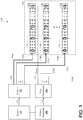
- FIG. 1 illustrates elements of a system 100 to transmit a signal with an antenna array according to an embodiment.
- System 100 may include any of a variety of radio, radar and/or other transmission devices.
- System 100 is one example of an embodiment wherein a signal is variously split into a plurality of component signals including a first signal and a second signal, where a first antenna of an antenna array is configured to be provided with the first signal concurrent with a second antenna of the antenna array being provided with the second signal.
- propagation of the first signal in the first antenna, and propagation of the second signal in the second antenna results in different phase differentials each between the first signal and the second signal.
- system 100 includes an antenna array 110 comprising a plurality of antennae - e.g., such as the illustrative antennae 112a, 112b,..., 112n.
- antennae - e.g., such as the illustrative antennae 112a, 112b,..., 112n.
- the particular number of antennae 112a, 112b,..., 112n, and their particular configuration with respect to one another, is merely illustrative, and not limiting on some embodiments.
- Antennae 112a, 112b,..., 112n may be configured each to transmit a respective one or more signals provided, for example, by a splitter 130.
- system 100 includes a source 120 - e.g., a radio signal source or a radar signal source - coupled to provide to splitter 130 a signal 122 that, for example, represents information to be communicated from system 100 via antenna array 110 to a remote device (not shown).
- splitter 130 may generate a set 132 of signals to be variously transmitted each with a different respective antenna of antenna array 110.
- generation of set 132 may include variously splitting power of signal 122, and outputting portions of such power each as a respective one of signals 134a, 134b,..., 134n.
- Antenna array 110 is an example of an antenna array configured to mitigate side lobes according to an embodiment.
- Antennae 112a, 112b,..., 112n each include a respective waveguide structure and a propagation media (not shown) disposed therein.
- respective inputs 116a, 116b,..., 116n of antennae 112a, 112b,..., 112n are each coupled to be provided from splitter 130 a respective one of signals 134a, 134b,..., 134n.
- signals 134a, 134b,..., 134n variously propagate away from inputs 116a, 116b,..., 116n each along the length of a respective one of antennae 112a, 112b,..., 112n.
- Antennae 112a, 112b,..., 112n may include emitters variously configured to emit portions of signals 134a, 134b,..., 134n for transmission.
- emitters 114a may be variously disposed along a length of antenna 112a, where different portions of signal 134a are to variously propagate to, and through, respective ones of emitters 114a.
- Emitters 114a may provide openings, apertures or other such structures to allow a signal pass-through at a sidewall in the waveguide of antenna 112a (where the signal propagates between sidewalls of the waveguide toward a far end of the waveguide).
- emitters 114b may be additionally or alternatively disposed along antenna 112b to variously emit portions of signal 134b, and/or emitters 114c disposed along antenna 112c may be variously configured to emit portions of signal 134c.
- system 100 may further comprise a pattern generator 140 including logic (e.g., circuitry and/or software) configured to determine a transmission pattern to be provide with antenna array 110.
- the pattern may be described by or otherwise communicated to drive electronics 150 based on pattern information 142 from pattern generator 140.
- drive electronics 150 may generate a set 152 of control signals to regulate signal emission from antenna array 110.
- set 152 may include control signals 154a, 154b,..., 154n to be received, respectively, at antennae 112a, 112b,..., 112n.
- antennae 112a, 112b,..., 112n may selectively open and/or close various respective ones of emitters 114a, 114b,..., 114n.
- Such selectively control of emitters 114a, 114b,..., 114n may enable shaping of a waveform - e.g., where such shaping is performed in concert with signal power allocation by splitting 130.
- phase differential refers to a difference, at a particular time, between the respective phases of two signals each propagating in a different respective antenna of an antenna array.
- a phase of a signal may depend on a location in the antenna - e.g., where, at a particular time under consideration, the signal in question has a first phase value at a particular location along a length of a given antenna.
- propagation of two signals in different respective antennae, in combination with different respective configurations of such antennae results in a difference between phase differentials for different locations of the antennae.
- signal 134a may have a phase ⁇ 11 at input 116a
- signal 134b may have a concurrent phase ⁇ 12 at input 116b.
- signal 134a may propagate away from input 116a and toward one of emitters 114a, where signal 134b concurrently propagates away from input 116b and toward one of emitters 114b.
- signal 134a may have a phase ⁇ 21 at a location other than input 116a - e.g., where signal 134b has a phase ⁇ 22 a location other than input 116b.
- either of ⁇ 2 and ⁇ 1 may be zero, a negative value or a positive value.
- ⁇ 21 corresponds to a particular one of emitters 114a and/or to a particular distance from input 116a. Additionally or alternatively, ⁇ 22 may correspond to a particular one of emitters 114b and/or to a particular distance from input 116b. For example, ⁇ 21 may correspond to an emitter that is the Nth closest one of emitters 114a to input 116a (where N is a positive integer), and ⁇ 22 may correspond to an emitter that is the Nth closest one of emitters 114b to input 116b. In such a scenario, a difference between ⁇ 2 and ⁇ 1 may be based at least in part on a difference between a configuration of antenna 112a and a configuration of antenna 112b.
- Such a difference between ⁇ 2 and ⁇ 1 may be independent, for example, of any changing phase of signal 134a over time and/or independent of any changing phase of signal 134b over time.
- the difference between ⁇ 2 and ⁇ 1 attributable to the different configurations of antennae 112a, 112b may be in addition to, but distinguishable from, any other change in phase difference that might be the result of phase modulation of signal 134a and/or signal 134b.
- a difference may result at least in part from emitters 114a having a distribution along antenna 112a that is different than a distribution of emitters 114b having along antenna 112b.
- a total number of emitters 114a may be different than a total number of emitters 114b.
- antennae 112a, 112b may have different respective overall lengths and/or a distance of input 116a from an Nth one of emitters 114a may be different than a distance of input 116b from an Nth one of emitters 114b.
- an arrangement of one or more propagation materials in antenna 112a is different than an arrangement of one or more propagation materials in antenna 112b.
- Antenna array 110 may include any of a variety of combinations of fewer, more and/or different antennae, according to different embodiments. Additionally or alternatively, certain embodiment may vary with respect to the number of emitters on any one antenna of array 110, and/or the positions of emitters on various antennae.
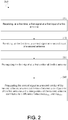
- FIG. 2 shows elements of a method 200 to operate an antenna array according to an embodiment.
- Method 200 may provide for operation of antenna array 110 and/or other components of system 100, for example.
- Antennae of the array may each include a respective waveguide structure and one or more propagation media disposed therein.
- Such antennae may each further comprise respective emitters variously formed in or on the waveguide structure. Although certain embodiments are not limited in this regard, some or all such emitters may be operable to selectively open or close in response to control signaling.
- method 200 includes, at 210, receiving, at a first time, a first signal at a first input of a first antenna.
- Method 200 may further comprise, at 220, receiving, at the first time, a second signal at a second input of a second antenna.
- the receiving at 210 may include input 116a receiving signal 134a, where the receiving at 220 includes input 116b receiving signal 134b.
- method 200 may include propagating the first signal at a first emitter of the first antenna.
- a portion of the signal may propagate through the first emitter, although certain embodiments are not limited in this regard.
- the first emitter may be an Nth closest emitter to the first input, wherein N is a positive integer.
- the first emitter may be the Nth emitter in a sequence of a first plurality of emitters from along a path extending from the first input along a length of the first antenna - e.g., where the first signal is to propagate along said path.
- Method 200 may further comprises, at 240, propagating the second signal at a second emitter of the second antenna - e.g., wherein, of all emitters of the second antenna, the second emitter is an Nth closest emitter to the second input.
- a difference between a configuration of the first antenna and a configuration of the second antenna contributes to a difference between a first phase differential, at the first time, between the first signal at the first input and the second signal at the second input and a second phase differential, at a second time, between the first signal at the first emitter and the second signal at the second emitter.
- the difference between the first phase differential and the second phase differential may be based at least in part on a first difference between a distance of the first emitter from the first input, and a distance of the second emitter from the second input.
- the first difference may be equal to or greater than a width of the first emitter (or alternatively, greater than a width of the second emitter).
- the first distance may be at least three (3) times - e.g., five (5) times or more than - the width of an emitter.
- the difference between the first phase differential and the second phase differential is based at least in part on different arrangements of respective propagation media of the first antenna and the second antenna having different configurations of respective propagation media.
- the first antenna may comprise a first medium disposed between the first input and the first emitter, where the second antenna comprises a second medium disposed between the second input and the second emitter.
- the first signal may propagate from the first input to the first emitter via the first medium
- the second signal may propagate from the second input to the second emitter via the second medium.
- the difference between the first phase differential and the second phase differential may be based at least in part on a difference between a permittivity of the first medium and a permittivity of the second medium.
- Such embodiments are merely some examples of how a difference between respective characteristics, intrinsic to antennae, may give rise to a change in phase differential as respective signals propagate through such antennae.
- Such changes in phase differential may be said to be passively induced, at least insofar as they are not the result of phase changes due to circuitry that is coupled to, and drives transmission by, the antenna array.
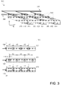
- FIG. 3 illustrates elements of an antenna array 300 to transmit signals according to an example useful for understanding the present invention.
- Antenna array 300 may include some or all features of antenna array 110, for example.
- operation of antenna array 300 is performed according to method 200.
- antenna array 300 includes a plurality of antennae each including a respective waveguide structure and a propagation medium disposed therein.
- array 300 may include antennae 310, 320, 330 comprising respective waveguide structures 312, 322, 332 and respective dielectric structures 314, 324, 334 variously disposed therein.
- waveguide structures 312, 322, 332 may each be straight and arranged in parallel with each other.
- Signals 350 may be variously provided to antennae 310, 320, 330 - e.g., from power splitter circuitry (not shown) coupled thereto.
- Antennae 310, 320, 330 may further comprise respective emitters 340 variously distributed each on a respective one of waveguide structures 312, 322, 332.
- Control signals 360 may be further coupled, in some examples, to selectively determine how signal power is to be variously output from different ones of emitters 340.
- Antenna array 300 is one example of an array, according to an example useful for understanding the present invention, including two antennae to concurrently be provided with different respective signals for transmission, where a difference between respective physical characteristics of the antennae results in a difference between phase differentials (each phase differential between the two signals).
- the top view 305 of antenna array 300 shows one example of various physical differences - between different pairs of antennae 310, 320, 330 - that variously facilitate differences in phase differentials for different pairs of signals 350.
- respective inputs 316, 326, 336 of 310, 320, 330 may be coupled each to receive a different respective one of signals 350.
- Two or more of antennae 310, 320, 330 may vary from one another at least with respect to a total numbers of emitters and/or a distribution of emitters.
- respective inputs 316, 326, 336 of antennae 310, 320, 330 may each be coupled to receive a respective one of signals 350.
- Inputs 316, 326, 336 may be aligned with each other, for example, along a line x0.
- an emitter of antenna 310 that is closest to input 316 may be offset from input 316 by a distance c1, where two other emitters of antenna 310 are variously offset by distances c2, c3.
- an emitter of antenna 320 that is closest to input 326 may be offset from input 326 by a distance b1 (e.g., different than c1), where three other emitters of antenna 320 are variously offset by distances b2, b3, b4.
- an emitter of antenna 330 that is closest to input 336 may be offset from input 336 by a distance a1 (which may be equal to, or different than, c1), where two other emitters of antenna 330 are variously offset by distances a2, a3.
- antenna array 300 may provide for a different phase differentials each between two signals - e.g., wherein a phase differential changes along the length of antennae as said signals variously propagate each in a respective one of antennae 310, 320, 330.
- an amount of a phase differential for signals at inputs 316, 326 e.g., the amount being zero
- antenna array 300 may provide for a different phase differentials each between two signals - e.g., wherein a phase differential changes along the length of antennae as said signals variously propagate each in a respective one of antennae 310, 320, 330.
- an amount of a phase differential for signals at inputs 316, 326 e.g., the amount being zero
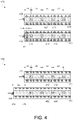
- FIG. 4 shows cross-sectional top views of antenna arrays 400, 450 each to transmit signals according to a corresponding embodiment and an example useful for understanding the present invention.
- One or each of antenna arrays 400, 450 may include features of antenna arrays 110, 300 - e.g. where operation of antenna array 400 or antenna array 450 is performed according to method 200.
- Antenna arrays 400, 450 illustrate an embodiment and an example useful for understanding the present invention that variously provide for change in signal phase differentials between two (or more) antennae, where the change is due in part to the propagation of signals, in respective antennae, through different dielectric structures.
- respective inputs 418, 428 of antennae 410, 420 are coupled each to receive a respective signal.
- Inputs 418, 428 may be aligned with one another along a line x1 that, for example, is perpendicular to a direction of alignment of antennae 410, 420.
- antennae 410, 420 may have the same number and arrangement of respective emitters. For example, offsets xa, xb, xc, xd from line x0 may variously define locations of the respective emitters of antennae 410, 420.
- a dielectric 424 disposed in a waveguide structure 422 of antenna 420, has a first permittivity and extends along the entire length of antenna 420.
- a dielectric 414 and a dielectric 416 disposed in a waveguide structure 412 of antenna 410, variously extend each only partially along the length of antenna 410, where each of dielectric 414 and dielectric 416 has a respective permittivity other than the first permittivity.
- an amount of a phase difference for signals at respective ones of inputs 418, 428 may be different - e.g., less than - a phase difference for the same signals at respective ones of the emitters at offset xa (for example).
- an antenna 460 includes a waveguide structure 462 and a dielectric material 464 disposed therein, wherein dielectric material 464 extends the entire length of antenna 460.
- an antenna 470 of array 450 may include a waveguide structure 472 and a dielectric material 474 disposed therein, wherein dielectric material 474 extends the entire length of antenna 470.
- a permittivity of dielectric material 464 may be equal to that of dielectric material 474.
- Inputs 468, 478 of antennae 460, 470 may be variously coupled each to receive a respective signal. Respective emitters of antennae 460, 470 may have the same total number and may have the same arrangement relative to one another - e.g., where offsets xa, xb, xc, xd variously define distances between pairs of such emitters. However, inputs 468, 478 may be offset by different respective distances each from a respective closest emitter. For example, inputs 468, 478 may be aligned with respective lines x2a, x2b that are offset from one another by a distance ⁇ x.
- offset xa separates input 478 from a closest emitter of antenna 470
- a greater distance ( ⁇ x + xa) separates input 468 from a closest emitter of antenna 460. Due to variation between the respective dielectric structures of antennae 460, 470, an amount of a phase difference for signals at respective ones of inputs 468, 478 may be different - e.g., less than - a phase difference for the same signals at the respective Nth emitters closest to inputs 468, 478.
- FIG. 5 illustrates elements of a method 500 for determining, according to an embodiment, a set of differences - each between a respective pair of phase differentials - to be provided with an antenna array.
- Design of an antenna array with method 500 may mitigate constructive interference between side lobes from different respective pairs of antennae in the array.
- Such an array may include one of arrays 110, 300, 400, 450, for example.
- Method 500 may comprise, at 505, setting respective values for variables and constants used to determine a set of difference values.
- values w and y represent, respectively, a total number of difference values ( ⁇ s) to be determined by method 500, and a phase difference variable.
- Values x 1 , x 2 , x 3 are constant values to be used in recursive processing with the value y.
- a counter value i may be set to an initial value (e.g., 1), where i represents a count of the current loop of method 500 (e.g., the loop to be not more than the value of w).
- the value y is multiplied by x 1 , and an evaluation is made at 515 as to whether the resulting value of y is greater than x 2 .
- the value of y may be divided at 525 by scale factor x 3 - one or more times, as necessary - until y is less than (or equal to) x 2 .
- method 500 may, at 530, set a value for the ith difference ⁇ (i) - e.g., by setting ⁇ (i) equal to 360(y-1). If it is determined at 535 that additional difference values are to be calculated, method 500 may increment the counter value i, at 540, and return to another multiplication of y by x 1 , at 515. Otherwise, method 500 may finish if all difference values have been calculated.
- Method 500 may enable mitigation of constructive interference between signals variously emitted by an antenna array. For example, method 500 may generate a set of difference values, where, for a given difference value, none of the difference values is an integer multiple of that difference value. This may aid in the set of phase difference characteristics providing a pseudo-random distribution of differences between phase differentials.
- FIG. 5 further shows pseudocode 550 for one implementation of method 500 according to an embodiment.
- the constant total ⁇ s corresponds to the value w
- the constant basis corresponds to the value x 1 .
- y is equal to 1
- x 2 and x 3 are both equal to 2.
- the example embodiment of pseudocode 550 represents a corollary to a modified version of the Circle of Fifths distribution of musical notes.
- Method 500 is one example of an algorithm to generate a set of difference values wherein, for each difference value of the set, the difference value corresponds to (e.g., is based on) a respective quotient of a respective first value and a second value (x 3 ) raised to a first respective power.
- the respective first value is equal to a product of a third value (y) and a fourth value (x 1 ) raised to a second respective power.
- a set of difference values may provide for a pseudo-random distribution of phase differentials in the 0° to 360° (0 to 2 ⁇ radian) range.
- FIG. 6A shows top views of antenna arrays 600, 630 to variously transmit respective signals each according to a corresponding embodiment.
- Antenna arrays 600, 630 variously include features such as those of antenna array 400 and/or the antenna arrays as defined by the appended claims 1-4 - e.g. where operation of antenna array 600 and/or antenna array 630 is performed according to method 200.
- system 600 includes antennae 602, 604, 606, where respective inputs 612, 614, 616 of antennae 602, 604, 606 are coupled each to receive a respective signal.
- Different respective configurations of antennae 602, 604, 606 may provide for changes in phase differentials between such signals. Such changes may be provided by different dielectric structures in antennae 602, 604, 606, different respective arrangements of emitters 608 in array 600 and/or the like.
- constructive interference may be further mitigated by one or more curved shapes of antennae 602, 604, 606. Such curved shapes may break up a symmetry and/or alignment between different emitted signals that might otherwise contribute to the size of side lobes.
- system 630 includes antennae 632, 634, 636, 638, where respective inputs 642, 644, 646, 648 of antennae 632, 634, 636, 638 are coupled each to receive a respective signal. Similar to array 600, for example, different respective configurations of antennae 632, 634, 636, 638 may provide for changes in phase differentials between signals. In one embodiment, side lobe elements may be further mitigated by variously offsetting inputs 642, 644, 646, 648 from one another along a direction of alignment for antennae 632, 634, 636, 638. For example, inputs 642, 644, 646, 648 may be variously located at different positions - e.g., on alternate ones of lines x3a, x3b.
- Such linear offsetting of antennae 632, 634, 636, 638 may aid in avoiding regions of constructive interference along the sides of array 630. Any of a variety of additional or alternative positions of fewer antenna inputs or more antenna inputs may be provided, according to different embodiments.
- FIG. 6B shows cross-sectional end views of antenna arrays 650, 660, 670 to transmit respective signals each according to a corresponding embodiment.
- Antenna arrays 650, 660, 670 variously include features such as those of antenna array 400 and/or of the antenna arrays as defined by the appended claims 1-4. In an embodiment, some or all of antenna arrays 650, 660, 670 may be variously operated according to method 200.
- array 650 includes antennae 654, the respective bottom sides of which are variously positioned along a curved arc 652.
- Different respective configurations of antennae 654 - e.g., including different dielectric structures, different respective numbers of emitters and/or positions of emitters, etc. - may provide for different phase differentials between signals variously propagated in antennae 654.
- Positioning of antennae 654 along curved arc 652 may further reduce the possibility of areas where signals emitted by array 650 constructively interfere with one another.
- array 660 includes antennae 664, the respective bottom sides of which are parallel to one another, but which are variously positioned each on a respective one of flat planes 662a, 662b.
- Different respective configurations of antennae 664 may passively induce changes in phase differentials, as discussed herein.
- the various positioning of antennae 664 on respective ones of flat planes 662a, 662b may aid in breaking up regions of constructive interference near array 660. Any of a variety of additional or alternative positions of antennas along respective flat planes and/or curved planes may be provided, according to different embodiments.
- array 670 includes antennae 674 which have different respective orientations and elevations with respect to a flat plane 672.
- antennae 674 which have different respective orientations and elevations with respect to a flat plane 672.
- the different respective elevations and orientations of antennae 674 may further reduce the possibility of constructive interfere for signals emitted by array 670.
- FIG. 7 illustrates elements of a platform 700 including an antenna array 780 according to an embodiment.
- Platform 700 may comprise a hardware platform of a desktop computer, laptop computer, handheld device (e.g., smart phone, palmtop computer, etc.) game console or other such system.
- Antenna array 780 may include a plurality of antennae having features variously discussed herein.
- Transmit circuitry such as the illustrative Tx/Rx circuitry 775 of platform 700 (which, in some embodiments, further comprises receive circuitry), may comprise circuitry coupled to operate as a signal source for antenna array 780.
- a controller 770 may include circuitry to exchange control signals with antenna array 780 - e.g., where emitters of the plurality of antennae are variously operated by controller 770 in response to such a signal exchange.
- Tuning and/or operation of antenna array 780 may include operations adapted from conventional emitter control/signaling techniques, which are not detailed herein and are not limiting on certain embodiments.
- antenna array 780 serves as an antenna or other mechanism to facilitate communication on behalf of a host of platform 700.
- a host may include one or more processors, such as the illustrative processor 710.
- One or more interconnects as represented by the illustrative bus 720, may couple processor 710 to controller 770, Tx/Rx circuitry 775 and/or one or more components of platform 700.
- such one or more components may include a memory system 730 comprising a memory controller 732 and a memory device 734 (e.g., a dynamic random access memory).
- Memory device 734 may store instructions, data and/or other information that, for example, support execution of an operating system or other software by processor 710.
- a storage 740 of platform 700 - e.g., including a hard disk drive and/or a solid state drive - may provide non-volatile storage of data to be made available to processor 710.
- one or more input/output (I/O) devices 750 - may support exchanges to and/or from the platform 700 that are based on and/or determine signal exchanges via antenna array 780.
- I/O input/output
- This apparatus may be specially constructed for the required purposes, or it may comprise a general purpose computer selectively activated or reconfigured by a computer program stored in the computer.
- a computer program may be stored in a computer readable storage medium, such as, but is not limited to, any type of disk including floppy disks, optical disks, CD-ROMs, and magnetic-optical disks, read-only memories (ROMs), random access memories (RAMs) such as dynamic RAM (DRAM), EPROMs, EEPROMs, magnetic or optical cards, or any type of media suitable for storing electronic instructions, and coupled to a computer system bus.
Landscapes
- Variable-Direction Aerials And Aerial Arrays (AREA)
Claims (6)
- Eine Antennengruppe (400), beinhaltend:eine Vielzahl von Antennen, die jeweils konfiguriert sind, um eine Hauptstrahlenergie abzustrahlen, so dass sich jeweilige Hauptstrahlen der Vielzahl von Antennen über die Antennengruppe (400) addieren, die Vielzahl von Antennen umfassend eine erste Antenne (420) und eine zweite Antenne (410), die erste Antenne (420) umfassend einen ersten Wellenleiter (422) mit einer ersten Einspeisung (428), die konfiguriert ist, um ein erstes Signal zu einer ersten Zeit zu empfangen, die erste Antenne (420) weiterhin umfassend eine erste Vielzahl von Sendern einschließlich eines ersten Senders, wobei der erste Wellenleiter (422) angeordnet ist, um das erste Signal zu der ersten Vielzahl von Sendern fortzupflanzen,
wobei, von allen Sendern der ersten Vielzahl von Sendern, der erste Sender ein N-nächster Sender zu der ersten Einspeisung (428) ist, wobei N eine positive ganze Zahl ist, unddie zweite Antenne (410) umfassend einen zweiten Wellenleiter (412) mit einer zweiten Einspeisung (418), die konfiguriert ist, um ein zweites Signal zu der ersten Zeit zu empfangen, die zweite Antenne (410) weiterhin umfassend eine zweite Vielzahl von Sendern einschließlich eines zweiten Senders, wobei der zweite Wellenleiter (412) angeordnet ist, um das zweite Signal zu der zweiten Vielzahl von Sendern fortzupflanzen, wobei, von allen Sendern der zweiten Vielzahl von Sendern, der zweite Sender ein N-nächster Sender zu der zweiten Einspeisung (418) ist;wobei sich eine erste Phasendifferenz zwischen dem ersten Signal, wenn bei der ersten Einspeisung (428), und dem zweiten Signal, wenn bei der zweiten Einspeisung (418), von einer zweiten Phasendifferenz zwischen dem ersten Signal, zu einer zweiten Zeit, wenn an dem ersten Sender, und dem zweiten Signal, zu der zweiten Zeit, wenn an dem zweiten Sender, unterscheidet,wobei eine Differenz zwischen den ersten und zweiten Phasendifferenzen konfiguriert ist, um Nebenkeulen, die durch von der ersten und zweiten Antenne (410, 420) übertragene Signale erzeugt sind, abzuschwächen;wobei die erste Antenne (420) ein eine erste Dielektrizitätskonstante aufweisendes erstes Medium (424), das in dem ersten Wellenleiter (422) angeordnet ist und sich entlang der gesamten Länge der ersten Antenne erstreckt, umfasst; undwobei die zweite Antenne (410) ein zweites Medium (414) und ein drittes Medium (416), das sich teilweise entlang der Länge der zweiten Antenne erstreckt, umfasst, das dritte Medium und das zweite Medium aufweisend eine zweite Dielektrizitätskonstante beziehungsweise eine dritte Dielektrizitätskonstante, wobei sich die zweite Dielektrizitätskonstante und die dritte Dielektrizitätskonstante von der ersten Dielektrizitätskonstante unterscheiden; undwobei die Differenz zwischen der ersten Phasendifferenz und der zweiten Phasendifferenz zumindest teilweise auf Differenzen zwischen der ersten Dielektrizitätskonstante und beiden von der zweiten und der dritten Dielektrizitätskonstante basiert. - Die Antennengruppe (670) gemäß Anspruch 1, wobei die Antennengruppe (670) mehrere Antennen (670), die unterschiedliche jeweilige Ausrichtungen relativ zu einer Ebene (672) aufweisen, beinhaltet.
- Die Antennengruppe (600) gemäß Anspruch 1, wobei die erste Antenne (420) gekrümmt ist.
- Ein System (100), umfassend:eine Antennengruppe (400) gemäß einem der Ansprüche 1; undeinen Verteiler (130), der mit der ersten Antenne (420) gekoppelt ist, der Verteiler umfassend Schaltungen, die konfiguriert sind, um ein drittes Signal in eine Vielzahl von Signalen, einschließlich des ersten Signals und des zweiten Signals, aufzuteilen.
- Ein Verfahren mit einer Antennengruppe, das Verfahren umfassend:Empfangen, zu einer ersten Zeit, ein erstes Signal an einer ersten Einspeisung (428) von einer ersten Antenne (420) einer Vielzahl von Antennen, die jeweils eine Hauptstrahlenergie abstrahlen, so dass sich jeweilige Hauptstrahlen der Vielzahl von Antennen über die Antennengruppe addieren;Empfangen, zu der ersten Zeit, ein zweites Signal an einer zweiten Einspeisung (418) von einer zweiten Antenne (410) der Vielzahl von Antennen;Fortpflanzung des ersten Signals durch einen ersten Wellenleiter (422) von der ersten Antenne (420) zu einer ersten Vielzahl von Sendern einschließlich eines ersten Senders der ersten Vielzahl von Sendern, wobei, von allen Sendern der ersten Vielzahl von Sendern, der erste Sender ein N-nächster Sender zu der ersten Einspeisung (428) ist, wobei N eine positive ganze Zahl ist; undFortpflanzung des zweiten Signals durch einen zweiten Wellenleiter (412) von der zweiten Antenne (410) zu einer zweiten Vielzahl von Sendern einschließlich eines zweiten Senders der zweiten Antenne (410), wobei, von allen Sendern der zweiten Vielzahl von Sendern, der zweite Sender ein N-nächster Sender zu der zweiten Einspeisung (418) ist,wobei sich eine erste Phasendifferenz zwischen dem ersten Signal, wenn an der ersten Einspeisung (428), und dem zweiten Signal, wenn an der zweiten Einspeisung (418), von einer zweiten Phasendifferenz zwischen dem ersten Signal, zu einer zweiten Zeit, wenn an dem ersten Sender, und dem zweiten Signal, zu der zweiten Zeit, wenn an dem zweiten Sender, unterscheidet,wobei eine Differenz zwischen der ersten und zweiten Phasendifferenz konfiguriert ist, um Nebenkeulen, die durch von der ersten und zweiten Antenne (410, 420) übertragene Signale erzeugt sind, abzuschwächen,wobei die erste Antenne (420) ein eine erste Dielektrizitätskonstante aufweisendes erstes Medium (424), das in dem ersten Wellenleiter (422) angeordnet ist und sich entlang der gesamten Länge der ersten Antenne erstreckt, umfasst;wobei die zweite Antenne (410) ein zweites Medium (414) und ein drittes Medium (416), das sich teilweise entlang der Länge der zweiten Antenne erstreckt, umfasst, das dritte Medium und das zweite Medium aufweisend eine zweite Dielektrizitätskonstante beziehungsweise eine dritte Dielektrizitätskonstante, wobei sich die zweite Dielektrizitätskonstante und die dritte Dielektrizitätskonstante von der ersten Dielektrizitätskonstante unterscheiden,wobei die Differenz zwischen der ersten Phasendifferenz und der zweiten Phasendifferenz zumindest teilweise auf Differenzen zwischen der ersten Dielektrizitätskonstante und beiden von der zweiten und der dritten Dielektrizitätskonstante basiert.
- Das Verfahren gemäß Anspruch 5, weiterhin umfassend Fortpflanzung des ersten Signals entlang eines gekrümmten Pfads in dem ersten Wellenleiter (422) der ersten Antenne (420).
Applications Claiming Priority (3)
| Application Number | Priority Date | Filing Date | Title |
|---|---|---|---|
| US201462060370P | 2014-10-06 | 2014-10-06 | |
| US14/875,651 US10263331B2 (en) | 2014-10-06 | 2015-10-05 | Device, system and method to mitigate side lobes with an antenna array |
| PCT/US2015/054277 WO2016057539A1 (en) | 2014-10-06 | 2015-10-06 | Device, system and method to mitigate side lobes with an antenna array |
Publications (3)
| Publication Number | Publication Date |
|---|---|
| EP3204987A1 EP3204987A1 (de) | 2017-08-16 |
| EP3204987A4 EP3204987A4 (de) | 2018-05-23 |
| EP3204987B1 true EP3204987B1 (de) | 2020-12-16 |
Family
ID=55633465
Family Applications (1)
| Application Number | Title | Priority Date | Filing Date |
|---|---|---|---|
| EP15849491.4A Active EP3204987B1 (de) | 2014-10-06 | 2015-10-06 | Vorrichtung, system und verfahren zur abschwächung von nebenkeulen mit einer gruppenantenne |
Country Status (4)
| Country | Link |
|---|---|
| US (2) | US10263331B2 (de) |
| EP (1) | EP3204987B1 (de) |
| TW (1) | TWI594503B (de) |
| WO (1) | WO2016057539A1 (de) |
Families Citing this family (60)
| Publication number | Priority date | Publication date | Assignee | Title |
|---|---|---|---|---|
| PL2359438T3 (pl) * | 2008-11-20 | 2019-12-31 | Commscope Technologies Llc | Antena i szyk sektora dwuwiązkowego |
| WO2017061526A1 (ja) | 2015-10-09 | 2017-04-13 | シャープ株式会社 | 走査アンテナおよびその駆動方法 |
| US10170826B2 (en) | 2015-10-09 | 2019-01-01 | Sharp Kabushiki Kaisha | TFT substrate, scanning antenna using same, and method for manufacturing TFT substrate |
| WO2017065088A1 (ja) | 2015-10-15 | 2017-04-20 | シャープ株式会社 | 走査アンテナおよびその製造方法 |
| WO2017065097A1 (ja) | 2015-10-15 | 2017-04-20 | シャープ株式会社 | 走査アンテナおよびその製造方法 |
| WO2017065255A1 (ja) | 2015-10-15 | 2017-04-20 | シャープ株式会社 | 走査アンテナおよびその製造方法 |
| WO2017115672A1 (ja) | 2015-12-28 | 2017-07-06 | シャープ株式会社 | 走査アンテナおよびその製造方法 |
| WO2017130475A1 (ja) | 2016-01-29 | 2017-08-03 | シャープ株式会社 | 走査アンテナ |
| US10177444B2 (en) | 2016-01-29 | 2019-01-08 | Sharp Kabushiki Kaisha | Scanning antenna |
| JP6554224B2 (ja) | 2016-02-16 | 2019-07-31 | シャープ株式会社 | 走査アンテナ |
| CN109155460B (zh) | 2016-02-19 | 2021-03-09 | 夏普株式会社 | 扫描天线及其制造方法 |
| WO2017155084A1 (ja) | 2016-03-11 | 2017-09-14 | シャープ株式会社 | 走査アンテナならびに走査アンテナの検査方法 |
| US10637141B2 (en) | 2016-03-29 | 2020-04-28 | Sharp Kabushiki Kaisha | Scanning antenna, method for inspecting scanning antenna, and method for manufacturing scanning antenna |
| US10573641B2 (en) | 2016-05-16 | 2020-02-25 | Sharp Kabushiki Kaisha | TFT substrate, scanning antenna provided with TFT substrate, and method for producing TFT substrate |
| WO2017204114A1 (ja) | 2016-05-27 | 2017-11-30 | シャープ株式会社 | 走査アンテナおよび走査アンテナの製造方法 |
| JP6589058B2 (ja) | 2016-05-30 | 2019-10-09 | シャープ株式会社 | 走査アンテナ |
| WO2017213084A1 (ja) | 2016-06-09 | 2017-12-14 | シャープ株式会社 | Tft基板、tft基板を備えた走査アンテナ、およびtft基板の製造方法 |
| CN109314317B (zh) | 2016-06-10 | 2020-10-23 | 夏普株式会社 | 扫描天线 |
| CN109564944B (zh) | 2016-07-19 | 2021-12-28 | 夏普株式会社 | Tft基板、具备tft基板的扫描天线、以及tft基板的制造方法 |
| ES2983281T3 (es) | 2016-07-21 | 2024-10-22 | Echodyne Corp | Patrones de haz rápidos |
| CN109478727B (zh) | 2016-07-26 | 2021-03-09 | 夏普株式会社 | 扫描天线及扫描天线的制造方法 |
| JP6712320B2 (ja) | 2016-07-27 | 2020-06-17 | シャープ株式会社 | 走査アンテナ |
| CN109478718B (zh) | 2016-07-28 | 2021-01-15 | 夏普株式会社 | 扫描天线 |
| CN109690870B (zh) | 2016-08-08 | 2021-04-06 | 夏普株式会社 | 扫描天线 |
| CN109643848B (zh) | 2016-08-12 | 2021-04-13 | 夏普株式会社 | 扫描天线 |
| US10396468B2 (en) | 2016-08-18 | 2019-08-27 | Echodyne Corp | Antenna having increased side-lobe suppression and improved side-lobe level |
| CN109643849B (zh) | 2016-08-26 | 2021-03-09 | 夏普株式会社 | 扫描天线 |
| US10790319B2 (en) | 2016-10-27 | 2020-09-29 | Sharp Kabushiki Kaisha | TFT substrate, scanning antenna provided with TFT substrate and method for producing TFT substrate |
| JP6717970B2 (ja) | 2016-11-09 | 2020-07-08 | シャープ株式会社 | Tft基板、tft基板を備えた走査アンテナ、およびtft基板の製造方法 |
| CN109997071B (zh) | 2016-11-29 | 2022-03-29 | 夏普株式会社 | 液晶装置、液晶装置的求出残留dc电压值的方法、液晶装置的驱动方法以及液晶装置的制造方法 |
| ES2998472T3 (en) | 2016-12-05 | 2025-02-20 | Echodyne Corp | Antenna subsystem with analog beam-steering transmit array and digital beam-forming receive array |
| US11879989B2 (en) | 2016-12-05 | 2024-01-23 | Echodyne Corp. | Antenna subsystem with analog beam-steering transmit array and sparse hybrid analog and digital beam-steering receive array |
| WO2018105520A1 (ja) | 2016-12-08 | 2018-06-14 | シャープ株式会社 | Tft基板、tft基板を備えた走査アンテナ、およびtft基板の製造方法 |
| CN110050351B (zh) | 2016-12-09 | 2022-06-10 | 夏普株式会社 | Tft基板、具备tft基板的扫描天线以及tft基板的制造方法 |
| US10992040B2 (en) | 2016-12-28 | 2021-04-27 | Sharp Kabushiki Kaisha | TFT substrate, scanning antenna comprising TFT substrate, and method for producing TFT substrate |
| CN110192306B (zh) | 2017-01-13 | 2021-02-05 | 夏普株式会社 | 扫描天线和扫描天线的制造方法 |
| CN110326114B (zh) | 2017-02-28 | 2022-04-22 | 夏普株式会社 | Tft基板、具备tft基板的扫描天线以及tft基板的制造方法 |
| US10833422B2 (en) | 2017-03-03 | 2020-11-10 | Sharp Kabushiki Kaisha | TFT substrate and scanning antenna provided with TFT substrate |
| WO2018186281A1 (ja) | 2017-04-06 | 2018-10-11 | シャープ株式会社 | Tft基板およびtft基板を備えた走査アンテナ |
| CN110462842B (zh) | 2017-04-07 | 2022-05-17 | 夏普株式会社 | Tft基板、具备tft基板的扫描天线以及tft基板的制造方法 |
| US10937812B2 (en) | 2017-04-07 | 2021-03-02 | Sharp Kabushiki Kaisha | TFT substrate, scanning antenna provided with TFT substrate, and method for producing TFT substrate |
| US11239370B2 (en) | 2017-05-31 | 2022-02-01 | Sharp Kabushiki Kaisha | TFT substrate and scanning antenna provided with TFT substrate |
| US11462644B2 (en) | 2017-08-10 | 2022-10-04 | Sharp Kabushiki Kaisha | TFT module, scanned antenna provided with TFT module, method for driving device provided with TFT module, and method for producing device provided with TFT module |
| JP2019062090A (ja) | 2017-09-27 | 2019-04-18 | シャープ株式会社 | Tft基板、tft基板を備えた走査アンテナ、およびtft基板の製造方法 |
| JP6578334B2 (ja) | 2017-09-27 | 2019-09-18 | シャープ株式会社 | Tft基板およびtft基板を備えた走査アンテナ |
| US11515625B2 (en) | 2017-10-13 | 2022-11-29 | Echodyne Corp. | Beam-steering antenna |
| EP3707526A2 (de) | 2017-11-06 | 2020-09-16 | Echodyne Corp | Intelligenter sensor und intelligente rückkopplungsbasierte dynamische steuerung eines parameters eines betrachtungsfeldes, auf das der sensor gerichtet ist |
| JP2019087852A (ja) | 2017-11-06 | 2019-06-06 | シャープ株式会社 | 走査アンテナおよび液晶装置 |
| JP2019091835A (ja) | 2017-11-16 | 2019-06-13 | シャープ株式会社 | Tft基板、tft基板を備えた走査アンテナ、およびtft基板の製造方法 |
| JP2019134032A (ja) | 2018-01-30 | 2019-08-08 | シャープ株式会社 | Tft基板、tft基板を備えた走査アンテナ、およびtft基板の製造方法 |
| US11139695B2 (en) | 2018-02-12 | 2021-10-05 | Ossia Inc. | Flat panel substrate with integrated antennas and wireless power transmission system |
| JP2020053759A (ja) | 2018-09-25 | 2020-04-02 | シャープ株式会社 | 走査アンテナおよびtft基板 |
| WO2020121876A1 (ja) | 2018-12-12 | 2020-06-18 | シャープ株式会社 | 走査アンテナおよび走査アンテナの製造方法 |
| WO2020121877A1 (ja) | 2018-12-12 | 2020-06-18 | シャープ株式会社 | 走査アンテナおよび走査アンテナの製造方法 |
| JP7055900B2 (ja) | 2018-12-12 | 2022-04-18 | シャープ株式会社 | 走査アンテナおよび走査アンテナの製造方法 |
| US11217611B2 (en) | 2019-04-09 | 2022-01-04 | Sharp Kabushiki Kaisha | Scanned antenna and method for manufacturing same |
| US11128035B2 (en) | 2019-04-19 | 2021-09-21 | Echodyne Corp. | Phase-selectable antenna unit and related antenna, subsystem, system, and method |
| US11502408B2 (en) | 2019-04-25 | 2022-11-15 | Sharp Kabushiki Kaisha | Scanned antenna and liquid crystal device |
| US11431106B2 (en) | 2019-06-04 | 2022-08-30 | Sharp Kabushiki Kaisha | TFT substrate, method for manufacturing TFT substrate, and scanned antenna |
| US11670867B2 (en) * | 2019-11-21 | 2023-06-06 | Duke University | Phase diversity input for an array of traveling-wave antennas |
Family Cites Families (28)
| Publication number | Priority date | Publication date | Assignee | Title |
|---|---|---|---|---|
| GB881748A (en) | 1958-10-21 | 1961-11-08 | Hughes Aircraft Co | Radiant energy system |
| FR95012E (fr) * | 1967-03-02 | 1970-03-27 | Centre Nat Etd Spatiales | Antenne d'avion pour procédé de navigation aérienne. |
| US3680109A (en) * | 1970-08-20 | 1972-07-25 | Raytheon Co | Phased array |
| US4052723A (en) * | 1976-04-26 | 1977-10-04 | Westinghouse Electric Corporation | Randomly agglomerated subarrays for phased array radars |
| US4191960A (en) * | 1978-01-27 | 1980-03-04 | Hazeltine Corporation | Phased array antenna with reduced phase quantization error |
| US4188633A (en) * | 1978-01-26 | 1980-02-12 | Hazeltine Corporation | Phased array antenna with reduced phase quantization errors |
| JPS5799803A (en) | 1980-12-12 | 1982-06-21 | Toshio Makimoto | Microstrip line antenna for circular polarized wave |
| SE442074B (sv) | 1984-04-17 | 1985-11-25 | Ericsson Telefon Ab L M | Elektriskt styrd gruppantenn med reducerade sidolober |
| FR2706680B1 (fr) * | 1986-07-04 | 1995-09-01 | Onera (Off Nat Aerospatiale) | Déphaseur hyperfréquence à microruban et diélectrique suspendu, et application à des réseaux d'antennes à balayage de lobe. |
| US5032805A (en) * | 1989-10-23 | 1991-07-16 | The United States Of America As Represented By The Secretary Of The Army | RF phase shifter |
| US5241323A (en) * | 1990-12-13 | 1993-08-31 | Hughes Aircraft Company | Shaped beams from uniformly illuminated and phased array antennas |
| US5151705A (en) * | 1991-02-15 | 1992-09-29 | Boeing Aerospace And Electronics | System and method of shaping an antenna radiation pattern |
| DE4105764A1 (de) * | 1991-02-23 | 1992-08-27 | Standard Elektrik Lorenz Ag | Vorrichtung zur formung eines antennendiagrammes bei einer hohlleiterschlitzarrayantenne mit serienspeisung |
| US5103232A (en) * | 1991-04-18 | 1992-04-07 | Raytheon Company | Phase quantization error decorrelator for phased array antenna |
| US5189433A (en) * | 1991-10-09 | 1993-02-23 | The United States Of America As Represented By The Secretary Of The Army | Slotted microstrip electronic scan antenna |
| US6429825B1 (en) * | 2000-10-20 | 2002-08-06 | Metawave Communications Corporation | Cavity slot antenna |
| KR20040025113A (ko) | 2002-09-18 | 2004-03-24 | 한국전자통신연구원 | 부엽레벨 억압을 위한 마이크로스트립 패치 배열 안테나 |
| GB0307558D0 (en) | 2003-04-02 | 2003-05-07 | Qinetiq Ltd | Phased array antenna system with variable electrical tilt |
| US20050003864A1 (en) * | 2003-07-03 | 2005-01-06 | Elliot Robert Douglas | Antenna system |
| US6864837B2 (en) * | 2003-07-18 | 2005-03-08 | Ems Technologies, Inc. | Vertical electrical downtilt antenna |
| US7034748B2 (en) * | 2003-12-17 | 2006-04-25 | Microsoft Corporation | Low-cost, steerable, phased array antenna with controllable high permittivity phase shifters |
| TWI261951B (en) | 2004-10-07 | 2006-09-11 | Smart Ant Telecom Co Ltd | Smart antenna device applied to base station |
| US20090027265A1 (en) | 2006-06-05 | 2009-01-29 | Oved Zucker | Frequency mode of locking phased arrays for synthesizing high order traveling interference patterns |
| EP2165388B1 (de) | 2007-06-13 | 2018-01-17 | Intel Corporation | Strahlbreitengesteuerte antenne mit dreifach-staffelungs-versetzbarem azimut für ein drahtloses netz |
| US8957818B2 (en) * | 2011-08-22 | 2015-02-17 | Victory Microwave Corporation | Circularly polarized waveguide slot array |
| US8760352B2 (en) | 2012-03-30 | 2014-06-24 | Htc Corporation | Mobile device and antenna array thereof |
| WO2012126439A2 (zh) | 2012-05-30 | 2012-09-27 | 华为技术有限公司 | 天线阵列、天线装置和基站 |
| US20140226740A1 (en) | 2013-02-13 | 2014-08-14 | Magnolia Broadband Inc. | Multi-beam co-channel wi-fi access point |
-
2015
- 2015-10-05 US US14/875,651 patent/US10263331B2/en active Active
- 2015-10-06 EP EP15849491.4A patent/EP3204987B1/de active Active
- 2015-10-06 WO PCT/US2015/054277 patent/WO2016057539A1/en not_active Ceased
- 2015-10-06 TW TW104132872A patent/TWI594503B/zh active
-
2019
- 2019-03-12 US US16/351,309 patent/US11450955B2/en active Active
Non-Patent Citations (1)
| Title |
|---|
| None * |
Also Published As
| Publication number | Publication date |
|---|---|
| EP3204987A1 (de) | 2017-08-16 |
| TW201618380A (zh) | 2016-05-16 |
| US20160099500A1 (en) | 2016-04-07 |
| US11450955B2 (en) | 2022-09-20 |
| WO2016057539A1 (en) | 2016-04-14 |
| EP3204987A4 (de) | 2018-05-23 |
| US10263331B2 (en) | 2019-04-16 |
| US20190372220A1 (en) | 2019-12-05 |
| TWI594503B (zh) | 2017-08-01 |
Similar Documents
| Publication | Publication Date | Title |
|---|---|---|
| US11450955B2 (en) | Device, system and method to mitigate side lobes with an antenna array | |
| Hum et al. | Modeling and design of electronically tunable reflectarrays | |
| CN107069230B (zh) | 一种天线结构及设计方法 | |
| JP6135872B2 (ja) | アンテナ装置 | |
| JP2019186656A (ja) | アンテナ装置 | |
| EP3316400B1 (de) | Phasengesteuertes arraysystem und strahlenabtastverfahren | |
| CN105122545A (zh) | 具有可变方向特性的天线装置 | |
| WO2022270031A1 (ja) | パッチアレイアンテナ、アンテナ装置、レーダー装置 | |
| JP2021111938A (ja) | アンテナ装置及び探索装置 | |
| US10741917B2 (en) | Power division in antenna systems for millimeter wave applications | |
| EP3731344A1 (de) | Antennenvorrichtung | |
| CN206441875U (zh) | 一种天线结构 | |
| JP2019047238A (ja) | アレイアンテナ | |
| Liu et al. | Design and fabrication of two‐port three‐beam switched beam antenna array for 60 GHz communication | |
| CN115004478B (zh) | 相控阵天线、发送装置、无线电力传输系统以及无线通信系统 | |
| US10855114B2 (en) | Wireless power transmission system using patch antenna | |
| Buendia et al. | A TM 0 surface wave launcher by microstrip and substrate integrated waveguide technology | |
| EP4429026A1 (de) | Abtastung einer arrayantenne mit echter zeitverzögerung | |
| Mandal et al. | Synthesis of time-modulated array with reduced sideband radiation by increasing main-beam maximum | |
| Kellomäki | Analysis of circular polarization of cylindrically bent microstrip antennas | |
| Varma et al. | Power leakage minimization in time‐modulated linear antenna array with optimized switching strategies employing modified harmony search algorithm | |
| CN116195133A (zh) | 双极化半连续偶极子天线设备、天线阵列和天线架构 | |
| Cabrera-Hernández et al. | On the implementation of a dynamic direction modulation system with vector modulators | |
| JP7852539B2 (ja) | アレイアンテナ装置および無線送電装置 | |
| JP3365406B2 (ja) | アンテナ装置 |
Legal Events
| Date | Code | Title | Description |
|---|---|---|---|
| STAA | Information on the status of an ep patent application or granted ep patent |
Free format text: STATUS: THE INTERNATIONAL PUBLICATION HAS BEEN MADE |
|
| PUAI | Public reference made under article 153(3) epc to a published international application that has entered the european phase |
Free format text: ORIGINAL CODE: 0009012 |
|
| STAA | Information on the status of an ep patent application or granted ep patent |
Free format text: STATUS: REQUEST FOR EXAMINATION WAS MADE |
|
| 17P | Request for examination filed |
Effective date: 20170314 |
|
| AK | Designated contracting states |
Kind code of ref document: A1 Designated state(s): AL AT BE BG CH CY CZ DE DK EE ES FI FR GB GR HR HU IE IS IT LI LT LU LV MC MK MT NL NO PL PT RO RS SE SI SK SM TR |
|
| AX | Request for extension of the european patent |
Extension state: BA ME |
|
| DAV | Request for validation of the european patent (deleted) | ||
| DAX | Request for extension of the european patent (deleted) | ||
| A4 | Supplementary search report drawn up and despatched |
Effective date: 20180425 |
|
| RIC1 | Information provided on ipc code assigned before grant |
Ipc: H01Q 21/06 20060101ALI20180419BHEP Ipc: H01Q 3/26 20060101ALI20180419BHEP Ipc: H01Q 21/08 20060101AFI20180419BHEP Ipc: H01Q 3/24 20060101ALN20180419BHEP |
|
| STAA | Information on the status of an ep patent application or granted ep patent |
Free format text: STATUS: EXAMINATION IS IN PROGRESS |
|
| 17Q | First examination report despatched |
Effective date: 20190430 |
|
| GRAP | Despatch of communication of intention to grant a patent |
Free format text: ORIGINAL CODE: EPIDOSNIGR1 |
|
| STAA | Information on the status of an ep patent application or granted ep patent |
Free format text: STATUS: GRANT OF PATENT IS INTENDED |
|
| RIC1 | Information provided on ipc code assigned before grant |
Ipc: H01Q 3/26 20060101ALI20200618BHEP Ipc: H01Q 21/06 20060101ALI20200618BHEP Ipc: H01Q 21/08 20060101AFI20200618BHEP Ipc: H01Q 3/24 20060101ALN20200618BHEP |
|
| RIC1 | Information provided on ipc code assigned before grant |
Ipc: H01Q 3/24 20060101ALN20200622BHEP Ipc: H01Q 3/26 20060101ALI20200622BHEP Ipc: H01Q 21/06 20060101ALI20200622BHEP Ipc: H01Q 21/08 20060101AFI20200622BHEP |
|
| INTG | Intention to grant announced |
Effective date: 20200707 |
|
| GRAS | Grant fee paid |
Free format text: ORIGINAL CODE: EPIDOSNIGR3 |
|
| GRAA | (expected) grant |
Free format text: ORIGINAL CODE: 0009210 |
|
| STAA | Information on the status of an ep patent application or granted ep patent |
Free format text: STATUS: THE PATENT HAS BEEN GRANTED |
|
| AK | Designated contracting states |
Kind code of ref document: B1 Designated state(s): AL AT BE BG CH CY CZ DE DK EE ES FI FR GB GR HR HU IE IS IT LI LT LU LV MC MK MT NL NO PL PT RO RS SE SI SK SM TR |
|
| REG | Reference to a national code |
Ref country code: GB Ref legal event code: FG4D |
|
| REG | Reference to a national code |
Ref country code: IE Ref legal event code: FG4D |
|
| REG | Reference to a national code |
Ref country code: DE Ref legal event code: R096 Ref document number: 602015063664 Country of ref document: DE |
|
| REG | Reference to a national code |
Ref country code: AT Ref legal event code: REF Ref document number: 1346445 Country of ref document: AT Kind code of ref document: T Effective date: 20210115 |
|
| PG25 | Lapsed in a contracting state [announced via postgrant information from national office to epo] |
Ref country code: GR Free format text: LAPSE BECAUSE OF FAILURE TO SUBMIT A TRANSLATION OF THE DESCRIPTION OR TO PAY THE FEE WITHIN THE PRESCRIBED TIME-LIMIT Effective date: 20210317 Ref country code: NO Free format text: LAPSE BECAUSE OF FAILURE TO SUBMIT A TRANSLATION OF THE DESCRIPTION OR TO PAY THE FEE WITHIN THE PRESCRIBED TIME-LIMIT Effective date: 20210316 Ref country code: FI Free format text: LAPSE BECAUSE OF FAILURE TO SUBMIT A TRANSLATION OF THE DESCRIPTION OR TO PAY THE FEE WITHIN THE PRESCRIBED TIME-LIMIT Effective date: 20201216 Ref country code: RS Free format text: LAPSE BECAUSE OF FAILURE TO SUBMIT A TRANSLATION OF THE DESCRIPTION OR TO PAY THE FEE WITHIN THE PRESCRIBED TIME-LIMIT Effective date: 20201216 |
|
| REG | Reference to a national code |
Ref country code: AT Ref legal event code: MK05 Ref document number: 1346445 Country of ref document: AT Kind code of ref document: T Effective date: 20201216 |
|
| REG | Reference to a national code |
Ref country code: NL Ref legal event code: MP Effective date: 20201216 |
|
| PG25 | Lapsed in a contracting state [announced via postgrant information from national office to epo] |
Ref country code: BG Free format text: LAPSE BECAUSE OF FAILURE TO SUBMIT A TRANSLATION OF THE DESCRIPTION OR TO PAY THE FEE WITHIN THE PRESCRIBED TIME-LIMIT Effective date: 20210316 Ref country code: LV Free format text: LAPSE BECAUSE OF FAILURE TO SUBMIT A TRANSLATION OF THE DESCRIPTION OR TO PAY THE FEE WITHIN THE PRESCRIBED TIME-LIMIT Effective date: 20201216 Ref country code: SE Free format text: LAPSE BECAUSE OF FAILURE TO SUBMIT A TRANSLATION OF THE DESCRIPTION OR TO PAY THE FEE WITHIN THE PRESCRIBED TIME-LIMIT Effective date: 20201216 |
|
| PG25 | Lapsed in a contracting state [announced via postgrant information from national office to epo] |
Ref country code: NL Free format text: LAPSE BECAUSE OF FAILURE TO SUBMIT A TRANSLATION OF THE DESCRIPTION OR TO PAY THE FEE WITHIN THE PRESCRIBED TIME-LIMIT Effective date: 20201216 Ref country code: HR Free format text: LAPSE BECAUSE OF FAILURE TO SUBMIT A TRANSLATION OF THE DESCRIPTION OR TO PAY THE FEE WITHIN THE PRESCRIBED TIME-LIMIT Effective date: 20201216 |
|
| REG | Reference to a national code |
Ref country code: LT Ref legal event code: MG9D |
|
| PG25 | Lapsed in a contracting state [announced via postgrant information from national office to epo] |
Ref country code: SM Free format text: LAPSE BECAUSE OF FAILURE TO SUBMIT A TRANSLATION OF THE DESCRIPTION OR TO PAY THE FEE WITHIN THE PRESCRIBED TIME-LIMIT Effective date: 20201216 Ref country code: CZ Free format text: LAPSE BECAUSE OF FAILURE TO SUBMIT A TRANSLATION OF THE DESCRIPTION OR TO PAY THE FEE WITHIN THE PRESCRIBED TIME-LIMIT Effective date: 20201216 Ref country code: EE Free format text: LAPSE BECAUSE OF FAILURE TO SUBMIT A TRANSLATION OF THE DESCRIPTION OR TO PAY THE FEE WITHIN THE PRESCRIBED TIME-LIMIT Effective date: 20201216 Ref country code: RO Free format text: LAPSE BECAUSE OF FAILURE TO SUBMIT A TRANSLATION OF THE DESCRIPTION OR TO PAY THE FEE WITHIN THE PRESCRIBED TIME-LIMIT Effective date: 20201216 Ref country code: SK Free format text: LAPSE BECAUSE OF FAILURE TO SUBMIT A TRANSLATION OF THE DESCRIPTION OR TO PAY THE FEE WITHIN THE PRESCRIBED TIME-LIMIT Effective date: 20201216 Ref country code: PT Free format text: LAPSE BECAUSE OF FAILURE TO SUBMIT A TRANSLATION OF THE DESCRIPTION OR TO PAY THE FEE WITHIN THE PRESCRIBED TIME-LIMIT Effective date: 20210416 Ref country code: LT Free format text: LAPSE BECAUSE OF FAILURE TO SUBMIT A TRANSLATION OF THE DESCRIPTION OR TO PAY THE FEE WITHIN THE PRESCRIBED TIME-LIMIT Effective date: 20201216 |
|
| PG25 | Lapsed in a contracting state [announced via postgrant information from national office to epo] |
Ref country code: PL Free format text: LAPSE BECAUSE OF FAILURE TO SUBMIT A TRANSLATION OF THE DESCRIPTION OR TO PAY THE FEE WITHIN THE PRESCRIBED TIME-LIMIT Effective date: 20201216 Ref country code: AT Free format text: LAPSE BECAUSE OF FAILURE TO SUBMIT A TRANSLATION OF THE DESCRIPTION OR TO PAY THE FEE WITHIN THE PRESCRIBED TIME-LIMIT Effective date: 20201216 |
|
| REG | Reference to a national code |
Ref country code: DE Ref legal event code: R097 Ref document number: 602015063664 Country of ref document: DE |
|
| PG25 | Lapsed in a contracting state [announced via postgrant information from national office to epo] |
Ref country code: IS Free format text: LAPSE BECAUSE OF FAILURE TO SUBMIT A TRANSLATION OF THE DESCRIPTION OR TO PAY THE FEE WITHIN THE PRESCRIBED TIME-LIMIT Effective date: 20210416 |
|
| PLBE | No opposition filed within time limit |
Free format text: ORIGINAL CODE: 0009261 |
|
| STAA | Information on the status of an ep patent application or granted ep patent |
Free format text: STATUS: NO OPPOSITION FILED WITHIN TIME LIMIT |
|
| PG25 | Lapsed in a contracting state [announced via postgrant information from national office to epo] |
Ref country code: AL Free format text: LAPSE BECAUSE OF FAILURE TO SUBMIT A TRANSLATION OF THE DESCRIPTION OR TO PAY THE FEE WITHIN THE PRESCRIBED TIME-LIMIT Effective date: 20201216 Ref country code: IT Free format text: LAPSE BECAUSE OF FAILURE TO SUBMIT A TRANSLATION OF THE DESCRIPTION OR TO PAY THE FEE WITHIN THE PRESCRIBED TIME-LIMIT Effective date: 20201216 |
|
| 26N | No opposition filed |
Effective date: 20210917 |
|
| PG25 | Lapsed in a contracting state [announced via postgrant information from national office to epo] |
Ref country code: DK Free format text: LAPSE BECAUSE OF FAILURE TO SUBMIT A TRANSLATION OF THE DESCRIPTION OR TO PAY THE FEE WITHIN THE PRESCRIBED TIME-LIMIT Effective date: 20201216 |
|
| PG25 | Lapsed in a contracting state [announced via postgrant information from national office to epo] |
Ref country code: ES Free format text: LAPSE BECAUSE OF FAILURE TO SUBMIT A TRANSLATION OF THE DESCRIPTION OR TO PAY THE FEE WITHIN THE PRESCRIBED TIME-LIMIT Effective date: 20201216 |
|
| PG25 | Lapsed in a contracting state [announced via postgrant information from national office to epo] |
Ref country code: SI Free format text: LAPSE BECAUSE OF FAILURE TO SUBMIT A TRANSLATION OF THE DESCRIPTION OR TO PAY THE FEE WITHIN THE PRESCRIBED TIME-LIMIT Effective date: 20201216 |
|
| REG | Reference to a national code |
Ref country code: CH Ref legal event code: PL |
|
| PG25 | Lapsed in a contracting state [announced via postgrant information from national office to epo] |
Ref country code: IS Free format text: LAPSE BECAUSE OF FAILURE TO SUBMIT A TRANSLATION OF THE DESCRIPTION OR TO PAY THE FEE WITHIN THE PRESCRIBED TIME-LIMIT Effective date: 20210416 |
|
| REG | Reference to a national code |
Ref country code: BE Ref legal event code: MM Effective date: 20211031 |
|
| PG25 | Lapsed in a contracting state [announced via postgrant information from national office to epo] |
Ref country code: MC Free format text: LAPSE BECAUSE OF FAILURE TO SUBMIT A TRANSLATION OF THE DESCRIPTION OR TO PAY THE FEE WITHIN THE PRESCRIBED TIME-LIMIT Effective date: 20201216 |
|
| PG25 | Lapsed in a contracting state [announced via postgrant information from national office to epo] |
Ref country code: LU Free format text: LAPSE BECAUSE OF NON-PAYMENT OF DUE FEES Effective date: 20211006 Ref country code: BE Free format text: LAPSE BECAUSE OF NON-PAYMENT OF DUE FEES Effective date: 20211031 |
|
| PG25 | Lapsed in a contracting state [announced via postgrant information from national office to epo] |
Ref country code: LI Free format text: LAPSE BECAUSE OF NON-PAYMENT OF DUE FEES Effective date: 20211031 Ref country code: CH Free format text: LAPSE BECAUSE OF NON-PAYMENT OF DUE FEES Effective date: 20211031 |
|
| PG25 | Lapsed in a contracting state [announced via postgrant information from national office to epo] |
Ref country code: HU Free format text: LAPSE BECAUSE OF FAILURE TO SUBMIT A TRANSLATION OF THE DESCRIPTION OR TO PAY THE FEE WITHIN THE PRESCRIBED TIME-LIMIT; INVALID AB INITIO Effective date: 20151006 |
|
| PG25 | Lapsed in a contracting state [announced via postgrant information from national office to epo] |
Ref country code: CY Free format text: LAPSE BECAUSE OF FAILURE TO SUBMIT A TRANSLATION OF THE DESCRIPTION OR TO PAY THE FEE WITHIN THE PRESCRIBED TIME-LIMIT Effective date: 20201216 |
|
| PG25 | Lapsed in a contracting state [announced via postgrant information from national office to epo] |
Ref country code: MK Free format text: LAPSE BECAUSE OF FAILURE TO SUBMIT A TRANSLATION OF THE DESCRIPTION OR TO PAY THE FEE WITHIN THE PRESCRIBED TIME-LIMIT Effective date: 20201216 |
|
| PG25 | Lapsed in a contracting state [announced via postgrant information from national office to epo] |
Ref country code: MT Free format text: LAPSE BECAUSE OF FAILURE TO SUBMIT A TRANSLATION OF THE DESCRIPTION OR TO PAY THE FEE WITHIN THE PRESCRIBED TIME-LIMIT Effective date: 20201216 |
|
| PG25 | Lapsed in a contracting state [announced via postgrant information from national office to epo] |
Ref country code: TR Free format text: LAPSE BECAUSE OF FAILURE TO SUBMIT A TRANSLATION OF THE DESCRIPTION OR TO PAY THE FEE WITHIN THE PRESCRIBED TIME-LIMIT Effective date: 20201216 |
|
| PGFP | Annual fee paid to national office [announced via postgrant information from national office to epo] |
Ref country code: DE Payment date: 20251029 Year of fee payment: 11 |
|
| PGFP | Annual fee paid to national office [announced via postgrant information from national office to epo] |
Ref country code: GB Payment date: 20251027 Year of fee payment: 11 |
|
| PGFP | Annual fee paid to national office [announced via postgrant information from national office to epo] |
Ref country code: FR Payment date: 20251027 Year of fee payment: 11 |
|
| PGFP | Annual fee paid to national office [announced via postgrant information from national office to epo] |
Ref country code: IE Payment date: 20251027 Year of fee payment: 11 |