EP3193203B1 - Methods and devices for driving micromirrors - Google Patents
Methods and devices for driving micromirrors Download PDFInfo
- Publication number
- EP3193203B1 EP3193203B1 EP17157830.5A EP17157830A EP3193203B1 EP 3193203 B1 EP3193203 B1 EP 3193203B1 EP 17157830 A EP17157830 A EP 17157830A EP 3193203 B1 EP3193203 B1 EP 3193203B1
- Authority
- EP
- European Patent Office
- Prior art keywords
- micromirror
- tilt
- actuators
- control
- control signals
- Prior art date
- Legal status (The legal status is an assumption and is not a legal conclusion. Google has not performed a legal analysis and makes no representation as to the accuracy of the status listed.)
- Active
Links
Images


Classifications
-
- G—PHYSICS
- G02—OPTICS
- G02B—OPTICAL ELEMENTS, SYSTEMS OR APPARATUS
- G02B26/00—Optical devices or arrangements for the control of light using movable or deformable optical elements
- G02B26/08—Optical devices or arrangements for the control of light using movable or deformable optical elements for controlling the direction of light
-
- G—PHYSICS
- G03—PHOTOGRAPHY; CINEMATOGRAPHY; ANALOGOUS TECHNIQUES USING WAVES OTHER THAN OPTICAL WAVES; ELECTROGRAPHY; HOLOGRAPHY
- G03F—PHOTOMECHANICAL PRODUCTION OF TEXTURED OR PATTERNED SURFACES, e.g. FOR PRINTING, FOR PROCESSING OF SEMICONDUCTOR DEVICES; MATERIALS THEREFOR; ORIGINALS THEREFOR; APPARATUS SPECIALLY ADAPTED THEREFOR
- G03F7/00—Photomechanical, e.g. photolithographic, production of textured or patterned surfaces, e.g. printing surfaces; Materials therefor, e.g. comprising photoresists; Apparatus specially adapted therefor
- G03F7/70—Microphotolithographic exposure; Apparatus therefor
- G03F7/70058—Mask illumination systems
- G03F7/70091—Illumination settings, i.e. intensity distribution in the pupil plane or angular distribution in the field plane; On-axis or off-axis settings, e.g. annular, dipole or quadrupole settings; Partial coherence control, i.e. sigma or numerical aperture [NA]
- G03F7/70116—Off-axis setting using a programmable means, e.g. liquid crystal display [LCD], digital micromirror device [DMD] or pupil facets
-
- G—PHYSICS
- G02—OPTICS
- G02B—OPTICAL ELEMENTS, SYSTEMS OR APPARATUS
- G02B26/00—Optical devices or arrangements for the control of light using movable or deformable optical elements
- G02B26/08—Optical devices or arrangements for the control of light using movable or deformable optical elements for controlling the direction of light
- G02B26/0816—Optical devices or arrangements for the control of light using movable or deformable optical elements for controlling the direction of light by means of one or more reflecting elements
- G02B26/0833—Optical devices or arrangements for the control of light using movable or deformable optical elements for controlling the direction of light by means of one or more reflecting elements the reflecting element being a micromechanical device, e.g. a MEMS mirror, DMD
- G02B26/0841—Optical devices or arrangements for the control of light using movable or deformable optical elements for controlling the direction of light by means of one or more reflecting elements the reflecting element being a micromechanical device, e.g. a MEMS mirror, DMD the reflecting element being moved or deformed by electrostatic means
-
- G—PHYSICS
- G02—OPTICS
- G02B—OPTICAL ELEMENTS, SYSTEMS OR APPARATUS
- G02B27/00—Optical systems or apparatus not provided for by any of the groups G02B1/00 - G02B26/00, G02B30/00
- G02B27/0025—Optical systems or apparatus not provided for by any of the groups G02B1/00 - G02B26/00, G02B30/00 for optical correction, e.g. distorsion, aberration
- G02B27/0037—Optical systems or apparatus not provided for by any of the groups G02B1/00 - G02B26/00, G02B30/00 for optical correction, e.g. distorsion, aberration with diffracting elements
- G02B27/0043—Optical systems or apparatus not provided for by any of the groups G02B1/00 - G02B26/00, G02B30/00 for optical correction, e.g. distorsion, aberration with diffracting elements in projection exposure systems, e.g. microlithographic systems
-
- G—PHYSICS
- G03—PHOTOGRAPHY; CINEMATOGRAPHY; ANALOGOUS TECHNIQUES USING WAVES OTHER THAN OPTICAL WAVES; ELECTROGRAPHY; HOLOGRAPHY
- G03B—APPARATUS OR ARRANGEMENTS FOR TAKING PHOTOGRAPHS OR FOR PROJECTING OR VIEWING THEM; APPARATUS OR ARRANGEMENTS EMPLOYING ANALOGOUS TECHNIQUES USING WAVES OTHER THAN OPTICAL WAVES; ACCESSORIES THEREFOR
- G03B27/00—Photographic printing apparatus
- G03B27/72—Controlling or varying light intensity, spectral composition, or exposure time in photographic printing apparatus
-
- G—PHYSICS
- G03—PHOTOGRAPHY; CINEMATOGRAPHY; ANALOGOUS TECHNIQUES USING WAVES OTHER THAN OPTICAL WAVES; ELECTROGRAPHY; HOLOGRAPHY
- G03F—PHOTOMECHANICAL PRODUCTION OF TEXTURED OR PATTERNED SURFACES, e.g. FOR PRINTING, FOR PROCESSING OF SEMICONDUCTOR DEVICES; MATERIALS THEREFOR; ORIGINALS THEREFOR; APPARATUS SPECIALLY ADAPTED THEREFOR
- G03F7/00—Photomechanical, e.g. photolithographic, production of textured or patterned surfaces, e.g. printing surfaces; Materials therefor, e.g. comprising photoresists; Apparatus specially adapted therefor
- G03F7/70—Microphotolithographic exposure; Apparatus therefor
- G03F7/70058—Mask illumination systems
- G03F7/70075—Homogenization of illumination intensity in the mask plane by using an integrator, e.g. fly's eye lens, facet mirror or glass rod, by using a diffusing optical element or by beam deflection
-
- G—PHYSICS
- G03—PHOTOGRAPHY; CINEMATOGRAPHY; ANALOGOUS TECHNIQUES USING WAVES OTHER THAN OPTICAL WAVES; ELECTROGRAPHY; HOLOGRAPHY
- G03F—PHOTOMECHANICAL PRODUCTION OF TEXTURED OR PATTERNED SURFACES, e.g. FOR PRINTING, FOR PROCESSING OF SEMICONDUCTOR DEVICES; MATERIALS THEREFOR; ORIGINALS THEREFOR; APPARATUS SPECIALLY ADAPTED THEREFOR
- G03F7/00—Photomechanical, e.g. photolithographic, production of textured or patterned surfaces, e.g. printing surfaces; Materials therefor, e.g. comprising photoresists; Apparatus specially adapted therefor
- G03F7/70—Microphotolithographic exposure; Apparatus therefor
- G03F7/70058—Mask illumination systems
- G03F7/702—Reflective illumination, i.e. reflective optical elements other than folding mirrors, e.g. extreme ultraviolet [EUV] illumination systems
-
- G—PHYSICS
- G03—PHOTOGRAPHY; CINEMATOGRAPHY; ANALOGOUS TECHNIQUES USING WAVES OTHER THAN OPTICAL WAVES; ELECTROGRAPHY; HOLOGRAPHY
- G03F—PHOTOMECHANICAL PRODUCTION OF TEXTURED OR PATTERNED SURFACES, e.g. FOR PRINTING, FOR PROCESSING OF SEMICONDUCTOR DEVICES; MATERIALS THEREFOR; ORIGINALS THEREFOR; APPARATUS SPECIALLY ADAPTED THEREFOR
- G03F7/00—Photomechanical, e.g. photolithographic, production of textured or patterned surfaces, e.g. printing surfaces; Materials therefor, e.g. comprising photoresists; Apparatus specially adapted therefor
- G03F7/70—Microphotolithographic exposure; Apparatus therefor
- G03F7/70483—Information management; Active and passive control; Testing; Wafer monitoring, e.g. pattern monitoring
- G03F7/70491—Information management, e.g. software; Active and passive control, e.g. details of controlling exposure processes or exposure tool monitoring processes
- G03F7/70525—Controlling normal operating mode, e.g. matching different apparatus, remote control or prediction of failure
Definitions
- the invention relates to methods and devices for driving micromirrors, which are used in an illumination system of a microlithographic projection exposure apparatus in order to influence the illumination angle distribution of the projection light.
- MMAs multi-mirror arrays
- micromirror arrays or micromirror matrices which comprise a multiplicity of individually drivable micromirrors
- the respective light sub-beams of the projection light can thus be directed onto different positions in a pupil surface of the illumination system. Since the intensity distribution in a pupil surface of the illumination system crucially influences the illumination angle distribution of the projection light, the illumination angle distribution can be specified more flexibly owing to the individual drivability of the micromirrors.
- MMAs makes it possible to adapt the illumination angle distribution to the respective circumstances, and in particular to the mask to be projected, without for example diffractive optical elements having to be replaced.
- Such MMAs are often produced as microelectromechanical systems (MEMS) by means of lithographic methods, such as are known from semiconductor technology.
- MEMS microelectromechanical systems
- the typical structure sizes are sometimes a few micrometres.
- Known examples of such systems are, for example, MMAs whose micromirrors can be tilted digitally about an axis between two end positions.
- Such digital MMAs are often used in digital projectors for showing images or films.
- the micromirrors of the MMAs should however be capable of quasi-continuously adopting every tilt angle within a working angle range.
- the micromirrors should be tiltable about two tilt axes.
- the actuators may, for example, be configured as electrostatic or electromagnetic actuators.
- the micromirror with its two tilt axes is mounted over four control electrodes and has a mating or mirror electrode on its rear side.
- Each tilt axis is assigned two opposite control electrodes and the micromirror can be tilted in one direction or the other, depending on which electrode is driven. Through various combinations of tilting about the two tilt axes, the mirror can be tilted into any position within its working angle range.
- each actuator In order to drive the individual actuators, each actuator requires its own voltage or current supply line and the drive circuits connected therewith. In order to keep this outlay small and allow a maximally high packing density of the micromirrors in an MMA, US 2003/0189389 A1 therefore proposes a system in which only three actuators are used. Since the driving of the individual actuators no longer acts independently on a single tilt axis when using three actuators, however, a method is employed therein by which the three control signals of the actuators can be determined from two control variables for the tilting about the two tilt axes. In this method, the three control signals are calculated from the two control variables by using a linear equation system. The solution set of the equation system is restricted by various constraint conditions. For instance, one of the requirements of this conversion is that the two control variables respectively cause tilting about the associated tilt axes independently of one another. Another constraint condition is that the total force exerted by the three actuators onto the micromirror is kept constant.
- a tilt mirror controlling apparatus which uses a square-root calculation to realize a non-linearity compensation for the driving voltage of an electrostatic force-actuated tilt mirror.
- WO 03/076977 A2 is a method for driving a micro-mirror array known wherein each micro-mirror is assigned three actuators.
- a micromirror is provided which is arranged in an illumination system of a microlithographic projection exposure apparatus and contains the micromirror.
- the micromirror can be tilted through a respective tilt angle about two tilt axes.
- the micromirror is furthermore assigned three actuators which can respectively be driven by control signals in order to tilt the micromirror about the two tilt axes.
- Two control variables are subsequently specified, each of which is assigned to one tilt axis and which are both assigned to unperturbed tilt angles.
- one of the three actuators is selected and its control signal is set to a constant value, in particular zero.
- the control signals are then determined so that, when the control signals are applied to the other two actuators, the micromirror adopts the unperturbed tilt angles as a function of the two control variables. Lastly, the control signals are applied to the actuators.
- the conversion of the two control variables which are assigned to the tilt angles about the tilt axes into the three control signals is selected so that in every case one of the actuators receives a control signal set to zero, or at least to a constant value.
- the actuator whose control signal is set to a constant value, in particular zero may for example be set to a predefined value by means of a simple multiplex circuit. This predefined value may be selected by a signal amplifier to be equal for all groups of micromirrors of the micromirror array, so that fewer than three signal amplifiers are required in total for each individual micromirror.
- control variables are advantageously assigned linearly to the unperturbed tilt angles, since the driving of the micro-mirror via the three actuators is kept simpler with respect to preceding steps, for example a control and regulation algorithm, by such assignment.
- the actuator whose control signal is set to a constant value, in particular zero, may be selected by assigning a two-dimensional control variable vector with a direction to the two control variables, which are assigned to the unperturbed tilt angles about the two tilt axes.
- An effective tilt vector is furthermore assigned to each individual actuator, and then the actuator whose effective tilt vector has a direction which is not immediately adjacent to the direction of the control variable vector is selected.
- the effective tilt vector which is not immediately adjacent, and has a component which opposes the control variable vector, is therefore eliminated from the linear combination.
- the direction of the effective tilt vectors not being immediately adjacent is also intended to include cases in which the control variable vector and an effective tilt vector coincide, and both remaining control signals of the actuators are therefore set to zero.
- the aforementioned effective tilt vectors of an actuator are in this case obtained from the control variables that are assigned to the unperturbed tilt angles, which the micromirror adopts when only this actuator is driven.
- the effective tilt vector therefore represents the way in which, i.e. how strongly and in which direction, each individual actuator affects the tilting of the micromirror.
- the three actuators can be arranged in any desired way and, for example in the case of electrostatic actuators, shaped in any desired way, so long as their effective tilt vectors can generate all given control variable vectors by means of a positive linear combination, i.e. so long as every control variable vector can be represented by positive multiples of the effective tilt vectors.
- the actuators it is advantageous for the actuators to be arranged with threefold symmetry.
- the effective tilt vector of a first actuator has a direction which coincides with the direction y to within an alignment angle ⁇
- the effective tilt vector of a second actuator essentially makes an angle of 120° with the effective tilt vector of the first actuator
- the effective tilt vector of a third actuator essentially makes an angle of 120° with the effective tilt vector of the second actuator.
- the two control variables are determined in the method, in the step in which they are specified, from setpoint tilt angles by a control algorithm, a regulation algorithm or a combined control and regulation algorithm.
- target tilt angles for this purpose and to determine a trajectory which comprises a sequence of setpoint tilt angles.
- This trajectory represents a transition of actual tilt angles, through which the micromirror is instantaneously tilted, to the target tilt angles.
- calibration data are taken into account when determining the setpoint tilt angles.
- superordinate systems are free from the need to correct possible erroneous settings of the mirrors.
- a regulation algorithm for determining the two control variables may in this case be configured so that the two control variables are specified by the regulation algorithm or corrected thereby, the regulation algorithm receiving a regulation difference.
- the regulation difference is determined from the setpoint tilt angles and negative feedback of the actual tilt angles, measured by a monitoring system, through which the micromirror is instantaneously tilted.
- Such a regulation algorithm can compensate for perturbations which affect the instantaneous tilt angles.
- control algorithm by which the two control variables are specified by assigning them to the setpoint tilt angles with the aid of a predictive control algorithm, which uses an inverse system dynamics model.
- the steps of the method in which the actuator whose control signal is set to zero is selected and in which the other two control signals are determined, furthermore preferably comprise the option of determining the control signals for given control variables from an assignment table.
- the control signals need not be determined from calculation rules.
- interpolation may advantageously be employed, in particular bilinear or bicubic interpolation, in order to determine intermediate values from the assignment table or in order to obtain a continuous function for determining the control signals.
- the assignment table between the two control variables and the three control signals is in this case compiled so that the assignment table is compiled in a parameterisation phase by applying various control signals to the actuators, measuring the tilt angles resulting therefrom and subsequently assigning the two control variables linearly to the resulting tilt angles.
- one control signal is respectively already kept constant, in particular zero, when the control signals are being applied.
- control signals are determined with the aid of a calculation rule which uses a parameter vector. Since interpolation can be obviated in this option, it can lead to more accurately determined control signals.
- the parameter vector used may be determined from design data.
- the parameter vector is determined in a parameterisation phase by estimation from at least 3 assignments between tilt angles and control signals of the three actuators. These at least six assignments are determined by applying various control signals to the actuators and measuring tilt angles resulting therefrom.
- the invention provides a method for driving a micromirror according to claim 1, in which a micromirror array is initially provided, which is arranged in an illumination system of a microlithographic projection exposure apparatus and contains the micromirror, the micro-mirror being tiltable through a respective tilt angle about two tilt axes.
- the micromirror is assigned three actuators which can respectively be driven by control signals in order to tilt the micromirror about the two tilt axes.
- At least 3 assignments between the tilt angles and the control signals of the three actuators are determined by activating and measuring various tilt angles of the micromirror and the control signals applied to the three actuators for this.
- a parameter vector is then estimated from the assignments obtained in the previous step.
- Two control variables are subsequently specified, each of which is assigned to one tilt axis.
- the control signals are then determined for given control variables.
- the control signals are applied to the actuators.
- the parameter vector since the parameter vector is overdetermined with more than 3 assignments, it is for example estimated by a least-squares estimator in order to reduce the errors primarily due to measurement inaccuracies.
- Each of the methods described above preferably operates with a micromirror, which can respectively adopt at least three different tilt angles about the tilt axes. This makes it possible to illuminate at least nine different positions of the pupil surface with projection light.
- the micromirror can quasi-continuously adopt all angles in its working angle range.
- the invention provides drive electronics according to claim 5.
- Drive electronics for driving a micromirror which is contained in a micro-mirror array, which is arranged in an illumination system of a microlithographic projection exposure apparatus, the micro-mirror having two tilt axes and the micromirror being assigned three actuators, which can respectively be driven by control signals in order to tilt the micromirror about the two tilt axes, comprise a converter having an input for control variables.
- the control variables are assigned to unperturbed tilt angles about the two tilt axes.
- the drive electronics furthermore comprise signal amplifiers, which can be controlled by means of the converter and are connected directly or indirectly to the actuators. In this way, the control signals can be applied to the actuators.
- the converter now comprises a calculation unit by which, with the aid of a calculation rule that uses a parameter vector which can be estimated in a parameterisation phase, the control signals of the three actuators can be calculated as a function of the control variables applied to the input of the converter.
- the above drive electronics are preferably combined with a micromirror, which is contained in a micromirror array that is arranged in an illumination system of a microlithographic projection exposure apparatus, to form a micromirror system.
- the micromirror has two tilt axes and three actuators are assigned to the micromirror in order to tilt the micromirror about the two tilt axes.
- the invention provides a method for switching an illumination setting in an illumination system of a microlithographic projection exposure apparatus, according to claim 4, comprising the following steps:
- the micromirrors influence the illumination setting of the illumination system this method allows very fast switches between different illumination settings despite the usually high number M of micromirrors in a micromirror array.
- the number k of individual micromirrors whose tilt angles have to be changed in order to switch from one illumination setting to another depends on the difference between the two illumination settings.
- This number k and the respective old and new tilt angles of the micromirrors will be determined by higher level algorithms, which try to change the tilt angles of only as much micromirrors as necessary for a switch of the illumination settings.
- the method also includes changing the tilt angles of all M micromirrors within 50 milliseconds.
- the method for fast switching illumination settings is achieved by driving the individual micromirrors with the method explained above.
- an illumination system of a microlithographic exposure apparatus comprising a micromirror array which contains M micromirrors, wherein each micromirror is tiltable through a respective tilt angle about two tilt axes.
- Such illumination systems with a fast switching of the illumination setting provide higher throughput.
- the illumination system uses the above mentioned drive electronics as drive electronics.
- the number M of tiltable micromirrors in such an illumination system is more than 1000, preferably more than 4000, giving the possibility to provide different illumination settings with a high resolution.
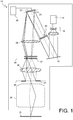
- FIG. 1 shows an illumination system 10 of a microlithographic projection exposure apparatus in a highly simplified meridian section.
- the illumination system 10 is used for suitably illuminating a mask 12, which carries lithographic structures to be imaged.
- a mask 12 which carries lithographic structures to be imaged.
- maximally uniform illumination of the mask 12 with projection light is desired so that the structures on the mask 12 can be transferred as uniformly as possible onto a wafer coated with a resist.
- the illumination angle distribution of the projection light is intended to mean the distribution, between the different incidence angles at which the light strikes the mask point, of the total intensity of the light striking a mask point.
- the illumination system 10 comprises a multiplicity of optical elements in its beam path, which in Figure 1 are mostly represented only in a highly simplified way or not at all.
- the projection light generated by a laser 14 or another light source is initially expanded by first optics 16 and directed by means of a plane mirror 18 onto a microlens array 20.
- the plane mirror 18 is primarily used to keep the external dimensions of the illumination system 10 compact.
- the multi-mirror array 22 comprises a multiplicity of micromirrors 24 which can be tilted, preferably individually, by means of a drive instrument 26.
- the upstream microlens array 20 focuses individual light sub-beams of the projection light onto the micromirrors 24.
- the individual micromirrors 24 can be tilted so that the light sub-beams of the projection light pass, via second optics 28, through a pupil surface 30 at freely selectable positions.
- a fly's eye integrator 32 arranged near this pupil surface 30 generates a multiplicity of secondary light sources in the pupil surface 30, which, via a third optics 34, uniformly illuminate an intermediate field plane 35 in which adjustable stop elements 37 are arranged.
- the third optics 34 generate an assignment between angles in the pupil surface 30 and positions in the intermediate field plane 35.
- the latter is imaged by an objective 36 onto a mask plane, in which the mask 12 is arranged.
- the intensity distribution in the pupil surface 30 therefore determines the illumination angle distribution not only in the intermediate field plane 35 but also in the mask plane.
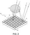
- FIG. 2 shows a simplified perspective representation of the multi-mirror array 22, in which the individual micromirrors 24 are plane and have a square contour.
- each micromirror 24 is mounted tiltably about two tilt axes x and y.
- the tilting per se about the tilt axes x, y can be controlled by means of actuators, and each micromirror 24 should if possible be assigned its own set of actuators so that the micromirrors 24 can be driven individually. Therefore, each micromirror 24 with the associated actuators thus forms a mirror unit 38 which is repeated over the multi-mirror array 22.
- Multi-mirror arrays 22 having several thousand micromirrors 24, tiltable about two tilt axes x, y, may be envisaged. Such multi-mirror arrays 22 may, for example, be fabricated in MEMS technology.
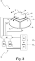
- FIG 3 shows a highly schematised perspective representation of an embodiment of a mirror unit 38 in which, unlike in the embodiment shown in Figure 2 , the micromirror 24 has a circular contour.
- Drive electronics which are part of the drive instrument 26 and by which this micromirror 24 can be driven, are denoted by 39.
- the main component of the mirror unit 38 is the micromirror 24, which has a plane mirror support whose mirror surface 40 carries a coating which reflects the projection light being used, for example VUV light with a wavelength of 193 nm.
- the mirror surface 40 may be assigned a surface normal 42, with respect to which the incidence angle and emergence angle of the projection light striking the micromirror 24 can be defined. In the case of a curved mirror surface 40, an average surface normal 42 may be defined for this purpose.
- the micromirror 24 is mounted tiltably by means of a universal suspension (not shown) about the two tilt axes x and y, which are represented by dashes in Figure 3 .
- the universal suspension which allows two degrees of freedom in rotation, exerts a restoring moment on the micromirror 24 by means of resilient solid-state articulations used for supporting it, and thus keeps it in a stable central position.
- a mirror electrode 44 which is produced for example by vapour depositing a metallic layer, is applied on the rear side of the micromirror 24.
- a first control electrode E 1 , a second control electrode E 2 and a third control electrode E 3 which are configured as circular disc segments with a vertex angle of 120°, are applied opposite this mirror electrode 44, and therefore the entire micromirror 24, on the substrate of the mirror unit 38.
- the leads of the three control electrodes E 1 , E 2 and E 3 and the mirror electrode 44 are fed out from the MEMS unit and connected to the associated drive electronics 39.
- the mirror electrode 44 is pulled by the individual control electrodes E 1 , E 2 and E 3 owing to electrostatic attraction.
- This attractive force between the two electrodes is converted by the universal suspension into tilting of the micromirror 24 about the two tilt axes x and y.
- the control electrodes E 1 , E 2 and E 3 therefore function as actuators for tilting the micromirror 24.
- the respective tilt angle is essentially dictated by the interaction of the various voltages U 1 , U 2 and U 3 and the restoring moments established by the solid-state articulations of the universal suspension.
- Other forces which act on the micromirror 24, for example gravitational forces, may be neglected in this embodiment since the micromirror 24 is intended to be very small here. Forces due to effects such as for example housing vibrations, air flows or thermal effects may, however, have a considerable influence on the real setting of the micromirror 24.
- control variables SG x and SG y which are assigned, preferably linearly, to the desired unperturbed tilt angles ⁇ x and ⁇ y about the tilt axes x and y are transmitted to the drive electronics 39.
- the drive electronics 39 comprise a converter 46, a multiplexer 48 and two signal amplifiers in the form of two controllable high-voltage output stages 50 and 52.
- the converter 46 receives the two control variables SG x and SG y on two input lines and, by means of a memory 45 and/or a calculation unit 47, determines the values of the three voltages U 1 , U 2 and U 3 which are applied to the control electrodes E 1 , E 2 and E 3 .
- a function of the control variables SG x , SG y according to a method explained below with the aid of Figures 4 to 6 , one control electrode E 1 , E 2 or E 3 is respectively selected, for example the first control electrode E 1 , and its voltage U 1 relative to the mirror electrode 44 is set to zero by means of the multiplexer 48, i.e. it is placed at the same potential as the mirror electrode 44.
- the converter 46 sets the other two voltages U 2 and U 3 to values which cause desired tilting of the micromirror 24.
- the multiplexer 48 which receives these two voltages U 2 and U 3 and is in turn driven by the converter 46, sets the selected control electrode E 1 to zero and applies the associated voltages U 2 and U 3 to the other two control electrodes E 2 and E 3 .
- control signals which are formed here by the various voltages U 1 , U 2 and U 3 , may for example be generated by constant-current sources instead of the high-voltage output stages 50 and 52.
- the signals specified by the converter 46 may also be transmitted in purely digital form to the signal amplifiers being used, as is possible in the case of digital-analogue converters with an integrated power output stage.
- a control signal which is constant over a plurality of mirror units 38 of the multi-mirror array 22 may also be applied by means of the multiplexer 48. In this way, the number of signal amplifiers needed per mirror unit 38 is reduced on average over the multi-mirror array 22 in this case as well.
- the starting point of the method is the two control variables SG x and SG y , which are transmitted for example from the output of a control and regulation algorithm to the converter 46 and are assigned to desired angles, i.e. unperturbed tilt angles ⁇ x and ⁇ y of the micromirror 24 about the respective tilt axis x, y.
- the method must therefore be capable of determining as precisely as possible the voltages U 1 , U 2 and U 3 which cause the micro-mirror 24 to tilt into the corresponding unperturbed tilt angles ⁇ x and ⁇ y .
- the torques with which the control electrodes E 1 , E 2 and E 3 act on the micromirror 24 may be assumed to be proportional to the square of the respective voltage U 1 , U 2 and U 3 .
- the restoring moments caused by the solid-state articulations of the universal suspension, which are in equilibrium with these torques, are approximately proportional to the tilting of the micromirror 24 so long as movement takes place in the elastic range of the solid-state articulations.
- the proportionality constants of the restoring moments which are also referred to as rotational spring constants, may be set differently in the direction of the tilt axes x and y.
- e 1 (e 1x ,e 1y ) T
- e 2 (e 2x ,e 2y ) T
- These proportionality factors are therefore also influenced for example by different orientations or configurations of the control electrodes E 1 , E 2 and E 3 and the mirror electrode 44, but also by manufacturing tolerances during their production.
- Vectors respectively rotated through 120° may be set as e 1 , e 2 and e 3 for the case assumed here in which the control electrodes E 1 , E 2 and E 3 are positioned ideally with threefold symmetry and are identical.
- the entries of the matrix T which represent the model parameters p 1x , p 1y , p 2x , p 2y , p 3x , P 3y of the mirror unit 38, may be obtained either from design data or by means of a measurement method. An example of such a measurement method will be explained in more detail below.
- the vector with the squared voltages may at any time be replaced by arbitrary functions f i (U i ) in the model above.
- Equation System (2) has infinitely many solutions, which may partly be restricted by requiring the voltages U 1 , U 2 and U 3 to be greater than or equal to zero for the sake of simplicity, since the electrostatic attraction effect between two electrodes is independent of the polarity of the voltage being used and the high-voltage output stages 50, 52 can therefore be configured for a voltage range with only one polarity.
- Equation System (2) becomes uniquely solvable since there are now only two unknowns to be determined. For particular tilting of the micromirror 24 about the two tilt axes x and y, however, it is not possible to set any voltage U 1 , U 2 or U 3 to zero. For this reason, in a first step it is necessary to select the control electrode E 1 , E 2 and E 3 whose voltage U 1 , U 2 or U 3 can be set to zero.
- control variables SG x and SG y span a control variable space which is assigned to the space of the unperturbed tilt angles ⁇ x and ⁇ y about the tilt axes x and y.
- this assignment or coordinate transformation may be made in any desired way, the control variables SG x and SG y being assigned preferably independently of one another and linearly to their respective tilt angle.
- an identical assignment between the control variables SG x , SG y and the unperturbed tilt angles ⁇ x , ⁇ y is assumed.
- the coordinate axes of the two spaces therefore correspond to each other, as is indicated in Figure 4 .
- various combinations of control variables SG x , SG y can now be plotted as different control variable vectors SGV.
- control electrodes E 1 , E 2 and E 3 and effective tilt vectors w 1 , w 2 and w 3 assigned to them the effects of the control electrodes E 1 , E 2 and E 3 , which they have on the micromirror 24, may also be taken into account in this control variable space.
- the respective effective tilt vector w 1 , w 2 or w 3 of a control electrode E 1 , E 2 or E 3 is in this case given by the control variables SG x , SG y that are assigned to those unperturbed tilt angles ⁇ x , ⁇ y which the micromirror 24 adopts when only this control electrode E 1 , E 2 or E 3 is driven with a type of standard voltage.
- the effective tilt vectors w 1 , w 2 or w 3 therefore correspond to the entries, or more precisely the columns, of the matrix T, which represent the model parameters p 1x , p 1y , p 2x , p 2y , p 3x , p 3y of the mirror unit 38 in Equation (2).
- an alignment angle ⁇ between the first control electrode E 1 and the tilt axis y which is due for example to manufacturing tolerances, is therefore also taken into account.
- Equation (2) has previously been solved as shown in Figure 5 , with the additional constraint condition that the total force F z which acts on the mirror element 24 is kept constant.
- the constraint condition of keeping constant the total force F z on the micromirror 24 is omitted, and instead one of the three control electrodes E 1 , E 2 or E 3 is selected and its voltage U 1 , U 2 or U 3 is set to zero. Admittedly, this cannot exclude the possibility that the micromirror 24 will execute minor excursion movements in the direction perpendicular to the tilt axes. Such excursion movements, however, are generally not detrimental to the optical function since the excursion movements in the case of plane micromirrors 24 do not affect the directions in which the projection light is being deviated.
- the orientation of the control variable vector SGV with respect to the effective tilt vectors w 1 , w 2 or w 3 of the three control electrodes E 1 , E 2 and E 3 is determined.
- the equation ⁇ arctan S G y S G x may be used in order to determine the angle ⁇ , while taking the respective quadrant into account.
- the root in Equation (5) is to be understood as taking the root component by component.
- the upper part of Figure 6 illustrates the profile of the voltages U 1 (continuous), U 2 (dashed) und U 3 (dotted) and shows that with the method used here, inter alia lower maximum voltages are needed in order to achieve particular tilting, since the control electrode E 1 , E 2 or E 3 whose effective tilt vector w 1 , w 2 or w 3 contains a component that would oppose the control variable vector SGV is respectively set to zero.
- the working range of the high-voltage output stages 50, 52 can therefore be selected to be smaller, so that smaller quantisation stages for the individual voltages and concomitantly smaller errors can be achieved.
- the lower part of Figure 6 also shows the variation in the total force F z , which occurs in the method described here and leads to the excursion movements already mentioned above.
- a measurement method may be used for determining the model parameters p 1x , p 1y , p 2x , p 2y , p 3x , p 3y , i.e. the entries of the matrix T, in order to take into account process variations in the production of the mirror units 38.
- various voltages U 1 , U 2 and U 3 are applied and the tilt angles ⁇ x and ⁇ y resulting therefrom are measured.
- Equation (8) The model parameters p 1x , p 1y , p 2x , p 2y , p 3x , p 3y could not be determined with only one measurement, since the equation system of Equation (8) would not be sufficiently determined. With N measurement points, N ⁇ 3 being required, i.e.
- N 2 unperturbed tilt angles ⁇ x , ⁇ y within the angle ranges of the two tilt axes x, y are activated in a measurement run, and these are stored together with the voltages U 1 , U 2 and U 3 required for this in a table, preferably in an electronic memory.
- the N 2 measurement points are expediently distributed uniformly on an N x N grid inside the angle ranges of the two tilt axes x, y.
- the activation of the individual tilt angles may for example be carried out with the aid of a regulation algorithm, to which the measured tilt angles ⁇ x , ⁇ y are in turn supplied.
- the individual tilt angles of the measurement run may, however, also be activated only with a control algorithm in which the real tilt angles are merely measured and stored with the associated voltages U 1 , U 2 and U 3 in the table.
- the associated voltages U 1 , U 2 and U 3 can be read out during operation and applied to the control electrodes E 1 , E 2 and E 3 . Since the values of the voltages U 1 , U 2 and U 3 are available only at the positions of the N x N tilt angles ⁇ x , ⁇ y , intermediate values may be calculated by interpolation, for example bilinearly or bicubically.
- FIG. 7 shows a diagram of the control and regulation system 54 as part of the drive instrument 26, the various components of which may be embodied individually as devices.
- the functions of the control and regulation algorithm 54 are undertaken by digital algorithms, which are carried out for example in a digital signal processor (DSP).
- DSP digital signal processor
- comments below about various components are also intended to refer to embodiments in the form of algorithms.
- Various embodiments may optionally contain only individual parts of these control and regulation components.
- the regulation section represented by dashes, which acts on the perturbation z, comprises the mirror unit 38 including the micromirror 24 and the associated drive electronics 39. If a linear, preferably identical assignment has been selected for assigning the control variables SG X , SG Y to the unperturbed tilt angles ⁇ x , ⁇ y of the micromirror 24 about the two tilt axes x, y, then, owing to the drive electronics 39, the considerations about the control and regulation components remain free from the complex dependencies of the unperturbed tilt angles ⁇ x , ⁇ y on the three control signals of the actuators, which are applied here in the form of voltages U 1 , U 2 and U 3 to the control electrodes E 1 , E 2 and E 3 of the mirror unit 38. The logic of the control and regulation components is therefore kept straightforward, which inter alia simplifies their layout.
- a trajectory determination unit 56 receives the target angle, through which the micromirror 24 is finally intended to be tilted, from a superordinate system or the user. From these target tilt angles, the trajectory determination unit 56 then determines a sequence of a setpoint tilt angles which converts the actual tilt angles, through which the micromirror 24 is instantaneously tilted, into the target tilt angles. This allows, for example, smooth activation of the target tilt angles. Calibration data, which can be used in order to adapt the actual tilt angles with respect to superordinate systems, may furthermore be transmitted to the trajectory determination unit 56.
- the sequence of setpoint tilt angles is transmitted to a regulator 58 that determines or corrects the control variables SG X , SG Y , which are transmitted to the drive electronics 39 of the mirror unit 38.
- the regulator 58 uses a regulation difference e, which is given by the setpoint tilt angles at the instant in question and negative feedback of the actual tilt angles measured by a monitoring system 60.
- a regulator 58 configured as a simple PID regulator may be parameterised according to the regulation characteristics of the regulation section.
- a predictive controller 62 is furthermore provided in the present embodiment, which contains an inverse system dynamics model of the regulation section and thus anticipates the reaction of the micromirror 24 to a change in the control variables SG X , SG Y .
- Such a solution is recommendable in particular owing to the multiplicity of individual mirror units 38, since the regulation frequency of the closed control loop via the regulator 58, dictated essentially by the limited bandwidth of the monitoring system 60, may be relatively low.
- the predictive controller 62 therefore comprises the predictable reaction of the control section, and the regulator 58 corrects the control variables SG X , SG Y specified by the predictive controller 62 in order to compensate for the perturbation z acting on the control section and errors of the drive electronics 39.
- control variables SG X , SG Y thus determined and optionally corrected are then converted by the drive electronics 39 into control signals according to the method presented above, and these are applied to the actuators of the mirror unit 38.
- All the described methods and devices for driving a micro-mirror 24 in a multi-mirror array 22 may also be employed in illumination systems for the use of EUV light, i.e. light with a wavelength in the range of a few nanometres, for example 13.6 nm.
Landscapes
- Physics & Mathematics (AREA)
- General Physics & Mathematics (AREA)
- Optics & Photonics (AREA)
- Spectroscopy & Molecular Physics (AREA)
- Mechanical Light Control Or Optical Switches (AREA)
- Exposure And Positioning Against Photoresist Photosensitive Materials (AREA)
- Exposure Of Semiconductors, Excluding Electron Or Ion Beam Exposure (AREA)
- Micromachines (AREA)
- Non-Portable Lighting Devices Or Systems Thereof (AREA)
Applications Claiming Priority (4)
| Application Number | Priority Date | Filing Date | Title |
|---|---|---|---|
| US10369108P | 2008-10-08 | 2008-10-08 | |
| DE102008050446A DE102008050446B4 (de) | 2008-10-08 | 2008-10-08 | Verfahren und Vorrichtungen zur Ansteuerung von Mikrospiegeln |
| PCT/EP2009/007175 WO2010040506A1 (en) | 2008-10-08 | 2009-10-06 | Methods and devices for driving micromirrors |
| EP09744324.6A EP2340456B1 (en) | 2008-10-08 | 2009-10-06 | Methods and devices for driving micromirrors |
Related Parent Applications (1)
| Application Number | Title | Priority Date | Filing Date |
|---|---|---|---|
| EP09744324.6A Division EP2340456B1 (en) | 2008-10-08 | 2009-10-06 | Methods and devices for driving micromirrors |
Publications (2)
| Publication Number | Publication Date |
|---|---|
| EP3193203A1 EP3193203A1 (en) | 2017-07-19 |
| EP3193203B1 true EP3193203B1 (en) | 2018-08-29 |
Family
ID=41821122
Family Applications (2)
| Application Number | Title | Priority Date | Filing Date |
|---|---|---|---|
| EP17157830.5A Active EP3193203B1 (en) | 2008-10-08 | 2009-10-06 | Methods and devices for driving micromirrors |
| EP09744324.6A Active EP2340456B1 (en) | 2008-10-08 | 2009-10-06 | Methods and devices for driving micromirrors |
Family Applications After (1)
| Application Number | Title | Priority Date | Filing Date |
|---|---|---|---|
| EP09744324.6A Active EP2340456B1 (en) | 2008-10-08 | 2009-10-06 | Methods and devices for driving micromirrors |
Country Status (8)
| Country | Link |
|---|---|
| US (2) | US8345224B2 (enExample) |
| EP (2) | EP3193203B1 (enExample) |
| JP (1) | JP5325301B2 (enExample) |
| KR (1) | KR101233900B1 (enExample) |
| CN (2) | CN104267495B (enExample) |
| DE (1) | DE102008050446B4 (enExample) |
| TW (1) | TWI502282B (enExample) |
| WO (1) | WO2010040506A1 (enExample) |
Families Citing this family (26)
| Publication number | Priority date | Publication date | Assignee | Title |
|---|---|---|---|---|
| DE102008050446B4 (de) | 2008-10-08 | 2011-07-28 | Carl Zeiss SMT GmbH, 73447 | Verfahren und Vorrichtungen zur Ansteuerung von Mikrospiegeln |
| CN102349026B (zh) | 2009-03-13 | 2015-07-29 | 卡尔蔡司Smt有限责任公司 | 微光刻投射曝光设备 |
| DE102010062720B4 (de) | 2010-12-09 | 2012-07-12 | Carl Zeiss Smt Gmbh | EUV-Lithographiesystem |
| WO2012169089A1 (ja) | 2011-06-07 | 2012-12-13 | 株式会社ニコン | 照明光学系、露光装置、デバイス製造方法、および偏光ユニット |
| TWI587002B (zh) | 2011-06-13 | 2017-06-11 | 尼康股份有限公司 | 照明方法 |
| WO2013061858A1 (ja) | 2011-10-24 | 2013-05-02 | 株式会社ニコン | 照明光学系、露光装置、およびデバイス製造方法 |
| US9732934B2 (en) | 2011-10-28 | 2017-08-15 | Nikon Corporation | Illumination device for optimizing polarization in an illumination pupil |
| JP5918858B2 (ja) | 2011-11-15 | 2016-05-18 | カール・ツァイス・エスエムティー・ゲーエムベーハー | マイクロリソグラフィ投影露光装置の光変調器及び照明系 |
| DE102013201506A1 (de) | 2012-02-17 | 2013-08-22 | Carl Zeiss Smt Gmbh | Optisches Bauelement |
| DE102013201509A1 (de) | 2012-02-17 | 2013-08-22 | Carl Zeiss Smt Gmbh | Optisches Bauelement |
| JPWO2013164997A1 (ja) | 2012-05-02 | 2015-12-24 | 株式会社ニコン | 瞳輝度分布の評価方法および改善方法、照明光学系およびその調整方法、露光装置、露光方法、並びにデバイス製造方法 |
| DE102012011202A1 (de) * | 2012-06-06 | 2013-09-12 | Carl Zeiss Smt Gmbh | Projektor und Verfahren zum Erzeugen eines Bildes |
| JP6246907B2 (ja) * | 2013-05-22 | 2017-12-13 | カール・ツァイス・エスエムティー・ゲーエムベーハー | 光学素子及び当該光学素子に対する放射の影響を低減する手段を備えた光学コンポーネント |
| DE102013212613B4 (de) * | 2013-06-28 | 2015-07-23 | Carl Zeiss Sms Gmbh | Beleuchtungsoptik für ein Metrologiesystem sowie Metrologiesystem mit einer derartigen Beleuchtungsoptik |
| JP6273109B2 (ja) * | 2013-08-28 | 2018-01-31 | 株式会社ミツトヨ | 光干渉測定装置 |
| DE102014203188A1 (de) * | 2014-02-21 | 2015-08-27 | Carl Zeiss Smt Gmbh | Verfahren zur Beleuchtung eines Objektfeldes einer Projektionsbelichtungsanlage |
| CN104111592B (zh) * | 2014-08-06 | 2016-06-08 | 中国科学院光电技术研究所 | 一种基于微反射镜阵列实现可变自由照明光瞳的方法 |
| CN105573061B (zh) * | 2014-10-16 | 2018-03-06 | 中芯国际集成电路制造(上海)有限公司 | Euv光源和曝光装置 |
| DE102017217164B4 (de) | 2017-09-27 | 2020-10-15 | Continental Automotive Gmbh | Projektionsvorrichtung zum Erzeugen eines pixelbasierten Beleuchtungsmusters |
| DE102018202421B3 (de) | 2018-02-16 | 2019-07-11 | Carl Zeiss Microscopy Gmbh | Vielstrahl-Teilchenstrahlsystem |
| DE102018216344A1 (de) * | 2018-09-25 | 2020-03-26 | Carl Zeiss Smt Gmbh | Abstützung eines optischen elements |
| CN110347082B (zh) * | 2019-07-12 | 2021-07-27 | 中国科学院上海微系统与信息技术研究所 | 一种驱动电路、驱动方法及微反射镜阵列 |
| CN110954142B (zh) * | 2019-12-10 | 2021-12-28 | 京东方科技集团股份有限公司 | 一种光学微电机传感器、基板及电子设备 |
| CN114660880A (zh) * | 2022-04-11 | 2022-06-24 | 长沙沃默科技有限公司 | 一种反射式投影成像装置及其设计方法 |
| CN116698367A (zh) * | 2023-05-23 | 2023-09-05 | 上海镭望光学科技有限公司 | 微反射镜阵列反射光光斑位置标定方法、装置及标定设备 |
| DE102023207368A1 (de) * | 2023-08-01 | 2025-02-06 | Carl Zeiss Smt Gmbh | Ansteuervorrichtung, optisches system und lithographieanlage |
Family Cites Families (31)
| Publication number | Priority date | Publication date | Assignee | Title |
|---|---|---|---|---|
| US6312134B1 (en) * | 1996-07-25 | 2001-11-06 | Anvik Corporation | Seamless, maskless lithography system using spatial light modulator |
| JP2863502B2 (ja) * | 1996-10-23 | 1999-03-03 | 防衛庁技術研究本部長 | マルチディザー方式補償光学装置 |
| US7006595B2 (en) * | 1998-05-05 | 2006-02-28 | Carl Zeiss Semiconductor Manufacturing Technologies Ag | Illumination system particularly for microlithography |
| KR100716946B1 (ko) | 2000-07-20 | 2007-05-10 | 삼성전자주식회사 | 마이크로미러 액추에이터를 이용한 광결합 구조체 |
| KR100332888B1 (ko) | 2000-08-25 | 2002-04-15 | 이형도 | 마이크로 미러를 이용한 광 픽업 액츄에이터 |
| US6300665B1 (en) | 2000-09-28 | 2001-10-09 | Xerox Corporation | Structure for an optical switch on a silicon on insulator substrate |
| JP2002189176A (ja) * | 2000-12-20 | 2002-07-05 | Mitsubishi Electric Corp | ミラー駆動装置 |
| KR100389865B1 (ko) * | 2001-03-02 | 2003-07-04 | 삼성전자주식회사 | 마이크로미러 디바이스 및 이를 채용한 프로젝터 |
| US6735004B1 (en) * | 2001-03-15 | 2004-05-11 | Nanogear, Inc. | Rotatable counterbalanced actuator |
| JP3724432B2 (ja) * | 2001-04-19 | 2005-12-07 | 株式会社ニコン | 薄膜弾性構造体及びその製造方法並びにこれを用いたミラーデバイス及び光スイッチ |
| JP3908503B2 (ja) * | 2001-10-30 | 2007-04-25 | 富士通株式会社 | 光スイッチ |
| US6643053B2 (en) * | 2002-02-20 | 2003-11-04 | The Regents Of The University Of California | Piecewise linear spatial phase modulator using dual-mode micromirror arrays for temporal and diffractive fourier optics |
| US6717325B2 (en) * | 2002-03-06 | 2004-04-06 | Glimmerglass Networks, Inc. | Method and apparatus for actuation of a two-axis MEMS device using three actuation elements |
| US6707534B2 (en) * | 2002-05-10 | 2004-03-16 | Anvik Corporation | Maskless conformable lithography |
| EP1367446A1 (en) * | 2002-05-31 | 2003-12-03 | ASML Netherlands B.V. | Lithographic apparatus |
| KR100464320B1 (ko) * | 2002-11-19 | 2004-12-31 | 삼성전자주식회사 | 마이크로미러 액츄에이터 및 그 제조방법 |
| US6906848B2 (en) * | 2003-02-24 | 2005-06-14 | Exajoule, Llc | Micromirror systems with concealed multi-piece hinge structures |
| JP4244156B2 (ja) * | 2003-05-07 | 2009-03-25 | 富士フイルム株式会社 | 投影露光装置 |
| JP4357317B2 (ja) * | 2003-05-13 | 2009-11-04 | 富士通株式会社 | ティルトミラーの制御装置及び制御方法 |
| US7714983B2 (en) * | 2003-09-12 | 2010-05-11 | Carl Zeiss Smt Ag | Illumination system for a microlithography projection exposure installation |
| DE10343333A1 (de) * | 2003-09-12 | 2005-04-14 | Carl Zeiss Smt Ag | Beleuchtungssystem für eine Mikrolithographie-Projektionsbelichtungsanlage |
| US7646528B2 (en) * | 2006-12-26 | 2010-01-12 | Silicon Quest Kabushiki-Kaisha | Deformable mirror device with oscillating states |
| US7304783B2 (en) * | 2003-11-01 | 2007-12-04 | Fusao Ishii | Control of micromirrors with intermediate states |
| WO2005085125A1 (ja) * | 2004-03-08 | 2005-09-15 | Matsushita Electric Industrial Co., Ltd. | マイクロアクチュエータ、およびマイクロアクチュエータを備えた装置 |
| US7855825B2 (en) | 2005-04-15 | 2010-12-21 | Panasonic Corporation | Micromachine structure system and method for manufacturing same |
| JP2007264305A (ja) * | 2006-03-28 | 2007-10-11 | Fujitsu Ltd | 光スイッチシステム |
| DE102006020734A1 (de) * | 2006-05-04 | 2007-11-15 | Carl Zeiss Smt Ag | Beleuchtungssystem für die EUV-Lithographie sowie erstes und zweites optisches Element zum Einsatz in einem derartigen Beleuchtungssystem |
| US9250536B2 (en) * | 2007-03-30 | 2016-02-02 | Asml Netherlands B.V. | Lithographic apparatus and method |
| CN101796460B (zh) * | 2007-08-30 | 2013-05-01 | 卡尔蔡司Smt有限责任公司 | 微光刻投射曝光设备中用于照明掩模的照明系统 |
| CN103034075B (zh) * | 2007-12-21 | 2015-07-08 | 卡尔蔡司Smt有限责任公司 | 微光刻投射曝光设备的照明系统 |
| DE102008050446B4 (de) | 2008-10-08 | 2011-07-28 | Carl Zeiss SMT GmbH, 73447 | Verfahren und Vorrichtungen zur Ansteuerung von Mikrospiegeln |
-
2008
- 2008-10-08 DE DE102008050446A patent/DE102008050446B4/de active Active
-
2009
- 2009-10-06 EP EP17157830.5A patent/EP3193203B1/en active Active
- 2009-10-06 WO PCT/EP2009/007175 patent/WO2010040506A1/en not_active Ceased
- 2009-10-06 KR KR1020117010412A patent/KR101233900B1/ko active Active
- 2009-10-06 JP JP2011530409A patent/JP5325301B2/ja active Active
- 2009-10-06 CN CN201410453043.5A patent/CN104267495B/zh active Active
- 2009-10-06 CN CN2009801398210A patent/CN102177460A/zh active Pending
- 2009-10-06 EP EP09744324.6A patent/EP2340456B1/en active Active
- 2009-10-07 TW TW098133956A patent/TWI502282B/zh active
-
2011
- 2011-03-02 US US13/038,734 patent/US8345224B2/en active Active
-
2012
- 2012-11-28 US US13/687,887 patent/US10061202B2/en active Active
Also Published As
| Publication number | Publication date |
|---|---|
| JP5325301B2 (ja) | 2013-10-23 |
| KR101233900B1 (ko) | 2013-02-15 |
| DE102008050446A1 (de) | 2010-04-15 |
| CN104267495A (zh) | 2015-01-07 |
| TW201019051A (en) | 2010-05-16 |
| CN102177460A (zh) | 2011-09-07 |
| KR20110067156A (ko) | 2011-06-21 |
| US20130088698A1 (en) | 2013-04-11 |
| US20110188017A1 (en) | 2011-08-04 |
| TWI502282B (zh) | 2015-10-01 |
| JP2012505533A (ja) | 2012-03-01 |
| EP2340456A1 (en) | 2011-07-06 |
| CN104267495B (zh) | 2016-12-07 |
| DE102008050446B4 (de) | 2011-07-28 |
| US8345224B2 (en) | 2013-01-01 |
| WO2010040506A1 (en) | 2010-04-15 |
| EP3193203A1 (en) | 2017-07-19 |
| EP2340456B1 (en) | 2017-04-05 |
| US10061202B2 (en) | 2018-08-28 |
Similar Documents
| Publication | Publication Date | Title |
|---|---|---|
| EP3193203B1 (en) | Methods and devices for driving micromirrors | |
| JP5639894B2 (ja) | マイクロリソグラフィ投影露光装置用の照明系 | |
| JP5727005B2 (ja) | 光学系及びマルチファセットミラー | |
| US10514619B2 (en) | Sensor arrangement for a lithography system, lithography system, and method for operating a lithography system | |
| JP2016177292A (ja) | マイクロリソグラフィ投影露光装置の素子を作動させる機構 | |
| US9851554B2 (en) | Method for displacing at least one optical component | |
| KR20130108279A (ko) | 마이크로리소그래피 투영 노광 장치 | |
| WO2014012643A2 (en) | System correction from long timescales | |
| KR100714468B1 (ko) | 리소그래피 장치, 제어 시스템 및 디바이스 제조방법 | |
| CN121153008A (zh) | 用于操作微光刻投射曝光设备中的固态致动器的方法 | |
| EP1616211B1 (en) | Exposure Control |
Legal Events
| Date | Code | Title | Description |
|---|---|---|---|
| PUAI | Public reference made under article 153(3) epc to a published international application that has entered the european phase |
Free format text: ORIGINAL CODE: 0009012 |
|
| STAA | Information on the status of an ep patent application or granted ep patent |
Free format text: STATUS: THE APPLICATION HAS BEEN PUBLISHED |
|
| AC | Divisional application: reference to earlier application |
Ref document number: 2340456 Country of ref document: EP Kind code of ref document: P |
|
| AK | Designated contracting states |
Kind code of ref document: A1 Designated state(s): AT BE BG CH CY CZ DE DK EE ES FI FR GB GR HR HU IE IS IT LI LT LU LV MC MK MT NL NO PL PT RO SE SI SK SM TR |
|
| STAA | Information on the status of an ep patent application or granted ep patent |
Free format text: STATUS: REQUEST FOR EXAMINATION WAS MADE |
|
| 17P | Request for examination filed |
Effective date: 20171206 |
|
| RBV | Designated contracting states (corrected) |
Designated state(s): AT BE BG CH CY CZ DE DK EE ES FI FR GB GR HR HU IE IS IT LI LT LU LV MC MK MT NL NO PL PT RO SE SI SK SM TR |
|
| GRAP | Despatch of communication of intention to grant a patent |
Free format text: ORIGINAL CODE: EPIDOSNIGR1 |
|
| STAA | Information on the status of an ep patent application or granted ep patent |
Free format text: STATUS: GRANT OF PATENT IS INTENDED |
|
| INTG | Intention to grant announced |
Effective date: 20180322 |
|
| GRAS | Grant fee paid |
Free format text: ORIGINAL CODE: EPIDOSNIGR3 |
|
| GRAA | (expected) grant |
Free format text: ORIGINAL CODE: 0009210 |
|
| STAA | Information on the status of an ep patent application or granted ep patent |
Free format text: STATUS: THE PATENT HAS BEEN GRANTED |
|
| AC | Divisional application: reference to earlier application |
Ref document number: 2340456 Country of ref document: EP Kind code of ref document: P |
|
| AK | Designated contracting states |
Kind code of ref document: B1 Designated state(s): AT BE BG CH CY CZ DE DK EE ES FI FR GB GR HR HU IE IS IT LI LT LU LV MC MK MT NL NO PL PT RO SE SI SK SM TR |
|
| REG | Reference to a national code |
Ref country code: GB Ref legal event code: FG4D |
|
| REG | Reference to a national code |
Ref country code: CH Ref legal event code: EP |
|
| REG | Reference to a national code |
Ref country code: AT Ref legal event code: REF Ref document number: 1035802 Country of ref document: AT Kind code of ref document: T Effective date: 20180915 |
|
| REG | Reference to a national code |
Ref country code: IE Ref legal event code: FG4D |
|
| REG | Reference to a national code |
Ref country code: DE Ref legal event code: R096 Ref document number: 602009054244 Country of ref document: DE |
|
| REG | Reference to a national code |
Ref country code: NL Ref legal event code: FP |
|
| REG | Reference to a national code |
Ref country code: LT Ref legal event code: MG4D |
|
| PG25 | Lapsed in a contracting state [announced via postgrant information from national office to epo] |
Ref country code: NO Free format text: LAPSE BECAUSE OF FAILURE TO SUBMIT A TRANSLATION OF THE DESCRIPTION OR TO PAY THE FEE WITHIN THE PRESCRIBED TIME-LIMIT Effective date: 20181129 Ref country code: BG Free format text: LAPSE BECAUSE OF FAILURE TO SUBMIT A TRANSLATION OF THE DESCRIPTION OR TO PAY THE FEE WITHIN THE PRESCRIBED TIME-LIMIT Effective date: 20181129 Ref country code: SE Free format text: LAPSE BECAUSE OF FAILURE TO SUBMIT A TRANSLATION OF THE DESCRIPTION OR TO PAY THE FEE WITHIN THE PRESCRIBED TIME-LIMIT Effective date: 20180829 Ref country code: FI Free format text: LAPSE BECAUSE OF FAILURE TO SUBMIT A TRANSLATION OF THE DESCRIPTION OR TO PAY THE FEE WITHIN THE PRESCRIBED TIME-LIMIT Effective date: 20180829 Ref country code: GR Free format text: LAPSE BECAUSE OF FAILURE TO SUBMIT A TRANSLATION OF THE DESCRIPTION OR TO PAY THE FEE WITHIN THE PRESCRIBED TIME-LIMIT Effective date: 20181130 Ref country code: LT Free format text: LAPSE BECAUSE OF FAILURE TO SUBMIT A TRANSLATION OF THE DESCRIPTION OR TO PAY THE FEE WITHIN THE PRESCRIBED TIME-LIMIT Effective date: 20180829 Ref country code: IS Free format text: LAPSE BECAUSE OF FAILURE TO SUBMIT A TRANSLATION OF THE DESCRIPTION OR TO PAY THE FEE WITHIN THE PRESCRIBED TIME-LIMIT Effective date: 20181229 |
|
| REG | Reference to a national code |
Ref country code: AT Ref legal event code: MK05 Ref document number: 1035802 Country of ref document: AT Kind code of ref document: T Effective date: 20180829 |
|
| PG25 | Lapsed in a contracting state [announced via postgrant information from national office to epo] |
Ref country code: HR Free format text: LAPSE BECAUSE OF FAILURE TO SUBMIT A TRANSLATION OF THE DESCRIPTION OR TO PAY THE FEE WITHIN THE PRESCRIBED TIME-LIMIT Effective date: 20180829 Ref country code: LV Free format text: LAPSE BECAUSE OF FAILURE TO SUBMIT A TRANSLATION OF THE DESCRIPTION OR TO PAY THE FEE WITHIN THE PRESCRIBED TIME-LIMIT Effective date: 20180829 |
|
| PG25 | Lapsed in a contracting state [announced via postgrant information from national office to epo] |
Ref country code: EE Free format text: LAPSE BECAUSE OF FAILURE TO SUBMIT A TRANSLATION OF THE DESCRIPTION OR TO PAY THE FEE WITHIN THE PRESCRIBED TIME-LIMIT Effective date: 20180829 Ref country code: PL Free format text: LAPSE BECAUSE OF FAILURE TO SUBMIT A TRANSLATION OF THE DESCRIPTION OR TO PAY THE FEE WITHIN THE PRESCRIBED TIME-LIMIT Effective date: 20180829 Ref country code: RO Free format text: LAPSE BECAUSE OF FAILURE TO SUBMIT A TRANSLATION OF THE DESCRIPTION OR TO PAY THE FEE WITHIN THE PRESCRIBED TIME-LIMIT Effective date: 20180829 Ref country code: IT Free format text: LAPSE BECAUSE OF FAILURE TO SUBMIT A TRANSLATION OF THE DESCRIPTION OR TO PAY THE FEE WITHIN THE PRESCRIBED TIME-LIMIT Effective date: 20180829 Ref country code: CZ Free format text: LAPSE BECAUSE OF FAILURE TO SUBMIT A TRANSLATION OF THE DESCRIPTION OR TO PAY THE FEE WITHIN THE PRESCRIBED TIME-LIMIT Effective date: 20180829 Ref country code: AT Free format text: LAPSE BECAUSE OF FAILURE TO SUBMIT A TRANSLATION OF THE DESCRIPTION OR TO PAY THE FEE WITHIN THE PRESCRIBED TIME-LIMIT Effective date: 20180829 Ref country code: ES Free format text: LAPSE BECAUSE OF FAILURE TO SUBMIT A TRANSLATION OF THE DESCRIPTION OR TO PAY THE FEE WITHIN THE PRESCRIBED TIME-LIMIT Effective date: 20180829 |
|
| PG25 | Lapsed in a contracting state [announced via postgrant information from national office to epo] |
Ref country code: SK Free format text: LAPSE BECAUSE OF FAILURE TO SUBMIT A TRANSLATION OF THE DESCRIPTION OR TO PAY THE FEE WITHIN THE PRESCRIBED TIME-LIMIT Effective date: 20180829 Ref country code: DK Free format text: LAPSE BECAUSE OF FAILURE TO SUBMIT A TRANSLATION OF THE DESCRIPTION OR TO PAY THE FEE WITHIN THE PRESCRIBED TIME-LIMIT Effective date: 20180829 Ref country code: SM Free format text: LAPSE BECAUSE OF FAILURE TO SUBMIT A TRANSLATION OF THE DESCRIPTION OR TO PAY THE FEE WITHIN THE PRESCRIBED TIME-LIMIT Effective date: 20180829 |
|
| REG | Reference to a national code |
Ref country code: CH Ref legal event code: PL Ref country code: DE Ref legal event code: R097 Ref document number: 602009054244 Country of ref document: DE |
|
| REG | Reference to a national code |
Ref country code: BE Ref legal event code: MM Effective date: 20181031 |
|
| PG25 | Lapsed in a contracting state [announced via postgrant information from national office to epo] |
Ref country code: LU Free format text: LAPSE BECAUSE OF NON-PAYMENT OF DUE FEES Effective date: 20181006 Ref country code: MC Free format text: LAPSE BECAUSE OF FAILURE TO SUBMIT A TRANSLATION OF THE DESCRIPTION OR TO PAY THE FEE WITHIN THE PRESCRIBED TIME-LIMIT Effective date: 20180829 |
|
| PLBE | No opposition filed within time limit |
Free format text: ORIGINAL CODE: 0009261 |
|
| STAA | Information on the status of an ep patent application or granted ep patent |
Free format text: STATUS: NO OPPOSITION FILED WITHIN TIME LIMIT |
|
| GBPC | Gb: european patent ceased through non-payment of renewal fee |
Effective date: 20181129 |
|
| REG | Reference to a national code |
Ref country code: IE Ref legal event code: MM4A |
|
| 26N | No opposition filed |
Effective date: 20190531 |
|
| PG25 | Lapsed in a contracting state [announced via postgrant information from national office to epo] |
Ref country code: BE Free format text: LAPSE BECAUSE OF NON-PAYMENT OF DUE FEES Effective date: 20181031 Ref country code: FR Free format text: LAPSE BECAUSE OF NON-PAYMENT OF DUE FEES Effective date: 20181029 Ref country code: SI Free format text: LAPSE BECAUSE OF FAILURE TO SUBMIT A TRANSLATION OF THE DESCRIPTION OR TO PAY THE FEE WITHIN THE PRESCRIBED TIME-LIMIT Effective date: 20180829 Ref country code: LI Free format text: LAPSE BECAUSE OF NON-PAYMENT OF DUE FEES Effective date: 20181031 Ref country code: CH Free format text: LAPSE BECAUSE OF NON-PAYMENT OF DUE FEES Effective date: 20181031 |
|
| PG25 | Lapsed in a contracting state [announced via postgrant information from national office to epo] |
Ref country code: IE Free format text: LAPSE BECAUSE OF NON-PAYMENT OF DUE FEES Effective date: 20181006 |
|
| PG25 | Lapsed in a contracting state [announced via postgrant information from national office to epo] |
Ref country code: GB Free format text: LAPSE BECAUSE OF NON-PAYMENT OF DUE FEES Effective date: 20181129 |
|
| PG25 | Lapsed in a contracting state [announced via postgrant information from national office to epo] |
Ref country code: MT Free format text: LAPSE BECAUSE OF NON-PAYMENT OF DUE FEES Effective date: 20181006 |
|
| PG25 | Lapsed in a contracting state [announced via postgrant information from national office to epo] |
Ref country code: TR Free format text: LAPSE BECAUSE OF FAILURE TO SUBMIT A TRANSLATION OF THE DESCRIPTION OR TO PAY THE FEE WITHIN THE PRESCRIBED TIME-LIMIT Effective date: 20180829 |
|
| PG25 | Lapsed in a contracting state [announced via postgrant information from national office to epo] |
Ref country code: PT Free format text: LAPSE BECAUSE OF FAILURE TO SUBMIT A TRANSLATION OF THE DESCRIPTION OR TO PAY THE FEE WITHIN THE PRESCRIBED TIME-LIMIT Effective date: 20180829 |
|
| PG25 | Lapsed in a contracting state [announced via postgrant information from national office to epo] |
Ref country code: MK Free format text: LAPSE BECAUSE OF NON-PAYMENT OF DUE FEES Effective date: 20180829 Ref country code: HU Free format text: LAPSE BECAUSE OF FAILURE TO SUBMIT A TRANSLATION OF THE DESCRIPTION OR TO PAY THE FEE WITHIN THE PRESCRIBED TIME-LIMIT; INVALID AB INITIO Effective date: 20091006 Ref country code: CY Free format text: LAPSE BECAUSE OF FAILURE TO SUBMIT A TRANSLATION OF THE DESCRIPTION OR TO PAY THE FEE WITHIN THE PRESCRIBED TIME-LIMIT Effective date: 20180829 |
|
| P01 | Opt-out of the competence of the unified patent court (upc) registered |
Effective date: 20230525 |
|
| PGFP | Annual fee paid to national office [announced via postgrant information from national office to epo] |
Ref country code: DE Payment date: 20241021 Year of fee payment: 16 |
|
| PGFP | Annual fee paid to national office [announced via postgrant information from national office to epo] |
Ref country code: NL Payment date: 20251021 Year of fee payment: 17 |