EP3173849A1 - Light source optical system and projection display apparatus employing the same - Google Patents
Light source optical system and projection display apparatus employing the same Download PDFInfo
- Publication number
- EP3173849A1 EP3173849A1 EP16199961.0A EP16199961A EP3173849A1 EP 3173849 A1 EP3173849 A1 EP 3173849A1 EP 16199961 A EP16199961 A EP 16199961A EP 3173849 A1 EP3173849 A1 EP 3173849A1
- Authority
- EP
- European Patent Office
- Prior art keywords
- light
- light source
- optical system
- light flux
- lens
- Prior art date
- Legal status (The legal status is an assumption and is not a legal conclusion. Google has not performed a legal analysis and makes no representation as to the accuracy of the status listed.)
- Withdrawn
Links
Images


Classifications
-
- G—PHYSICS
- G02—OPTICS
- G02B—OPTICAL ELEMENTS, SYSTEMS OR APPARATUS
- G02B27/00—Optical systems or apparatus not provided for by any of the groups G02B1/00 - G02B26/00, G02B30/00
- G02B27/10—Beam splitting or combining systems
-
- G—PHYSICS
- G02—OPTICS
- G02B—OPTICAL ELEMENTS, SYSTEMS OR APPARATUS
- G02B27/00—Optical systems or apparatus not provided for by any of the groups G02B1/00 - G02B26/00, G02B30/00
- G02B27/10—Beam splitting or combining systems
- G02B27/14—Beam splitting or combining systems operating by reflection only
- G02B27/141—Beam splitting or combining systems operating by reflection only using dichroic mirrors
-
- G—PHYSICS
- G03—PHOTOGRAPHY; CINEMATOGRAPHY; ANALOGOUS TECHNIQUES USING WAVES OTHER THAN OPTICAL WAVES; ELECTROGRAPHY; HOLOGRAPHY
- G03B—APPARATUS OR ARRANGEMENTS FOR TAKING PHOTOGRAPHS OR FOR PROJECTING OR VIEWING THEM; APPARATUS OR ARRANGEMENTS EMPLOYING ANALOGOUS TECHNIQUES USING WAVES OTHER THAN OPTICAL WAVES; ACCESSORIES THEREFOR
- G03B21/00—Projectors or projection-type viewers; Accessories therefor
- G03B21/14—Details
- G03B21/20—Lamp housings
- G03B21/2006—Lamp housings characterised by the light source
- G03B21/2013—Plural light sources
-
- G—PHYSICS
- G03—PHOTOGRAPHY; CINEMATOGRAPHY; ANALOGOUS TECHNIQUES USING WAVES OTHER THAN OPTICAL WAVES; ELECTROGRAPHY; HOLOGRAPHY
- G03B—APPARATUS OR ARRANGEMENTS FOR TAKING PHOTOGRAPHS OR FOR PROJECTING OR VIEWING THEM; APPARATUS OR ARRANGEMENTS EMPLOYING ANALOGOUS TECHNIQUES USING WAVES OTHER THAN OPTICAL WAVES; ACCESSORIES THEREFOR
- G03B21/00—Projectors or projection-type viewers; Accessories therefor
- G03B21/14—Details
- G03B21/20—Lamp housings
- G03B21/2006—Lamp housings characterised by the light source
- G03B21/2033—LED or laser light sources
- G03B21/204—LED or laser light sources using secondary light emission, e.g. luminescence or fluorescence
-
- G—PHYSICS
- G03—PHOTOGRAPHY; CINEMATOGRAPHY; ANALOGOUS TECHNIQUES USING WAVES OTHER THAN OPTICAL WAVES; ELECTROGRAPHY; HOLOGRAPHY
- G03B—APPARATUS OR ARRANGEMENTS FOR TAKING PHOTOGRAPHS OR FOR PROJECTING OR VIEWING THEM; APPARATUS OR ARRANGEMENTS EMPLOYING ANALOGOUS TECHNIQUES USING WAVES OTHER THAN OPTICAL WAVES; ACCESSORIES THEREFOR
- G03B21/00—Projectors or projection-type viewers; Accessories therefor
- G03B21/14—Details
- G03B21/20—Lamp housings
- G03B21/2066—Reflectors in illumination beam
-
- G—PHYSICS
- G03—PHOTOGRAPHY; CINEMATOGRAPHY; ANALOGOUS TECHNIQUES USING WAVES OTHER THAN OPTICAL WAVES; ELECTROGRAPHY; HOLOGRAPHY
- G03B—APPARATUS OR ARRANGEMENTS FOR TAKING PHOTOGRAPHS OR FOR PROJECTING OR VIEWING THEM; APPARATUS OR ARRANGEMENTS EMPLOYING ANALOGOUS TECHNIQUES USING WAVES OTHER THAN OPTICAL WAVES; ACCESSORIES THEREFOR
- G03B21/00—Projectors or projection-type viewers; Accessories therefor
- G03B21/14—Details
- G03B21/20—Lamp housings
- G03B21/208—Homogenising, shaping of the illumination light
-
- G—PHYSICS
- G02—OPTICS
- G02B—OPTICAL ELEMENTS, SYSTEMS OR APPARATUS
- G02B3/00—Simple or compound lenses
- G02B3/0006—Arrays
- G02B3/0037—Arrays characterized by the distribution or form of lenses
- G02B3/0056—Arrays characterized by the distribution or form of lenses arranged along two different directions in a plane, e.g. honeycomb arrangement of lenses
-
- H—ELECTRICITY
- H04—ELECTRIC COMMUNICATION TECHNIQUE
- H04N—PICTORIAL COMMUNICATION, e.g. TELEVISION
- H04N9/00—Details of colour television systems
- H04N9/12—Picture reproducers
- H04N9/31—Projection devices for colour picture display, e.g. using electronic spatial light modulators [ESLM]
- H04N9/3141—Constructional details thereof
- H04N9/315—Modulator illumination systems
- H04N9/3152—Modulator illumination systems for shaping the light beam
Definitions
- the present invention relates to a light source optical system and a projection display apparatus employing the same.
- a projector has been developed that can irradiate a fluorescent body with a light flux emitted from high-output laser diodes (hereinafter referred to as LDs) as an excitation light, and includes a wavelength-converted fluorescent light as a light source light.
- LDs high-output laser diodes
- the brightness of the projector can be increased by increasing the number of LDs and/or increasing the output of each LD.
- the light density of a light source spot formed on a fluorescent body surface is increased when the strength of incident light onto the fluorescent body is increased to increase the brightness.
- a problem such as reduction of the light conversion efficiency occurs because of a luminance saturation phenomenon, and therefore, a brightness proportional to the increase in the output of the LD cannot be obtained.
- United States Patent Application Publication No. 2012/0133904 discloses a technique to solve such a problem.
- United States Patent Application Publication No. 2012/0133904 discusses a configuration in which two fly-eye lenses are provided on the latter stage of an optical system for compressing light fluxes from a plurality of LDs. Such a configuration can uniformize the light density of the light source spot formed on the fluorescent body and suppress the occurrence of an area having an extremely high light density to suppress the reduction of the light conversion efficiency described above.
- the present invention is directed to a technique for achieving a smaller light source optical system capable of suppressing the reduction in the light conversion efficiency of the wavelength conversion element and a projection display apparatus employing the same.
- a light source optical system as specified in claims 1 to 5.
- a projection display apparatus as specified in claim 6.
- Fig. 1 is a diagram illustrating a configuration of a light source apparatus as the first exemplary embodiment according to the present invention.
- a direction parallel to an optical axis of a condenser lens unit 8 described below is defined as an X axis direction
- a direction in which a surface parallel to the X axis direction and to the normal of a dichroic mirror 7 (described below) is an XZ cross section is defined as a Z axis direction
- a direction perpendicular to the X axis direction and the Z axis direction is defined as a Y axis direction.
- Fig. 1 is a diagram of the XZ cross section as indicated by the coordinate axes illustrated therein.
- the light source apparatus includes a light source 1, a collimator lens 2, a fluorescent body 9, and a light source optical system.
- the light source optical system referred to herein relates to a micro lens array 63, the dichroic mirror 7 (light guide element), the condenser lens unit 8 (condenser optical system), and a light guide optical system.
- the light guide optical system referrers to a parabola mirror array 3 including a plurality of mirrors each having paraboloid having a curvature radius and a vertex coordinate that are different from one another, flat mirrors 4, and a concave lens 5.
- the light source 1 is a laser diode (LD) emitting blue color light.
- the light flux emitted from the light source 1 is a diverged light flux, and as many collimator lenses 2 as the light sources 1 are provided in the advancing direction of the light flux from the light source 1.
- a collimator lens 2 is a positive lens making the diverged light flux from the light source 1 into a parallel light flux.
- a plurality of light fluxes having been emitted from the collimator lenses 2 advances in the Z axis direction, and thereafter, travels to the flat mirrors 4 while the distances there between are reduced by the parabola mirror array 3.
- the light fluxes reflected by the flat mirrors 4 are incident upon the concave lens 5.
- the concave lens 5 sharing its focal position with the focal point of the parabola mirror array 3 emits light fluxes as parallel light fluxes.
- the parallel light fluxes emitted from the concave lens 5 are incident upon a first lens surface array 61 which is one of the surfaces of the micro lens array 63 and at the side of the concave lens 5, and are incident upon a second lens surface array 62 while being split into a plurality of light fluxes. More specifically, the second lens surface array 62 is provided at the position to receive the light fluxes from the first lens surface array 61.
- the split light fluxes emitted from the second lens surface array 62 are reflected by the dichroic mirror 7 and travels to the condenser lens unit 8.
- the dichroic mirror 7 has the minimum size required for reflecting the light fluxes from the second lens surface array 62, and has the surface coated with a dielectric multilayered film (dichroic film) that reflects the blue color light from the light source 1 but allows light having a fluorescent light wavelength (described below) to transmit there through.
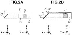
- the detailed configuration of the dichroic mirror 7 is as illustrated in Figs. 2A and 2B .
- the dichroic mirror 7 illustrated in Fig. 1 has the configuration of Fig. 2A . More specifically, the dichroic mirror 7 has a configuration in which transmission surfaces 72 transmitting any light regardless of its wavelength are provided at the right and left in the y axis direction of the dichroic surface 71, which is a light guide surface that reflects the blue color light from the light source 1 and allows the fluorescent light including the green color light and the red color light to transmit there through.
- the dichroic mirror 7 is not limited to the configuration as illustrated in Fig. 2A .
- the dichroic mirror 7 may have such a configuration that the transmission surface 72 is provided around the dichroic surface 71.
- at least one side of the dichroic surface 71 may be configured to overlap a certain side of the transmission surface 72, and the transmission surface 72 may be either a surface on the transparent substrate, or an anti-reflection coated surface.
- a width D d (described below) just needs to be defined in a surface on which the dichroic surface 71 is projected vertically in this cross section.
- the split light fluxes reflected by the dichroic mirror 7 are condensed and overlapped on the fluorescent body 9 by the condenser lens unit 8 having a positive power. As a result, a light source spot is formed on the fluorescent body 9.
- the light source spot formed on the fluorescent body 9 is conjugate to each lens cell (lens surface) of the first lens surface array 61, so that the light source spot has a rectangular uniform distribution.
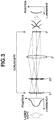
- Fig. 3 is a diagram illustrating, in a simplified manner, an optical relationship of the first lens surface array 61, the second lens surface array 62, the condenser lens unit 8, and the fluorescent body 9 as illustrated in Fig. 1 .
- the first lens surface array 61 corresponds to a first lens surface array 61'
- the second lens surface array 62 corresponds to a second lens surface array 62'
- the condenser lens unit 8 corresponds to a condenser lens unit 8'
- the fluorescent body 9 corresponds to a fluorescent body 9'.
- the fluorescent body 9' is positioned so as to become substantially conjugate to each lens cell of the first lens surface array 61' with the second lens surface array 62' and the condenser lens unit 8'.
- the first lens surface array 61' and the surface of the fluorescent body 9' are in an image-forming relationship. Accordingly, a light source image corresponding to a light distribution formed on each lens cell of the first lens surface array 61' is formed on the fluorescent body 9'.
- the size of the light source image is determined based on a pitch of a lens cell (a width of a lens cell) and a magnification of an image forming system. Furthermore, the light source image formed on each lens cell is disposed to overlap with each other on the fluorescent body 9' via the condenser lens unit 8'.
- the light fluxes made into parallel light by the concave lens 5 are incident upon the first lens surface array 61, they make a discrete light distribution in which the light fluxes from the light sources 1 are separated from each other with an interval.
- a light source image having a uniform light distribution in a shape similar to each lens cell shape of the first lens surface array 61 is formed on the fluorescent body 9. In this manner, the light fluxes from the light sources 1 are less likely to be concentrated on a single spot on the fluorescent body 9, and a reduction in the light emission efficiency due to luminance saturation phenomenon can be suppressed.
- the blue color light emitted from the light source 1 and incident upon the fluorescent body 9 is converted into a fluorescent light mainly including a spectrum of red color light and green color light (conversion light).
- the fluorescent body 9 is formed by applying a fluorescent body layer onto an aluminum substrate having a high reflectance, and the aluminum substrate reflects a fluorescent light subjected to fluorescence conversion from the blue color light toward the condenser lens unit 8.
- the aluminum substrate reflects a part of the blue color light with the same wavelength without being fluorescence-converted.
- the white color light flux including the fluorescent light including red color light and green color light and the unconverted blue color light is emitted from the fluorescent body 9, and condensed and made into parallel light by the condenser lens unit 8.
- the resultant light travels to an illumination optical system (not illustrated).
- the width of the dichroic mirror 7, more specifically the width of the dichroic surface 71 is sufficiently larger than the light flux diameter of the white color light flux from the condenser lens unit 8.
- the blue color light in the white color light flux passing through the dichroic surface 71 is reflected by the dichroic surface 71 and returns to the side of the light source 1. The blue color light thus cannot propagate to the illumination optical system.
- the width of the dichroic surface 71 becomes larger, attenuation of the blue color light increases.
- a configuration having a blue color light source provided separately from the light source 1 emitting excitation light may be considered as discussed in United States Patent Application Publication No. 2012/0133904 , but this configuration increases the size of the entire apparatus. Accordingly, to minimize the attenuated blue color light, minimizing the area of the dichroic mirror 7 is considered in the present exemplary embodiment.
- the width D d of the dichroic surface 71 and the width D c of the condenser lens unit 8 are configured to satisfy the following condition. Namely, the width D d of the dichroic surface 71 is narrower than the width D c of the condenser lens unit 8 in a direction perpendicular to the optical axis of the condenser lens unit 8 (Z axis direction) in a cross section parallel to the normal of the dichroic mirror 7 and including the optical axis of the condenser lens unit 8 (XZ cross section).
- the blue color light which is in the white color light flux from the condenser lens unit 8 and which is included in the light flux passing through the dichroic surface 71 returns to the side of the light source 1, but the light flux not passing through the dichroic mirror 7 is guided to the illumination optical system without change.
- the white color light flux can be guided to the illumination optical system, so that a smaller light source optical system can be realized.
- the width of the dichroic mirror 7 in the Z axis direction may be defined as D d .
- the width of the dichroic surface 71 in the Z axis direction may be defined as D d .
- the width Dd being narrower than the width Dc can be paraphrased as follows: a light flux diameter D LD of the excitation light emitted from the micro lens array 63 is made smaller than the light flux diameter D phos of the white color light flux from the condenser lens unit 8 by using the light flux diameter.
- the definition of the light flux diameter referred to herein will be described with reference to Figs. 4A and 4B .
- Fig. 4A illustrates a luminance cross section diagram of a light source image of excitation light formed on the second lens surface array 62.
- the light fluxes split on the first lens surface array 61 are condensed on the second lens surface array 62, and an image of a light emission point of an LD is formed at the condensing point.
- the luminance cross section diagram illustrated in Fig. 4A has a discrete distribution in which luminance peaks as many as the number corresponding to the lens cell pitch of the first lens surface array 61 are arranged.
- the light flux diameter D LD of the excitation light from the micro lens array 63 is a half width at half maximum of an envelope E of the luminance cross section, i.e., a width where a luminance of 1/2 of the maximum luminance I is obtained.
- Fig. 4B illustrates a luminance cross section diagram of a light distribution of a white color light flux from the condenser lens unit 8. While the fluorescent light from the fluorescent body 9 is emitted in all directions, the surface of the fluorescent body 9 performs surface-emission, and therefore, this can also be understood as a perfect diffusion surface light source. Accordingly, in the luminance cross section of the fluorescence light flux, the luminance is the highest near the optical axis, and the luminance decreases with an increase in distance from the optical axis according to the cosine of the acceptance angle of the fluorescent light by the condenser lens unit 8, but the luminance becomes zero at the limiting point of the acceptance angle that is determined by the effective diameter of the condenser lens. In this case, the light flux diameter of the fluorescent light, i.e., the light flux diameter D phos of the white color light flux from the condenser lens unit 8, corresponds to a width at the position where the luminance is zero.
- the reduction in the size of the light source apparatus can be achieved while the reduction in the light conversion efficiency of the fluorescent body is suppressed.
- Figs. 5A and 5B illustrate the first and second lens surface arrays 61, 62 according to the present exemplary embodiment in an enlarged scale.
- the parallel light fluxes split by the first lens surface array 61 each are condensed on the corresponding lens cell of the second lens surface array 62 by each lens cell of the first lens surface array 61.
- the light source image of the light source 1 is formed on each lens cell of the second lens surface array 62.
- the size of the light source image is larger than the pitch of the lens cell, a part of the light flux may be incident upon a lens cell adjacent to the corresponding lens cell.
- a component forms an image at a position adjacent to a position of a predetermined light source spot on the fluorescent body 9, and such a component is rejected by an optical element in an illumination optical system disposed at a latter stage, resulting in a light that is not effectively used, i.e., a loss. As a result, the light use efficiency is reduced.
- Fig. 5B illustrates a case where the light flux diameter of the excitation light is reduced to reduce the area of the dichroic mirror 7 described above.
- the light source image formed on each lens cell of the second lens surface array 62 is larger than the size of the lens cell, so that a light flux is incident upon a lens cell adjacent to the corresponding lens cell described above, which further reduces the light use efficiency. This is because the angle variation as the parallel light flux of the excitation light flux increases with reduction of the light flux diameter of the excitation light incident upon the first lens surface array 61.
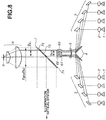
- Fig. 6 is a diagram illustrating a simplified optical relationship among optical elements from the light source 1 to the concave lens 5.
- a light source 1' corresponds to the light source 1.
- Mirrors 2' and 3' are elements having positive powers and each correspond to a mirror of the collimator lens 2 and the parabola mirror array 3, respectively.
- a concave lens 5' is an element having a negative power, and is the concave lens 5 as illustrated.
- the parabola mirror array 3 and the concave lens 5 share the focal point, and form a focal system. Accordingly, the elements 3' and 5' corresponding thereto also form a focal system A.
- the light emitted from the light source 1' is made into parallel light by the collimator lens 2' to be incident upon the focal system A, and the light flux is compressed at a predetermined magnification.
- the light emission point of the light source 1' is infinitely small, the light emitted from the light source 1' is completely made into parallel light by the collimator lens 2', but the light emission point of the LD has a finite size, and accordingly, it is made into a parallel light flux having an angle variation ⁇ 1 corresponding to the size thereof.
- the parallel light flux incident upon the focal system A has an angle variation ⁇ 1 corresponding to the finite size of the light emission point, but when the parallel light is incident upon the aocal system A and the light flux diameter changes, the angle variation changes to ⁇ 2 .
- D 1 and D 2 be the diameters of the parallel light fluxes before and after being incident upon the focal system A, the following formula holds from the relationship of an angular magnification.
- ⁇ denotes the angular magnification. Further reducing the light flux diameter of the excitation light incident upon the first lens surface array 61 described above is equivalent to further reducing the light flux diameter D 2 emitted from the focal system A. When the light flux diameter D2 is reduced, the angular magnification ⁇ increases, and accordingly, the numerical value of the left term increases, and as a result, ⁇ 2 increases.
- the angle variation ⁇ 2 increases, and in the latter stage thereof, the angle variation ⁇ 2 of the parallel light flux incident upon the first lens surface array 61 also increases. Then, as illustrated in Fig. 5B , the size of the light source image on the second lens surface array 62 increases. More specifically, in a case where the light flux diameter of the excitation light is reduced excessively by reducing the area of the dichroic mirror 7 for the purpose of suppressing the attenuation of the blue color light, the size of the light source image formed on the second lens surface array 62 becomes larger than the pitch of the lens cell, and the light use efficiency decreases, which is not desirable.
- a reduction in the size of the light source spot formed on the fluorescent body 9 will be considered.
- the pitch of the lens cell of the second lens surface array 62 is also reduced according to the reduction in the pitch of the lens cell of the first lens surface array 61, the size of the light source image relatively increases with respect to the size of the lens cell. As a result, the light use efficiency decreases, which is not desirable as in the aforementioned case.
- the light flux diameter of the excitation light path and the size of the light source spot on the fluorescent body 9 satisfy the following condition.
- a value obtained by dividing the focal length f c of the condenser lens unit 8 by the light flux diameter is adopted as an F number, and the F number is substituted for the light flux diameter. The reason for this is as follows.
- the focal length is increased in proportion thereto, and the light flux diameter of the fluorescent light may be increased while the acceptance angle is maintained.
- the light flux diameter of the excitation light also changes in proportion to the focal length of the condenser lens, but the light flux diameter can be generalized by dividing each light flux diameter by the focal length of the condenser lens, which is desirable in terms of calculation.
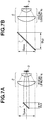
- the F number of the excitation light path i.e., a light path in which the excitation light is condensed on the fluorescent body 9 is larger than the F number of the fluorescent light path, i.e., a light path in which the fluorescent light is condensed by the condenser lens unit 8 as illustrated in Fig. 7A .
- the light source optical system can satisfy the following expression. 0.4 ⁇ F phos F LD ⁇ 0.6
- the F number F LD of the excitation light path increases.
- the light flux diameter D LD of the excitation light is reduced.
- the F number F phos of the fluorescent light path and the F number F LD of the excitation light path are closer to each other.
- the loss increases as illustrated in Fig. 7B , which is not desirable.
- eight LDs are made into a unit, and totally four units are used, i.e., totally 32 LDs are used as a light source, and the light source spot formed on the fluorescent body 9 is in a substantially square shape, one side of which is about 1.0 to 1.5 mm. This is because when the light density of the light source spot on the fluorescent body 9 as described above increases, the light conversion efficiency is reduced due to the luminance saturation phenomenon, or the fluorescent body 9 is degraded in a shorter period of time.
- the size of the light source image formed on the lens cell does not change, and the external shape of the corresponding lens cell becomes relatively smaller.
- the reduction in the light use efficiency occurs as described above, which is not desirable.
- the light source optical system satisfies the following conditional expression. 1.0 ⁇ 1 F LD ⁇ d phos 2 mm 2
- conditional expression (5) means that in a case where the F number F LD of the excitation light path is 1.0 as in the case of the present exemplary embodiment, it is desirable that the area of the light source spot is larger than 1.0 mm 2 . This is because problems occur, e.g., a reduction in the light conversion efficiency due to the increase in the light density of the light source spot on the fluorescent body 9 as described above.
- conditional expression (5) means that in a case where the area of the light source spot is larger than 1.0 mm 2 , the F number F LD of the excitation light path increases, i.e., the light flux diameter D LD of the excitation light is reduced. With this configuration, the area of the dichroic mirror 7 is reduced, so that more unconverted light can be guided from the condenser lens unit 8 to the illumination optical system.
- the lower limit value is less than that of the conditional expression (5).
- the size of the light source image formed on the second lens surface array 62 becomes larger than the pitch of the lens cell as described above, and accordingly, the light use efficiency decreases, which is not desirable.
- the light source optical system can satisfy the following conditional expression. 1.0 ⁇ 1 F LD ⁇ d phos 2 ⁇ 4.0 mm 2
- the cross section area S LD of the excitation light flux can be transformed as in the expression (8) by using the total number of cells N of the lens cell and the area S LA of the lens cell.
- S LD S LA f LA 2 ⁇ N ⁇ S LA ⁇ S LA f LA 2
- conditional expression (5) can be simplified only into the parameter of the lens cell as in the following conditional expression (9).
- the conditional expression (5) or (9) is satisfied, so that the size of the light source spot and the F number F LD of the excitation light, i.e., the light flux diameter D LD of the excitation light, are set to an appropriate relationship.
- the term of SLD in the expressions (7) and (8) can be reduced to 1/4, and therefore, the lower limit value of the conditional expression (9) can be alleviated as follows. 0.25 ⁇ N ⁇ S LA ⁇ S LA f LA 2 mm 2
- the upper limit value of the conditional expression (10) may be set to 4.0.
- Numerical Examples according to the present invention are as follows. [Table 1] Numeric al Example s f c [mm ] D LD [mm ] F LD D pho s [mm ] F ph OS F phos / F LD d pho s [mm ] N S LA [mm 2 ] f LA [mm ] Calculat ion results in conditio nal expressi on (10) [ mm 2 ] 1 15. 0 15. 0 1. 0 30. 0 0. 5 0.5 1.1 961 0.2 3 6.5 1.21 2 15. 0 15. 0 1. 0 30. 0 0. 5 0.5 1.5 529 0.4 2 6.5 2.24 3 15. 0 15. 0 1. 0 30. 0 0.
- Fig. 8 is a diagram illustrating a configuration of a light source apparatus according to the present exemplary embodiment.
- the difference between the first exemplary embodiment described above and the present exemplary embodiment lies in the configuration of the dichroic mirror 7 and the position relationship of the condenser lens unit 8 and the fluorescent body 9 with respect to the dichroic mirror 7.
- the dichroic mirror 7 is configured to include the dichroic surface 71 having characteristics that reflects the excitation light from the light source 1 and allows the fluorescent light from the fluorescent body 9 to transmit there through and the transmission surface 72 allowing the light to transmit there through regardless of the wavelength.
- a dichroic mirror 7 is configured to include a dichroic surface 73 having characteristics that allows excitation light from a light source 1 to transmit there through and reflects fluorescent light from a fluorescent body 9 and a reflection surface 74 reflecting light regardless of the wavelength.
- the dichroic mirror 7 having such a configuration is used, the dichroic mirror 7, a condenser lens unit 8, and the fluorescent body 9 need to be arranged in the direction in which the light flux from the light source 1 travels.
- the white color light flux can be guided to the illumination optical system even if a blue color light source is not provided separately from the light source for excitation light, and a small light source optical system can be realized. Furthermore, the reduction in the light conversion efficiency of the fluorescent body 9 can be suppressed by the micro lens array 63.
- FIG. 9 is a diagram illustrating a configuration of a projector (projection display apparatus) having the light source optical system and the light source apparatus according to the first exemplary embodiment.
- Fig. 9 illustrates a light source apparatus 100 according to the first exemplary embodiment.
- the light source apparatus according to the second exemplary embodiment may be used as the light source apparatus 100 in Fig. 9 .
- An illumination optical system 200 illuminates a liquid crystal panel 20 (optical modulation element) described below by using a light flux from the light source apparatus 100.
- the illumination optical system 200 includes a third fly-eye lens 13a, a fourth fly-eye lens 13b, a polarization conversion element 14, and a condenser lens 15.
- the light flux from the light source apparatus 100 is split into a plurality of light fluxes by the third fly-eye lens 13a, and forms a light source image between the fourth fly-eye lens 13b and the polarization conversion element 14.
- the polarization conversion element 14 is configured to align the polarization direction of the incident light flux in a predetermined direction, and the light flux from the polarization conversion element 14 is guided by the condenser lens 15 to a color separating/combining unit 300.
- the color separating/combining unit 300 includes a polarization plate 16, a dichroic mirror 17, a wavelength selectivity phase difference plate 18, a red color liquid crystal panel 20r, a green color liquid crystal panel 20g, and a blue color liquid crystal panel 20b.
- the liquid crystal panels 20r, 20g, 20b are collectively referred to as a liquid crystal panel 20.
- the color separating/combining unit 300 includes a red color ⁇ /4 plate 19r, a green color ⁇ /4 plate 19g, a blue color ⁇ /4 plate 19b, a first polarization beam splitter 21a, a second polarization beam splitter 21b, and a combining prism 22.
- the red color ⁇ /4 plate 19r, the green color ⁇ /4 plate 19g, and the blue color ⁇ /4 plate 19b are collectively referred to as a ⁇ /4 plate 19.
- a portion of the color separating/combining unit 300 except for the liquid crystal panel 20 is referred to as a color separating and combining system.
- the polarization plate 16 is a polarization plate that allows only the light in the polarization direction aligned by the polarization conversion element 14 to transmit there through, and the blue color light and the red color light in the light from the polarization plate 16 is guided by the dichroic mirror 17 toward the second polarization beam splitter 21b. The green color light is guided toward the first polarization beam splitter 21a.
- the first polarization beam splitter 21a and the second polarization beam splitter 21b are configured to guide the light from the dichroic mirror 17 to the liquid crystal panel 20 according to the polarization direction, and guide the light from the liquid crystal panel 20 to the combining prism 22.
- the ⁇ /4 plate 19 gives a phase difference of ⁇ /2 in the reciprocation made by the reflection at the liquid crystal panel 20, so that the ⁇ /4 plate 19 has an effect of enhancing the analysis effect.
- the combining prism 22 combines the blue color light and the red color light from the second polarization beam splitter 21b and the green color light from the first polarization beam splitter 21a, and guides the combined light to a projection optical system 23.
- the projector illustrated in Fig. 8 can project a color image onto a projection surface such as a screen.
- a positional relationship of the light source apparatus 100, the illumination optical system 200, the color separating/combining unit 300, and the projection optical system 23 with one another may not be a relationship as illustrated in Fig. 8 .
- all of the optical axis of the condenser lens unit 8, the optical axis of the condenser lens 15, a surface normal of the liquid crystal panel 20, and the optical axis of the projection optical system 23 exist in the same plane in Fig. 8 .
- each axis does not necessarily exist in the same plane, and may be changed as necessary so that the surface where they exist may be different depending on the axis by using a mirror and the like.
- Each exemplary embodiment described above shows an example of a configuration in which the surface of the micro lens array 63 facing the concave lens 5 is the first lens surface array 61, and a surface of the micro lens array 63 facing the side of the dichroic mirror 7 is the second lens surface array 62.
- Such a configuration can be used to suppress a relative displacement between both the micro lens array 63 and the first lens surface array 61.
- a first fly-eye lens having the first lens surface array 61 and a second fly-eye lens having the second lens surface array 62 may be provided in that order from the side of the concave lens 5. In this case, the volume during glass formation can be reduced, so that it takes less time to form the glass.
- the light source 1 and the collimator lens 2 may be held by separate holding members, or may be held by the same holding member.
- an LD bank integrally including eight light sources 1 and eight collimator lenses 2 may be used.
- the light flux from the parabola mirror array 3 may be guided to the concave lens 5 by using a prism instead of the flat mirror 4 according to each of the above embodiments.
- a light source image is formed on the second lens surface array 62 by the first lens surface array 61.
- the light source image should only be formed near the second lens surface array 62.
- the light source image may be formed between the second lens surface array 62 and the fluorescent body 9, or between the second lens surface array 62 and the dichroic mirror 7.
- the configuration of the fluorescent body 9 made by applying a fluorescent body layer onto a high reflectance aluminum substrate has been illustrated as an example. More specifically, this may be a configuration in which a wheel made by continuously applying a fluorescent body layer in a peripheral direction on a circular aluminum substrate may be rotated with a motor. According to such a configuration, the position where the laser light from the light source 1 is condensed on the fluorescent body layer is changed, so that the degradation of the fluorescent body layer can be suppressed.
- the dichroic surface 71 is provided as the light guide surface, but the present invention is not limited to such a configuration.
- the light fluxes from multiple light sources 1 may be aligned in the predetermined polarization direction, and instead of the dichroic surface 71, a polarization dividing surface may be provided as the light guide surface.
- the light fluxes from the fluorescent body 9 are emitted in such a state that the polarization directions are not organized, and accordingly, on the polarization dividing surface, a light flux having the same wavelength as the light flux from the light source 1 can also be guided to the illumination optical system.
Landscapes
- Physics & Mathematics (AREA)
- General Physics & Mathematics (AREA)
- Optics & Photonics (AREA)
- Engineering & Computer Science (AREA)
- Multimedia (AREA)
- Projection Apparatus (AREA)
- Non-Portable Lighting Devices Or Systems Thereof (AREA)
Applications Claiming Priority (1)
| Application Number | Priority Date | Filing Date | Title |
|---|---|---|---|
| JP2015232534A JP6525856B2 (ja) | 2015-11-28 | 2015-11-28 | 光源光学系およびこれを用いた投射型表示装置 |
Publications (1)
| Publication Number | Publication Date |
|---|---|
| EP3173849A1 true EP3173849A1 (en) | 2017-05-31 |
Family
ID=57391830
Family Applications (1)
| Application Number | Title | Priority Date | Filing Date |
|---|---|---|---|
| EP16199961.0A Withdrawn EP3173849A1 (en) | 2015-11-28 | 2016-11-22 | Light source optical system and projection display apparatus employing the same |
Country Status (4)
| Country | Link |
|---|---|
| US (2) | US9921462B2 (ja) |
| EP (1) | EP3173849A1 (ja) |
| JP (1) | JP6525856B2 (ja) |
| CN (2) | CN106842789B (ja) |
Families Citing this family (18)
| Publication number | Priority date | Publication date | Assignee | Title |
|---|---|---|---|---|
| JP6525856B2 (ja) * | 2015-11-28 | 2019-06-05 | キヤノン株式会社 | 光源光学系およびこれを用いた投射型表示装置 |
| CN108761981B (zh) * | 2018-04-28 | 2020-10-20 | 苏州佳世达光电有限公司 | 投影机 |
| JP7341740B2 (ja) * | 2019-06-12 | 2023-09-11 | キヤノン株式会社 | 光源装置および画像投射装置 |
| CN112213908B (zh) * | 2019-07-12 | 2022-12-02 | 深圳光峰科技股份有限公司 | 光源系统与显示设备 |
| CN110715192A (zh) * | 2019-11-27 | 2020-01-21 | 广州市超亮电子科技有限公司 | 蓝色激光转化为白光点光源的装置 |
| JP7400417B2 (ja) * | 2019-11-29 | 2023-12-19 | 株式会社リコー | 光源光学系、光源装置及び画像表示装置 |
| JP2021128273A (ja) * | 2020-02-14 | 2021-09-02 | キヤノン株式会社 | 光源装置、およびこれを備える画像投写装置 |
| CN212112106U (zh) * | 2020-04-20 | 2020-12-08 | 深圳光峰科技股份有限公司 | 一种光引导元件以及光源装置 |
| JP7484448B2 (ja) | 2020-06-04 | 2024-05-16 | セイコーエプソン株式会社 | 照明装置およびプロジェクター |
| JP7400632B2 (ja) | 2020-06-04 | 2023-12-19 | セイコーエプソン株式会社 | 照明装置およびプロジェクター |
| CN113946090A (zh) * | 2020-07-15 | 2022-01-18 | 深圳光峰科技股份有限公司 | 一种光源系统与投影系统 |
| JP7428095B2 (ja) | 2020-07-21 | 2024-02-06 | セイコーエプソン株式会社 | 照明装置およびプロジェクター |
| JP2022021957A (ja) | 2020-07-23 | 2022-02-03 | セイコーエプソン株式会社 | 照明装置およびプロジェクター |
| CN114063375B (zh) * | 2020-08-10 | 2024-01-23 | 成都极米科技股份有限公司 | 一种光源系统 |
| CN114114812B (zh) | 2020-08-27 | 2023-04-21 | 精工爱普生株式会社 | 照明装置和投影仪 |
| JP2022144381A (ja) | 2021-03-19 | 2022-10-03 | セイコーエプソン株式会社 | 照明装置およびプロジェクター |
| JP7405123B2 (ja) | 2021-09-28 | 2023-12-26 | セイコーエプソン株式会社 | 光源装置、照明装置およびプロジェクター |
| CN114815276A (zh) * | 2022-05-03 | 2022-07-29 | 安徽师范大学 | 一种采用复眼透镜的均匀照明光学系统 |
Citations (9)
| Publication number | Priority date | Publication date | Assignee | Title |
|---|---|---|---|---|
| US20110234998A1 (en) * | 2010-03-24 | 2011-09-29 | Casio Computer Co., Ltd. | Light source unit and projector |
| US20120133904A1 (en) | 2010-11-29 | 2012-05-31 | Seiko Epson Corporation | Light source device and projector |
| US20130250253A1 (en) * | 2012-03-21 | 2013-09-26 | Casio Computer Co., Ltd. | Light source device and projector |
| EP2650593A1 (en) * | 2010-12-08 | 2013-10-16 | Appotronics (China) Corporation | Light source |
| US20130322056A1 (en) * | 2012-05-30 | 2013-12-05 | Hitachi Media Eletronics Co., Ltd. | Light source device and image display apparatus |
| US20140022512A1 (en) * | 2012-07-19 | 2014-01-23 | Wavien, Inc. | Phosphor-based lamps for projection display |
| EP2757414A2 (en) * | 2013-01-17 | 2014-07-23 | Delta Electronics, Inc. | Optical light source system for a projector |
| US20150222864A1 (en) * | 2014-02-03 | 2015-08-06 | Canon Kabushiki Kaisha | Light source optical system, light source apparatus using the same, and image display apparatus |
| DE102014202090A1 (de) * | 2014-02-05 | 2015-08-06 | Osram Gmbh | Beleuchtungsvorrichtung mit einer Wellenlängenkonversionsanordnung |
Family Cites Families (17)
| Publication number | Priority date | Publication date | Assignee | Title |
|---|---|---|---|---|
| US7054067B2 (en) * | 2003-05-27 | 2006-05-30 | Nippon Hoso Kyokai | Three-dimensional image optical system |
| US20070177263A1 (en) * | 2004-07-23 | 2007-08-02 | Kuraray Co. Ltd | Back projection-type screen and back projection-type projection device |
| CN202109406U (zh) * | 2010-12-08 | 2012-01-11 | 绎立锐光科技开发(深圳)有限公司 | 光波长转换轮组件及带该光波长转换轮组件的光源 |
| JP5675320B2 (ja) * | 2010-12-17 | 2015-02-25 | 日立マクセル株式会社 | 光源装置、および、投写型映像表示装置 |
| JP5648556B2 (ja) * | 2011-03-28 | 2015-01-07 | ソニー株式会社 | 照明装置、投射型表示装置および直視型表示装置 |
| JP5849613B2 (ja) * | 2011-10-31 | 2016-01-27 | 株式会社リコー | 画像表示装置 |
| JP5915124B2 (ja) * | 2011-11-30 | 2016-05-11 | セイコーエプソン株式会社 | 光源装置及びプロジェクター |
| JP2014119471A (ja) | 2012-12-13 | 2014-06-30 | Seiko Epson Corp | 光源装置及びプロジェクター |
| JP5766371B2 (ja) * | 2013-01-23 | 2015-08-19 | 三菱電機株式会社 | 投写装置 |
| JP2014182358A (ja) * | 2013-03-21 | 2014-09-29 | Hitachi Media Electoronics Co Ltd | 光源装置及び画像表示装置 |
| JP6205784B2 (ja) * | 2013-03-28 | 2017-10-04 | セイコーエプソン株式会社 | 照明装置及びプロジェクター |
| JP6335532B2 (ja) * | 2014-02-03 | 2018-05-30 | キヤノン株式会社 | 照明光学系、画像投射装置およびその制御方法 |
| JP6375626B2 (ja) | 2014-01-17 | 2018-08-22 | セイコーエプソン株式会社 | 光源装置およびプロジェクター |
| JP2015145976A (ja) * | 2014-02-03 | 2015-08-13 | キヤノン株式会社 | 光源装置およびこれを用いた投射型表示装置 |
| JP2015145975A (ja) * | 2014-02-03 | 2015-08-13 | キヤノン株式会社 | 光源装置およびこれを用いた投射型表示装置 |
| JP6536202B2 (ja) * | 2015-06-18 | 2019-07-03 | セイコーエプソン株式会社 | 光源装置、照明装置およびプロジェクター |
| JP6525856B2 (ja) * | 2015-11-28 | 2019-06-05 | キヤノン株式会社 | 光源光学系およびこれを用いた投射型表示装置 |
-
2015
- 2015-11-28 JP JP2015232534A patent/JP6525856B2/ja active Active
-
2016
- 2016-11-18 CN CN201611024637.XA patent/CN106842789B/zh active Active
- 2016-11-18 CN CN201811619864.6A patent/CN109541879B/zh active Active
- 2016-11-18 US US15/356,265 patent/US9921462B2/en active Active
- 2016-11-22 EP EP16199961.0A patent/EP3173849A1/en not_active Withdrawn
-
2018
- 2018-01-29 US US15/882,349 patent/US10133169B2/en active Active
Patent Citations (9)
| Publication number | Priority date | Publication date | Assignee | Title |
|---|---|---|---|---|
| US20110234998A1 (en) * | 2010-03-24 | 2011-09-29 | Casio Computer Co., Ltd. | Light source unit and projector |
| US20120133904A1 (en) | 2010-11-29 | 2012-05-31 | Seiko Epson Corporation | Light source device and projector |
| EP2650593A1 (en) * | 2010-12-08 | 2013-10-16 | Appotronics (China) Corporation | Light source |
| US20130250253A1 (en) * | 2012-03-21 | 2013-09-26 | Casio Computer Co., Ltd. | Light source device and projector |
| US20130322056A1 (en) * | 2012-05-30 | 2013-12-05 | Hitachi Media Eletronics Co., Ltd. | Light source device and image display apparatus |
| US20140022512A1 (en) * | 2012-07-19 | 2014-01-23 | Wavien, Inc. | Phosphor-based lamps for projection display |
| EP2757414A2 (en) * | 2013-01-17 | 2014-07-23 | Delta Electronics, Inc. | Optical light source system for a projector |
| US20150222864A1 (en) * | 2014-02-03 | 2015-08-06 | Canon Kabushiki Kaisha | Light source optical system, light source apparatus using the same, and image display apparatus |
| DE102014202090A1 (de) * | 2014-02-05 | 2015-08-06 | Osram Gmbh | Beleuchtungsvorrichtung mit einer Wellenlängenkonversionsanordnung |
Also Published As
| Publication number | Publication date |
|---|---|
| CN106842789A (zh) | 2017-06-13 |
| JP2017097310A (ja) | 2017-06-01 |
| US10133169B2 (en) | 2018-11-20 |
| US9921462B2 (en) | 2018-03-20 |
| US20180149956A1 (en) | 2018-05-31 |
| CN106842789B (zh) | 2019-01-18 |
| CN109541879A (zh) | 2019-03-29 |
| US20170153538A1 (en) | 2017-06-01 |
| JP6525856B2 (ja) | 2019-06-05 |
| CN109541879B (zh) | 2021-05-04 |
Similar Documents
| Publication | Publication Date | Title |
|---|---|---|
| EP3173849A1 (en) | Light source optical system and projection display apparatus employing the same | |
| US10338461B2 (en) | Light-emitting device and related light source system | |
| US10082731B2 (en) | Illumination apparatus and projection display apparatus using the same | |
| US10175566B2 (en) | Light source device, illumination device, and projector | |
| GB2531920A (en) | Optical unit, optical apparatus using the same, light source apparatus, and projection display apparatus | |
| EP3792690A1 (en) | Light source system, projection device and illumination device | |
| US11223806B2 (en) | Light source system, method for improving light efficiency thereof, and display device | |
| US10634981B2 (en) | Light source device and projection type display apparatus | |
| JP2017215496A (ja) | 光源光学系およびこれを用いた画像表示装置 | |
| US20220382137A1 (en) | Light-source optical system, light-source device, and image display apparatus | |
| JP6790170B2 (ja) | 光源光学系およびこれを用いた投射型表示装置 | |
| US9851631B2 (en) | Light source optical system and projection display apparatus employing the same | |
| JP7086518B2 (ja) | 光源光学系およびこれを用いた投射型表示装置 | |
| WO2021143438A1 (zh) | 波长转换装置、光源装置及投影系统 | |
| EP3961288A1 (en) | Optical system | |
| US20210352250A1 (en) | Display apparatus and display system | |
| JP6711705B2 (ja) | 照明装置およびこれを用いた投射型表示装置 | |
| US11874592B2 (en) | Light source device and image projection apparatus | |
| CN219105335U (zh) | 发光装置 | |
| CN215494522U (zh) | 一种缩束元件、光源装置及投影系统 | |
| CN114397793A (zh) | 一种混合光源装置及投影系统 | |
| CN115236926A (zh) | 一种激光荧光光源 |
Legal Events
| Date | Code | Title | Description |
|---|---|---|---|
| PUAI | Public reference made under article 153(3) epc to a published international application that has entered the european phase |
Free format text: ORIGINAL CODE: 0009012 |
|
| STAA | Information on the status of an ep patent application or granted ep patent |
Free format text: STATUS: THE APPLICATION HAS BEEN PUBLISHED |
|
| AK | Designated contracting states |
Kind code of ref document: A1 Designated state(s): AL AT BE BG CH CY CZ DE DK EE ES FI FR GB GR HR HU IE IS IT LI LT LU LV MC MK MT NL NO PL PT RO RS SE SI SK SM TR |
|
| AX | Request for extension of the european patent |
Extension state: BA ME |
|
| STAA | Information on the status of an ep patent application or granted ep patent |
Free format text: STATUS: REQUEST FOR EXAMINATION WAS MADE |
|
| 17P | Request for examination filed |
Effective date: 20171130 |
|
| RBV | Designated contracting states (corrected) |
Designated state(s): AL AT BE BG CH CY CZ DE DK EE ES FI FR GB GR HR HU IE IS IT LI LT LU LV MC MK MT NL NO PL PT RO RS SE SI SK SM TR |
|
| STAA | Information on the status of an ep patent application or granted ep patent |
Free format text: STATUS: EXAMINATION IS IN PROGRESS |
|
| STAA | Information on the status of an ep patent application or granted ep patent |
Free format text: STATUS: EXAMINATION IS IN PROGRESS |
|
| 17Q | First examination report despatched |
Effective date: 20210924 |
|
| GRAP | Despatch of communication of intention to grant a patent |
Free format text: ORIGINAL CODE: EPIDOSNIGR1 |
|
| STAA | Information on the status of an ep patent application or granted ep patent |
Free format text: STATUS: GRANT OF PATENT IS INTENDED |
|
| INTG | Intention to grant announced |
Effective date: 20230516 |
|
| STAA | Information on the status of an ep patent application or granted ep patent |
Free format text: STATUS: THE APPLICATION HAS BEEN WITHDRAWN |
|
| 18W | Application withdrawn |
Effective date: 20230913 |