EP3141635B1 - Semiconductor substrate, epitaxial wafer, and method for manufacturing epitaxial wafer - Google Patents
Semiconductor substrate, epitaxial wafer, and method for manufacturing epitaxial wafer Download PDFInfo
- Publication number
- EP3141635B1 EP3141635B1 EP15789328.0A EP15789328A EP3141635B1 EP 3141635 B1 EP3141635 B1 EP 3141635B1 EP 15789328 A EP15789328 A EP 15789328A EP 3141635 B1 EP3141635 B1 EP 3141635B1
- Authority
- EP
- European Patent Office
- Prior art keywords
- single crystal
- gas
- plane
- semiconductor substrate
- epitaxial layer
- Prior art date
- Legal status (The legal status is an assumption and is not a legal conclusion. Google has not performed a legal analysis and makes no representation as to the accuracy of the status listed.)
- Active
Links
Images


Classifications
-
- C—CHEMISTRY; METALLURGY
- C30—CRYSTAL GROWTH
- C30B—SINGLE-CRYSTAL GROWTH; UNIDIRECTIONAL SOLIDIFICATION OF EUTECTIC MATERIAL OR UNIDIRECTIONAL DEMIXING OF EUTECTOID MATERIAL; REFINING BY ZONE-MELTING OF MATERIAL; PRODUCTION OF A HOMOGENEOUS POLYCRYSTALLINE MATERIAL WITH DEFINED STRUCTURE; SINGLE CRYSTALS OR HOMOGENEOUS POLYCRYSTALLINE MATERIAL WITH DEFINED STRUCTURE; AFTER-TREATMENT OF SINGLE CRYSTALS OR A HOMOGENEOUS POLYCRYSTALLINE MATERIAL WITH DEFINED STRUCTURE; APPARATUS THEREFOR
- C30B25/00—Single-crystal growth by chemical reaction of reactive gases, e.g. chemical vapour-deposition growth
- C30B25/02—Epitaxial-layer growth
- C30B25/18—Epitaxial-layer growth characterised by the substrate
- C30B25/20—Epitaxial-layer growth characterised by the substrate the substrate being of the same materials as the epitaxial layer
-
- C—CHEMISTRY; METALLURGY
- C23—COATING METALLIC MATERIAL; COATING MATERIAL WITH METALLIC MATERIAL; CHEMICAL SURFACE TREATMENT; DIFFUSION TREATMENT OF METALLIC MATERIAL; COATING BY VACUUM EVAPORATION, BY SPUTTERING, BY ION IMPLANTATION OR BY CHEMICAL VAPOUR DEPOSITION, IN GENERAL; INHIBITING CORROSION OF METALLIC MATERIAL OR INCRUSTATION IN GENERAL
- C23C—COATING METALLIC MATERIAL; COATING MATERIAL WITH METALLIC MATERIAL; SURFACE TREATMENT OF METALLIC MATERIAL BY DIFFUSION INTO THE SURFACE, BY CHEMICAL CONVERSION OR SUBSTITUTION; COATING BY VACUUM EVAPORATION, BY SPUTTERING, BY ION IMPLANTATION OR BY CHEMICAL VAPOUR DEPOSITION, IN GENERAL
- C23C16/00—Chemical coating by decomposition of gaseous compounds, without leaving reaction products of surface material in the coating, i.e. chemical vapour deposition [CVD] processes
- C23C16/44—Chemical coating by decomposition of gaseous compounds, without leaving reaction products of surface material in the coating, i.e. chemical vapour deposition [CVD] processes characterised by the method of coating
-
- C—CHEMISTRY; METALLURGY
- C30—CRYSTAL GROWTH
- C30B—SINGLE-CRYSTAL GROWTH; UNIDIRECTIONAL SOLIDIFICATION OF EUTECTIC MATERIAL OR UNIDIRECTIONAL DEMIXING OF EUTECTOID MATERIAL; REFINING BY ZONE-MELTING OF MATERIAL; PRODUCTION OF A HOMOGENEOUS POLYCRYSTALLINE MATERIAL WITH DEFINED STRUCTURE; SINGLE CRYSTALS OR HOMOGENEOUS POLYCRYSTALLINE MATERIAL WITH DEFINED STRUCTURE; AFTER-TREATMENT OF SINGLE CRYSTALS OR A HOMOGENEOUS POLYCRYSTALLINE MATERIAL WITH DEFINED STRUCTURE; APPARATUS THEREFOR
- C30B29/00—Single crystals or homogeneous polycrystalline material with defined structure characterised by the material or by their shape
- C30B29/10—Inorganic compounds or compositions
- C30B29/16—Oxides
-
- H—ELECTRICITY
- H10—SEMICONDUCTOR DEVICES; ELECTRIC SOLID-STATE DEVICES NOT OTHERWISE PROVIDED FOR
- H10D—INORGANIC ELECTRIC SEMICONDUCTOR DEVICES
- H10D62/00—Semiconductor bodies, or regions thereof, of devices having potential barriers
- H10D62/40—Crystalline structures
- H10D62/405—Orientations of crystalline planes
-
- H—ELECTRICITY
- H10—SEMICONDUCTOR DEVICES; ELECTRIC SOLID-STATE DEVICES NOT OTHERWISE PROVIDED FOR
- H10D—INORGANIC ELECTRIC SEMICONDUCTOR DEVICES
- H10D62/00—Semiconductor bodies, or regions thereof, of devices having potential barriers
- H10D62/80—Semiconductor bodies, or regions thereof, of devices having potential barriers characterised by the materials
- H10D62/875—Semiconductor bodies, or regions thereof, of devices having potential barriers characterised by the materials being semiconductor metal oxide, e.g. InGaZnO
-
- H—ELECTRICITY
- H10—SEMICONDUCTOR DEVICES; ELECTRIC SOLID-STATE DEVICES NOT OTHERWISE PROVIDED FOR
- H10P—GENERIC PROCESSES OR APPARATUS FOR THE MANUFACTURE OR TREATMENT OF DEVICES COVERED BY CLASS H10
- H10P14/00—Formation of materials, e.g. in the shape of layers or pillars
- H10P14/20—Formation of materials, e.g. in the shape of layers or pillars of semiconductor materials
- H10P14/24—Formation of materials, e.g. in the shape of layers or pillars of semiconductor materials using chemical vapour deposition [CVD]
-
- H—ELECTRICITY
- H10—SEMICONDUCTOR DEVICES; ELECTRIC SOLID-STATE DEVICES NOT OTHERWISE PROVIDED FOR
- H10P—GENERIC PROCESSES OR APPARATUS FOR THE MANUFACTURE OR TREATMENT OF DEVICES COVERED BY CLASS H10
- H10P14/00—Formation of materials, e.g. in the shape of layers or pillars
- H10P14/20—Formation of materials, e.g. in the shape of layers or pillars of semiconductor materials
- H10P14/29—Formation of materials, e.g. in the shape of layers or pillars of semiconductor materials characterised by the substrates
- H10P14/2901—Materials
- H10P14/2918—Materials being semiconductor metal oxides
-
- H—ELECTRICITY
- H10—SEMICONDUCTOR DEVICES; ELECTRIC SOLID-STATE DEVICES NOT OTHERWISE PROVIDED FOR
- H10P—GENERIC PROCESSES OR APPARATUS FOR THE MANUFACTURE OR TREATMENT OF DEVICES COVERED BY CLASS H10
- H10P14/00—Formation of materials, e.g. in the shape of layers or pillars
- H10P14/20—Formation of materials, e.g. in the shape of layers or pillars of semiconductor materials
- H10P14/29—Formation of materials, e.g. in the shape of layers or pillars of semiconductor materials characterised by the substrates
- H10P14/2924—Structures
- H10P14/2925—Surface structures
-
- H—ELECTRICITY
- H10—SEMICONDUCTOR DEVICES; ELECTRIC SOLID-STATE DEVICES NOT OTHERWISE PROVIDED FOR
- H10P—GENERIC PROCESSES OR APPARATUS FOR THE MANUFACTURE OR TREATMENT OF DEVICES COVERED BY CLASS H10
- H10P14/00—Formation of materials, e.g. in the shape of layers or pillars
- H10P14/20—Formation of materials, e.g. in the shape of layers or pillars of semiconductor materials
- H10P14/29—Formation of materials, e.g. in the shape of layers or pillars of semiconductor materials characterised by the substrates
- H10P14/2926—Crystal orientations
-
- H—ELECTRICITY
- H10—SEMICONDUCTOR DEVICES; ELECTRIC SOLID-STATE DEVICES NOT OTHERWISE PROVIDED FOR
- H10P—GENERIC PROCESSES OR APPARATUS FOR THE MANUFACTURE OR TREATMENT OF DEVICES COVERED BY CLASS H10
- H10P14/00—Formation of materials, e.g. in the shape of layers or pillars
- H10P14/20—Formation of materials, e.g. in the shape of layers or pillars of semiconductor materials
- H10P14/34—Deposited materials, e.g. layers
- H10P14/3402—Deposited materials, e.g. layers characterised by the chemical composition
- H10P14/3434—Deposited materials, e.g. layers characterised by the chemical composition being oxide semiconductor materials
-
- H—ELECTRICITY
- H10—SEMICONDUCTOR DEVICES; ELECTRIC SOLID-STATE DEVICES NOT OTHERWISE PROVIDED FOR
- H10P—GENERIC PROCESSES OR APPARATUS FOR THE MANUFACTURE OR TREATMENT OF DEVICES COVERED BY CLASS H10
- H10P14/00—Formation of materials, e.g. in the shape of layers or pillars
- H10P14/20—Formation of materials, e.g. in the shape of layers or pillars of semiconductor materials
- H10P14/34—Deposited materials, e.g. layers
- H10P14/3451—Structure
- H10P14/3452—Microstructure
- H10P14/3458—Monocrystalline
Definitions
- the invention relates to an epitaxial wafer and a method for manufacturing the epitaxial wafer.
- a technique of forming a ⁇ -Ga 2 O 3 single crystal film on a ⁇ -Ga 2 O 3 -based substrate by epitaxial crystal growth using the MBE (Molecular Beam Epitaxy) method is conventionally known (see, e.g., PTL 1).
- the ⁇ -Ga 2 O 3 single crystal film can be grown at a high growth rate by the MBE method when the plane orientation of the principal surface of the P-Ga 2 O 3 -based substrate is adjusted to a predetermined plane orientation.
- NPL 1, PTL 2 and PTL 3 show the homoepitaxial growth of beta-Ga2O3.
- NPL 1 KOHEI SASAKI ET AL: "MBE grown Ga2O3 and its power device applications", JOURNAL OF CRYSTAL GROWTH, vol. 378, 1 September 2013, pages 591-595 .
- an epitaxial wafer defined by claim 1 is provided.
- a semiconductor substrate comprising a ⁇ -Ga 2 O 3 single crystal that allows an epitaxial layer comprising a ⁇ -Ga 2 O 3 single crystal to grow thereon at a high growth rate using the HVPE method, an epitaxial wafer comprising the semiconductor substrate and an epitaxial layer, and a method for manufacturing the epitaxial wafer can be provided.
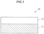
- FIG.1 is a vertical cross-sectional view showing an epitaxial wafer 10 in the first embodiment.
- the epitaxial wafer 10 has a semiconductor substrate 11 and an epitaxial layer 12 formed on a principal surface of the semiconductor substrate 11 by epitaxial crystal growth using the HVPE (Halide Vapor Phase Epitaxy) method.
- HVPE Hydrode Vapor Phase Epitaxy
- the semiconductor substrate 11 is a substrate formed of a ⁇ -Ga 2 O 3 -based single crystal.
- the ⁇ -Ga 2 O 3 -based single crystal here means a ⁇ -Ga 2 O 3 single crystal or a crystal of which base crystal is a ⁇ -Ga 2 O 3 single crystal doped with an element such as Al or In.
- the composition of the ⁇ -Ga 2 O 3 single crystal doped with, e.g., Al and In is expressed by ⁇ -(Ga x Al y In (1-x-y) ) 2 O 3 ( 0 ⁇ x ⁇ 1 , 0 ⁇ y ⁇ 1 , 0 ⁇ x+y ⁇ 1 ).
- the band gap of the ⁇ -Ga 2 O 3 single crystal is widened by adding Al and is narrowed by adding In.
- the semiconductor substrate 11 may also contain a conductive impurity such as Si.
- a bulk crystal of a GazOs-based single crystal grown by, e.g., a melt-growth technique such as the FZ (Floating Zone) method or the EFG (Edge Defined Film Fed Growth) method is sliced and the surface thereof is then polished.
- the principal surface of the semiconductor substrate 11 is a plane parallel to a [ 010 ] axis of the ⁇ -Ga 2 O 3 -based single crystal which constitutes the semiconductor substrate 11 . This is determined based on the finding by the present inventors that a growth rate of a ⁇ -Ga 2 O 3 -based single crystal layer epitaxially grown by the HVPE method is extremely low when the principal surface of the ⁇ -Ga 2 O 3 -based single crystal substrate has a plane orientation of ( 010 ).
- the present inventors found that the growth rate of a ⁇ -Ga 2 O 3 -based single crystal layer epitaxially grown by the HVPE method is high when the plane orientation of the principal surface of the ⁇ -Ga 2 O 3 -based single crystal substrate is perpendicular to a ( 010 ) plane which is not suitable for growing the ⁇ -Ga 2 O 3 -based single crystal layer using the HVPE method, i.e., when the principal surface is a plane parallel to the [ 010 ] axis.
- the principal surface of the semiconductor substrate 11 is a plane rotated by an angle within a range of not less than 38 ° and not more than 90 ° from a ( 100 ) plane toward a ( 101 ) plane about the [ 010 ] axis of the ⁇ -Ga 2 O 3 -based single crystal.
- the principal surface of the semiconductor substrate 11 is a plane rotated by 68 ⁇ 10° from a ( 100 ) plane toward a ( 101 ) plane about the [ 010 ] axis of the ⁇ -Ga 2 O 3 -based single crystal.
- ⁇ here indicates the tolerance and 68 ⁇ 10 °, for example, means a given angle within a range of not less than 58 ° and not more than 78 °.
- the principal surface of the semiconductor substrate 11 is a plane rotated by 38 ⁇ 1 °, 68 ⁇ 1 °, 77.3 ⁇ 1 °, 83 ⁇ 1 ° or 90 ⁇ 1 ° from a ( 100 ) plane toward a ( 101 ) plane about the [ 010 ] axis of the ⁇ -Ga 2 O 3 -based single crystal.
- the rotations of 53.8° and 76.3° are not part of this disclosure.
- the epitaxial layer 12 is formed of a ⁇ -Ga 2 O 3 -based single crystal in the same manner as the semiconductor substrate 11.
- the epitaxial layer 12 may also contain a conductive impurity such as Si.
- a structure of a vapor phase deposition system used for growing the epitaxial layer 12 in the present embodiment will be described below as an example.
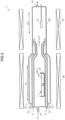
- FIG2 is a vertical cross-sectional view showing a vapor phase deposition system 2 in the embodiment.
- the vapor phase deposition system 2 is a vapor phase deposition system using HVPE technique, and has a reaction chamber 20 having a first gas introducing port 21 , a second gas introducing port 22 , a third gas introducing port 23 and an exhaust port 24 , and a first heating means 26 and a second heating means 27 which are placed around the reaction chamber 20 to heat predetermined regions in the reaction chamber 20 .
- the film growth rate when using the HVPE technique is higher than that in the PLD method, etc.
- in-plane distribution of film thickness is highly uniform and it is possible to grow a large-diameter film. Therefore, it is suitable for mass production of crystal.
- the reaction chamber 20 has a source reaction region R 1 in which a reaction container 25 containing a Ga material is placed and a gallium source gas is produced, and a crystal growth region R 2 in which the semiconductor substrate 11 is placed and the epitaxial layer 12 is grown thereon.
- the reaction chamber 20 is formed of, e.g., quartz glass.
- reaction container 25 is formed of, e.g., quartz glass and the Ga material contained in the reaction container 25 is metal gallium.
- the first heating means 26 and the second heating means 27 are capable of respectively heating the source reaction region R 1 and the crystal growth region R 2 of the reaction chamber 20.
- the first heating means 26 and the second heating means 27 are, e.g., resistive heaters or radiation heaters.
- the first gas introducing port 21 is a port for introducing a Cl-containing gas (Cl 2 gas or HCl gas) into the source reaction region R 1 of the reaction chamber 20 using an inert carrier gas (N 2 gas, Ar gas or He gas).
- a Cl-containing gas Cl 2 gas or HCl gas
- N 2 gas, Ar gas or He gas an inert carrier gas
- the second gas introducing port 22 is a port for introducing an oxygen-containing gas (Oz gas or HzO gas, etc.) as an oxygen source gas and a chloride gas (e.g., silicon tetrachloride, etc.) used to add a dopant such as Si to the epitaxial layer 12 , into the crystal growth region R 2 of the reaction chamber 20 using an inert carrier gas (N 2 gas, Ar gas or He gas).
- an oxygen-containing gas oxygen-containing gas or HzO gas, etc.
- a chloride gas e.g., silicon tetrachloride, etc.
- the third gas introducing port 23 is a port for introducing an inert carrier gas (N 2 gas, Ar gas or He gas) into the crystal growth region R 2 of the reaction chamber 20.
- a process of growing the epitaxial layer 12 in the present embodiment will be described below as an example.
- the source reaction region R 1 of the reaction chamber 20 is heated by the first heating means 26 and an atmosphere temperature in the source reaction region R 1 is then maintained at a predetermined temperature.
- a Cl-containing gas introduced through the first gas introducing port 21 using a carrier gas is reacted with the metal gallium in the reaction container 25 at the above-mentioned atmosphere temperature, thereby producing a gallium chloride gas.
- the atmosphere temperature in the source reaction region R 1 here is preferably a temperature at which GaCl gas has the highest partial pressure among component gases of the gallium chloride gas produced by the reaction of the metal gallium in the reaction container 25 with the Cl-containing gas.
- the gallium chloride gas here contains GaCl gas, GaCl 2 gas, GaCl 3 gas and (GaCl 3 ) 2 gas, etc.
- the temperature at which a driving force for growth of Ga 2 O 3 crystal is maintained is the highest with the GaCl gas among the gases contained in the gallium chloride gas. Growth at a high temperature is effective to obtain a high-quality Ga 2 O 3 crystal with high purity. Therefore, for growing the epitaxial layer 12 , it is preferable to produce a gallium chloride gas in which a partial pressure of GaCl gas having a high driving force for growth at a high temperature is high.
- the metal gallium in the reaction container 25 be reacted with the Cl-containing gas in a state that the atmosphere temperature in the source reaction region R1 is maintained at not less than 300 °C by using the first heating means 26 .
- the partial pressure ratio of the GaCl gas is predominantly high (the equilibrium partial pressure of the GaCl gas is four orders of magnitude greater than the GaCl 2 gas and is eight orders of magnitude greater than the GaCh gas) and the gases other than GaCl gas hardly contribute to the growth of Ga 2 O 3 crystal.
- the metal gallium in the reaction container 25 be reacted with the Cl-containing gas in a state that the atmosphere temperature in the source reaction region R 1 is maintained at not more than 1000 °C.
- the gallium chloride gas produced in the source reaction region R 1 is mixed with the oxygen-containing gas introduced through the second gas introducing port 22 and the semiconductor substrate 11 is exposed to the resulting mixed gas, thereby epitaxially growing the epitaxial layer 12 on the semiconductor substrate 11 .
- pressure in the crystal growth region R 2 is maintained at, e.g., 1 atm.
- a source gas of the additive element e.g., a chloride gas such as silicon tetrachloride (SiCl 4 )
- SiCl 4 silicon tetrachloride
- an O 2 gas not containing hydrogen be used as the oxygen-containing gas.
- the epitaxial layer 12 is preferably grown in a state that a ratio of the supplied partial pressure of the O 2 gas to the supplied partial pressure of the GaCl gas in the crystal growth region R 2 is not less than 0.5 .
- the growth temperature is preferably not less than 900 °C to grow a high-quality epitaxial layer 12.
- the epitaxial layer 12 contains, not more than 5 ⁇ 10 16 (atoms/cm 3 ) of Cl. This results from that the epitaxial layer 12 is formed by the HVPE method using Cl-containing gas. Generally, Cl-containing gas is not used to form a Ga 2 O 3 single crystal film when using a method other than the HVPE method, and the Ga 2 O 3 single crystal film does not contain Cl, or at least does not contain 1 ⁇ 10 16 (atoms/cm 3 ) or more of Cl.
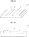
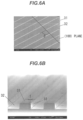
- FIGS.3A and 3B are a perspective view and a side view which show a portion of the principal surface of a ⁇ -Ga 2 O 3 single crystal substrate 30 used for evaluation.
- an upper surface of a mesa portion is defined as a surface 31, a bottom surface of a recessed portion as a surface 32 , and side surfaces of the mesa portion as surfaces 33 and 34 .
- the plane orientation of the surfaces 31 and 32 is ( 010 ).
- the surfaces 33 and 34 are perpendicular to the surfaces 31 and 32 and are planes rotated by an angle 0 from a ( 100 ) plane toward a ( 101 ) plane about the [ 010 ] axis.
- the plane orientation of the surface 34 is further rotated by 180° from ⁇ and is equivalent to the plane orientation of the surface 33.
- a ⁇ -Ga 2 O 3 single crystal was epitaxially grown on the ⁇ -Ga 2 O 3 single crystal substrate 30 by the HVPE method while observing the growth of the ⁇ -Ga 2 O 3 single crystal in a direction perpendicular to the surfaces 33 and 34. Then, a relation between the plane orientation of the plane parallel to the [ 010 ] axis and the growth rate of the ⁇ -Ga 2 O 3 single crystal was evaluated.
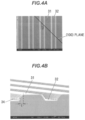
- FIG4A is an image observed in a direction perpendicular to the principal surface and
- FIG.4B is an image observed from obliquely above.
- FIG5A is an image observed in a direction perpendicular to the principal surface and
- FIG5B is an image observed from obliquely above.
- FIG6A is an image observed in a direction perpendicular to the principal surface and
- FIG.6B is an image observed from obliquely above.
- the thickness t shown in FIGS.4B , 5B and 6B indicates a thickness of the ⁇ -Ga 2 O 3 single crystal grown in a direction perpendicular to the surfaces 33 and 34.
- FIG.7 is a graph which is obtained by the evaluation and shows a relation between the growth rate of the ⁇ -Ga 2 O 3 single crystal grown by the HVPE method and the plane orientation of a base substrate.
- the horizontal axis indicates the angle ⁇ of the surface 33 and the vertical axis indicates the growth rate of the ⁇ -Ga 2 O 3 single crystal in a direction perpendicular to the surfaces 33 and 34 (an increase in the thickness t per unit time).
- Plot symbols ⁇ in FIG.7 are the measured values based on the evaluation using the above-mentioned ⁇ -Ga 2 O 3 single crystal substrate 30 .
- Plot symbols ⁇ are the measured values obtained by observing the growth in a direction perpendicular to the principal surface when the ⁇ -Ga 2 O 3 single crystal substrate 30 was not used and a ⁇ -Ga 2 O 3 single crystal was grown on a ⁇ -Ga 2 O 3 single crystal substrate having a flat principal surface with the plane orientation equivalent to the ⁇ -Ga 2 O 3 single crystal substrate 30 .
- the growth rate of the ⁇ -GazOs single crystal in a direction perpendicular to the principal surface was 0.3 ⁇ m/h.
- the growth rate of the ⁇ -Ga 2 O 3 single crystal grown on a plane parallel to the [ 010 ] axis is significantly higher than the growth rate on the ( 010 ) plane in the entire range of 0 ° ⁇ ⁇ ⁇ 180 °.
- the growth rate of the ⁇ -Ga 2 O 3 single crystal is especially high in the range of 38 ° ⁇ ⁇ ⁇ 90 °, as shown in FIG.7 and Table 1.
- the principal surface of the semiconductor substrate 11 of the epitaxial wafer 10 is a plane parallel to the [ 010 ] axis.
- the principal surface of the semiconductor substrate 11 is a plane rotated by an angle within a range of not less than 38 ° and not more than 90 ° from a ( 100 ) plane toward a ( 101 ) plane about the [ 010 ] axis of the P-Ga 2 O 3 -based single crystal.
- the principal surface of the semiconductor substrate 11 is a plane rotated by 68 ⁇ 10 ° from a ( 100 ) plane toward a ( 101 ) plane about the [ 010 ] axis of the P-Ga 2 O 3 -based single crystal.
- MISFET Metal Semiconductor Field Effect Transistor
- FIG.8 is a vertical cross-sectional view showing a lateral transistor 40 in the second embodiment.
- the lateral transistor 40 includes the epitaxial layer 12 formed on the semiconductor substrate 11 , and a gate electrode 41 , a source electrode 42 and a drain electrode 43 which are provided on the epitaxial layer 12.
- the gate electrode 41 is arranged between the source electrode 42 and the drain electrode 43.
- the source electrode 42 and the drain electrode 43 are in contact with an upper surface of the epitaxial layer 12 (a surface opposite to the surface in contact with the semiconductor substrate 11 ) and form ohmic junctions.
- the gate electrode 41 is in contact with the upper surface of the epitaxial layer 12 and forms a Schottky junction, and a depletion layer is thereby formed in the epitaxial layer 12 under the gate electrode 41.
- the lateral transistor 40 functions as either a normally-off transistor or a normally-on transistor depending on the thickness of this depletion region.
- the semiconductor substrate 11 is formed of a ⁇ -Ga 2 O 3 -based crystal containing a p-type dopant such as Mg, Be, Zn or Fe, and has high electrical resistance.
- the epitaxial layer 12 contains an n-type dopant such as Si or Sn.
- the n-type dopant concentration is higher around the contact portion with the source electrode 42 and the drain electrode 43 than in other portions.
- the thickness of the epitaxial layer 12 is, e.g., 0.1 to 1 ⁇ m.
- the gate electrode 41, the source electrode 42 and the drain electrode 43 are formed of, e.g., a metal such as Au, Al, Ti, Sn, Ge, In, Ni, Co, Pt, W, Mo, Cr, Cu and Pb, an alloy containing two or more of such metals, a conductive compound such as ITO, or a conductive polymer.
- the conductive polymer to be used is, e.g., a polythiophene derivative (PEDOT: poly( 3,4 )-ethylenedioxythiophene) doped with polystyrene sulfonate (PSS) or a polypyrrole derivative doped with TCNA, etc.
- the gate electrode 41 may have a two-layer structure composed of two different metals, e.g., Al/Ti, Au/Ni or Au/Co.
- the thickness of the depletion layer in the epitaxial layer 12 under the gate electrode 41 is changed by controlling bias voltage applied to the gate electrode 41 , thereby controlling a drain current.
- the lateral transistor 40 described above is an example of the semiconductor element including the epitaxial wafer 10 in the first embodiment, and the epitaxial wafer 10 can be used to manufacture various other semiconductor elements.
- MISFET Metal Insulator Semiconductor Field Effect Transistor
- HEMT High Electron Mobility Transistor
- Type and concentration of dopant contained in the semiconductor substrate 11 and the epitaxial layer 12 are appropriately determined according to the type of semiconductor element to be manufactured.
- a semiconductor substrate comprising a ⁇ -Ga 2 O 3 single crystal on which an epitaxial layer comprising a ⁇ -Ga 2 O 3 single crystal can be made to grow at a high growth rate using the HVPE method.
- the epitaxial layer of this epitaxial wafer has a high quality.
- a semiconductor substrate comprising a ⁇ -Ga 2 O 3 single crystal on which an epitaxial layer comprising a ⁇ -Ga 2 O 3 single crystal can be made to grow at a high growth rate using the HVPE method; an epitaxial wafer comprising such semiconductor substrate and an epitaxial layer; and a method for manufacturing such epitaxial wafer.
Landscapes
- Chemical & Material Sciences (AREA)
- Engineering & Computer Science (AREA)
- Materials Engineering (AREA)
- Metallurgy (AREA)
- Organic Chemistry (AREA)
- Crystallography & Structural Chemistry (AREA)
- General Chemical & Material Sciences (AREA)
- Chemical Kinetics & Catalysis (AREA)
- Inorganic Chemistry (AREA)
- Mechanical Engineering (AREA)
- Crystals, And After-Treatments Of Crystals (AREA)
- Chemical Vapour Deposition (AREA)
Applications Claiming Priority (2)
| Application Number | Priority Date | Filing Date | Title |
|---|---|---|---|
| JP2014097751A JP6253150B2 (ja) | 2014-05-09 | 2014-05-09 | エピタキシャルウエハ及びその製造方法 |
| PCT/JP2015/063523 WO2015170774A1 (ja) | 2014-05-09 | 2015-05-11 | 半導体基板、並びにエピタキシャルウエハ及びその製造方法 |
Publications (3)
| Publication Number | Publication Date |
|---|---|
| EP3141635A1 EP3141635A1 (en) | 2017-03-15 |
| EP3141635A4 EP3141635A4 (en) | 2018-01-10 |
| EP3141635B1 true EP3141635B1 (en) | 2023-05-03 |
Family
ID=54392621
Family Applications (1)
| Application Number | Title | Priority Date | Filing Date |
|---|---|---|---|
| EP15789328.0A Active EP3141635B1 (en) | 2014-05-09 | 2015-05-11 | Semiconductor substrate, epitaxial wafer, and method for manufacturing epitaxial wafer |
Country Status (6)
| Country | Link |
|---|---|
| US (1) | US10676841B2 (enExample) |
| EP (1) | EP3141635B1 (enExample) |
| JP (1) | JP6253150B2 (enExample) |
| CN (1) | CN106471163B (enExample) |
| TW (1) | TWI721945B (enExample) |
| WO (1) | WO2015170774A1 (enExample) |
Families Citing this family (6)
| Publication number | Priority date | Publication date | Assignee | Title |
|---|---|---|---|---|
| JP5984069B2 (ja) * | 2013-09-30 | 2016-09-06 | 株式会社タムラ製作所 | β−Ga2O3系単結晶膜の成長方法、及び結晶積層構造体 |
| JP6744523B2 (ja) * | 2015-12-16 | 2020-08-19 | 株式会社タムラ製作所 | 半導体基板、並びにエピタキシャルウエハ及びその製造方法 |
| CN113614292B (zh) * | 2019-03-28 | 2024-08-23 | 日本碍子株式会社 | 半导体膜 |
| CN113394079A (zh) * | 2021-06-18 | 2021-09-14 | 中国电子科技集团公司第四十六研究所 | 一种采用卤化物气相外延法生长氧化镓外延层的方法 |
| JP7158627B1 (ja) * | 2021-09-03 | 2022-10-21 | 三菱電機株式会社 | 結晶積層構造体、半導体装置、及び、結晶積層構造体の製造方法 |
| WO2024048710A1 (ja) * | 2022-08-31 | 2024-03-07 | 株式会社Flosfia | 結晶膜および結晶膜の製造方法 |
Family Cites Families (14)
| Publication number | Priority date | Publication date | Assignee | Title |
|---|---|---|---|---|
| US7008839B2 (en) * | 2002-03-08 | 2006-03-07 | Matsushita Electric Industrial Co., Ltd. | Method for manufacturing semiconductor thin film |
| US20070134833A1 (en) | 2005-12-14 | 2007-06-14 | Toyoda Gosei Co., Ltd. | Semiconductor element and method of making same |
| JP4680762B2 (ja) | 2005-12-14 | 2011-05-11 | 株式会社光波 | 発光素子及びその製造方法 |
| GB2436398B (en) * | 2006-03-23 | 2011-08-24 | Univ Bath | Growth method using nanostructure compliant layers and HVPE for producing high quality compound semiconductor materials |
| KR100969127B1 (ko) * | 2010-02-18 | 2010-07-09 | 엘지이노텍 주식회사 | 발광 소자, 발광 소자 제조방법 및 발광 소자 패키지 |
| CN101967680B (zh) * | 2010-11-04 | 2012-02-01 | 山东大学 | 一种在氧化镁衬底上制备单斜晶型氧化镓单晶薄膜的方法 |
| JP5543672B2 (ja) | 2011-09-08 | 2014-07-09 | 株式会社タムラ製作所 | 結晶積層構造体 |
| US9461124B2 (en) * | 2011-09-08 | 2016-10-04 | Tamura Corporation | Ga2O3 semiconductor element |
| WO2013035464A1 (ja) * | 2011-09-08 | 2013-03-14 | 株式会社タムラ製作所 | 結晶積層構造体及びその製造方法 |
| CN103782392A (zh) | 2011-09-08 | 2014-05-07 | 株式会社田村制作所 | Ga2O3 系半导体元件 |
| JP2013229554A (ja) * | 2012-03-30 | 2013-11-07 | Mitsubishi Chemicals Corp | 周期表第13族金属窒化物半導体結晶の製造方法、それに用いるノズルおよび製造装置 |
| JP2013227202A (ja) * | 2012-03-30 | 2013-11-07 | Mitsubishi Chemicals Corp | 周期表第13族金属窒化物半導体結晶の製造方法、および、当該製造方法によって得られた周期表第13族金属窒化物半導体結晶を用いた半導体発光デバイス |
| CN103489967B (zh) * | 2013-09-05 | 2016-07-13 | 大连理工大学 | 一种氧化镓外延膜的制备方法及氧化镓外延膜 |
| JP5984069B2 (ja) * | 2013-09-30 | 2016-09-06 | 株式会社タムラ製作所 | β−Ga2O3系単結晶膜の成長方法、及び結晶積層構造体 |
-
2014
- 2014-05-09 JP JP2014097751A patent/JP6253150B2/ja active Active
-
2015
- 2015-05-11 TW TW104114927A patent/TWI721945B/zh active
- 2015-05-11 EP EP15789328.0A patent/EP3141635B1/en active Active
- 2015-05-11 WO PCT/JP2015/063523 patent/WO2015170774A1/ja not_active Ceased
- 2015-05-11 US US15/309,956 patent/US10676841B2/en active Active
- 2015-05-11 CN CN201580024046.XA patent/CN106471163B/zh active Active
Also Published As
| Publication number | Publication date |
|---|---|
| CN106471163B (zh) | 2020-03-24 |
| US20170145590A1 (en) | 2017-05-25 |
| JP2015214448A (ja) | 2015-12-03 |
| EP3141635A4 (en) | 2018-01-10 |
| TW201606114A (zh) | 2016-02-16 |
| WO2015170774A1 (ja) | 2015-11-12 |
| US10676841B2 (en) | 2020-06-09 |
| TWI721945B (zh) | 2021-03-21 |
| CN106471163A (zh) | 2017-03-01 |
| JP6253150B2 (ja) | 2017-12-27 |
| EP3141635A1 (en) | 2017-03-15 |
Similar Documents
| Publication | Publication Date | Title |
|---|---|---|
| US11982016B2 (en) | Method for growing beta-Ga2O3-based single crystal film, and crystalline layered structure | |
| US10985016B2 (en) | Semiconductor substrate, and epitaxial wafer and method for producing same | |
| EP3141635B1 (en) | Semiconductor substrate, epitaxial wafer, and method for manufacturing epitaxial wafer | |
| US10199512B2 (en) | High voltage withstand Ga2O3-based single crystal schottky barrier diode | |
| JP5018423B2 (ja) | Iii族窒化物半導体結晶基板および半導体デバイス | |
| US20110203513A1 (en) | Method of manufacturing silicon carbide substrate | |
| US11094539B2 (en) | Method for manufacturing nitride semiconductor substrate and nitride semiconductor substrate | |
| JP2020073425A (ja) | 結晶積層構造体、及びそれを製造する方法 | |
| US20120104557A1 (en) | Method for manufacturing a group III nitride crystal, method for manufacturing a group III nitride template, group III nitride crystal and group III nitride template | |
| US20240352619A1 (en) | Crystal lamination structure, semiconductor device, and method of manufacturing crystal lamination structure | |
| JP5641029B2 (ja) | Iii族窒化物系電子デバイス | |
| WO2024095640A1 (ja) | 炭化珪素基板、エピタキシャル基板、半導体装置の製造方法および炭化珪素基板の製造方法 | |
| CN118020143A (zh) | 使外延层中的载流子浓度均匀化的方法以及通过该方法制造的结构 | |
| JP2002025921A (ja) | 化合物半導体結晶及びその成長法 |
Legal Events
| Date | Code | Title | Description |
|---|---|---|---|
| STAA | Information on the status of an ep patent application or granted ep patent |
Free format text: STATUS: THE INTERNATIONAL PUBLICATION HAS BEEN MADE |
|
| PUAI | Public reference made under article 153(3) epc to a published international application that has entered the european phase |
Free format text: ORIGINAL CODE: 0009012 |
|
| STAA | Information on the status of an ep patent application or granted ep patent |
Free format text: STATUS: REQUEST FOR EXAMINATION WAS MADE |
|
| 17P | Request for examination filed |
Effective date: 20161209 |
|
| AK | Designated contracting states |
Kind code of ref document: A1 Designated state(s): AL AT BE BG CH CY CZ DE DK EE ES FI FR GB GR HR HU IE IS IT LI LT LU LV MC MK MT NL NO PL PT RO RS SE SI SK SM TR |
|
| AX | Request for extension of the european patent |
Extension state: BA ME |
|
| DAV | Request for validation of the european patent (deleted) | ||
| DAX | Request for extension of the european patent (deleted) | ||
| A4 | Supplementary search report drawn up and despatched |
Effective date: 20171213 |
|
| RIC1 | Information provided on ipc code assigned before grant |
Ipc: C30B 25/20 20060101ALI20171207BHEP Ipc: C30B 29/16 20060101AFI20171207BHEP Ipc: H01L 21/365 20060101ALI20171207BHEP Ipc: C23C 16/40 20060101ALI20171207BHEP Ipc: H01L 21/205 20060101ALI20171207BHEP |
|
| STAA | Information on the status of an ep patent application or granted ep patent |
Free format text: STATUS: EXAMINATION IS IN PROGRESS |
|
| 17Q | First examination report despatched |
Effective date: 20190123 |
|
| RIC1 | Information provided on ipc code assigned before grant |
Ipc: H01L 21/02 20060101ALI20220926BHEP Ipc: C30B 25/20 20060101ALI20220926BHEP Ipc: C30B 29/16 20060101AFI20220926BHEP |
|
| GRAP | Despatch of communication of intention to grant a patent |
Free format text: ORIGINAL CODE: EPIDOSNIGR1 |
|
| STAA | Information on the status of an ep patent application or granted ep patent |
Free format text: STATUS: GRANT OF PATENT IS INTENDED |
|
| INTG | Intention to grant announced |
Effective date: 20221125 |
|
| GRAS | Grant fee paid |
Free format text: ORIGINAL CODE: EPIDOSNIGR3 |
|
| GRAA | (expected) grant |
Free format text: ORIGINAL CODE: 0009210 |
|
| STAA | Information on the status of an ep patent application or granted ep patent |
Free format text: STATUS: THE PATENT HAS BEEN GRANTED |
|
| AK | Designated contracting states |
Kind code of ref document: B1 Designated state(s): AL AT BE BG CH CY CZ DE DK EE ES FI FR GB GR HR HU IE IS IT LI LT LU LV MC MK MT NL NO PL PT RO RS SE SI SK SM TR |
|
| REG | Reference to a national code |
Ref country code: GB Ref legal event code: FG4D |
|
| REG | Reference to a national code |
Ref country code: AT Ref legal event code: REF Ref document number: 1564656 Country of ref document: AT Kind code of ref document: T Effective date: 20230515 Ref country code: CH Ref legal event code: EP |
|
| REG | Reference to a national code |
Ref country code: DE Ref legal event code: R096 Ref document number: 602015083425 Country of ref document: DE |
|
| REG | Reference to a national code |
Ref country code: IE Ref legal event code: FG4D |
|
| REG | Reference to a national code |
Ref country code: LT Ref legal event code: MG9D |
|
| REG | Reference to a national code |
Ref country code: NL Ref legal event code: MP Effective date: 20230503 |
|
| REG | Reference to a national code |
Ref country code: AT Ref legal event code: MK05 Ref document number: 1564656 Country of ref document: AT Kind code of ref document: T Effective date: 20230503 |
|
| PG25 | Lapsed in a contracting state [announced via postgrant information from national office to epo] |
Ref country code: SE Free format text: LAPSE BECAUSE OF FAILURE TO SUBMIT A TRANSLATION OF THE DESCRIPTION OR TO PAY THE FEE WITHIN THE PRESCRIBED TIME-LIMIT Effective date: 20230503 Ref country code: PT Free format text: LAPSE BECAUSE OF FAILURE TO SUBMIT A TRANSLATION OF THE DESCRIPTION OR TO PAY THE FEE WITHIN THE PRESCRIBED TIME-LIMIT Effective date: 20230904 Ref country code: NO Free format text: LAPSE BECAUSE OF FAILURE TO SUBMIT A TRANSLATION OF THE DESCRIPTION OR TO PAY THE FEE WITHIN THE PRESCRIBED TIME-LIMIT Effective date: 20230803 Ref country code: NL Free format text: LAPSE BECAUSE OF FAILURE TO SUBMIT A TRANSLATION OF THE DESCRIPTION OR TO PAY THE FEE WITHIN THE PRESCRIBED TIME-LIMIT Effective date: 20230503 Ref country code: ES Free format text: LAPSE BECAUSE OF FAILURE TO SUBMIT A TRANSLATION OF THE DESCRIPTION OR TO PAY THE FEE WITHIN THE PRESCRIBED TIME-LIMIT Effective date: 20230503 Ref country code: AT Free format text: LAPSE BECAUSE OF FAILURE TO SUBMIT A TRANSLATION OF THE DESCRIPTION OR TO PAY THE FEE WITHIN THE PRESCRIBED TIME-LIMIT Effective date: 20230503 |
|
| PG25 | Lapsed in a contracting state [announced via postgrant information from national office to epo] |
Ref country code: RS Free format text: LAPSE BECAUSE OF FAILURE TO SUBMIT A TRANSLATION OF THE DESCRIPTION OR TO PAY THE FEE WITHIN THE PRESCRIBED TIME-LIMIT Effective date: 20230503 Ref country code: PL Free format text: LAPSE BECAUSE OF FAILURE TO SUBMIT A TRANSLATION OF THE DESCRIPTION OR TO PAY THE FEE WITHIN THE PRESCRIBED TIME-LIMIT Effective date: 20230503 Ref country code: LV Free format text: LAPSE BECAUSE OF FAILURE TO SUBMIT A TRANSLATION OF THE DESCRIPTION OR TO PAY THE FEE WITHIN THE PRESCRIBED TIME-LIMIT Effective date: 20230503 Ref country code: LT Free format text: LAPSE BECAUSE OF FAILURE TO SUBMIT A TRANSLATION OF THE DESCRIPTION OR TO PAY THE FEE WITHIN THE PRESCRIBED TIME-LIMIT Effective date: 20230503 Ref country code: IS Free format text: LAPSE BECAUSE OF FAILURE TO SUBMIT A TRANSLATION OF THE DESCRIPTION OR TO PAY THE FEE WITHIN THE PRESCRIBED TIME-LIMIT Effective date: 20230903 Ref country code: HR Free format text: LAPSE BECAUSE OF FAILURE TO SUBMIT A TRANSLATION OF THE DESCRIPTION OR TO PAY THE FEE WITHIN THE PRESCRIBED TIME-LIMIT Effective date: 20230503 Ref country code: GR Free format text: LAPSE BECAUSE OF FAILURE TO SUBMIT A TRANSLATION OF THE DESCRIPTION OR TO PAY THE FEE WITHIN THE PRESCRIBED TIME-LIMIT Effective date: 20230804 |
|
| PG25 | Lapsed in a contracting state [announced via postgrant information from national office to epo] |
Ref country code: FI Free format text: LAPSE BECAUSE OF FAILURE TO SUBMIT A TRANSLATION OF THE DESCRIPTION OR TO PAY THE FEE WITHIN THE PRESCRIBED TIME-LIMIT Effective date: 20230503 |
|
| REG | Reference to a national code |
Ref country code: CH Ref legal event code: PL |
|
| PG25 | Lapsed in a contracting state [announced via postgrant information from national office to epo] |
Ref country code: SK Free format text: LAPSE BECAUSE OF FAILURE TO SUBMIT A TRANSLATION OF THE DESCRIPTION OR TO PAY THE FEE WITHIN THE PRESCRIBED TIME-LIMIT Effective date: 20230503 |
|
| REG | Reference to a national code |
Ref country code: BE Ref legal event code: MM Effective date: 20230531 |
|
| PG25 | Lapsed in a contracting state [announced via postgrant information from national office to epo] |
Ref country code: SM Free format text: LAPSE BECAUSE OF FAILURE TO SUBMIT A TRANSLATION OF THE DESCRIPTION OR TO PAY THE FEE WITHIN THE PRESCRIBED TIME-LIMIT Effective date: 20230503 Ref country code: SK Free format text: LAPSE BECAUSE OF FAILURE TO SUBMIT A TRANSLATION OF THE DESCRIPTION OR TO PAY THE FEE WITHIN THE PRESCRIBED TIME-LIMIT Effective date: 20230503 Ref country code: RO Free format text: LAPSE BECAUSE OF FAILURE TO SUBMIT A TRANSLATION OF THE DESCRIPTION OR TO PAY THE FEE WITHIN THE PRESCRIBED TIME-LIMIT Effective date: 20230503 Ref country code: LU Free format text: LAPSE BECAUSE OF NON-PAYMENT OF DUE FEES Effective date: 20230511 Ref country code: LI Free format text: LAPSE BECAUSE OF NON-PAYMENT OF DUE FEES Effective date: 20230531 Ref country code: EE Free format text: LAPSE BECAUSE OF FAILURE TO SUBMIT A TRANSLATION OF THE DESCRIPTION OR TO PAY THE FEE WITHIN THE PRESCRIBED TIME-LIMIT Effective date: 20230503 Ref country code: DK Free format text: LAPSE BECAUSE OF FAILURE TO SUBMIT A TRANSLATION OF THE DESCRIPTION OR TO PAY THE FEE WITHIN THE PRESCRIBED TIME-LIMIT Effective date: 20230503 Ref country code: CZ Free format text: LAPSE BECAUSE OF FAILURE TO SUBMIT A TRANSLATION OF THE DESCRIPTION OR TO PAY THE FEE WITHIN THE PRESCRIBED TIME-LIMIT Effective date: 20230503 Ref country code: CH Free format text: LAPSE BECAUSE OF NON-PAYMENT OF DUE FEES Effective date: 20230531 |
|
| REG | Reference to a national code |
Ref country code: DE Ref legal event code: R097 Ref document number: 602015083425 Country of ref document: DE |
|
| PG25 | Lapsed in a contracting state [announced via postgrant information from national office to epo] |
Ref country code: MC Free format text: LAPSE BECAUSE OF FAILURE TO SUBMIT A TRANSLATION OF THE DESCRIPTION OR TO PAY THE FEE WITHIN THE PRESCRIBED TIME-LIMIT Effective date: 20230503 |
|
| REG | Reference to a national code |
Ref country code: IE Ref legal event code: MM4A |
|
| PG25 | Lapsed in a contracting state [announced via postgrant information from national office to epo] |
Ref country code: MC Free format text: LAPSE BECAUSE OF FAILURE TO SUBMIT A TRANSLATION OF THE DESCRIPTION OR TO PAY THE FEE WITHIN THE PRESCRIBED TIME-LIMIT Effective date: 20230503 |
|
| PLBE | No opposition filed within time limit |
Free format text: ORIGINAL CODE: 0009261 |
|
| STAA | Information on the status of an ep patent application or granted ep patent |
Free format text: STATUS: NO OPPOSITION FILED WITHIN TIME LIMIT |
|
| 26N | No opposition filed |
Effective date: 20240206 |
|
| PG25 | Lapsed in a contracting state [announced via postgrant information from national office to epo] |
Ref country code: IE Free format text: LAPSE BECAUSE OF NON-PAYMENT OF DUE FEES Effective date: 20230511 |
|
| PG25 | Lapsed in a contracting state [announced via postgrant information from national office to epo] |
Ref country code: IE Free format text: LAPSE BECAUSE OF NON-PAYMENT OF DUE FEES Effective date: 20230511 |
|
| PG25 | Lapsed in a contracting state [announced via postgrant information from national office to epo] |
Ref country code: SI Free format text: LAPSE BECAUSE OF FAILURE TO SUBMIT A TRANSLATION OF THE DESCRIPTION OR TO PAY THE FEE WITHIN THE PRESCRIBED TIME-LIMIT Effective date: 20230503 |
|
| PG25 | Lapsed in a contracting state [announced via postgrant information from national office to epo] |
Ref country code: SI Free format text: LAPSE BECAUSE OF FAILURE TO SUBMIT A TRANSLATION OF THE DESCRIPTION OR TO PAY THE FEE WITHIN THE PRESCRIBED TIME-LIMIT Effective date: 20230503 Ref country code: BE Free format text: LAPSE BECAUSE OF NON-PAYMENT OF DUE FEES Effective date: 20230531 |
|
| PG25 | Lapsed in a contracting state [announced via postgrant information from national office to epo] |
Ref country code: BG Free format text: LAPSE BECAUSE OF FAILURE TO SUBMIT A TRANSLATION OF THE DESCRIPTION OR TO PAY THE FEE WITHIN THE PRESCRIBED TIME-LIMIT Effective date: 20230503 |
|
| PG25 | Lapsed in a contracting state [announced via postgrant information from national office to epo] |
Ref country code: BG Free format text: LAPSE BECAUSE OF FAILURE TO SUBMIT A TRANSLATION OF THE DESCRIPTION OR TO PAY THE FEE WITHIN THE PRESCRIBED TIME-LIMIT Effective date: 20230503 |
|
| PGFP | Annual fee paid to national office [announced via postgrant information from national office to epo] |
Ref country code: DE Payment date: 20250521 Year of fee payment: 11 |
|
| PGFP | Annual fee paid to national office [announced via postgrant information from national office to epo] |
Ref country code: GB Payment date: 20250521 Year of fee payment: 11 |
|
| PGFP | Annual fee paid to national office [announced via postgrant information from national office to epo] |
Ref country code: IT Payment date: 20250527 Year of fee payment: 11 |
|
| PGFP | Annual fee paid to national office [announced via postgrant information from national office to epo] |
Ref country code: FR Payment date: 20250528 Year of fee payment: 11 |
|
| PG25 | Lapsed in a contracting state [announced via postgrant information from national office to epo] |
Ref country code: CY Free format text: LAPSE BECAUSE OF FAILURE TO SUBMIT A TRANSLATION OF THE DESCRIPTION OR TO PAY THE FEE WITHIN THE PRESCRIBED TIME-LIMIT; INVALID AB INITIO Effective date: 20150511 |
|
| PG25 | Lapsed in a contracting state [announced via postgrant information from national office to epo] |
Ref country code: HU Free format text: LAPSE BECAUSE OF FAILURE TO SUBMIT A TRANSLATION OF THE DESCRIPTION OR TO PAY THE FEE WITHIN THE PRESCRIBED TIME-LIMIT; INVALID AB INITIO Effective date: 20150511 |
|
| PG25 | Lapsed in a contracting state [announced via postgrant information from national office to epo] |
Ref country code: TR Free format text: LAPSE BECAUSE OF FAILURE TO SUBMIT A TRANSLATION OF THE DESCRIPTION OR TO PAY THE FEE WITHIN THE PRESCRIBED TIME-LIMIT Effective date: 20230503 |