EP3133291A1 - Puce de commande de ventilateur à courant continu - Google Patents
Puce de commande de ventilateur à courant continu Download PDFInfo
- Publication number
- EP3133291A1 EP3133291A1 EP15780557.3A EP15780557A EP3133291A1 EP 3133291 A1 EP3133291 A1 EP 3133291A1 EP 15780557 A EP15780557 A EP 15780557A EP 3133291 A1 EP3133291 A1 EP 3133291A1
- Authority
- EP
- European Patent Office
- Prior art keywords
- direct
- driver
- control chip
- current fan
- fan control
- Prior art date
- Legal status (The legal status is an assumption and is not a legal conclusion. Google has not performed a legal analysis and makes no representation as to the accuracy of the status listed.)
- Granted
Links
Images

Classifications
-
- F—MECHANICAL ENGINEERING; LIGHTING; HEATING; WEAPONS; BLASTING
- F04—POSITIVE - DISPLACEMENT MACHINES FOR LIQUIDS; PUMPS FOR LIQUIDS OR ELASTIC FLUIDS
- F04D—NON-POSITIVE-DISPLACEMENT PUMPS
- F04D27/00—Control, e.g. regulation, of pumps, pumping installations or pumping systems specially adapted for elastic fluids
- F04D27/004—Control, e.g. regulation, of pumps, pumping installations or pumping systems specially adapted for elastic fluids by varying driving speed
-
- F—MECHANICAL ENGINEERING; LIGHTING; HEATING; WEAPONS; BLASTING
- F04—POSITIVE - DISPLACEMENT MACHINES FOR LIQUIDS; PUMPS FOR LIQUIDS OR ELASTIC FLUIDS
- F04D—NON-POSITIVE-DISPLACEMENT PUMPS
- F04D27/00—Control, e.g. regulation, of pumps, pumping installations or pumping systems specially adapted for elastic fluids
-
- F—MECHANICAL ENGINEERING; LIGHTING; HEATING; WEAPONS; BLASTING
- F04—POSITIVE - DISPLACEMENT MACHINES FOR LIQUIDS; PUMPS FOR LIQUIDS OR ELASTIC FLUIDS
- F04D—NON-POSITIVE-DISPLACEMENT PUMPS
- F04D25/00—Pumping installations or systems
- F04D25/02—Units comprising pumps and their driving means
- F04D25/06—Units comprising pumps and their driving means the pump being electrically driven
- F04D25/0606—Units comprising pumps and their driving means the pump being electrically driven the electric motor being specially adapted for integration in the pump
- F04D25/0666—Units comprising pumps and their driving means the pump being electrically driven the electric motor being specially adapted for integration in the pump a sensor is integrated into the pump/motor design
-
- G—PHYSICS
- G01—MEASURING; TESTING
- G01P—MEASURING LINEAR OR ANGULAR SPEED, ACCELERATION, DECELERATION, OR SHOCK; INDICATING PRESENCE, ABSENCE, OR DIRECTION, OF MOVEMENT
- G01P3/00—Measuring linear or angular speed; Measuring differences of linear or angular speeds
- G01P3/42—Devices characterised by the use of electric or magnetic means
- G01P3/44—Devices characterised by the use of electric or magnetic means for measuring angular speed
- G01P3/48—Devices characterised by the use of electric or magnetic means for measuring angular speed by measuring frequency of generated current or voltage
- G01P3/481—Devices characterised by the use of electric or magnetic means for measuring angular speed by measuring frequency of generated current or voltage of pulse signals
- G01P3/487—Devices characterised by the use of electric or magnetic means for measuring angular speed by measuring frequency of generated current or voltage of pulse signals delivered by rotating magnets
-
- G—PHYSICS
- G01—MEASURING; TESTING
- G01R—MEASURING ELECTRIC VARIABLES; MEASURING MAGNETIC VARIABLES
- G01R33/00—Arrangements or instruments for measuring magnetic variables
- G01R33/02—Measuring direction or magnitude of magnetic fields or magnetic flux
- G01R33/06—Measuring direction or magnitude of magnetic fields or magnetic flux using galvano-magnetic devices
- G01R33/09—Magnetoresistive devices
- G01R33/091—Constructional adaptation of the sensor to specific applications
-
- H—ELECTRICITY
- H01—ELECTRIC ELEMENTS
- H01L—SEMICONDUCTOR DEVICES NOT COVERED BY CLASS H10
- H01L25/00—Assemblies consisting of a plurality of individual semiconductor or other solid state devices ; Multistep manufacturing processes thereof
- H01L25/16—Assemblies consisting of a plurality of individual semiconductor or other solid state devices ; Multistep manufacturing processes thereof the devices being of types provided for in two or more different main groups of groups H01L27/00 - H01L33/00, or in a single subclass of H10K, H10N, e.g. forming hybrid circuits
-
- H—ELECTRICITY
- H10—SEMICONDUCTOR DEVICES; ELECTRIC SOLID-STATE DEVICES NOT OTHERWISE PROVIDED FOR
- H10N—ELECTRIC SOLID-STATE DEVICES NOT OTHERWISE PROVIDED FOR
- H10N50/00—Galvanomagnetic devices
- H10N50/10—Magnetoresistive devices
-
- H—ELECTRICITY
- H10—SEMICONDUCTOR DEVICES; ELECTRIC SOLID-STATE DEVICES NOT OTHERWISE PROVIDED FOR
- H10N—ELECTRIC SOLID-STATE DEVICES NOT OTHERWISE PROVIDED FOR
- H10N50/00—Galvanomagnetic devices
- H10N50/80—Constructional details
-
- H—ELECTRICITY
- H10—SEMICONDUCTOR DEVICES; ELECTRIC SOLID-STATE DEVICES NOT OTHERWISE PROVIDED FOR
- H10N—ELECTRIC SOLID-STATE DEVICES NOT OTHERWISE PROVIDED FOR
- H10N50/00—Galvanomagnetic devices
- H10N50/80—Constructional details
- H10N50/85—Magnetic active materials
-
- H—ELECTRICITY
- H01—ELECTRIC ELEMENTS
- H01L—SEMICONDUCTOR DEVICES NOT COVERED BY CLASS H10
- H01L2224/00—Indexing scheme for arrangements for connecting or disconnecting semiconductor or solid-state bodies and methods related thereto as covered by H01L24/00
- H01L2224/01—Means for bonding being attached to, or being formed on, the surface to be connected, e.g. chip-to-package, die-attach, "first-level" interconnects; Manufacturing methods related thereto
- H01L2224/42—Wire connectors; Manufacturing methods related thereto
- H01L2224/47—Structure, shape, material or disposition of the wire connectors after the connecting process
- H01L2224/48—Structure, shape, material or disposition of the wire connectors after the connecting process of an individual wire connector
- H01L2224/4805—Shape
- H01L2224/4809—Loop shape
- H01L2224/48091—Arched
-
- H—ELECTRICITY
- H01—ELECTRIC ELEMENTS
- H01L—SEMICONDUCTOR DEVICES NOT COVERED BY CLASS H10
- H01L2224/00—Indexing scheme for arrangements for connecting or disconnecting semiconductor or solid-state bodies and methods related thereto as covered by H01L24/00
- H01L2224/01—Means for bonding being attached to, or being formed on, the surface to be connected, e.g. chip-to-package, die-attach, "first-level" interconnects; Manufacturing methods related thereto
- H01L2224/42—Wire connectors; Manufacturing methods related thereto
- H01L2224/47—Structure, shape, material or disposition of the wire connectors after the connecting process
- H01L2224/48—Structure, shape, material or disposition of the wire connectors after the connecting process of an individual wire connector
- H01L2224/481—Disposition
- H01L2224/48135—Connecting between different semiconductor or solid-state bodies, i.e. chip-to-chip
- H01L2224/48145—Connecting between different semiconductor or solid-state bodies, i.e. chip-to-chip the bodies being stacked
Definitions
- the present invention relates to a control chip, and in particular, to a direct-current fan control chip that uses a magnetoresistive sensor.
- cooling fans prevailing on the market are mainly fans that use a brushless direct-current motor.
- the position of a rotor determines which stator coil is to be driven, and the position of stator flux vector has to be synchronous with the position of rotor flux vector, such that the motor operates smoothly.
- it is necessary to know the position of the rotor to determine a stator coil to be driven lots of existing technologies can achieve such an objective, and the most commonly used technology is monitoring the position of the rotor by using a Hall Effect magnetic sensor.
- the Hall Effect sensor is great in size and weight, thus increasing the system cost and reducing the reliability.
- the sensor has poor temperature stability and high power consumption.
- the Tunneling Magnetoresistive (TMR) magnetic sensor is a new magnetoresistive effect sensor that has been applied within the industry in recent years, which senses magnetic fields by using the tunnel magnetoresistive effect of magnetic multi-layer film materials, and has a smaller size, lower power consumption and a broader working range relative to the Hall Effect magnetic sensor. More importantly, compared with the traditional Hall sensor, the TMR sensor has an absolute predominance in terms of temperature stability and is more suitable for applications in environments with greater temperature changes. In a system with obvious heat generation, the range of changes in temperature of an environment where a fan control chip is located is broad, and the TMR sensor is more applicable thereto.
- An objective of the present invention is to overcome the above problems existing in the prior art, so as to provide a direct-current fan control chip with a small size, low cost, low power consumption and broad working range.
- the present invention provides a direct-current fan control chip, wherein the direct-current fan control chip includes a magnetoresistive sensor, a controller, a driver and a substrate, the sensing direction of the magnetoresistive sensor is perpendicular to or parallel to the surface of the direct-current fan control chip, the magnetoresistive sensor provides the controller with a rotor position signal, a rotor speed signal, and a rotor rotation direction signal, the controller outputs a control signal to the driver according to the received signals, after receiving the control signals, the driver outputs a drive signal, and the magnetoresistive sensor, the controller and the driver are all integrated on the substrate.
- the direct-current fan control chip includes a magnetoresistive sensor, a controller, a driver and a substrate, the sensing direction of the magnetoresistive sensor is perpendicular to or parallel to the surface of the direct-current fan control chip, the magnetoresistive sensor provides the controller with a rotor position signal, a rotor speed signal, and a rot
- the magnetoresistive sensor is a single-chip sensor, and is formed by InSb elements, TMR elements, GMR elements or AMR elements that are electrically connected.
- the magnetoresistive sensor is a single-axis sensor, a two-axis sensor or a three-axis sensor.
- the single-axis sensor is an X-axis sensor, a Y-axis sensor or a Z-axis sensor.
- the magnetoresistive sensor, the controller and the driver are separately integrated on the substrate.
- the magnetoresistive sensor, the controller and the driver are stacked.
- the magnetoresistive sensor is located above or beneath the controller.
- the magnetoresistive sensor is located above or beneath the driver.
- the controller and the driver are deposited on the same wafer to form a control driver, the control driver being located on the substrate.
- the controller, the driver and the magnetoresistive sensor are deposited on the same wafer to form an inductive control driver, the inductive control driver being located on the substrate.
- the magnetoresistive sensor is located above or beneath the control driver.
- the direct-current fan control chip further includes the following input and output terminals: a temperature signal input terminal, a drive signal output terminal, an alarm signal output terminal and a programmable I/O terminal, wherein the temperature signal input terminal, the alarm signal output terminal and the programmable I/O terminal are all disposed on the controller, and the drive signal output terminal is disposed on the driver.
- the direct-current fan control chip is packaged in the following forms: SIP (single in-line package), DIP (dual inline package), SOP (small outline package), QFN (quad flat non-leaded package), DFN (dual flat non-leaded package), BGA (Ball Grid Array), LGA (land grid array), PGA (pin-grid array), TO (transistor out-line), QFP (quad flat package), SOT (small out-line transistor), LCC (lead on chip), COB (chip on board), COC (ceramic substrate on chip), CSP (chip scale package), MCM (multi-chip module) or ceramic shell package.
- control signal includes at least one PWM (Pulse Width Modulation) signal.
- PWM Pulse Width Modulation
- the present invention has the following beneficial effects:
- the magnetoresistive sensor is integrated with the controller and the driver, which reduces the size and also reduces the device cost and the assembling cost;
- the magnetoresistive sensor has low power consumption, especially the TMR sensor
- the magnetoresistive sensor represented by the TMR sensor has good temperature stability, a wide dynamic range and high reliability.
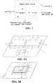
- FIG. 1 is a schematic structural diagram of a direct-current fan control chip in the present invention.
- the control chip includes a magnetoresistive sensor 4, a controller 5 mechanically connected with the magnetoresistive sensor 4, a driver 6 mechanically connected with the controller 5, a substrate 7, a temperature signal input terminal 8, an alarm signal output terminal 9, a drive signal output terminal 10 and a programmable I/O terminal 11.
- the temperature signal input terminal 8, the alarm signal output terminal 9 and the programmable I/O terminal 11 are disposed on the controller 5, and the drive signal output terminal 10 is disposed on the driver 6.
- the magnetoresistive sensor 4 is a single-chip sensor formed by InSb elements, TMR elements, GMR elements or AMR elements that are electrically connected.
- the magnetoresistive sensor 4 may be a single-axis sensor such as an X-axis sensor, a Y-axis sensor or a Z-axis sensor, and may also be a two-axis sensor or a three-axis sensor.
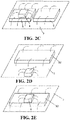
- the magnetoresistive sensor 4, the controller 5 and the driver 6 may be separately integrated on the substrate 7 as shown in FIG. 2A , they may also be integrated on the substrate 7 in a stacked way as shown in FIG. 2B ; however, the upper and lower position relations between them are not limited to those shown in FIG. 2B .
- the magnetoresistive sensor 4 may be placed above or beneath the controller 5 and may also be placed above or beneath the driver 6.
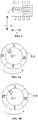
- FIG. 2C shows a situation where the magnetoresistive sensor 4 is placed above the controller 5.
- the controller 5 and the driver 6 may be deposited on the same wafer to form a control driver 12.
- the magnetoresistive sensor 4 may be placed to be separated from the control driver 12 as shown in FIG. 2D , and may also be placed above or beneath the control driver 12.
- FIG. 2E shows a situation where the magnetoresistive sensor 4 is placed above the control driver.
- the magnetoresistive sensor 4, the controller 5 and the driver 6 may also be deposited on the same wafer to form an inductive control driver, and the inductive controller is located on the substrate 7, which is not shown in the figure.
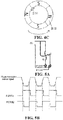
- the sensing direction of the magnetoresistive sensor 4 may be parallel to the surface of the control chip 100 (which is the surface of the packaged chip herein, generally parallel to the surface of the substrate), that is, the direction 1 or 2 in FIG. 3 .
- the position relation between the control chip 100 and a permanent magnet rotor 101 in the fan is as shown in FIG. 4A and FIG. 4B , where the magnetoresistive sensor 4 is an X-axis sensor and a Y-axis sensor.
- the sensing direction of the magnetoresistive sensor 4 may also be perpendicular to the surface of the control chip 100, as shown by the direction 3 in FIG. 3 .
- the position relation between the control chip 100 and the permanent magnet rotor 101 in the fan is as shown in FIG.
- the magnetoresistive sensor 4 is a Z-axis sensor.
- the sensing direction of the control chip 100 is the same as that of the magnetoresistive sensor 4.
- the magnetoresistive sensor 4 transmits a rotor position signal, a rotor speed signal, and a rotor rotation direction signal to the controller 5 according to the operating state of the permanent magnet rotor 101.
- the controller 5 outputs a control signal according to the received signals.
- the controller 5 outputs two PWM signals to the driver 6.
- the driver 6 outputs a drive signal according to the received control signal, that is, the PWM signals, so as to control N-pole and S-pole directions of a stator coil.
- the output of the magnetoresistive sensor 4 determines the output of the driver 6, thus determining the change of the current in the inductor, to control the rotation of the permanent magnet rotor.
- the rotation speed is determined by the duty cycle of an input temperature signal and the PWM signal.
- the direct-current fan control chip in the present invention may be packaged in the following forms: SIP, SOP, QFN, DFN, BGA, LGA, PGA, TO, QFP, SOT, LCC, COB, COC, CSP, MCM, ceramic shell package or the like.
- the direct-current fan control chip is packaged by SOP8 in FIG. 3 .
- the substrate is a metal lead frame.
- the substrate is a PCB.
- the substrate may also be ceramic.
- FIGs. 5A and 5B are a schematic circuit diagram and a phase control sequence diagram respectively.
- the controller 5 After receiving the signals transmitted by the magnetoresistive sensor 4, the controller 5 outputs PWM1 and PWM2 signals to the driver 6. Trigger points of the PWM1 and PWM2 signals are a falling edge and a rising edge of the signals of the magnetoresistive sensor 4, respectively. When the PWM1 and PWM2 signals are triggered, they will be converted from a low level to a high level. At this point, the driver may output a corresponding drive signal to cause the stator coil to change the N-pole and S-pole directions.
- FIGs. 6A-6E are polarity sequence diagrams of stator coils.
- coils L1 and L2 are placed horizontally and vertically, respectively. If the coils L1 and L2 are taken as horizontal and vertical axes and their intersection point is the origin, the magnetoresistive sensor 4 is mounted at the position of 135 degrees of the coordinate axis.
- FIG. 6A indicates that the permanent magnet rotor begins to rotate, and when the permanent magnet rotor rotates to that its N pole and S pole are aligned with the stator coil L2 whose polarity is S pole and the stator coil L1 whose polarity is N pole respectively, the magnetoresistive sensor sends a commutation signal, as shown in FIG. 6B.
- FIG. 6A indicates that the permanent magnet rotor begins to rotate, and when the permanent magnet rotor rotates to that its N pole and S pole are aligned with the stator coil L2 whose polarity is S pole and the stator coil L1 whose polarity is N pole
- FIG. 6C indicates that, after commutation, the permanent magnet rotor continuously rotates, and when the N pole and the S pole of the permanent magnet rotor are aligned with the stator coil L1 whose polarity is S pole and the stator coil L2 whose polarity is N pole respectively once again, the magnetoresistive sensor sends a commutation signal once again, as shown in FIG. 6D.
- FIG. 6E indicates that, after another commutation, the permanent magnet rotor continuously rotates and then can return to the state shown in FIG. 6A , and the process repeats so.
Landscapes
- Engineering & Computer Science (AREA)
- Physics & Mathematics (AREA)
- General Physics & Mathematics (AREA)
- Mechanical Engineering (AREA)
- General Engineering & Computer Science (AREA)
- Microelectronics & Electronic Packaging (AREA)
- Condensed Matter Physics & Semiconductors (AREA)
- Computer Hardware Design (AREA)
- Power Engineering (AREA)
- Control Of Motors That Do Not Use Commutators (AREA)
- Measuring Magnetic Variables (AREA)
- Control Of Positive-Displacement Air Blowers (AREA)
- Brushless Motors (AREA)
Applications Claiming Priority (2)
| Application Number | Priority Date | Filing Date | Title |
|---|---|---|---|
| CN201420178713.2U CN203809329U (zh) | 2014-04-14 | 2014-04-14 | 一种直流风扇控制芯片 |
| PCT/CN2015/076430 WO2015158231A1 (fr) | 2014-04-14 | 2015-04-13 | Puce de commande de ventilateur à courant continu |
Publications (3)
| Publication Number | Publication Date |
|---|---|
| EP3133291A1 true EP3133291A1 (fr) | 2017-02-22 |
| EP3133291A4 EP3133291A4 (fr) | 2018-01-10 |
| EP3133291B1 EP3133291B1 (fr) | 2019-06-26 |
Family
ID=51448087
Family Applications (1)
| Application Number | Title | Priority Date | Filing Date |
|---|---|---|---|
| EP15780557.3A Active EP3133291B1 (fr) | 2014-04-14 | 2015-04-13 | Puce de commande de ventilateur à courant continu |
Country Status (5)
| Country | Link |
|---|---|
| US (1) | US9957967B2 (fr) |
| EP (1) | EP3133291B1 (fr) |
| JP (1) | JP6645985B2 (fr) |
| CN (1) | CN203809329U (fr) |
| WO (1) | WO2015158231A1 (fr) |
Cited By (1)
| Publication number | Priority date | Publication date | Assignee | Title |
|---|---|---|---|---|
| WO2019096865A1 (fr) * | 2017-11-15 | 2019-05-23 | Lem Intellectual Property Sa | Transducteur de commande de courant |
Families Citing this family (2)
| Publication number | Priority date | Publication date | Assignee | Title |
|---|---|---|---|---|
| CN203809329U (zh) | 2014-04-14 | 2014-09-03 | 江苏多维科技有限公司 | 一种直流风扇控制芯片 |
| CN113503266B (zh) * | 2021-05-31 | 2023-04-11 | 阜南县特立电子有限公司 | 一种直流风扇控制系统及直流风扇 |
Family Cites Families (25)
| Publication number | Priority date | Publication date | Assignee | Title |
|---|---|---|---|---|
| JP2975730B2 (ja) * | 1991-07-31 | 1999-11-10 | 三洋電機株式会社 | 混成集積回路装置 |
| JP3004926B2 (ja) * | 1996-12-04 | 2000-01-31 | 株式会社ミツトヨ | 磁気エンコーダ |
| JP2000155038A (ja) * | 1998-11-19 | 2000-06-06 | Mitsubishi Electric Corp | 磁気検出装置 |
| JP3996351B2 (ja) * | 2000-04-03 | 2007-10-24 | 本田技研工業株式会社 | スタータ兼用ジェネレータ |
| US7240254B2 (en) * | 2000-09-21 | 2007-07-03 | Inapac Technology, Inc | Multiple power levels for a chip within a multi-chip semiconductor package |
| US6713909B2 (en) * | 2001-08-20 | 2004-03-30 | James Bryant Money | Digitally controlled variable speed integrated planer motor assembly |
| TW494184B (en) * | 2001-11-14 | 2002-07-11 | Delta Electronics Inc | Fan control system by using a single-chip |
| KR200268109Y1 (ko) * | 2001-12-06 | 2002-03-15 | 김정훈 | 편평형 무정류자 진동모터 |
| US8905721B2 (en) * | 2002-07-12 | 2014-12-09 | Delta Electronics Inc. | Fan control system using a microcontroller |
| US20050184605A1 (en) * | 2004-02-20 | 2005-08-25 | Vinson Wade D. | Cooling fan having three-phase DC motor |
| WO2006117727A1 (fr) * | 2005-05-04 | 2006-11-09 | Nxp B.V. | Dispositif comprenant un module detecteur |
| JP4289401B2 (ja) * | 2007-01-17 | 2009-07-01 | ブラザー工業株式会社 | インクジェット記録装置 |
| US20080218140A1 (en) | 2007-02-08 | 2008-09-11 | Chih-Peng Liao | Control apparatus for cooler |
| US7612553B2 (en) * | 2007-07-26 | 2009-11-03 | Honeywell International Inc. | Current sensor having sandwiched magnetic permeability layer |
| JP5066603B2 (ja) * | 2008-03-04 | 2012-11-07 | アルプス電気株式会社 | 磁気センサ、及び磁気エンコーダ、ならびに磁気センサの製造方法 |
| JP4907629B2 (ja) * | 2008-10-22 | 2012-04-04 | 陞達科技股▲ふん▼有限公司 | ファンのプログラマブルモジュール |
| JP2010268652A (ja) * | 2009-05-18 | 2010-11-25 | Rohm Co Ltd | モータ駆動回路および冷却装置 |
| DE102009042473B4 (de) * | 2009-09-24 | 2019-01-24 | Continental Automotive Gmbh | Verfahren zur Auswertung von Signalen eines Winkelsensors |
| CN102253700A (zh) | 2010-05-20 | 2011-11-23 | 英业达科技有限公司 | 风扇控制系统 |
| JP2012217301A (ja) * | 2011-04-01 | 2012-11-08 | Rohm Co Ltd | ファンモータの駆動装置およびそれを用いた冷却装置、電子機器 |
| CN102797691A (zh) * | 2011-05-27 | 2012-11-28 | 鸿富锦精密工业(深圳)有限公司 | 风扇控制电路 |
| DE202012013636U1 (de) * | 2011-08-06 | 2018-10-29 | Ebm-Papst St. Georgen Gmbh & Co. Kg | Lüfter |
| CN103455114A (zh) | 2012-05-30 | 2013-12-18 | 鸿富锦精密工业(深圳)有限公司 | 服务器机柜散热模组及服务器机柜 |
| CN103244447B (zh) | 2013-05-20 | 2016-06-08 | 上能电气股份有限公司 | 精确检测交流风扇运行状况的故障检测电路及方法 |
| CN203809329U (zh) | 2014-04-14 | 2014-09-03 | 江苏多维科技有限公司 | 一种直流风扇控制芯片 |
-
2014
- 2014-04-14 CN CN201420178713.2U patent/CN203809329U/zh not_active Expired - Lifetime
-
2015
- 2015-04-13 JP JP2016562590A patent/JP6645985B2/ja active Active
- 2015-04-13 EP EP15780557.3A patent/EP3133291B1/fr active Active
- 2015-04-13 US US15/304,285 patent/US9957967B2/en active Active
- 2015-04-13 WO PCT/CN2015/076430 patent/WO2015158231A1/fr active Application Filing
Cited By (1)
| Publication number | Priority date | Publication date | Assignee | Title |
|---|---|---|---|---|
| WO2019096865A1 (fr) * | 2017-11-15 | 2019-05-23 | Lem Intellectual Property Sa | Transducteur de commande de courant |
Also Published As
| Publication number | Publication date |
|---|---|
| WO2015158231A1 (fr) | 2015-10-22 |
| EP3133291A4 (fr) | 2018-01-10 |
| US9957967B2 (en) | 2018-05-01 |
| EP3133291B1 (fr) | 2019-06-26 |
| JP6645985B2 (ja) | 2020-02-14 |
| JP2017514125A (ja) | 2017-06-01 |
| CN203809329U (zh) | 2014-09-03 |
| US20170037859A1 (en) | 2017-02-09 |
Similar Documents
| Publication | Publication Date | Title |
|---|---|---|
| KR102096033B1 (ko) | 스플릿 리드 프레임 및 자석을 포함하는 집적 회로 패키지 | |
| EP3133291B1 (fr) | Puce de commande de ventilateur à courant continu | |
| US11506728B2 (en) | Compact sensor package | |
| EP3467530A1 (fr) | Capteur magnétorésistif à bobine de compensation | |
| CN103944307B (zh) | 一种滑块式线性驱动器 | |
| JP2018537942A5 (fr) | ||
| US10948554B2 (en) | Magnetoresistive sensor package with encapsulated initialization coil | |
| EP2249381A4 (fr) | Puce semi-conductrice et dispositif semi-conducteur | |
| JP2014219386A5 (fr) | ||
| US20170118858A1 (en) | Integrated power module packaging structure | |
| CN203608012U (zh) | 一种滑块式线性驱动器 | |
| US8316552B1 (en) | Systems and methods for three-axis sensor chip packages | |
| KR101231792B1 (ko) | 반도체 패키지 | |
| CN101320082B (zh) | 霍尔磁场元件测试装置 | |
| CN106611758B (zh) | 整合功率模块封装结构 | |
| JP7072265B2 (ja) | ヒステリシス・コイルを有する磁気センサ・パッケージング構造 | |
| US20150185247A1 (en) | Magnet placement for integrated sensor packages | |
| US20130001759A1 (en) | Semiconductor package and method of manufacturing the semiconductor package | |
| CN203553167U (zh) | 一种霍尔混合集成电路的气密性封装结构 | |
| US20110057589A1 (en) | Computer fan control system | |
| JP2002368304A (ja) | ホール素子 | |
| JP2004015946A (ja) | ランドリー機器のモータ駆動回路装置 | |
| EP3376243A1 (fr) | Circuit de capteur magnétique, son procédé de test et procédé de fabrication d'un dispositif semi-conducteur comportant un circuit de capteur magnétique | |
| KR20110077582A (ko) | 일체형 모션 캡처용 6축 센서 및 그 제조 방법 | |
| JPH0537122A (ja) | 混成集積回路装置 |
Legal Events
| Date | Code | Title | Description |
|---|---|---|---|
| STAA | Information on the status of an ep patent application or granted ep patent |
Free format text: STATUS: THE INTERNATIONAL PUBLICATION HAS BEEN MADE |
|
| PUAI | Public reference made under article 153(3) epc to a published international application that has entered the european phase |
Free format text: ORIGINAL CODE: 0009012 |
|
| STAA | Information on the status of an ep patent application or granted ep patent |
Free format text: STATUS: REQUEST FOR EXAMINATION WAS MADE |
|
| 17P | Request for examination filed |
Effective date: 20161103 |
|
| AK | Designated contracting states |
Kind code of ref document: A1 Designated state(s): AL AT BE BG CH CY CZ DE DK EE ES FI FR GB GR HR HU IE IS IT LI LT LU LV MC MK MT NL NO PL PT RO RS SE SI SK SM TR |
|
| AX | Request for extension of the european patent |
Extension state: BA ME |
|
| DAV | Request for validation of the european patent (deleted) | ||
| DAX | Request for extension of the european patent (deleted) | ||
| A4 | Supplementary search report drawn up and despatched |
Effective date: 20171207 |
|
| RIC1 | Information provided on ipc code assigned before grant |
Ipc: F04D 27/00 20060101AFI20171201BHEP |
|
| GRAP | Despatch of communication of intention to grant a patent |
Free format text: ORIGINAL CODE: EPIDOSNIGR1 |
|
| STAA | Information on the status of an ep patent application or granted ep patent |
Free format text: STATUS: GRANT OF PATENT IS INTENDED |
|
| INTG | Intention to grant announced |
Effective date: 20190108 |
|
| GRAS | Grant fee paid |
Free format text: ORIGINAL CODE: EPIDOSNIGR3 |
|
| GRAA | (expected) grant |
Free format text: ORIGINAL CODE: 0009210 |
|
| STAA | Information on the status of an ep patent application or granted ep patent |
Free format text: STATUS: THE PATENT HAS BEEN GRANTED |
|
| AK | Designated contracting states |
Kind code of ref document: B1 Designated state(s): AL AT BE BG CH CY CZ DE DK EE ES FI FR GB GR HR HU IE IS IT LI LT LU LV MC MK MT NL NO PL PT RO RS SE SI SK SM TR |
|
| REG | Reference to a national code |
Ref country code: GB Ref legal event code: FG4D |
|
| REG | Reference to a national code |
Ref country code: CH Ref legal event code: EP |
|
| REG | Reference to a national code |
Ref country code: AT Ref legal event code: REF Ref document number: 1148599 Country of ref document: AT Kind code of ref document: T Effective date: 20190715 |
|
| REG | Reference to a national code |
Ref country code: DE Ref legal event code: R096 Ref document number: 602015032778 Country of ref document: DE |
|
| REG | Reference to a national code |
Ref country code: IE Ref legal event code: FG4D |
|
| REG | Reference to a national code |
Ref country code: NL Ref legal event code: MP Effective date: 20190626 |
|
| PG25 | Lapsed in a contracting state [announced via postgrant information from national office to epo] |
Ref country code: AL Free format text: LAPSE BECAUSE OF FAILURE TO SUBMIT A TRANSLATION OF THE DESCRIPTION OR TO PAY THE FEE WITHIN THE PRESCRIBED TIME-LIMIT Effective date: 20190626 Ref country code: LT Free format text: LAPSE BECAUSE OF FAILURE TO SUBMIT A TRANSLATION OF THE DESCRIPTION OR TO PAY THE FEE WITHIN THE PRESCRIBED TIME-LIMIT Effective date: 20190626 Ref country code: HR Free format text: LAPSE BECAUSE OF FAILURE TO SUBMIT A TRANSLATION OF THE DESCRIPTION OR TO PAY THE FEE WITHIN THE PRESCRIBED TIME-LIMIT Effective date: 20190626 Ref country code: SE Free format text: LAPSE BECAUSE OF FAILURE TO SUBMIT A TRANSLATION OF THE DESCRIPTION OR TO PAY THE FEE WITHIN THE PRESCRIBED TIME-LIMIT Effective date: 20190626 Ref country code: NO Free format text: LAPSE BECAUSE OF FAILURE TO SUBMIT A TRANSLATION OF THE DESCRIPTION OR TO PAY THE FEE WITHIN THE PRESCRIBED TIME-LIMIT Effective date: 20190926 Ref country code: FI Free format text: LAPSE BECAUSE OF FAILURE TO SUBMIT A TRANSLATION OF THE DESCRIPTION OR TO PAY THE FEE WITHIN THE PRESCRIBED TIME-LIMIT Effective date: 20190626 |
|
| REG | Reference to a national code |
Ref country code: LT Ref legal event code: MG4D |
|
| PG25 | Lapsed in a contracting state [announced via postgrant information from national office to epo] |
Ref country code: RS Free format text: LAPSE BECAUSE OF FAILURE TO SUBMIT A TRANSLATION OF THE DESCRIPTION OR TO PAY THE FEE WITHIN THE PRESCRIBED TIME-LIMIT Effective date: 20190626 Ref country code: LV Free format text: LAPSE BECAUSE OF FAILURE TO SUBMIT A TRANSLATION OF THE DESCRIPTION OR TO PAY THE FEE WITHIN THE PRESCRIBED TIME-LIMIT Effective date: 20190626 Ref country code: BG Free format text: LAPSE BECAUSE OF FAILURE TO SUBMIT A TRANSLATION OF THE DESCRIPTION OR TO PAY THE FEE WITHIN THE PRESCRIBED TIME-LIMIT Effective date: 20190926 Ref country code: GR Free format text: LAPSE BECAUSE OF FAILURE TO SUBMIT A TRANSLATION OF THE DESCRIPTION OR TO PAY THE FEE WITHIN THE PRESCRIBED TIME-LIMIT Effective date: 20190927 |
|
| REG | Reference to a national code |
Ref country code: AT Ref legal event code: MK05 Ref document number: 1148599 Country of ref document: AT Kind code of ref document: T Effective date: 20190626 |
|
| PG25 | Lapsed in a contracting state [announced via postgrant information from national office to epo] |
Ref country code: CZ Free format text: LAPSE BECAUSE OF FAILURE TO SUBMIT A TRANSLATION OF THE DESCRIPTION OR TO PAY THE FEE WITHIN THE PRESCRIBED TIME-LIMIT Effective date: 20190626 Ref country code: SK Free format text: LAPSE BECAUSE OF FAILURE TO SUBMIT A TRANSLATION OF THE DESCRIPTION OR TO PAY THE FEE WITHIN THE PRESCRIBED TIME-LIMIT Effective date: 20190626 Ref country code: PT Free format text: LAPSE BECAUSE OF FAILURE TO SUBMIT A TRANSLATION OF THE DESCRIPTION OR TO PAY THE FEE WITHIN THE PRESCRIBED TIME-LIMIT Effective date: 20191028 Ref country code: EE Free format text: LAPSE BECAUSE OF FAILURE TO SUBMIT A TRANSLATION OF THE DESCRIPTION OR TO PAY THE FEE WITHIN THE PRESCRIBED TIME-LIMIT Effective date: 20190626 Ref country code: NL Free format text: LAPSE BECAUSE OF FAILURE TO SUBMIT A TRANSLATION OF THE DESCRIPTION OR TO PAY THE FEE WITHIN THE PRESCRIBED TIME-LIMIT Effective date: 20190626 Ref country code: RO Free format text: LAPSE BECAUSE OF FAILURE TO SUBMIT A TRANSLATION OF THE DESCRIPTION OR TO PAY THE FEE WITHIN THE PRESCRIBED TIME-LIMIT Effective date: 20190626 Ref country code: AT Free format text: LAPSE BECAUSE OF FAILURE TO SUBMIT A TRANSLATION OF THE DESCRIPTION OR TO PAY THE FEE WITHIN THE PRESCRIBED TIME-LIMIT Effective date: 20190626 |
|
| PG25 | Lapsed in a contracting state [announced via postgrant information from national office to epo] |
Ref country code: ES Free format text: LAPSE BECAUSE OF FAILURE TO SUBMIT A TRANSLATION OF THE DESCRIPTION OR TO PAY THE FEE WITHIN THE PRESCRIBED TIME-LIMIT Effective date: 20190626 Ref country code: IS Free format text: LAPSE BECAUSE OF FAILURE TO SUBMIT A TRANSLATION OF THE DESCRIPTION OR TO PAY THE FEE WITHIN THE PRESCRIBED TIME-LIMIT Effective date: 20191026 Ref country code: SM Free format text: LAPSE BECAUSE OF FAILURE TO SUBMIT A TRANSLATION OF THE DESCRIPTION OR TO PAY THE FEE WITHIN THE PRESCRIBED TIME-LIMIT Effective date: 20190626 Ref country code: IT Free format text: LAPSE BECAUSE OF FAILURE TO SUBMIT A TRANSLATION OF THE DESCRIPTION OR TO PAY THE FEE WITHIN THE PRESCRIBED TIME-LIMIT Effective date: 20190626 |
|
| PG25 | Lapsed in a contracting state [announced via postgrant information from national office to epo] |
Ref country code: TR Free format text: LAPSE BECAUSE OF FAILURE TO SUBMIT A TRANSLATION OF THE DESCRIPTION OR TO PAY THE FEE WITHIN THE PRESCRIBED TIME-LIMIT Effective date: 20190626 |
|
| PG25 | Lapsed in a contracting state [announced via postgrant information from national office to epo] |
Ref country code: DK Free format text: LAPSE BECAUSE OF FAILURE TO SUBMIT A TRANSLATION OF THE DESCRIPTION OR TO PAY THE FEE WITHIN THE PRESCRIBED TIME-LIMIT Effective date: 20190626 Ref country code: PL Free format text: LAPSE BECAUSE OF FAILURE TO SUBMIT A TRANSLATION OF THE DESCRIPTION OR TO PAY THE FEE WITHIN THE PRESCRIBED TIME-LIMIT Effective date: 20190626 |
|
| PG25 | Lapsed in a contracting state [announced via postgrant information from national office to epo] |
Ref country code: IS Free format text: LAPSE BECAUSE OF FAILURE TO SUBMIT A TRANSLATION OF THE DESCRIPTION OR TO PAY THE FEE WITHIN THE PRESCRIBED TIME-LIMIT Effective date: 20200224 |
|
| REG | Reference to a national code |
Ref country code: DE Ref legal event code: R097 Ref document number: 602015032778 Country of ref document: DE |
|
| PLBE | No opposition filed within time limit |
Free format text: ORIGINAL CODE: 0009261 |
|
| STAA | Information on the status of an ep patent application or granted ep patent |
Free format text: STATUS: NO OPPOSITION FILED WITHIN TIME LIMIT |
|
| PG2D | Information on lapse in contracting state deleted |
Ref country code: IS |
|
| 26N | No opposition filed |
Effective date: 20200603 |
|
| PG25 | Lapsed in a contracting state [announced via postgrant information from national office to epo] |
Ref country code: SI Free format text: LAPSE BECAUSE OF FAILURE TO SUBMIT A TRANSLATION OF THE DESCRIPTION OR TO PAY THE FEE WITHIN THE PRESCRIBED TIME-LIMIT Effective date: 20190626 |
|
| PG25 | Lapsed in a contracting state [announced via postgrant information from national office to epo] |
Ref country code: MC Free format text: LAPSE BECAUSE OF FAILURE TO SUBMIT A TRANSLATION OF THE DESCRIPTION OR TO PAY THE FEE WITHIN THE PRESCRIBED TIME-LIMIT Effective date: 20190626 |
|
| REG | Reference to a national code |
Ref country code: CH Ref legal event code: PL |
|
| PG25 | Lapsed in a contracting state [announced via postgrant information from national office to epo] |
Ref country code: LI Free format text: LAPSE BECAUSE OF NON-PAYMENT OF DUE FEES Effective date: 20200430 Ref country code: LU Free format text: LAPSE BECAUSE OF NON-PAYMENT OF DUE FEES Effective date: 20200413 Ref country code: CH Free format text: LAPSE BECAUSE OF NON-PAYMENT OF DUE FEES Effective date: 20200430 |
|
| REG | Reference to a national code |
Ref country code: BE Ref legal event code: MM Effective date: 20200430 |
|
| PG25 | Lapsed in a contracting state [announced via postgrant information from national office to epo] |
Ref country code: BE Free format text: LAPSE BECAUSE OF NON-PAYMENT OF DUE FEES Effective date: 20200430 |
|
| PG25 | Lapsed in a contracting state [announced via postgrant information from national office to epo] |
Ref country code: IE Free format text: LAPSE BECAUSE OF NON-PAYMENT OF DUE FEES Effective date: 20200413 |
|
| PG25 | Lapsed in a contracting state [announced via postgrant information from national office to epo] |
Ref country code: MT Free format text: LAPSE BECAUSE OF FAILURE TO SUBMIT A TRANSLATION OF THE DESCRIPTION OR TO PAY THE FEE WITHIN THE PRESCRIBED TIME-LIMIT Effective date: 20190626 Ref country code: CY Free format text: LAPSE BECAUSE OF FAILURE TO SUBMIT A TRANSLATION OF THE DESCRIPTION OR TO PAY THE FEE WITHIN THE PRESCRIBED TIME-LIMIT Effective date: 20190626 |
|
| PG25 | Lapsed in a contracting state [announced via postgrant information from national office to epo] |
Ref country code: MK Free format text: LAPSE BECAUSE OF FAILURE TO SUBMIT A TRANSLATION OF THE DESCRIPTION OR TO PAY THE FEE WITHIN THE PRESCRIBED TIME-LIMIT Effective date: 20190626 |
|
| PGFP | Annual fee paid to national office [announced via postgrant information from national office to epo] |
Ref country code: FR Payment date: 20230425 Year of fee payment: 9 Ref country code: DE Payment date: 20230427 Year of fee payment: 9 |
|
| P01 | Opt-out of the competence of the unified patent court (upc) registered |
Effective date: 20230626 |
|
| PGFP | Annual fee paid to national office [announced via postgrant information from national office to epo] |
Ref country code: GB Payment date: 20230427 Year of fee payment: 9 |