EP3115995A1 - Halbleiterspeichervorrichtung, verfahren zur reparatur einer schlechten spalte und einstellverfahren zur einstellung redundanter informationen davon - Google Patents
Halbleiterspeichervorrichtung, verfahren zur reparatur einer schlechten spalte und einstellverfahren zur einstellung redundanter informationen davon Download PDFInfo
- Publication number
- EP3115995A1 EP3115995A1 EP16178002.8A EP16178002A EP3115995A1 EP 3115995 A1 EP3115995 A1 EP 3115995A1 EP 16178002 A EP16178002 A EP 16178002A EP 3115995 A1 EP3115995 A1 EP 3115995A1
- Authority
- EP
- European Patent Office
- Prior art keywords
- column
- col
- bad
- redundant
- failure
- Prior art date
- Legal status (The legal status is an assumption and is not a legal conclusion. Google has not performed a legal analysis and makes no representation as to the accuracy of the status listed.)
- Granted
Links
Images


Classifications
-
- G—PHYSICS
- G11—INFORMATION STORAGE
- G11C—STATIC STORES
- G11C29/00—Checking stores for correct operation ; Subsequent repair; Testing stores during standby or offline operation
- G11C29/70—Masking faults in memories by using spares or by reconfiguring
- G11C29/78—Masking faults in memories by using spares or by reconfiguring using programmable devices
- G11C29/80—Masking faults in memories by using spares or by reconfiguring using programmable devices with improved layout
- G11C29/808—Masking faults in memories by using spares or by reconfiguring using programmable devices with improved layout using a flexible replacement scheme
-
- G—PHYSICS
- G11—INFORMATION STORAGE
- G11C—STATIC STORES
- G11C29/00—Checking stores for correct operation ; Subsequent repair; Testing stores during standby or offline operation
- G11C29/70—Masking faults in memories by using spares or by reconfiguring
- G11C29/78—Masking faults in memories by using spares or by reconfiguring using programmable devices
- G11C29/785—Masking faults in memories by using spares or by reconfiguring using programmable devices with redundancy programming schemes
-
- G—PHYSICS
- G11—INFORMATION STORAGE
- G11C—STATIC STORES
- G11C29/00—Checking stores for correct operation ; Subsequent repair; Testing stores during standby or offline operation
- G11C29/70—Masking faults in memories by using spares or by reconfiguring
- G11C29/76—Masking faults in memories by using spares or by reconfiguring using address translation or modifications
-
- G—PHYSICS
- G11—INFORMATION STORAGE
- G11C—STATIC STORES
- G11C16/00—Erasable programmable read-only memories
- G11C16/02—Erasable programmable read-only memories electrically programmable
- G11C16/06—Auxiliary circuits, e.g. for writing into memory
- G11C16/08—Address circuits; Decoders; Word-line control circuits
-
- G—PHYSICS
- G11—INFORMATION STORAGE
- G11C—STATIC STORES
- G11C16/00—Erasable programmable read-only memories
- G11C16/02—Erasable programmable read-only memories electrically programmable
- G11C16/06—Auxiliary circuits, e.g. for writing into memory
- G11C16/10—Programming or data input circuits
-
- G—PHYSICS
- G11—INFORMATION STORAGE
- G11C—STATIC STORES
- G11C16/00—Erasable programmable read-only memories
- G11C16/02—Erasable programmable read-only memories electrically programmable
- G11C16/06—Auxiliary circuits, e.g. for writing into memory
- G11C16/34—Determination of programming status, e.g. threshold voltage, overprogramming or underprogramming, retention
- G11C16/3404—Convergence or correction of memory cell threshold voltages; Repair or recovery of overerased or overprogrammed cells
-
- G—PHYSICS
- G11—INFORMATION STORAGE
- G11C—STATIC STORES
- G11C16/00—Erasable programmable read-only memories
- G11C16/02—Erasable programmable read-only memories electrically programmable
- G11C16/06—Auxiliary circuits, e.g. for writing into memory
- G11C16/34—Determination of programming status, e.g. threshold voltage, overprogramming or underprogramming, retention
- G11C16/3436—Arrangements for verifying correct programming or erasure
- G11C16/3454—Arrangements for verifying correct programming or for detecting overprogrammed cells
- G11C16/3459—Circuits or methods to verify correct programming of nonvolatile memory cells
-
- G—PHYSICS
- G11—INFORMATION STORAGE
- G11C—STATIC STORES
- G11C29/00—Checking stores for correct operation ; Subsequent repair; Testing stores during standby or offline operation
- G11C29/04—Detection or location of defective memory elements, e.g. cell constructio details, timing of test signals
- G11C29/08—Functional testing, e.g. testing during refresh, power-on self testing [POST] or distributed testing
- G11C29/12—Built-in arrangements for testing, e.g. built-in self testing [BIST] or interconnection details
- G11C29/44—Indication or identification of errors, e.g. for repair
-
- G—PHYSICS
- G11—INFORMATION STORAGE
- G11C—STATIC STORES
- G11C29/00—Checking stores for correct operation ; Subsequent repair; Testing stores during standby or offline operation
- G11C29/70—Masking faults in memories by using spares or by reconfiguring
- G11C29/78—Masking faults in memories by using spares or by reconfiguring using programmable devices
- G11C29/80—Masking faults in memories by using spares or by reconfiguring using programmable devices with improved layout
- G11C29/816—Masking faults in memories by using spares or by reconfiguring using programmable devices with improved layout for an application-specific layout
- G11C29/82—Masking faults in memories by using spares or by reconfiguring using programmable devices with improved layout for an application-specific layout for EEPROMs
-
- G—PHYSICS
- G11—INFORMATION STORAGE
- G11C—STATIC STORES
- G11C16/00—Erasable programmable read-only memories
- G11C16/02—Erasable programmable read-only memories electrically programmable
- G11C16/04—Erasable programmable read-only memories electrically programmable using variable threshold transistors, e.g. FAMOS
- G11C16/0483—Erasable programmable read-only memories electrically programmable using variable threshold transistors, e.g. FAMOS comprising cells having several storage transistors connected in series
Definitions
- the invention relates to a semiconductor memory device, and particularly relates to a semiconductor memory device repairing a bad column by using a redundant memory.
- a redundancy scheme exists to repair apparent physical defect of a memory element occurring during a manufacturing process.
- a redundancy scheme may include an address conversion circuit and a redundant memory region. Wherein the address conversion circuit converts an address of the memory element having the physical defect to an address of a memory element in the redundant memory region. Accordingly, the redundant memory region serves to repair the defective memory element.
- the address information of the defective memory and the memory element in the redundant memory region is stored in a fuse read only memory (ROM) or a register during a test for the memory chip or when the memory chip is shipped.
- ROM read only memory
- An NAND type flash memory has a memory array.
- the memory array has NAND strings each including a plurality of memory cells that are serially connected.
- one page of data are read from or programmed (written) to the memory array as a unit through a page buffer/sense circuit.
- a method of dividing a page into an odd page and an even page is adopted.
- the flash memory when a column of the memory array has a failure (e.g., a short circuit or an open circuit), the even column and the odd column of the column including the failure are set as a set of bad columns, and the set of bad columns are repaired by using a set of redundant columns in the redundant memory region.
- FIGs. 1(A) and 1(B) are views illustrating a conventional method for repairing a bad column of a flash memory.
- the memory array has a column address Col_0 having an even column e and an odd column o, a column address Col_1 having an even column e and an odd column o, and a column address Col_2 having an even column e and an odd column o.
- a failure F e.g., short circuit
- a set of an even column e and an odd column o in a redundant column address Red_0 in the redundant memory region is used to repair the set of the even column e and the odd column o of the column address Col_2 containing failure.
- the even column e in the column address Col_1 and the odd column o in the column address Col_2 are actually not defective and do not need to be repaired. Since the even column e in the column address Col_1 and the odd column o in the column address Col_2 that are not defective are also repaired, there is a waste in the repairing process of the redundant memory region, so the repair efficiency is lowered, and more redundant memory is consequently needed, thereby making the cost of the flash memory increase.
- the invention provides a semiconductor memory device can improve an efficiency of adopting a redundant memory to repair bad columns.
- An embodiment of the invention provides a semiconductor memory device.
- the semiconductor memory device includes a memory array, a redundant information memory section, and a column selection control circuit.
- the memory array has a memory region including a plurality of memory cells and a redundant memory region including a plurality of memory cells.
- a column address of each column in the memory array corresponds to a set of an even column and an odd column.
- the redundant information memory section stores redundant information, wherein the redundant information includes an address of a bad column, identification information for identifying a failure in which one of the even column or the odd column of the bad column, and an address of a redundant column of the redundant memory region for repairing the bad column.
- the column selection control circuit selects a column of the memory array according to the column address.
- the column selection control circuit determines whether the column address is consistent with the address of the bad column based on the redundant information. When the column address and the address of the bad column are consistent, a column of the bad column having the failure is converted into a column of the redundant column based on the identification information, and another column of the bad column without the failure is not converted into another column of the redundant column.
- the column of the bad column having the failure is an odd column, while the another column of the bad column without the failure is an even column.
- the column of the bad column having the failure is an even column, while the another column of the bad column without the failure is an odd column.
- the column selection control circuit determines whether a failure exists in the even column or the odd column based on the identification information.
- the semiconductor memory device further includes a page buffer, the page buffer keeps data read from the selected page of the memory array or keeps data programmed to the selected page, and the column selection control circuit selects data kept in the odd page or the even page in the page buffer.
- the redundant information includes addresses of a first bad column and a second bad column, when two column addresses of two adjacent columns are consistent with the addresses of the first bad column and the second bad column, one of the even column and the odd column of the first bad column having the failure is converted into the column of the redundant column based on the identification information, and the other one of the even column and the odd column of the first bad column without the failure is not converted into the another column of the redundant column, while one of the even column and the odd column of the second bad column not only having the failure but also adjacent to the column of the first bad column having the failure is converted into the another column of the redundant column.
- An embodiment of the invention provides a method for repairing a bad column of a semiconductor memory device including a memory array and a redundant information memory section.
- the memory array has a memory region including a plurality of memory cells and a redundant memory region including a plurality of memory cells.
- the method for repairing a bad column includes steps as follows: storing redundant information in the redundant information memory section, the redundant information comprises an address of a bad column including an even column and an odd column set as a set, an address of a redundant column in the redundant memory region for repairing the bad column, and identification information identifying a failure in which one of the even column or the odd column of the bad column; and selecting a column of the memory array.
- the step of selecting includes steps as follows: determining whether a column address of the column is consistent with the address of the bad column based on the redundant information; converting a column of the bad column having the failure into a column of the redundant column based on the identification information when the column address and the address of the bad column are consistent, and not converting another column of the bad column without the failure into another column of the redundant column.
- the step of selecting includes determining whether a failure exists in the even column or the odd column based on the identification information during a period of selecting an odd page or an even page.
- An embodiment of the invention provides a setting method for setting redundant information of a semiconductor memory device having a memory array.
- the memory array includes a memory region having a plurality of memory cells and a redundant memory region having a plurality of memory cells.
- the setting method includes steps as follows: detecting an address of a bad column; identifying a failure in one of an even column and an odd column of the bad column, and generating identification information according to a type or a combination of the failure; and setting the identification information and an address of a redundant column used to convert the detected bad column into a redundant column of the redundant memory region in the semiconductor memory device.
- the combination of the failure identifies a failure crossing the even column of a first bad column and the odd column of a second bad column or a failure crossing the odd column of the first bad column and the even column of the second bad column.
- the identification information identifying which one of the even column or the odd column of the bad column has a failure is stored as the redundant information, and the bad column is repaired by using the redundant column based on the identification information.
- unnecessary repair to the even column or the odd column that does not have a failure may be eliminated, so as to improve a repair efficiency of the redundant memory.
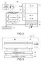
- FIG. 2 is a view illustrating a configuration of an NAND type flash memory according to an embodiment of the invention.
- a flash memory 100 of this embodiment includes a memory array 110 comprising a plurality of memory cells arranged in a matrix, an input/output buffer 120 connected to an external input/output terminal I/O and keeping inputting and outputting data, an address register 130 receiving address data from the input/output buffer 120, a control section 140 receiving command data from the input/output buffer 120 or receiving an external signal to control respective parts of the flash memory 100, a redundant information memory section 150 storing redundant information relating to a bad column of the memory array 110 or a redundant column of the memory array 110 for repairing the bad column, a word line selection circuit 160 receiving row address information Ax from the address register 130 and selecting a block and a word line based on a decoding result of the row address information Ax, a page buffer/sensing circuit 170 keeping data read from a page selected by the word line selection circuit 160 or keeping data written to the selected page,
- the memory array 110 includes m memory blocks, i.e., memory block BLK(0), memory block BLK(1)...memory block BLK(m-1) arranged along a column direction.
- FIG. 3 is a view illustrating a configuration of a memory block.
- the memory array 110 includes a memory region MM where memory cells for regular data reading and writing are configured and a redundant memory area MR where redundant memory cells for repairing a bad column in the memory region MM are configured.
- One memory block includes a plurality of pages, and the memory cells of the memory region MM and the memory cells of the redundant memory region MR are included in a page.
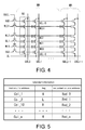
- FIG. 4 illustrates an example of NAND strings formed in a memory block.
- a memory block is formed by arranging a plurality of NAND strings NU in a row direction, and the NAND strings NU includes a plurality of memory cells serially connected.
- one memory block includes n columns (bits) of the NAND strings NU, and a portion of the NAND strings NU are assigned to the redundant memory region MR.
- one page includes 2 K bytes, and 64 bytes of the 2 K bytes are assigned to the redundant memory region MR.
- Bit lines GBL0, GBL2, GBL4...GBLn-2 in even numbers form even pages
- bit lines GBL1, GBL3, GBL5...GBLn-1 in odd numbers form add pages.
- One NAND string NU includes 32 serially connected memory cells MC0 ⁇ MC31, a source side selection transistor SEL_S, and a drain side selection transistor SEL_D, for example. Gates of the memory cells MC0 ⁇ MC31 are respectively connected to corresponding word line WL0 to word line WL31, gates of the source side selection transistor SEL_S and the drain side selection transistor SEL_D are respectively connected to a source side selection line SGS and a drain side selection line SGD. In addition, the source side selection transistor SEL_S is connected to a common source line SL, and a drain side selection transistor SEL_D is connected to a corresponding bit line GBL (GBL0 ⁇ GBLn-1).
- the word line WL0 to the word line WL31, the source side selection line SGS and the drain side selection line SGD are connected to the word line selection circuit 160 through commonly input to a gate of a block selection transistor from a block selection line BSEL.
- the word line selection circuit 160 selects a block through the block selection line BSEL according to the row address information Ax. And based on an operation state, the word line selection circuit 160 suitably drives the source side selection line SGS, the drain side selection line SGD, and the word line WL0 to the word line WL31 of the selected block.
- the memory unit MC0 ⁇ MC31 includes a metal oxide semiconductor (MOS) type transistor, for example.
- the MOS type transistor includes a tunnel oxidation film formed on a channel, a floating gate (charge accumulating layer) that accumulates charges formed on the tunnel oxidation film, and a control gate formed on the floating gate with intervention of a dielectric film.
- a threshold value is in a negative state, and the memory unit is "normally on”.
- the threshold is converted to a positive state, and the memory unit MC0 ⁇ MC31 is "normally off'.
- the memory unit MC0 ⁇ MC31 may be a unit that stores binary data or a unit that stores multilevel data.
- bit line GBL0, the bit line GBL1, ...,the bit line GBLn-1 connected to respective the NAND strings NU are connected to the page buffer/sense circuit 170 through a bit line selection circuit not shown herein.
- the bit line selection circuit may select an even page by an even bit line or an odd page by an odd bit line in reading or programming, and connecting the selected even bit line or odd bit line to the page buffer/sense circuit 170.
- the odd page of the page can be firstly grounded to a reference potential such as GND, and a potential or a current of the bit line of the even page is sensed by the sense circuit.
- the even page is grounded to the reference potential such as GND, and a potential or a current of the bit line of the odd page is sensed by the sense circuit.
- the sense circuit is shared by a pair of an even bit line and an odd bit line. If each of the even page and the odd page forms a page, the page buffer/sense circuit 170 includes a sense circuit for one page and the page buffer keeps data of two pages.
- the page buffer/sense circuit 170 may include a high-speed cache register that keeps the same data as that of the page buffer.
- the high-speed cache register is connected to the page buffer through a transmission gate. During a period when the page buffer is connected to the page selected by the memory array, data are input and output through the high-speed cache buffer.
- the redundant information memory section 150 stores address information of a bad column (bad bit line) in the memory region MM or address information of a redundant column that repairs the bad column.
- a bad column is a physical defect in the product to be shipped.
- the bad column includes, for example, a defect such as a short circuit between adjacent columns, an open circuit in a column, or a defect of a memory unit.
- the redundant information includes an address of the bad column, a flag bit for identifying which of the even column or the odd column of the bad column has a failure, and an address of the redundant column for repairing the bad column.
- the redundant information is stored in a fuse ROM or other non-volatile media when the product is shipped, for example.
- FIG. 5 is an example of the redundant information stored by the redundant information memory section 150.
- one bad column including a set of an even column and an odd column is repaired by a redundant column including a set of an even column and an odd column in the redundant memory region MR. That is, the address of a corresponding bad column corresponds to a set of the even column and the odd column, and the flag bit identifies which of the even column and the odd column of the bad column has a failure.
- a flag bit "L" in a low logical level indicates that at least the even column has a failure
- a flag bit "H" in a high logical level indicates that only the odd column has a failure.
- the flag bit "L” indicates that the failure of the bad column starts from the even column
- the flag bit "H” indicates that the failure of the bad column starts from the odd bit.
- a column address Col_1 has the flag bit "H”, so the failure of the column address Col_1 is at the odd column
- a column address Col_2 has the flag bit "L”, so the failure of the column address Col_2 includes the even column.
- the failures of the column address Col_1 and the column address Col_2 demonstrate the situation of the bad columns of FIG. 1(B) .
- the column selection control circuit 180 selects the bit line GBL0 ⁇ GBLn-1 based on the column address information Ay, so as to write data to or read data from the selected bit line. In addition, when the column address information Ay is consistent with the address of the bad column, the column selection control circuit 180 converts the column address information Ay into the address of the redundant column based on the redundant information stored in the redundant information memory section 150. The column selection control circuit 180 determines whether an input column address is consistent with the address of the bad column when a random read or programming operation is performed based on a column address input externally. If consistent, an address pointer is moved to the column address of the redundant address.
- the column selection control circuit 180 determines whether any of column addresses that have increments from a starting column address is consistent with the address of the bad column. If consistent, the address pointer is moved to the column address of the redundant column.
- conversion of the column address differs according to a value of the flag bit that indicates a property of the bad column.
- the flag bit is "L"
- the bad column has a failure that starts from the even column, as shown in FIG.1 (A)
- a set of the even column and the odd column of the redundant column serves to repair a bad column including a set of even column and the odd column.
- the flag bit is "H"
- the bad column has a failure that starts from the odd column.
- the even column of the bad column without a failure is not replaced by the redundant column.
- the repair of the bad column is performed by replacing the odd column of the bad column having a failure with the odd column of the redundant column.
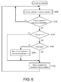
- the control section 140 controls operations of respective parts of the flash memory based on the read command.
- the data kept by the page buffer/sense circuit 170 are continuously read.
- the column selection control circuit 180 makes the address of the starting column provided by the address register 130 increment, while reads the data kept in the page buffer/sense circuit 170 at the same time.
- the increment of the column address may be achieved by moving the address pointer by using software or using an address counter.
- the column selection control circuit 180 can make the column address increment by one by adopting the aforementioned ways (S100), and then determining whether the column address meets the address of the bad column based on the redundant information shown in FIG. 5 (S102).
- the address of the bad column is an address of a column to be repaired or fixed by using the redundant column.
- Step S100 an increment of one of the column address is performed by Step S100.
- the column selection control circuit 180 refers to the flag bit added based on the property of the bad column to determine whether the flag bit is "H" or "L" (S104).
- the column selection control circuit 180 moves the address pointer to the address of the redundant column shown in the redundant information (S108), so as to read the data kept in the redundant column.
- the bad column including the even column and the odd column is directly repaired by the redundant column including the even column and the odd column, so as to move the address pointer by reading a column of the redundant column when reading the even page and reading another column of the redundant column when reading the odd page.
- the column selection control circuit 180 determines whether to perform the read operation of the odd page of the bad column (S106). In the reading operation of the even page of the bad column without the failure, an increment of one of the address of the bad column is performed (S110), and a column of the redundant columns is used to repair the increment address corresponding to the odd column of the bad column having the failure, while in the reading operation of the odd page, an increment of one of the address of the bad column is not performed. Instead, the movement of the address pointer is controlled by using another column of the redundant column for repairing.
- repair of the bad column in this embodiment is similarly performed in other random read operations or random or sequential programming operations.
- FIG. 7 illustrates an example of repairing a bad column.
- the address of the bad column is set as "0110011".
- An upper segment of FIG. 7 indicates the conversion of the column address when the flag bit is "L" (which indicates the even column of the bad column has a failure), and a lower segment of FIG. 7 indicates the conversion of the column address when the flag bit is "H" (which indicates the odd column of the bad column has a failure).
- increments of the column address are performed until the column address is "0110011 ".
- the incremental column address is set as "0110011”
- the address of the bad column is converted to a column address of the redundant column (indicated as "R” in the figure)
- the address of the bad column is converted to another column address of the redundant column (indicated as "R” in the figure).
- the address of the bad column is converted into a column address of the redundant column (indicated as "R" in the figure) for an operation on the odd page.
- R column address of the redundant column
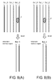
- FIGs. 8(A) and 8(B) are schematic views illustrating repairing a bad column according to this embodiment.
- FIGs. 8(A) and 8(B) respectively correspond to FIGs. 1(A) and 1 (B) .
- the flag bit is "L”
- a redundant column address Red_0 corresponding to a set of an even column and an odd column is used to repair the set of odd column o and even column e of bad column address Col_2.
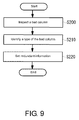
- a test sequence determined in advance by a bad product detecting device or an external controller is performed, so as to detect a bad column of the flash memory (S200). For example, a write operation is performed externally of the chip, and data read from the memory array are compared to the data written for comparison/verification, and a bad column is detected based on a result of verification. Alternatively, with block as a unit, an erase operation is performed based on an erase command, and the bad column is detected based on a result of erasing verification. Then, a type of failure or combination of failures of the detected bad column is identified (S210).
- Which type of identification information is formed may also be determined by a form of operation of the flash memory, such as identifying whether the failure of the bad column exists in the even column or the odd column (such as the flag bit). Alternatively, an operation may be performed to identify a combination of failure from the even column to the odd column or from the odd column to the even column. Then, the redundant information as shown in FIG. 5 is set in the fuse ROM or other non-volatile memory sections in the flash memory (S220).
Landscapes
- For Increasing The Reliability Of Semiconductor Memories (AREA)
- Read Only Memory (AREA)
Applications Claiming Priority (1)
| Application Number | Priority Date | Filing Date | Title |
|---|---|---|---|
| JP2015136735A JP6144729B2 (ja) | 2015-07-08 | 2015-07-08 | 半導体記憶装置 |
Publications (3)
| Publication Number | Publication Date |
|---|---|
| EP3115995A1 true EP3115995A1 (de) | 2017-01-11 |
| EP3115995C0 EP3115995C0 (de) | 2025-04-09 |
| EP3115995B1 EP3115995B1 (de) | 2025-04-09 |
Family
ID=56615819
Family Applications (1)
| Application Number | Title | Priority Date | Filing Date |
|---|---|---|---|
| EP16178002.8A Active EP3115995B1 (de) | 2015-07-08 | 2016-07-05 | Halbleiterspeichervorrichtung, verfahren zur reparatur einer schlechten spalte und einstellverfahren zur einstellung redundanter informationen davon |
Country Status (7)
| Country | Link |
|---|---|
| US (1) | US9627094B2 (de) |
| EP (1) | EP3115995B1 (de) |
| JP (1) | JP6144729B2 (de) |
| KR (1) | KR101771635B1 (de) |
| CN (1) | CN106340324B (de) |
| ES (1) | ES3030458T3 (de) |
| TW (1) | TWI595497B (de) |
Families Citing this family (12)
| Publication number | Priority date | Publication date | Assignee | Title |
|---|---|---|---|---|
| KR101521258B1 (ko) * | 2013-09-10 | 2015-05-21 | 연세대학교 산학협력단 | 메모리 수리 방법 및 메모리 수리 장치 |
| US10002042B2 (en) * | 2015-10-22 | 2018-06-19 | Sandisk Technologies Llc | Systems and methods of detecting errors during read operations and skipping word line portions |
| KR102384864B1 (ko) * | 2017-11-03 | 2022-04-08 | 삼성전자주식회사 | 불량 스트링을 리페어하는 방법 및 불휘발성 메모리 장치 |
| US10971247B2 (en) * | 2018-03-29 | 2021-04-06 | Samsung Electronics Co., Ltd. | Semiconductor memory devices, memory systems, and methods of operating semiconductor memory devices |
| CN110867205B (zh) * | 2018-08-27 | 2021-10-08 | 华邦电子股份有限公司 | 存储器装置以及存储器周边电路 |
| US10908838B2 (en) | 2018-09-25 | 2021-02-02 | Sandisk Technologies Llc | Column replacement with non-dedicated replacement columns |
| US11373726B2 (en) | 2019-04-03 | 2022-06-28 | Texas Instruments Incorporated | Management of multiple memory in-field self-repair options |
| JP7238171B2 (ja) * | 2019-07-12 | 2023-03-13 | 長江存儲科技有限責任公司 | 不良カラム修復を提供するメモリデバイスおよびその動作方法 |
| KR102578438B1 (ko) * | 2020-10-20 | 2023-09-14 | 한양대학교 산학협력단 | 3차원 플래시 메모리에서의 수직 홀 불량 개선 방법 |
| US12374411B2 (en) | 2020-10-20 | 2025-07-29 | Samsung Electronics Co., Ltd. | Three-dimensional flash memory for improving integration and operation method thereof |
| TWI752704B (zh) * | 2020-11-03 | 2022-01-11 | 華邦電子股份有限公司 | 記憶體儲存裝置及其操作方法 |
| US11815995B1 (en) * | 2022-04-27 | 2023-11-14 | Macronix International Co., Ltd. | Redundancy schemes for repairing column defects |
Citations (4)
| Publication number | Priority date | Publication date | Assignee | Title |
|---|---|---|---|---|
| US6122194A (en) * | 1997-12-29 | 2000-09-19 | Samsung Electronics, Co., Ltd. | Semiconductor memory device with a column redundancy occupying a less chip area |
| JP2000311496A (ja) | 1999-04-28 | 2000-11-07 | Nec Corp | 冗長アドレス設定回路及びこれを内蔵した半導体記憶装置 |
| JP2002288993A (ja) | 2001-03-23 | 2002-10-04 | Mitsubishi Electric Corp | 半導体記憶装置 |
| US20130336060A1 (en) * | 2012-06-13 | 2013-12-19 | Winbond Electronics Corp. | Memory device and redundancy method thereof |
Family Cites Families (19)
| Publication number | Priority date | Publication date | Assignee | Title |
|---|---|---|---|---|
| JP2575919B2 (ja) * | 1990-03-22 | 1997-01-29 | 株式会社東芝 | 半導体記憶装置の冗長回路 |
| JP3568265B2 (ja) * | 1995-02-20 | 2004-09-22 | 富士通株式会社 | 半導体メモリ装置 |
| US6199177B1 (en) * | 1998-08-28 | 2001-03-06 | Micron Technology, Inc. | Device and method for repairing a semiconductor memory |
| US6052318A (en) * | 1998-12-22 | 2000-04-18 | Siemens Aktiengesellschaft | Repairable semiconductor memory circuit having parrel redundancy replacement wherein redundancy elements replace failed elements |
| JP2000235800A (ja) | 1999-02-12 | 2000-08-29 | Mitsubishi Electric Corp | 半導体記憶装置 |
| JP2002197888A (ja) * | 2000-12-26 | 2002-07-12 | Sanyo Electric Co Ltd | 半導体記憶装置 |
| JP2002208294A (ja) * | 2001-01-12 | 2002-07-26 | Toshiba Corp | リダンダンシーシステムを有する半導体記憶装置 |
| KR100385956B1 (ko) * | 2001-02-14 | 2003-06-02 | 삼성전자주식회사 | 효율적인 칼럼 리던던시 스킴을 갖는 반도체 메모리장치 |
| TW594775B (en) * | 2001-06-04 | 2004-06-21 | Toshiba Corp | Semiconductor memory device |
| US6704228B2 (en) | 2001-12-28 | 2004-03-09 | Samsung Electronics Co., Ltd | Semiconductor memory device post-repair circuit and method |
| KR100563736B1 (ko) | 2004-01-16 | 2006-03-28 | 주식회사 하이닉스반도체 | 반도체 메모리 소자의 리페어 장치 |
| WO2005081260A1 (ja) * | 2004-02-20 | 2005-09-01 | Spansion Llc | 半導体記憶装置および半導体記憶装置の冗長方法 |
| US7286380B2 (en) * | 2005-09-29 | 2007-10-23 | Intel Corporation | Reconfigurable memory block redundancy to repair defective input/output lines |
| US7949908B2 (en) * | 2006-10-11 | 2011-05-24 | Marvell Israel (M.I.S.L) Ltd. | Memory repair system and method |
| US7996736B2 (en) * | 2008-10-26 | 2011-08-09 | Sandisk 3D Llc | Bad page marking strategy for fast readout in memory |
| US8634261B2 (en) * | 2010-09-06 | 2014-01-21 | SK Hynix Inc. | Semiconductor memory device and method of operating the same |
| US20120075943A1 (en) * | 2010-09-29 | 2012-03-29 | Macronix International Co., Ltd. | Method and Apparatus for Memory Repair With Redundant Columns |
| KR101196907B1 (ko) * | 2010-10-27 | 2012-11-05 | 에스케이하이닉스 주식회사 | 반도체 메모리 장치 및 그의 동작 방법 |
| JP2014186772A (ja) | 2013-03-22 | 2014-10-02 | Toshiba Corp | 半導体記憶装置、コントローラ、及びメモリシステム |
-
2015
- 2015-07-08 JP JP2015136735A patent/JP6144729B2/ja active Active
-
2016
- 2016-06-16 TW TW105118913A patent/TWI595497B/zh active
- 2016-07-05 ES ES16178002T patent/ES3030458T3/es active Active
- 2016-07-05 EP EP16178002.8A patent/EP3115995B1/de active Active
- 2016-07-06 US US15/202,578 patent/US9627094B2/en active Active
- 2016-07-06 CN CN201610527692.4A patent/CN106340324B/zh active Active
- 2016-07-06 KR KR1020160085769A patent/KR101771635B1/ko active Active
Patent Citations (4)
| Publication number | Priority date | Publication date | Assignee | Title |
|---|---|---|---|---|
| US6122194A (en) * | 1997-12-29 | 2000-09-19 | Samsung Electronics, Co., Ltd. | Semiconductor memory device with a column redundancy occupying a less chip area |
| JP2000311496A (ja) | 1999-04-28 | 2000-11-07 | Nec Corp | 冗長アドレス設定回路及びこれを内蔵した半導体記憶装置 |
| JP2002288993A (ja) | 2001-03-23 | 2002-10-04 | Mitsubishi Electric Corp | 半導体記憶装置 |
| US20130336060A1 (en) * | 2012-06-13 | 2013-12-19 | Winbond Electronics Corp. | Memory device and redundancy method thereof |
Also Published As
| Publication number | Publication date |
|---|---|
| EP3115995C0 (de) | 2025-04-09 |
| US20170011809A1 (en) | 2017-01-12 |
| KR20170007154A (ko) | 2017-01-18 |
| JP6144729B2 (ja) | 2017-06-07 |
| CN106340324A (zh) | 2017-01-18 |
| TWI595497B (zh) | 2017-08-11 |
| EP3115995B1 (de) | 2025-04-09 |
| KR101771635B1 (ko) | 2017-08-25 |
| CN106340324B (zh) | 2020-01-21 |
| ES3030458T3 (en) | 2025-06-30 |
| JP2017021872A (ja) | 2017-01-26 |
| TW201715533A (zh) | 2017-05-01 |
| US9627094B2 (en) | 2017-04-18 |
Similar Documents
| Publication | Publication Date | Title |
|---|---|---|
| EP3115995B1 (de) | Halbleiterspeichervorrichtung, verfahren zur reparatur einer schlechten spalte und einstellverfahren zur einstellung redundanter informationen davon | |
| CN103489486B (zh) | 存储器装置以及冗余方法 | |
| US7525839B2 (en) | Semiconductor memory device capable of correcting a read level properly | |
| KR100926195B1 (ko) | 불휘발성 반도체 기억 장치 | |
| JP4976764B2 (ja) | 半導体記憶装置 | |
| US8194465B2 (en) | Non-volatile semiconductor storage device | |
| US8605514B2 (en) | Nonvolatile semiconductor memory device | |
| KR101731576B1 (ko) | 반도체 기억장치 및 nand 플래시 메모리의 프로그램 방법 | |
| JP2009158018A (ja) | 不揮発性半導体記憶装置 | |
| US10395753B2 (en) | Semiconductor memory device and programming method thereof | |
| KR101699476B1 (ko) | 반도체 기억장치 | |
| US9378089B2 (en) | Semiconductor storing device and redundancy method thereof | |
| JP5336053B2 (ja) | 不揮発性メモリ装置及びその動作方法 | |
| US10803954B2 (en) | Memory system | |
| US20120063237A1 (en) | Nonvolatile memory device and method of operating the same | |
| US7558118B2 (en) | NAND flash memory device | |
| CN105321566A (zh) | 半导体存储装置及其编程方法 | |
| JP2010108548A (ja) | 不揮発性半導体記憶装置とその制御方法 | |
| KR101651573B1 (ko) | 반도체 기억장치 및 그 프로그래밍 방법 | |
| TWI478170B (zh) | 記憶體裝置以及冗餘方法 | |
| TWI521530B (zh) | 半導體記憶裝置及其編程方法 |
Legal Events
| Date | Code | Title | Description |
|---|---|---|---|
| PUAI | Public reference made under article 153(3) epc to a published international application that has entered the european phase |
Free format text: ORIGINAL CODE: 0009012 |
|
| STAA | Information on the status of an ep patent application or granted ep patent |
Free format text: STATUS: REQUEST FOR EXAMINATION WAS MADE |
|
| 17P | Request for examination filed |
Effective date: 20160705 |
|
| AK | Designated contracting states |
Kind code of ref document: A1 Designated state(s): AL AT BE BG CH CY CZ DE DK EE ES FI FR GB GR HR HU IE IS IT LI LT LU LV MC MK MT NL NO PL PT RO RS SE SI SK SM TR |
|
| AX | Request for extension of the european patent |
Extension state: BA ME |
|
| STAA | Information on the status of an ep patent application or granted ep patent |
Free format text: STATUS: EXAMINATION IS IN PROGRESS |
|
| 17Q | First examination report despatched |
Effective date: 20200701 |
|
| GRAP | Despatch of communication of intention to grant a patent |
Free format text: ORIGINAL CODE: EPIDOSNIGR1 |
|
| STAA | Information on the status of an ep patent application or granted ep patent |
Free format text: STATUS: GRANT OF PATENT IS INTENDED |
|
| INTG | Intention to grant announced |
Effective date: 20241119 |
|
| GRAS | Grant fee paid |
Free format text: ORIGINAL CODE: EPIDOSNIGR3 |
|
| GRAA | (expected) grant |
Free format text: ORIGINAL CODE: 0009210 |
|
| STAA | Information on the status of an ep patent application or granted ep patent |
Free format text: STATUS: THE PATENT HAS BEEN GRANTED |
|
| AK | Designated contracting states |
Kind code of ref document: B1 Designated state(s): AL AT BE BG CH CY CZ DE DK EE ES FI FR GB GR HR HU IE IS IT LI LT LU LV MC MK MT NL NO PL PT RO RS SE SI SK SM TR |
|
| REG | Reference to a national code |
Ref country code: GB Ref legal event code: FG4D |
|
| REG | Reference to a national code |
Ref country code: CH Ref legal event code: EP |
|
| REG | Reference to a national code |
Ref country code: IE Ref legal event code: FG4D |
|
| U01 | Request for unitary effect filed |
Effective date: 20250409 |
|
| U07 | Unitary effect registered |
Designated state(s): AT BE BG DE DK EE FI FR IT LT LU LV MT NL PT RO SE SI Effective date: 20250415 |
|
| REG | Reference to a national code |
Ref country code: ES Ref legal event code: FG2A Ref document number: 3030458 Country of ref document: ES Kind code of ref document: T3 Effective date: 20250630 |
|
| U20 | Renewal fee for the european patent with unitary effect paid |
Year of fee payment: 10 Effective date: 20250725 |
|
| PGFP | Annual fee paid to national office [announced via postgrant information from national office to epo] |
Ref country code: ES Payment date: 20250812 Year of fee payment: 10 |
|
| PG25 | Lapsed in a contracting state [announced via postgrant information from national office to epo] |
Ref country code: NO Free format text: LAPSE BECAUSE OF FAILURE TO SUBMIT A TRANSLATION OF THE DESCRIPTION OR TO PAY THE FEE WITHIN THE PRESCRIBED TIME-LIMIT Effective date: 20250709 Ref country code: GR Free format text: LAPSE BECAUSE OF FAILURE TO SUBMIT A TRANSLATION OF THE DESCRIPTION OR TO PAY THE FEE WITHIN THE PRESCRIBED TIME-LIMIT Effective date: 20250710 |
|
| PG25 | Lapsed in a contracting state [announced via postgrant information from national office to epo] |
Ref country code: PL Free format text: LAPSE BECAUSE OF FAILURE TO SUBMIT A TRANSLATION OF THE DESCRIPTION OR TO PAY THE FEE WITHIN THE PRESCRIBED TIME-LIMIT Effective date: 20250409 |
|
| PGFP | Annual fee paid to national office [announced via postgrant information from national office to epo] |
Ref country code: GB Payment date: 20250722 Year of fee payment: 10 |
|
| PG25 | Lapsed in a contracting state [announced via postgrant information from national office to epo] |
Ref country code: HR Free format text: LAPSE BECAUSE OF FAILURE TO SUBMIT A TRANSLATION OF THE DESCRIPTION OR TO PAY THE FEE WITHIN THE PRESCRIBED TIME-LIMIT Effective date: 20250409 |
|
| PG25 | Lapsed in a contracting state [announced via postgrant information from national office to epo] |
Ref country code: RS Free format text: LAPSE BECAUSE OF FAILURE TO SUBMIT A TRANSLATION OF THE DESCRIPTION OR TO PAY THE FEE WITHIN THE PRESCRIBED TIME-LIMIT Effective date: 20250709 |
|
| PG25 | Lapsed in a contracting state [announced via postgrant information from national office to epo] |
Ref country code: IS Free format text: LAPSE BECAUSE OF FAILURE TO SUBMIT A TRANSLATION OF THE DESCRIPTION OR TO PAY THE FEE WITHIN THE PRESCRIBED TIME-LIMIT Effective date: 20250809 |
|
| PG25 | Lapsed in a contracting state [announced via postgrant information from national office to epo] |
Ref country code: SM Free format text: LAPSE BECAUSE OF FAILURE TO SUBMIT A TRANSLATION OF THE DESCRIPTION OR TO PAY THE FEE WITHIN THE PRESCRIBED TIME-LIMIT Effective date: 20250409 |
|
| PG25 | Lapsed in a contracting state [announced via postgrant information from national office to epo] |
Ref country code: CZ Free format text: LAPSE BECAUSE OF FAILURE TO SUBMIT A TRANSLATION OF THE DESCRIPTION OR TO PAY THE FEE WITHIN THE PRESCRIBED TIME-LIMIT Effective date: 20250409 |
|
| PG25 | Lapsed in a contracting state [announced via postgrant information from national office to epo] |
Ref country code: SK Free format text: LAPSE BECAUSE OF FAILURE TO SUBMIT A TRANSLATION OF THE DESCRIPTION OR TO PAY THE FEE WITHIN THE PRESCRIBED TIME-LIMIT Effective date: 20250409 |
|
| PLBE | No opposition filed within time limit |
Free format text: ORIGINAL CODE: 0009261 |
|
| STAA | Information on the status of an ep patent application or granted ep patent |
Free format text: STATUS: NO OPPOSITION FILED WITHIN TIME LIMIT |
|
| REG | Reference to a national code |
Ref country code: CH Ref legal event code: L10 Free format text: ST27 STATUS EVENT CODE: U-0-0-L10-L00 (AS PROVIDED BY THE NATIONAL OFFICE) Effective date: 20260218 |
|
| REG | Reference to a national code |
Ref country code: CH Ref legal event code: H13 Free format text: ST27 STATUS EVENT CODE: U-0-0-H10-H13 (AS PROVIDED BY THE NATIONAL OFFICE) Effective date: 20260224 |
|
| 26N | No opposition filed |
Effective date: 20260112 |
|
| PG25 | Lapsed in a contracting state [announced via postgrant information from national office to epo] |
Ref country code: CH Free format text: LAPSE BECAUSE OF NON-PAYMENT OF DUE FEES Effective date: 20250731 |