EP3108499B1 - Bottom package with metal post interconnections - Google Patents
Bottom package with metal post interconnections Download PDFInfo
- Publication number
- EP3108499B1 EP3108499B1 EP15704689.7A EP15704689A EP3108499B1 EP 3108499 B1 EP3108499 B1 EP 3108499B1 EP 15704689 A EP15704689 A EP 15704689A EP 3108499 B1 EP3108499 B1 EP 3108499B1
- Authority
- EP
- European Patent Office
- Prior art keywords
- die
- layer
- substrate
- package
- interconnects
- Prior art date
- Legal status (The legal status is an assumption and is not a legal conclusion. Google has not performed a legal analysis and makes no representation as to the accuracy of the status listed.)
- Active
Links
Images


Classifications
-
- H—ELECTRICITY
- H10—SEMICONDUCTOR DEVICES; ELECTRIC SOLID-STATE DEVICES NOT OTHERWISE PROVIDED FOR
- H10W—GENERIC PACKAGES, INTERCONNECTIONS, CONNECTORS OR OTHER CONSTRUCTIONAL DETAILS OF DEVICES COVERED BY CLASS H10
- H10W72/00—Interconnections or connectors in packages
-
- H—ELECTRICITY
- H05—ELECTRIC TECHNIQUES NOT OTHERWISE PROVIDED FOR
- H05K—PRINTED CIRCUITS; CASINGS OR CONSTRUCTIONAL DETAILS OF ELECTRIC APPARATUS; MANUFACTURE OF ASSEMBLAGES OF ELECTRICAL COMPONENTS
- H05K1/00—Printed circuits
- H05K1/02—Details
- H05K1/09—Use of materials for the conductive, e.g. metallic pattern
-
- H—ELECTRICITY
- H05—ELECTRIC TECHNIQUES NOT OTHERWISE PROVIDED FOR
- H05K—PRINTED CIRCUITS; CASINGS OR CONSTRUCTIONAL DETAILS OF ELECTRIC APPARATUS; MANUFACTURE OF ASSEMBLAGES OF ELECTRICAL COMPONENTS
- H05K1/00—Printed circuits
- H05K1/02—Details
- H05K1/11—Printed elements for providing electric connections to or between printed circuits
- H05K1/115—Via connections; Lands around holes or via connections
-
- H—ELECTRICITY
- H10—SEMICONDUCTOR DEVICES; ELECTRIC SOLID-STATE DEVICES NOT OTHERWISE PROVIDED FOR
- H10W—GENERIC PACKAGES, INTERCONNECTIONS, CONNECTORS OR OTHER CONSTRUCTIONAL DETAILS OF DEVICES COVERED BY CLASS H10
- H10W20/00—Interconnections in chips, wafers or substrates
- H10W20/01—Manufacture or treatment
-
- H—ELECTRICITY
- H10—SEMICONDUCTOR DEVICES; ELECTRIC SOLID-STATE DEVICES NOT OTHERWISE PROVIDED FOR
- H10W—GENERIC PACKAGES, INTERCONNECTIONS, CONNECTORS OR OTHER CONSTRUCTIONAL DETAILS OF DEVICES COVERED BY CLASS H10
- H10W20/00—Interconnections in chips, wafers or substrates
- H10W20/40—Interconnections external to wafers or substrates, e.g. back-end-of-line [BEOL] metallisations or vias connecting to gate electrodes
- H10W20/41—Interconnections external to wafers or substrates, e.g. back-end-of-line [BEOL] metallisations or vias connecting to gate electrodes characterised by their conductive parts
- H10W20/42—Vias, e.g. via plugs
-
- H—ELECTRICITY
- H10—SEMICONDUCTOR DEVICES; ELECTRIC SOLID-STATE DEVICES NOT OTHERWISE PROVIDED FOR
- H10W—GENERIC PACKAGES, INTERCONNECTIONS, CONNECTORS OR OTHER CONSTRUCTIONAL DETAILS OF DEVICES COVERED BY CLASS H10
- H10W20/00—Interconnections in chips, wafers or substrates
- H10W20/40—Interconnections external to wafers or substrates, e.g. back-end-of-line [BEOL] metallisations or vias connecting to gate electrodes
- H10W20/41—Interconnections external to wafers or substrates, e.g. back-end-of-line [BEOL] metallisations or vias connecting to gate electrodes characterised by their conductive parts
- H10W20/43—Layouts of interconnections
-
- H—ELECTRICITY
- H10—SEMICONDUCTOR DEVICES; ELECTRIC SOLID-STATE DEVICES NOT OTHERWISE PROVIDED FOR
- H10W—GENERIC PACKAGES, INTERCONNECTIONS, CONNECTORS OR OTHER CONSTRUCTIONAL DETAILS OF DEVICES COVERED BY CLASS H10
- H10W70/00—Package substrates; Interposers; Redistribution layers [RDL]
- H10W70/01—Manufacture or treatment
- H10W70/05—Manufacture or treatment of insulating or insulated package substrates, or of interposers, or of redistribution layers
- H10W70/093—Connecting or disconnecting other interconnections thereto or therefrom, e.g. connecting bond wires or bumps
-
- H—ELECTRICITY
- H10—SEMICONDUCTOR DEVICES; ELECTRIC SOLID-STATE DEVICES NOT OTHERWISE PROVIDED FOR
- H10W—GENERIC PACKAGES, INTERCONNECTIONS, CONNECTORS OR OTHER CONSTRUCTIONAL DETAILS OF DEVICES COVERED BY CLASS H10
- H10W70/00—Package substrates; Interposers; Redistribution layers [RDL]
- H10W70/01—Manufacture or treatment
- H10W70/05—Manufacture or treatment of insulating or insulated package substrates, or of interposers, or of redistribution layers
- H10W70/095—Manufacture or treatment of insulating or insulated package substrates, or of interposers, or of redistribution layers of vias therein
-
- H—ELECTRICITY
- H10—SEMICONDUCTOR DEVICES; ELECTRIC SOLID-STATE DEVICES NOT OTHERWISE PROVIDED FOR
- H10W—GENERIC PACKAGES, INTERCONNECTIONS, CONNECTORS OR OTHER CONSTRUCTIONAL DETAILS OF DEVICES COVERED BY CLASS H10
- H10W70/00—Package substrates; Interposers; Redistribution layers [RDL]
- H10W70/60—Insulating or insulated package substrates; Interposers; Redistribution layers
- H10W70/611—Insulating or insulated package substrates; Interposers; Redistribution layers for connecting multiple chips together
- H10W70/614—Insulating or insulated package substrates; Interposers; Redistribution layers for connecting multiple chips together the multiple chips being integrally enclosed
-
- H—ELECTRICITY
- H10—SEMICONDUCTOR DEVICES; ELECTRIC SOLID-STATE DEVICES NOT OTHERWISE PROVIDED FOR
- H10W—GENERIC PACKAGES, INTERCONNECTIONS, CONNECTORS OR OTHER CONSTRUCTIONAL DETAILS OF DEVICES COVERED BY CLASS H10
- H10W72/00—Interconnections or connectors in packages
- H10W72/071—Connecting or disconnecting
- H10W72/073—Connecting or disconnecting of die-attach connectors
-
- H—ELECTRICITY
- H10—SEMICONDUCTOR DEVICES; ELECTRIC SOLID-STATE DEVICES NOT OTHERWISE PROVIDED FOR
- H10W—GENERIC PACKAGES, INTERCONNECTIONS, CONNECTORS OR OTHER CONSTRUCTIONAL DETAILS OF DEVICES COVERED BY CLASS H10
- H10W72/00—Interconnections or connectors in packages
- H10W72/20—Bump connectors, e.g. solder bumps or copper pillars; Dummy bumps; Thermal bumps
-
- H—ELECTRICITY
- H10—SEMICONDUCTOR DEVICES; ELECTRIC SOLID-STATE DEVICES NOT OTHERWISE PROVIDED FOR
- H10W—GENERIC PACKAGES, INTERCONNECTIONS, CONNECTORS OR OTHER CONSTRUCTIONAL DETAILS OF DEVICES COVERED BY CLASS H10
- H10W74/00—Encapsulations, e.g. protective coatings
- H10W74/10—Encapsulations, e.g. protective coatings characterised by their shape or disposition
- H10W74/131—Encapsulations, e.g. protective coatings characterised by their shape or disposition the semiconductor body being only partially enclosed
-
- H—ELECTRICITY
- H10—SEMICONDUCTOR DEVICES; ELECTRIC SOLID-STATE DEVICES NOT OTHERWISE PROVIDED FOR
- H10W—GENERIC PACKAGES, INTERCONNECTIONS, CONNECTORS OR OTHER CONSTRUCTIONAL DETAILS OF DEVICES COVERED BY CLASS H10
- H10W90/00—Package configurations
-
- H—ELECTRICITY
- H10—SEMICONDUCTOR DEVICES; ELECTRIC SOLID-STATE DEVICES NOT OTHERWISE PROVIDED FOR
- H10W—GENERIC PACKAGES, INTERCONNECTIONS, CONNECTORS OR OTHER CONSTRUCTIONAL DETAILS OF DEVICES COVERED BY CLASS H10
- H10W90/00—Package configurations
- H10W90/701—Package configurations characterised by the relative positions of pads or connectors relative to package parts
-
- H—ELECTRICITY
- H05—ELECTRIC TECHNIQUES NOT OTHERWISE PROVIDED FOR
- H05K—PRINTED CIRCUITS; CASINGS OR CONSTRUCTIONAL DETAILS OF ELECTRIC APPARATUS; MANUFACTURE OF ASSEMBLAGES OF ELECTRICAL COMPONENTS
- H05K2201/00—Indexing scheme relating to printed circuits covered by H05K1/00
- H05K2201/09—Shape and layout
- H05K2201/09818—Shape or layout details not covered by a single group of H05K2201/09009 - H05K2201/09809
- H05K2201/09845—Stepped hole, via, edge, bump or conductor
-
- H—ELECTRICITY
- H05—ELECTRIC TECHNIQUES NOT OTHERWISE PROVIDED FOR
- H05K—PRINTED CIRCUITS; CASINGS OR CONSTRUCTIONAL DETAILS OF ELECTRIC APPARATUS; MANUFACTURE OF ASSEMBLAGES OF ELECTRICAL COMPONENTS
- H05K2201/00—Indexing scheme relating to printed circuits covered by H05K1/00
- H05K2201/10—Details of components or other objects attached to or integrated in a printed circuit board
- H05K2201/10227—Other objects, e.g. metallic pieces
- H05K2201/10242—Metallic cylinders
-
- H—ELECTRICITY
- H10—SEMICONDUCTOR DEVICES; ELECTRIC SOLID-STATE DEVICES NOT OTHERWISE PROVIDED FOR
- H10W—GENERIC PACKAGES, INTERCONNECTIONS, CONNECTORS OR OTHER CONSTRUCTIONAL DETAILS OF DEVICES COVERED BY CLASS H10
- H10W70/00—Package substrates; Interposers; Redistribution layers [RDL]
- H10W70/60—Insulating or insulated package substrates; Interposers; Redistribution layers
- H10W70/611—Insulating or insulated package substrates; Interposers; Redistribution layers for connecting multiple chips together
-
- H—ELECTRICITY
- H10—SEMICONDUCTOR DEVICES; ELECTRIC SOLID-STATE DEVICES NOT OTHERWISE PROVIDED FOR
- H10W—GENERIC PACKAGES, INTERCONNECTIONS, CONNECTORS OR OTHER CONSTRUCTIONAL DETAILS OF DEVICES COVERED BY CLASS H10
- H10W70/00—Package substrates; Interposers; Redistribution layers [RDL]
- H10W70/60—Insulating or insulated package substrates; Interposers; Redistribution layers
- H10W70/62—Insulating or insulated package substrates; Interposers; Redistribution layers characterised by their interconnections
- H10W70/63—Vias, e.g. via plugs
- H10W70/635—Through-vias
-
- H—ELECTRICITY
- H10—SEMICONDUCTOR DEVICES; ELECTRIC SOLID-STATE DEVICES NOT OTHERWISE PROVIDED FOR
- H10W—GENERIC PACKAGES, INTERCONNECTIONS, CONNECTORS OR OTHER CONSTRUCTIONAL DETAILS OF DEVICES COVERED BY CLASS H10
- H10W70/00—Package substrates; Interposers; Redistribution layers [RDL]
- H10W70/60—Insulating or insulated package substrates; Interposers; Redistribution layers
- H10W70/62—Insulating or insulated package substrates; Interposers; Redistribution layers characterised by their interconnections
- H10W70/65—Shapes or dispositions of interconnections
-
- H—ELECTRICITY
- H10—SEMICONDUCTOR DEVICES; ELECTRIC SOLID-STATE DEVICES NOT OTHERWISE PROVIDED FOR
- H10W—GENERIC PACKAGES, INTERCONNECTIONS, CONNECTORS OR OTHER CONSTRUCTIONAL DETAILS OF DEVICES COVERED BY CLASS H10
- H10W70/00—Package substrates; Interposers; Redistribution layers [RDL]
- H10W70/60—Insulating or insulated package substrates; Interposers; Redistribution layers
- H10W70/67—Insulating or insulated package substrates; Interposers; Redistribution layers characterised by their insulating layers or insulating parts
- H10W70/69—Insulating materials thereof
- H10W70/692—Ceramics or glasses
-
- H—ELECTRICITY
- H10—SEMICONDUCTOR DEVICES; ELECTRIC SOLID-STATE DEVICES NOT OTHERWISE PROVIDED FOR
- H10W—GENERIC PACKAGES, INTERCONNECTIONS, CONNECTORS OR OTHER CONSTRUCTIONAL DETAILS OF DEVICES COVERED BY CLASS H10
- H10W70/00—Package substrates; Interposers; Redistribution layers [RDL]
- H10W70/60—Insulating or insulated package substrates; Interposers; Redistribution layers
- H10W70/67—Insulating or insulated package substrates; Interposers; Redistribution layers characterised by their insulating layers or insulating parts
- H10W70/69—Insulating materials thereof
- H10W70/695—Organic materials
-
- H—ELECTRICITY
- H10—SEMICONDUCTOR DEVICES; ELECTRIC SOLID-STATE DEVICES NOT OTHERWISE PROVIDED FOR
- H10W—GENERIC PACKAGES, INTERCONNECTIONS, CONNECTORS OR OTHER CONSTRUCTIONAL DETAILS OF DEVICES COVERED BY CLASS H10
- H10W70/00—Package substrates; Interposers; Redistribution layers [RDL]
- H10W70/60—Insulating or insulated package substrates; Interposers; Redistribution layers
- H10W70/67—Insulating or insulated package substrates; Interposers; Redistribution layers characterised by their insulating layers or insulating parts
- H10W70/69—Insulating materials thereof
- H10W70/698—Semiconductor materials that are electrically insulating, e.g. undoped silicon
-
- H—ELECTRICITY
- H10—SEMICONDUCTOR DEVICES; ELECTRIC SOLID-STATE DEVICES NOT OTHERWISE PROVIDED FOR
- H10W—GENERIC PACKAGES, INTERCONNECTIONS, CONNECTORS OR OTHER CONSTRUCTIONAL DETAILS OF DEVICES COVERED BY CLASS H10
- H10W72/00—Interconnections or connectors in packages
- H10W72/01—Manufacture or treatment
- H10W72/0198—Manufacture or treatment batch processes
-
- H—ELECTRICITY
- H10—SEMICONDUCTOR DEVICES; ELECTRIC SOLID-STATE DEVICES NOT OTHERWISE PROVIDED FOR
- H10W—GENERIC PACKAGES, INTERCONNECTIONS, CONNECTORS OR OTHER CONSTRUCTIONAL DETAILS OF DEVICES COVERED BY CLASS H10
- H10W72/00—Interconnections or connectors in packages
- H10W72/071—Connecting or disconnecting
- H10W72/072—Connecting or disconnecting of bump connectors
- H10W72/07251—Connecting or disconnecting of bump connectors characterised by changes in properties of the bump connectors during connecting
- H10W72/07254—Connecting or disconnecting of bump connectors characterised by changes in properties of the bump connectors during connecting changes in dispositions
-
- H—ELECTRICITY
- H10—SEMICONDUCTOR DEVICES; ELECTRIC SOLID-STATE DEVICES NOT OTHERWISE PROVIDED FOR
- H10W—GENERIC PACKAGES, INTERCONNECTIONS, CONNECTORS OR OTHER CONSTRUCTIONAL DETAILS OF DEVICES COVERED BY CLASS H10
- H10W72/00—Interconnections or connectors in packages
- H10W72/20—Bump connectors, e.g. solder bumps or copper pillars; Dummy bumps; Thermal bumps
- H10W72/241—Dispositions, e.g. layouts
- H10W72/247—Dispositions of multiple bumps
- H10W72/248—Top-view layouts, e.g. mirror arrays
-
- H—ELECTRICITY
- H10—SEMICONDUCTOR DEVICES; ELECTRIC SOLID-STATE DEVICES NOT OTHERWISE PROVIDED FOR
- H10W—GENERIC PACKAGES, INTERCONNECTIONS, CONNECTORS OR OTHER CONSTRUCTIONAL DETAILS OF DEVICES COVERED BY CLASS H10
- H10W72/00—Interconnections or connectors in packages
- H10W72/20—Bump connectors, e.g. solder bumps or copper pillars; Dummy bumps; Thermal bumps
- H10W72/251—Materials
- H10W72/252—Materials comprising solid metals or solid metalloids, e.g. PbSn, Ag or Cu
-
- H—ELECTRICITY
- H10—SEMICONDUCTOR DEVICES; ELECTRIC SOLID-STATE DEVICES NOT OTHERWISE PROVIDED FOR
- H10W—GENERIC PACKAGES, INTERCONNECTIONS, CONNECTORS OR OTHER CONSTRUCTIONAL DETAILS OF DEVICES COVERED BY CLASS H10
- H10W72/00—Interconnections or connectors in packages
- H10W72/20—Bump connectors, e.g. solder bumps or copper pillars; Dummy bumps; Thermal bumps
- H10W72/29—Bond pads specially adapted therefor
-
- H—ELECTRICITY
- H10—SEMICONDUCTOR DEVICES; ELECTRIC SOLID-STATE DEVICES NOT OTHERWISE PROVIDED FOR
- H10W—GENERIC PACKAGES, INTERCONNECTIONS, CONNECTORS OR OTHER CONSTRUCTIONAL DETAILS OF DEVICES COVERED BY CLASS H10
- H10W72/00—Interconnections or connectors in packages
- H10W72/30—Die-attach connectors
- H10W72/341—Dispositions of die-attach connectors, e.g. layouts
- H10W72/347—Dispositions of multiple die-attach connectors
-
- H—ELECTRICITY
- H10—SEMICONDUCTOR DEVICES; ELECTRIC SOLID-STATE DEVICES NOT OTHERWISE PROVIDED FOR
- H10W—GENERIC PACKAGES, INTERCONNECTIONS, CONNECTORS OR OTHER CONSTRUCTIONAL DETAILS OF DEVICES COVERED BY CLASS H10
- H10W74/00—Encapsulations, e.g. protective coatings
-
- H—ELECTRICITY
- H10—SEMICONDUCTOR DEVICES; ELECTRIC SOLID-STATE DEVICES NOT OTHERWISE PROVIDED FOR
- H10W—GENERIC PACKAGES, INTERCONNECTIONS, CONNECTORS OR OTHER CONSTRUCTIONAL DETAILS OF DEVICES COVERED BY CLASS H10
- H10W74/00—Encapsulations, e.g. protective coatings
- H10W74/10—Encapsulations, e.g. protective coatings characterised by their shape or disposition
- H10W74/131—Encapsulations, e.g. protective coatings characterised by their shape or disposition the semiconductor body being only partially enclosed
- H10W74/142—Encapsulations, e.g. protective coatings characterised by their shape or disposition the semiconductor body being only partially enclosed the encapsulations exposing the passive side of the semiconductor body
-
- H—ELECTRICITY
- H10—SEMICONDUCTOR DEVICES; ELECTRIC SOLID-STATE DEVICES NOT OTHERWISE PROVIDED FOR
- H10W—GENERIC PACKAGES, INTERCONNECTIONS, CONNECTORS OR OTHER CONSTRUCTIONAL DETAILS OF DEVICES COVERED BY CLASS H10
- H10W90/00—Package configurations
- H10W90/701—Package configurations characterised by the relative positions of pads or connectors relative to package parts
- H10W90/721—Package configurations characterised by the relative positions of pads or connectors relative to package parts of bump connectors
- H10W90/722—Package configurations characterised by the relative positions of pads or connectors relative to package parts of bump connectors between stacked chips
-
- H—ELECTRICITY
- H10—SEMICONDUCTOR DEVICES; ELECTRIC SOLID-STATE DEVICES NOT OTHERWISE PROVIDED FOR
- H10W—GENERIC PACKAGES, INTERCONNECTIONS, CONNECTORS OR OTHER CONSTRUCTIONAL DETAILS OF DEVICES COVERED BY CLASS H10
- H10W90/00—Package configurations
- H10W90/701—Package configurations characterised by the relative positions of pads or connectors relative to package parts
- H10W90/721—Package configurations characterised by the relative positions of pads or connectors relative to package parts of bump connectors
- H10W90/724—Package configurations characterised by the relative positions of pads or connectors relative to package parts of bump connectors between a chip and a stacked insulating package substrate, interposer or RDL
Definitions
- This application relates to integrated circuit packaging, and more particularly to a bottom package having metal post interconnections.
- Organic substrates are commonly used in package-on-package architectures because of their low cost.
- a flip-chip die such as a micro-processor may be coupled to a first surface of an organic substrate for a bottom package through a plurality of solder bumps or copper pillars.
- the bottom package substrate has a footprint large enough such that there is perimeter about the bottom package die on the first surface of the bottom package substrate. That perimeter may then support solder ball interconnections to the top package.
- the resulting package-on-package architecture is quite popular due to its low cost, organic substrates are often not suitable for modern fine-pitch dies because an organic substrate accommodates only a relatively coarse interconnect pitch.
- the interconnect pitch is the separation between the substrate-to-die interconnections such as micro-bumps or copper pillars as well as the bottom-package-to-top-package interconnections such as solder balls.
- the bottom package substrate for modern fine-pitch dies typically comprises a glass or semiconductor interposer.
- a glass or semiconductor interposer supports fine-pitch interconnections. It is thus conventional to mount fine-pitch dies onto an interposer because a glass or silicon interposer enables the necessary fine-pitch interconnections.
- Multiple fine-pitch dies such as a first processor die and a second processor die may be mounted on the same interposer.
- the interposer receives the fine-pitch interconnects such as micro-bumps or copper pillars from each die through a redistribution layer (RDL) that enables each die to communicate with the other die(s) through the RDL.
- RDL redistribution layer
- the resulting interposer package is thus advantageous in that it accommodates the necessary fine-pitch interconnections, it is conventional to interface processors with associated external memories such as a DRAM die using a package-on-package (PoP) construction. But the footprint of the interposer is already somewhat large as it must have the necessary surface area to support the fine-pitch dies.
- PoP package-on-package
- interposer also includes a perimeter around the fine-pitch dies to provide space for conventional PoP solder ball interconnections to an upper memory package substrate
- the interposer footprint becomes excessive.
- the encased solder balls must then be exposed such as through the use of laser drilling of the mold compound.
- the heat from the laser requires a certain keep-out distance between the solder balls and the dies.
- the resulting interposer for the bottom package thus requires a relatively large footprint to support not only the dies and the solder balls but also the keep out distance between the solder balls and the dies.
- the solder balls must be relatively large to couple to the upper package.
- Such a relatively large interconnect size requires a correspondingly large interconnect pitch.
- the interposer footprint thus must be large enough to support both the solder balls with their requisite pitch as well as the associated keep-out area between the solder balls and the die, which decreases density and is expensive.
- the interposer may include a perimeter that supports an interconnect bar such as a printed circuit bar or a silicon or glass interconnect bar.
- the interconnect bar includes a number of plated vias as opposed to solder balls. But the manufacture of the plated vias in the interconnect bar also require a certain distance or keep out area with regard to the interconnect bar outer perimeter.
- the interposer footprint must be relatively large.
- US 2013/0187268 A1 describes a package with a substrate. Through substrate vias extend from a first side of the substrate to a second side of the substrate. A first redistribution layer, first contact pads, second contact pads, a first passivation layer, and first UBMs are located on the first side of the substrate. A second redistribution layer, third contacts, second UBMs, and a second passivation layer are located on the second side of the substrate.
- US 2014/0015121 A1 describes a wiring substrate which includes a core substrate made of glass and having a first surface, a second surface opposite to the first surface, a side surface between the first surface and the second surface, an insulating layer and a wiring layer.
- the insulating layer and the wiring layer are formed on at least one of the first surface and the second surface of the core substrate.
- a plurality of concave portions are formed in the side surface of the core substrate to extend from the first surface to the second surface, and a resin is filled in the respective concave portions.
- bottom package substrates such as interposers with reduced footprints.
- a bottom package is provided with plated metal posts for forming interconnects to a top package.
- the plated metal posts enable a reduced footprint for the bottom package as compared to conventional bottom packages that use solder balls or interconnect bars to form the interconnections to an upper package or additional die.
- the bottom package includes a bottom package substrate supporting one or more dies.
- the bottom package substrate may comprise a glass, silicon, or laminated organic interposer that supports a plurality of dies.
- the bottom package substrate may comprise a glass substrate, a semiconductor substrate, or a laminated organic substrate that supports a single die.
- the bottom package substrate includes a plurality of plated metal posts coupled to die interconnects through a redistribution layer (RDL).
- the die(s) supported by the bottom package substrate couple through the die interconnects to the RDL, from the RDL to the metal posts, and from the metal posts to a top package substrate.
- both the metal posts and the die interconnects are plated onto a seed layer overlaying the RDL.
- the die interconnects and metal posts may be plated onto the seed layer prior to attachment of the die (or dies) to the bottom package substrate.
- the metal posts may thus be deposited without any need for a keep out area in contrast to conventional bar interconnect or solder ball embodiments.
- the resulting bottom package substrates disclosed herein thus have advantageously enhanced density as compared to conventional architectures.
- a bottom package is provided with plated metal posts for forming the interconnects to the top package.
- the plated metal posts enable a reduced footprint for the bottom package as compared to the conventional bottom packages that use solder balls or interconnect bars to form the interconnections to an upper package or additional die.
- the bottom package includes a bottom package substrate supporting one or more dies.
- the bottom package substrate may comprise a glass, silicon, or laminated organic interposer that supports a plurality of dies.
- the bottom package substrate may comprise a glass, semiconductor, or laminated organic substrate that supports a single die.
- the metal posts disclosed herein are plated on the bottom package substrate, manufacturing costs are considerably reduced as compared to the conventional use of interconnect bars, which requires the extra process steps of embedding the interconnect bar in the bottom package substrate.
- the interconnect bar manufacture typically requires laser drilling of the vias that are then plated to form the metal posts in the interconnect bar.
- the interconnect bar thus requires a relatively large keep out area around its entire perimeter.
- the plating of the metal posts for the bottom package disclosed herein requires no laser drilling.
- the plated metal posts thus require a reduced keep out area as compared to the use of interconnect bars not only with respect to the die(s) but also with respect to the perimeter of the bottom package substrate. Accordingly, the disclosed bottom package offers increased density and reduced manufacturing costs.
- the plated metal posts electrically couple to die interconnects through a redistribution layer (RDL) in the bottom package.
- the die interconnects comprise metal pillars.
- a conventional interposer may also have a redistribution layer that electrically couples die interconnects such as metal pillars to metal posts in a bar interconnect.
- a conventional bar interconnect is manufactured separately from the bottom package substrate. In this conventional manufacturing process, the substrate forming the bar interconnect is drilled such as through laser or mechanical drilling to form a plurality of vias that are subsequently plated to complete the bar interconnect posts.
- the vias Due to the drilling or machining process to form the vias in the bar interconnect substrate, the vias (and thus the metal posts that will eventually fill the vias) must be spaced a certain keep out distance from the bar interconnect substrate perimeter. As discussed earlier, the resulting keep out distance in bar-interconnect-containing bottom package substrates limits density and thus increases costs.
- the metal posts disclosed herein are not manufactured separately in a bar interconnect. Instead, the disclosed metal posts are manufactured in situ on the bottom package substrate. To enable this in situ formation, a seed layer covers the redistribution layer. A dielectric layer then covers the seed layer. Windows are opened up in the dielectric layer to form die interconnect openings and also metal post openings. Metal may then be plated onto the seed layer portions exposed in the die interconnect openings and the metal post openings to form the die interconnects and the metal posts.
- this seed layer is also denoted herein as a single seed layer.
- the die interconnects and metal posts may be deposited onto the seed layer prior to attachment of the die (or dies) to the bottom package substrate.
- the metal posts may thus be formed without a reduced keep out area both with respect to the edge of the substrate and with respect to the dies(s).
- an interconnect bar is diced from a wafer of such bars and thus requires a larger keep out area.
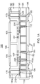
- Figure 1A illustrates a metal-post-enhanced bottom package 100 including a semiconductor or glass interposer 115.
- interposer 115 may comprise a laminated organic interposer.
- interposer 115 may instead comprise a substrate that supports only a single die 105.
- the substrate for bottom package single-die embodiments may comprise glass, semiconductor, or laminated organic polymers.
- Each die 105 electrically couples through a plurality of interconnects such as solder bumps 107 to a corresponding plurality of die interconnects 110 on substrate 115.
- Die interconnects 110 also electrically couple to a die-side redistribution layer that in turn electrically couples to a plurality of metal posts 160.
- the die-side redistribution layer comprises an upper or first die-side RDL 140 and a lower or second die-side RDL 205.
- Alternative embodiments may have just a single metal layer for the die-side redistribution layer or may have more than two metal layers.
- interconnects 110 electrically couple to lower die-side RDL 205.
- die interconnects 110 may be deemed to comprise a means for electrically coupling dies 105 to a die-side redistribution layer such as lower die-side RDL 205.
- Die interconnects 110 and metal posts 160 may comprise any suitable plated metal such as copper or nickel.
- the various redistribution layers disclosed herein such as upper and lower die-side redistribution layers 140 and 205 may comprise copper, nickel, or other conducting metals.
- Upper and lower die-side redistribution layers 140 and 205 form conductors or interconnects within a dielectric layer 130 to electrically couple die interconnects 110 to corresponding ones of metal posts 160.
- a particular die interconnect 110 such as a die interconnect 110a may need to electrically couple to a particular metal post 160 such as a metal post 160a.
- Upper die-side RDL 140 and lower die-side RDL 205 thus electrically couple together these structures.
- upper and lower die-side RDLs 140 and 205 include conductors (not illustrated) to electrically couple die-to-die signals between dies 105.
- lower die-side RDL 205 electrically couple dies 105 to a plurality of through-substrate vias 185.
- Through-substrate vias 185 extend from lower die-side RDL 205 through a core layer 120 of substrate 115 to a board-facing redistribution layer (RDL) 150 that in turn electrically couples to board-facing solder balls 155.
- the composition of core layer 120 depends upon the substrate used in bottom package 100. For example, in a glass interposer embodiment, core layer 120 would comprise glass. Similarly, in a semiconductor interposer embodiment, core layer 120 would comprise semiconductor.
- Board-facing redistribution layer 150 may be insulated from core layer 120 by a dielectric layer 156. For example, dielectric layer 156 may be laminated onto core layer 120 to also line through-substrate vias 185.
- a board-side solder resist or passivation layer 136 includes openings so that exposed pad portions of board-facing redistribution layer 150 may receive solder balls 155. Solder balls 155 electrically couple to a circuit board (not illustrated) or an underlying package.
- a mold compound 165 partially encases dies 105 and metal posts 160. Metal posts 160 may also electrically couple to a top-side redistribution layer 170 on mold compound 165 and dies 105.
- a top-side solder resistor or passivation layer 190 covers top-side redistribution layer 170.
- top-side redistribution layer 170 may be insulated from dies 105 by passivation layer 190, which includes openings to expose pads in top-side redistribution layer 170. These openings may receive interconnects 206 such as solder bumps or copper pillars from a top package 200 as shown in Figure 1B . Upper package 200 is shown in Figure 1B just prior to it being mounted onto bottom package 100.
- Top-side redistribution layer 170 allows for a fan-out between pillars 160 and interconnects 206 from top package 200.
- interposer core 120 would initially be part of a wafer or panel (not illustrated) that would be processed as a whole.
- the panel or wafer would include a plurality of interposer cores 120 that are processed with die interconnects 110 and metal posts 160 prior to dicing interposer cores 120 from the panel or wafer.
- each interposer core 120 may be processed individually after it is diced from a panel or wafer.
- Interposer core 120 may be configured with through-substrate vias 185 in a variety of methods.
- interposer core 120 may be laser drilled and plated to form vias 185.
- a number of blind vias may be for formed using, for example, laser drilling or machining and then plated in interposer core 120 prior to a grinding step that exposes the blind ends of the blind vias and thus forms through-substrate vias 185.
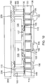
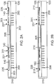
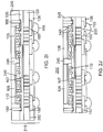
- Figure 2A illustrates a cross-section of an interposer core 120 including a plurality of conductive blind vias 200.
- interposer core 120 is part of a wafer or panel 215 such that a WLP manufacturing technique is being implemented.
- a die-facing surface of interposer core 120 is laser drilled, etched, or mechanically drilled to form a plurality of blind vias that are then plated to form conductive blind vias 200.
- the blind vias Prior to plating, the blind vias may be lined with a dielectric layer (not illustrated) such as dielectric layer 156 shown in Figure 1A .
- a board-facing surface 202 of interposer core 120 has not yet been ground to expose the ends of conductive e blind vias 200 so as to form through-substrate vias 185 discussed with regard to Figures 1A and 1B . Since Figure 2A is illustrating an initial manufacture step, through-substrate vias 185 shown in Figures 1A and 1B are not yet formed.
- a dielectric layer 135 is deposited on a die-facing surface 203 of interposer core 120 supports dielectric layer 135. For example, dielectric layer 135 may be laminated onto die-facing surface 203.
- dielectric layer 135 may comprise polymide, Ajinomoto build-up film, benzocyclobutene-based polymer, or other suitable dielectric materials.
- dielectric layer 135 may be spun onto die-facing surface 203 or deposited using chemical vapor deposition techniques.
- Dielectric layer 135 may be deposited in stages to allow for masking steps so a die-side redistribution layer such as upper die-side redistribution layer 140 may be formed within dielectric layer 135.
- a metal such as copper or nickel may be deposited using plating or electroless techniques to form upper die-side RDL140.
- multiple metal layers may be used in the various redistribution layers disclosed herein.
- dielectric layer 135 may include an additional die-side redistribution layer such as lower die-side RDL 205 formed analogously as discussed with regard to upper die-side RDL 140.
- interposer core 120 may comprise a semiconductor such as silicon that has some conductivity. To prevent shorting to such conductive substrates, lower die-side RDL 205 may be insulated from interposer core 120 by dielectric layer 135 as shown in Figure 2B .
- interposer core 120 comprises a glass or organic material
- lower die-side RDL 205 may contact interposer core 120 as shown in Figure 1A .
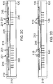
- dielectric layer 135 may be processed such as through etching to form openings for the subsequent formation of metal posts 160 and die interconnects 110 discussed with regard to Figures 1A and 1B .
- dielectric layer 135 may be patterned to include die interconnect openings 201 that expose corresponding portions of lower die-side RDL 205.
- dielectric layer 135 may be patterned to include metal post openings 225 that also expose corresponding portions of upper die-side RDL 140.
- metal seed layer 210 may comprise TiCu, TiW, or copper deposited using, for example, a physical vapor technique. Note that single seed layer 210 lines both die interconnect openings 201 and metal post openings 225.
- a first mask layer 215 such as a wet or dry etch mask layer may then be deposited over seed layer 210 and patterned to re-expose die interconnect openings 201.
- the re-expose may enlarge die interconnect openings 201 as compared to their dimensions in Figure 2A .
- First mask layer 215 is thus deposited in a thickness that matches a desired height for the die interconnects (not yet formed) that will fill die interconnect openings 201.
- die interconnects 110 may then be plated into die interconnect openings 201 as shown in Figure 2D .
- a suitable metal such a copper or nickel may be electroplated to form die interconnects 110.
- First mask layer 215of Figure 2C may then be stripped or removed from panel or wafer 215 at this time.
- Metal posts 160 of Figure 1A and 1B have a greater height or length as compared to die interconnects 110. Thus, in some embodiments metal posts 160 are not plated at the time of plating die interconnects 110 since first mask layer 215 has a height to match a desired height for die interconnects 110 and not for metal posts 160. The formation of metal posts 160 may then begin with a deposition of a second mask layer 220 over seed layer 210 as shown in Figure 2E . As compared to first mask layer 215 ( Figure 2C ), second mask layer 220 has a greater thickness or height so as to accommodate the greater height of metal posts 160 as compared to die interconnects 110. Analogous to first mask layer 215, second mask layer 220 is patterned to re-expose and enlarge metal post openings 225.
- Metal posts 160 may then be plated into metal post openings 225 and second mask layer 220 stripped or otherwise removed as shown in Figure 2F . Similarly, the exposed portions of seed layer 210 are also etched away at this time. However, there will remain those portions of seed layer 210 (not illustrated) onto which die interconnects 110 and metal posts 160 were plated. The etching of seed layer 210 may produce the same amount of undercut (not illustrated) on those portions remaining under die interconnects 110 and metal posts 160.
- interconnects on dies 105 such as solder bumps 107 or copper pillars electrically couple to corresponding die interconnects 110 on panel or wafer 215.
- An underfill 240 may also be applied at this time to assist in securing dies 105 to panel or wafer 215.
- a mold compound 245 may then be applied to at least partially encapsulate dies 105 as shown in Figure 2H . Mold compound also partially encapsulates metal posts 160. An upper surface for both metal posts and dies 105 may be left exposed after application of mold compound 245. Alternatively, a grinding process may be used to expose metal posts 160.
- Through-substrate vias 185 may then exposed on the bottom or board-facing surface of interposer core 120.
- a manufacturer may grind board-facing side 202 of wafer or panel 215 to expose what had been the blind ends of conductive blind vias 200 (shown, for example in Figure 2H ) to form through substrate-vias 185.
- a board-facing redistribution layer 150 may then be deposited on board-facing surface 202 along with a solder resist or passivation layer 136 that is patterned for form openings for solder balls 155 as shown in Figure 2I .
- bottom package 250 its die-facing surface is shown in plan view in Figure 3 .
- Metal posts 160 are arranged on a periphery of bottom package 250 with regard to dies 105. Mold compound 245 fills the spaces between metal posts 160 and dies 105. But such an arrangement need not include the keep-out area between metal posts 160 and dies 105 as in conventional interconnect bar packages.
- the manufacture of an interconnect bar requires a certain keep-out area with regard to its perimeter in that the interconnect bar substrate is typically laser drilled to form vias for the subsequent plating of metal posts. Such drilling cannot be performed too closely to the interconnect bar substrate perimeter.
- metal posts 160 are deposited on the same seed layer 210 on which die interconnects 110 are deposited as discussed with regard to, for example, Figure 2F . Density becomes even worse for conventional bottom packages that use solder balls for the interconnects to the top package. Thus, bottom package 250 has advantageously increased density as compared to conventional approaches. A flowchart summarizing the manufacturing process will now be discussed.
- a step 400 comprises exposing a redistribution layer through a plurality of die interconnect openings and a plurality of metal post openings within a dielectric layer on a substrate surface.
- the formation of die interconnect openings 201 shown in Figure 4C as well as the formation of metal post openings 235 shown in Figure 2E are examples of step 400.
- a step 405 comprises forming die interconnects in the die interconnect openings.
- the formation of die interconnects 110 shown in Figure 2D provides an example of step 405.
- a step 410 comprises forming metal posts in the metal post openings.
- the formation of metal posts 160 shown in Figure 2F provides an example of step 410.
- Integrated circuit packages including a bottom package with metal posts as disclosed herein may be incorporated into a wide variety of electronic systems.
- a cell phone 500, a laptop 505, and a tablet PC 510 may all include an integrated circuit package incorporating a metal-post-containing bottom package constructed in accordance with the disclosure.
- Other exemplary electronic systems such as a music player, a video player, a communication device, and a personal computer may also be configured with integrated circuit packages constructed in accordance with the disclosure.
Landscapes
- Engineering & Computer Science (AREA)
- Microelectronics & Electronic Packaging (AREA)
- Production Of Multi-Layered Print Wiring Board (AREA)
- Structures Or Materials For Encapsulating Or Coating Semiconductor Devices Or Solid State Devices (AREA)
Applications Claiming Priority (3)
| Application Number | Priority Date | Filing Date | Title |
|---|---|---|---|
| US201461941345P | 2014-02-18 | 2014-02-18 | |
| US14/254,494 US10971476B2 (en) | 2014-02-18 | 2014-04-16 | Bottom package with metal post interconnections |
| PCT/US2015/014870 WO2015126638A1 (en) | 2014-02-18 | 2015-02-06 | Bottom package with metal post interconnections |
Publications (2)
| Publication Number | Publication Date |
|---|---|
| EP3108499A1 EP3108499A1 (en) | 2016-12-28 |
| EP3108499B1 true EP3108499B1 (en) | 2021-09-08 |
Family
ID=53798778
Family Applications (1)
| Application Number | Title | Priority Date | Filing Date |
|---|---|---|---|
| EP15704689.7A Active EP3108499B1 (en) | 2014-02-18 | 2015-02-06 | Bottom package with metal post interconnections |
Country Status (5)
| Country | Link |
|---|---|
| US (1) | US10971476B2 (https=) |
| EP (1) | EP3108499B1 (https=) |
| JP (1) | JP2017505999A (https=) |
| CN (1) | CN106030791A (https=) |
| WO (1) | WO2015126638A1 (https=) |
Cited By (1)
| Publication number | Priority date | Publication date | Assignee | Title |
|---|---|---|---|---|
| US20220246496A1 (en) * | 2021-02-01 | 2022-08-04 | Qualcomm Incorporated | Package having a substrate comprising surface interconnects aligned with a surface of the substrate |
Families Citing this family (47)
| Publication number | Priority date | Publication date | Assignee | Title |
|---|---|---|---|---|
| US9735129B2 (en) * | 2014-03-21 | 2017-08-15 | Taiwan Semiconductor Manufacturing Company, Ltd. | Semiconductor packages and methods of forming the same |
| US9318452B2 (en) | 2014-03-21 | 2016-04-19 | Taiwan Semiconductor Manufacturing Company, Ltd. | Semiconductor packages and methods of forming the same |
| US9478521B2 (en) | 2014-09-25 | 2016-10-25 | Taiwan Semiconductor Manufacturing Company, Ltd. | Package-on-package Structure |
| US9443799B2 (en) | 2014-12-16 | 2016-09-13 | International Business Machines Corporation | Interposer with lattice construction and embedded conductive metal structures |
| US10515884B2 (en) * | 2015-02-17 | 2019-12-24 | Advanced Semiconductor Engineering, Inc. | Substrate having a conductive structure within photo-sensitive resin |
| KR20160122020A (ko) * | 2015-04-13 | 2016-10-21 | 에스케이하이닉스 주식회사 | 기판 및 이를 구비하는 반도체 패키지 |
| US9437536B1 (en) | 2015-05-08 | 2016-09-06 | Invensas Corporation | Reversed build-up substrate for 2.5D |
| US10211160B2 (en) * | 2015-09-08 | 2019-02-19 | Invensas Corporation | Microelectronic assembly with redistribution structure formed on carrier |
| US10438881B2 (en) * | 2015-10-29 | 2019-10-08 | Marvell World Trade Ltd. | Packaging arrangements including high density interconnect bridge |
| WO2017111952A1 (en) * | 2015-12-22 | 2017-06-29 | Intel Corporation | Ultra small molded module integrated with die by module-on-wafer assembly |
| US10204893B2 (en) | 2016-05-19 | 2019-02-12 | Invensas Bonding Technologies, Inc. | Stacked dies and methods for forming bonded structures |
| US9865566B1 (en) | 2016-06-15 | 2018-01-09 | Taiwan Semiconductor Manufacturing Company Ltd. | Semiconductor structure and manufacturing method thereof |
| US9960328B2 (en) | 2016-09-06 | 2018-05-01 | Amkor Technology, Inc. | Semiconductor device and manufacturing method thereof |
| KR101942727B1 (ko) * | 2016-09-12 | 2019-01-28 | 삼성전기 주식회사 | 팬-아웃 반도체 패키지 |
| US10729000B2 (en) * | 2016-09-28 | 2020-07-28 | Intel Corporation | Thermal conductivity for integrated circuit packaging |
| US10249552B2 (en) * | 2017-02-22 | 2019-04-02 | Jmj Korea Co., Ltd. | Semiconductor package having double-sided heat dissipation structure |
| US10217720B2 (en) | 2017-06-15 | 2019-02-26 | Invensas Corporation | Multi-chip modules formed using wafer-level processing of a reconstitute wafer |
| CN211858622U (zh) | 2017-06-16 | 2020-11-03 | 株式会社村田制作所 | 电路基板及电路模块 |
| US10504854B2 (en) * | 2017-12-07 | 2019-12-10 | Intel Corporation | Through-stiffener inerconnects for package-on-package apparatus and methods of assembling same |
| CN109962152B (zh) * | 2017-12-25 | 2024-06-18 | 成都万应微电子有限公司 | 热电冷却基板及封装方法、集成电路芯片及封装方法 |
| US10468339B2 (en) | 2018-01-19 | 2019-11-05 | Taiwan Semiconductor Manufacturing Company, Ltd. | Heterogeneous fan-out structure and method of manufacture |
| KR102063470B1 (ko) * | 2018-05-03 | 2020-01-09 | 삼성전자주식회사 | 반도체 패키지 |
| US11276676B2 (en) | 2018-05-15 | 2022-03-15 | Invensas Bonding Technologies, Inc. | Stacked devices and methods of fabrication |
| US10910344B2 (en) | 2018-06-22 | 2021-02-02 | Xcelsis Corporation | Systems and methods for releveled bump planes for chiplets |
| WO2020010265A1 (en) | 2018-07-06 | 2020-01-09 | Invensas Bonding Technologies, Inc. | Microelectronic assemblies |
| WO2020010136A1 (en) | 2018-07-06 | 2020-01-09 | Invensas Bonding Technologies, Inc. | Molded direct bonded and interconnected stack |
| CN109216298A (zh) * | 2018-08-10 | 2019-01-15 | 华进半导体封装先导技术研发中心有限公司 | 一种扇出型芯片封装结构及其制造方法 |
| CN109300882A (zh) * | 2018-09-20 | 2019-02-01 | 蔡亲佳 | 堆叠嵌入式封装结构及其制作方法 |
| JP7245037B2 (ja) * | 2018-11-30 | 2023-03-23 | ローム株式会社 | 半導体装置 |
| CN109994438B (zh) * | 2019-03-29 | 2021-04-02 | 上海中航光电子有限公司 | 芯片封装结构及其封装方法 |
| US10930592B2 (en) * | 2019-05-07 | 2021-02-23 | Google Llc | Wafer level fan-out application specific integrated circuit bridge memory stack |
| US11296053B2 (en) | 2019-06-26 | 2022-04-05 | Invensas Bonding Technologies, Inc. | Direct bonded stack structures for increased reliability and improved yield in microelectronics |
| US11171127B2 (en) * | 2019-08-02 | 2021-11-09 | Amkor Technology Singapore Holding Pte. Ltd. | Semiconductor device and method of manufacturing semiconductor device |
| US12388061B2 (en) | 2019-08-02 | 2025-08-12 | Amkor Technology Singapore Holding Pte. Ltd. | Semiconductor device and method of manufacturing semiconductor device |
| US11133263B2 (en) | 2019-09-17 | 2021-09-28 | Intel Corporation | High-density interconnects for integrated circuit packages |
| US11581262B2 (en) * | 2019-10-02 | 2023-02-14 | Qualcomm Incorporated | Package comprising a die and die side redistribution layers (RDL) |
| US11631647B2 (en) | 2020-06-30 | 2023-04-18 | Adeia Semiconductor Bonding Technologies Inc. | Integrated device packages with integrated device die and dummy element |
| US11282756B2 (en) * | 2020-08-17 | 2022-03-22 | Taiwan Semiconductor Manufacturing Company Limited | Organic interposer including stress-resistant bonding structures and methods of forming the same |
| US11764177B2 (en) * | 2020-09-04 | 2023-09-19 | Adeia Semiconductor Bonding Technologies Inc. | Bonded structure with interconnect structure |
| US11728273B2 (en) | 2020-09-04 | 2023-08-15 | Adeia Semiconductor Bonding Technologies Inc. | Bonded structure with interconnect structure |
| US12341116B2 (en) * | 2021-01-06 | 2025-06-24 | Huawei Technologies Co., Ltd. | Chip package structure, preparation method, and electronic device |
| CN113130420B (zh) * | 2021-03-19 | 2024-10-18 | 南通越亚半导体有限公司 | 一种嵌埋封装结构及其制造方法 |
| US12308346B2 (en) * | 2021-06-17 | 2025-05-20 | Taiwan Semiconductor Manufacturing Company, Ltd. | Semiconductor die with tapered sidewall in package |
| TWI825975B (zh) * | 2021-09-10 | 2023-12-11 | 美商愛玻索立克公司 | 已清洗的封裝用基板的製造方法以及已清洗的封裝用基板 |
| US12599010B2 (en) | 2021-09-22 | 2026-04-07 | Intel Corporation | Microelectronic packages with embedded interposers |
| US12165952B2 (en) * | 2022-02-16 | 2024-12-10 | Taiwan Semiconductor Manufacturing Company, Ltd. | Interposer directly bonded to bonding pads on a plurality of dies |
| US20240071938A1 (en) * | 2022-08-31 | 2024-02-29 | Intel Corporation | Cavity-less interconnect component on glass core |
Family Cites Families (21)
| Publication number | Priority date | Publication date | Assignee | Title |
|---|---|---|---|---|
| JP3798620B2 (ja) | 2000-12-04 | 2006-07-19 | 富士通株式会社 | 半導体装置の製造方法 |
| JP4056854B2 (ja) | 2002-11-05 | 2008-03-05 | 新光電気工業株式会社 | 半導体装置の製造方法 |
| JP3975194B2 (ja) | 2003-12-02 | 2007-09-12 | 株式会社フジクラ | パッケージの製造方法 |
| JP4498991B2 (ja) | 2005-07-15 | 2010-07-07 | 新光電気工業株式会社 | 半導体装置及び電子装置 |
| US20080023805A1 (en) | 2006-07-26 | 2008-01-31 | Texas Instruments Incorporated | Array-Processed Stacked Semiconductor Packages |
| JP2008091795A (ja) * | 2006-10-04 | 2008-04-17 | Shinko Electric Ind Co Ltd | 半導体装置および半導体装置の製造方法 |
| US20080136004A1 (en) * | 2006-12-08 | 2008-06-12 | Advanced Chip Engineering Technology Inc. | Multi-chip package structure and method of forming the same |
| FR2932004B1 (fr) | 2008-06-03 | 2011-08-05 | Commissariat Energie Atomique | Dispositif electronique empile et procede de realisation d'un tel dispositif electronique |
| US8587129B2 (en) | 2009-07-31 | 2013-11-19 | Stats Chippac Ltd. | Integrated circuit packaging system with through silicon via base and method of manufacture thereof |
| US20110147908A1 (en) | 2009-12-17 | 2011-06-23 | Peng Sun | Module for Use in a Multi Package Assembly and a Method of Making the Module and the Multi Package Assembly |
| KR20120007839A (ko) | 2010-07-15 | 2012-01-25 | 삼성전자주식회사 | 적층형 반도체 패키지의 제조방법 |
| JP2012079734A (ja) | 2010-09-30 | 2012-04-19 | Teramikros Inc | 半導体装置及び半導体デバイス並びにそれらの製造方法 |
| US20120080787A1 (en) | 2010-10-05 | 2012-04-05 | Qualcomm Incorporated | Electronic Package and Method of Making an Electronic Package |
| KR20120048991A (ko) * | 2010-11-08 | 2012-05-16 | 삼성전자주식회사 | 반도체 장치 및 그 제조 방법 |
| US8941222B2 (en) * | 2010-11-11 | 2015-01-27 | Advanced Semiconductor Engineering Inc. | Wafer level semiconductor package and manufacturing methods thereof |
| US20130181359A1 (en) | 2012-01-13 | 2013-07-18 | TW Semiconductor Manufacturing Company, Ltd. | Methods and Apparatus for Thinner Package on Package Structures |
| US9412689B2 (en) | 2012-01-24 | 2016-08-09 | Taiwan Semiconductor Manufacturing Company, Ltd. | Semiconductor packaging structure and method |
| TWI508249B (zh) | 2012-04-02 | 2015-11-11 | 矽品精密工業股份有限公司 | 封裝件、半導體封裝結構及其製法 |
| JP6038517B2 (ja) | 2012-07-13 | 2016-12-07 | 新光電気工業株式会社 | 配線基板及びその製造方法 |
| US9735087B2 (en) * | 2012-09-20 | 2017-08-15 | Taiwan Semiconductor Manufacturing Company, Ltd. | Wafer level embedded heat spreader |
| US9252065B2 (en) * | 2013-11-22 | 2016-02-02 | Taiwan Semiconductor Manufacturing Co., Ltd. | Mechanisms for forming package structure |
-
2014
- 2014-04-16 US US14/254,494 patent/US10971476B2/en active Active
-
2015
- 2015-02-06 CN CN201580008881.4A patent/CN106030791A/zh active Pending
- 2015-02-06 EP EP15704689.7A patent/EP3108499B1/en active Active
- 2015-02-06 WO PCT/US2015/014870 patent/WO2015126638A1/en not_active Ceased
- 2015-02-06 JP JP2016549269A patent/JP2017505999A/ja active Pending
Cited By (2)
| Publication number | Priority date | Publication date | Assignee | Title |
|---|---|---|---|---|
| US20220246496A1 (en) * | 2021-02-01 | 2022-08-04 | Qualcomm Incorporated | Package having a substrate comprising surface interconnects aligned with a surface of the substrate |
| US11682607B2 (en) * | 2021-02-01 | 2023-06-20 | Qualcomm Incorporated | Package having a substrate comprising surface interconnects aligned with a surface of the substrate |
Also Published As
| Publication number | Publication date |
|---|---|
| EP3108499A1 (en) | 2016-12-28 |
| US10971476B2 (en) | 2021-04-06 |
| US20150235991A1 (en) | 2015-08-20 |
| CN106030791A (zh) | 2016-10-12 |
| WO2015126638A1 (en) | 2015-08-27 |
| JP2017505999A (ja) | 2017-02-23 |
Similar Documents
| Publication | Publication Date | Title |
|---|---|---|
| EP3108499B1 (en) | Bottom package with metal post interconnections | |
| US12211801B2 (en) | Chip package and method of forming the same | |
| US12218020B2 (en) | Semiconductor packages | |
| US11342196B2 (en) | Integrated circuit package pad and methods of forming | |
| US12394754B2 (en) | Device and method for UBM/RDL routing | |
| US8829666B2 (en) | Semiconductor packages and methods of packaging semiconductor devices | |
| US20130037929A1 (en) | Stackable wafer level packages and related methods | |
| US8860079B2 (en) | Semiconductor packages and methods of packaging semiconductor devices | |
| US12238865B2 (en) | Integrated circuit structure | |
| US20240222291A1 (en) | Semiconductor package with redistribution structure and manufacturing method thereof | |
| US8766441B2 (en) | Methods and apparatus for solder on slot connections in package on package structures | |
| SG190487A1 (en) | Semiconductor packages and methods of packaging semiconductor devices | |
| US20200273718A1 (en) | Package structure and manufacturing method thereof |
Legal Events
| Date | Code | Title | Description |
|---|---|---|---|
| PUAI | Public reference made under article 153(3) epc to a published international application that has entered the european phase |
Free format text: ORIGINAL CODE: 0009012 |
|
| STAA | Information on the status of an ep patent application or granted ep patent |
Free format text: STATUS: REQUEST FOR EXAMINATION WAS MADE |
|
| 17P | Request for examination filed |
Effective date: 20160722 |
|
| AK | Designated contracting states |
Kind code of ref document: A1 Designated state(s): AL AT BE BG CH CY CZ DE DK EE ES FI FR GB GR HR HU IE IS IT LI LT LU LV MC MK MT NL NO PL PT RO RS SE SI SK SM TR |
|
| AX | Request for extension of the european patent |
Extension state: BA ME |
|
| DAX | Request for extension of the european patent (deleted) | ||
| STAA | Information on the status of an ep patent application or granted ep patent |
Free format text: STATUS: EXAMINATION IS IN PROGRESS |
|
| PUAG | Search results despatched under rule 164(2) epc together with communication from examining division |
Free format text: ORIGINAL CODE: 0009017 |
|
| 17Q | First examination report despatched |
Effective date: 20190801 |
|
| B565 | Issuance of search results under rule 164(2) epc |
Effective date: 20190801 |
|
| RIC1 | Information provided on ipc code assigned before grant |
Ipc: H01L 25/10 20060101ALI20190729BHEP Ipc: H01L 23/31 20060101ALI20190729BHEP Ipc: H01L 23/538 20060101ALI20190729BHEP Ipc: H01L 25/065 20060101ALI20190729BHEP Ipc: H01L 23/15 20060101ALN20190729BHEP Ipc: H05K 1/11 20060101ALI20190729BHEP Ipc: H01L 23/522 20060101ALI20190729BHEP Ipc: H01L 23/498 20060101ALI20190729BHEP Ipc: H01L 23/14 20060101ALN20190729BHEP Ipc: H05K 1/09 20060101ALI20190729BHEP Ipc: H01L 23/00 20060101ALI20190729BHEP Ipc: H01L 21/48 20060101AFI20190729BHEP |
|
| GRAP | Despatch of communication of intention to grant a patent |
Free format text: ORIGINAL CODE: EPIDOSNIGR1 |
|
| STAA | Information on the status of an ep patent application or granted ep patent |
Free format text: STATUS: GRANT OF PATENT IS INTENDED |
|
| INTG | Intention to grant announced |
Effective date: 20201030 |
|
| GRAJ | Information related to disapproval of communication of intention to grant by the applicant or resumption of examination proceedings by the epo deleted |
Free format text: ORIGINAL CODE: EPIDOSDIGR1 |
|
| STAA | Information on the status of an ep patent application or granted ep patent |
Free format text: STATUS: EXAMINATION IS IN PROGRESS |
|
| INTC | Intention to grant announced (deleted) | ||
| GRAP | Despatch of communication of intention to grant a patent |
Free format text: ORIGINAL CODE: EPIDOSNIGR1 |
|
| STAA | Information on the status of an ep patent application or granted ep patent |
Free format text: STATUS: GRANT OF PATENT IS INTENDED |
|
| INTG | Intention to grant announced |
Effective date: 20210408 |
|
| GRAS | Grant fee paid |
Free format text: ORIGINAL CODE: EPIDOSNIGR3 |
|
| GRAA | (expected) grant |
Free format text: ORIGINAL CODE: 0009210 |
|
| STAA | Information on the status of an ep patent application or granted ep patent |
Free format text: STATUS: THE PATENT HAS BEEN GRANTED |
|
| AK | Designated contracting states |
Kind code of ref document: B1 Designated state(s): AL AT BE BG CH CY CZ DE DK EE ES FI FR GB GR HR HU IE IS IT LI LT LU LV MC MK MT NL NO PL PT RO RS SE SI SK SM TR |
|
| REG | Reference to a national code |
Ref country code: GB Ref legal event code: FG4D |
|
| REG | Reference to a national code |
Ref country code: AT Ref legal event code: REF Ref document number: 1429337 Country of ref document: AT Kind code of ref document: T Effective date: 20210915 Ref country code: CH Ref legal event code: EP |
|
| REG | Reference to a national code |
Ref country code: IE Ref legal event code: FG4D |
|
| REG | Reference to a national code |
Ref country code: DE Ref legal event code: R096 Ref document number: 602015073062 Country of ref document: DE |
|
| REG | Reference to a national code |
Ref country code: LT Ref legal event code: MG9D |
|
| REG | Reference to a national code |
Ref country code: NL Ref legal event code: MP Effective date: 20210908 |
|
| PG25 | Lapsed in a contracting state [announced via postgrant information from national office to epo] |
Ref country code: HR Free format text: LAPSE BECAUSE OF FAILURE TO SUBMIT A TRANSLATION OF THE DESCRIPTION OR TO PAY THE FEE WITHIN THE PRESCRIBED TIME-LIMIT Effective date: 20210908 Ref country code: RS Free format text: LAPSE BECAUSE OF FAILURE TO SUBMIT A TRANSLATION OF THE DESCRIPTION OR TO PAY THE FEE WITHIN THE PRESCRIBED TIME-LIMIT Effective date: 20210908 Ref country code: SE Free format text: LAPSE BECAUSE OF FAILURE TO SUBMIT A TRANSLATION OF THE DESCRIPTION OR TO PAY THE FEE WITHIN THE PRESCRIBED TIME-LIMIT Effective date: 20210908 Ref country code: LT Free format text: LAPSE BECAUSE OF FAILURE TO SUBMIT A TRANSLATION OF THE DESCRIPTION OR TO PAY THE FEE WITHIN THE PRESCRIBED TIME-LIMIT Effective date: 20210908 Ref country code: BG Free format text: LAPSE BECAUSE OF FAILURE TO SUBMIT A TRANSLATION OF THE DESCRIPTION OR TO PAY THE FEE WITHIN THE PRESCRIBED TIME-LIMIT Effective date: 20211208 Ref country code: ES Free format text: LAPSE BECAUSE OF FAILURE TO SUBMIT A TRANSLATION OF THE DESCRIPTION OR TO PAY THE FEE WITHIN THE PRESCRIBED TIME-LIMIT Effective date: 20210908 Ref country code: FI Free format text: LAPSE BECAUSE OF FAILURE TO SUBMIT A TRANSLATION OF THE DESCRIPTION OR TO PAY THE FEE WITHIN THE PRESCRIBED TIME-LIMIT Effective date: 20210908 Ref country code: NO Free format text: LAPSE BECAUSE OF FAILURE TO SUBMIT A TRANSLATION OF THE DESCRIPTION OR TO PAY THE FEE WITHIN THE PRESCRIBED TIME-LIMIT Effective date: 20211208 |
|
| REG | Reference to a national code |
Ref country code: AT Ref legal event code: MK05 Ref document number: 1429337 Country of ref document: AT Kind code of ref document: T Effective date: 20210908 |
|
| PG25 | Lapsed in a contracting state [announced via postgrant information from national office to epo] |
Ref country code: LV Free format text: LAPSE BECAUSE OF FAILURE TO SUBMIT A TRANSLATION OF THE DESCRIPTION OR TO PAY THE FEE WITHIN THE PRESCRIBED TIME-LIMIT Effective date: 20210908 Ref country code: GR Free format text: LAPSE BECAUSE OF FAILURE TO SUBMIT A TRANSLATION OF THE DESCRIPTION OR TO PAY THE FEE WITHIN THE PRESCRIBED TIME-LIMIT Effective date: 20211209 |
|
| PG25 | Lapsed in a contracting state [announced via postgrant information from national office to epo] |
Ref country code: AT Free format text: LAPSE BECAUSE OF FAILURE TO SUBMIT A TRANSLATION OF THE DESCRIPTION OR TO PAY THE FEE WITHIN THE PRESCRIBED TIME-LIMIT Effective date: 20210908 |
|
| PG25 | Lapsed in a contracting state [announced via postgrant information from national office to epo] |
Ref country code: IS Free format text: LAPSE BECAUSE OF FAILURE TO SUBMIT A TRANSLATION OF THE DESCRIPTION OR TO PAY THE FEE WITHIN THE PRESCRIBED TIME-LIMIT Effective date: 20220108 Ref country code: SM Free format text: LAPSE BECAUSE OF FAILURE TO SUBMIT A TRANSLATION OF THE DESCRIPTION OR TO PAY THE FEE WITHIN THE PRESCRIBED TIME-LIMIT Effective date: 20210908 Ref country code: SK Free format text: LAPSE BECAUSE OF FAILURE TO SUBMIT A TRANSLATION OF THE DESCRIPTION OR TO PAY THE FEE WITHIN THE PRESCRIBED TIME-LIMIT Effective date: 20210908 Ref country code: RO Free format text: LAPSE BECAUSE OF FAILURE TO SUBMIT A TRANSLATION OF THE DESCRIPTION OR TO PAY THE FEE WITHIN THE PRESCRIBED TIME-LIMIT Effective date: 20210908 Ref country code: PT Free format text: LAPSE BECAUSE OF FAILURE TO SUBMIT A TRANSLATION OF THE DESCRIPTION OR TO PAY THE FEE WITHIN THE PRESCRIBED TIME-LIMIT Effective date: 20220110 Ref country code: PL Free format text: LAPSE BECAUSE OF FAILURE TO SUBMIT A TRANSLATION OF THE DESCRIPTION OR TO PAY THE FEE WITHIN THE PRESCRIBED TIME-LIMIT Effective date: 20210908 Ref country code: NL Free format text: LAPSE BECAUSE OF FAILURE TO SUBMIT A TRANSLATION OF THE DESCRIPTION OR TO PAY THE FEE WITHIN THE PRESCRIBED TIME-LIMIT Effective date: 20210908 Ref country code: EE Free format text: LAPSE BECAUSE OF FAILURE TO SUBMIT A TRANSLATION OF THE DESCRIPTION OR TO PAY THE FEE WITHIN THE PRESCRIBED TIME-LIMIT Effective date: 20210908 Ref country code: CZ Free format text: LAPSE BECAUSE OF FAILURE TO SUBMIT A TRANSLATION OF THE DESCRIPTION OR TO PAY THE FEE WITHIN THE PRESCRIBED TIME-LIMIT Effective date: 20210908 Ref country code: AL Free format text: LAPSE BECAUSE OF FAILURE TO SUBMIT A TRANSLATION OF THE DESCRIPTION OR TO PAY THE FEE WITHIN THE PRESCRIBED TIME-LIMIT Effective date: 20210908 |
|
| REG | Reference to a national code |
Ref country code: DE Ref legal event code: R097 Ref document number: 602015073062 Country of ref document: DE |
|
| PLBE | No opposition filed within time limit |
Free format text: ORIGINAL CODE: 0009261 |
|
| STAA | Information on the status of an ep patent application or granted ep patent |
Free format text: STATUS: NO OPPOSITION FILED WITHIN TIME LIMIT |
|
| PG25 | Lapsed in a contracting state [announced via postgrant information from national office to epo] |
Ref country code: DK Free format text: LAPSE BECAUSE OF FAILURE TO SUBMIT A TRANSLATION OF THE DESCRIPTION OR TO PAY THE FEE WITHIN THE PRESCRIBED TIME-LIMIT Effective date: 20210908 |
|
| 26N | No opposition filed |
Effective date: 20220609 |
|
| PG25 | Lapsed in a contracting state [announced via postgrant information from national office to epo] |
Ref country code: SI Free format text: LAPSE BECAUSE OF FAILURE TO SUBMIT A TRANSLATION OF THE DESCRIPTION OR TO PAY THE FEE WITHIN THE PRESCRIBED TIME-LIMIT Effective date: 20210908 |
|
| PG25 | Lapsed in a contracting state [announced via postgrant information from national office to epo] |
Ref country code: MC Free format text: LAPSE BECAUSE OF FAILURE TO SUBMIT A TRANSLATION OF THE DESCRIPTION OR TO PAY THE FEE WITHIN THE PRESCRIBED TIME-LIMIT Effective date: 20210908 |
|
| REG | Reference to a national code |
Ref country code: CH Ref legal event code: PL |
|
| REG | Reference to a national code |
Ref country code: BE Ref legal event code: MM Effective date: 20220228 |
|
| PG25 | Lapsed in a contracting state [announced via postgrant information from national office to epo] |
Ref country code: LU Free format text: LAPSE BECAUSE OF NON-PAYMENT OF DUE FEES Effective date: 20220206 |
|
| PG25 | Lapsed in a contracting state [announced via postgrant information from national office to epo] |
Ref country code: LI Free format text: LAPSE BECAUSE OF NON-PAYMENT OF DUE FEES Effective date: 20220228 Ref country code: IT Free format text: LAPSE BECAUSE OF FAILURE TO SUBMIT A TRANSLATION OF THE DESCRIPTION OR TO PAY THE FEE WITHIN THE PRESCRIBED TIME-LIMIT Effective date: 20210908 Ref country code: IE Free format text: LAPSE BECAUSE OF NON-PAYMENT OF DUE FEES Effective date: 20220206 Ref country code: CH Free format text: LAPSE BECAUSE OF NON-PAYMENT OF DUE FEES Effective date: 20220228 |
|
| PG25 | Lapsed in a contracting state [announced via postgrant information from national office to epo] |
Ref country code: BE Free format text: LAPSE BECAUSE OF NON-PAYMENT OF DUE FEES Effective date: 20220228 |
|
| PG25 | Lapsed in a contracting state [announced via postgrant information from national office to epo] |
Ref country code: HU Free format text: LAPSE BECAUSE OF FAILURE TO SUBMIT A TRANSLATION OF THE DESCRIPTION OR TO PAY THE FEE WITHIN THE PRESCRIBED TIME-LIMIT; INVALID AB INITIO Effective date: 20150206 |
|
| PG25 | Lapsed in a contracting state [announced via postgrant information from national office to epo] |
Ref country code: MK Free format text: LAPSE BECAUSE OF FAILURE TO SUBMIT A TRANSLATION OF THE DESCRIPTION OR TO PAY THE FEE WITHIN THE PRESCRIBED TIME-LIMIT Effective date: 20210908 Ref country code: CY Free format text: LAPSE BECAUSE OF FAILURE TO SUBMIT A TRANSLATION OF THE DESCRIPTION OR TO PAY THE FEE WITHIN THE PRESCRIBED TIME-LIMIT Effective date: 20210908 |
|
| PG25 | Lapsed in a contracting state [announced via postgrant information from national office to epo] |
Ref country code: MT Free format text: LAPSE BECAUSE OF FAILURE TO SUBMIT A TRANSLATION OF THE DESCRIPTION OR TO PAY THE FEE WITHIN THE PRESCRIBED TIME-LIMIT Effective date: 20210908 |
|
| REG | Reference to a national code |
Ref country code: DE Ref legal event code: R079 Ref document number: 602015073062 Country of ref document: DE Free format text: PREVIOUS MAIN CLASS: H01L0021480000 Ipc: H10W0076010000 |
|
| PG25 | Lapsed in a contracting state [announced via postgrant information from national office to epo] |
Ref country code: TR Free format text: LAPSE BECAUSE OF FAILURE TO SUBMIT A TRANSLATION OF THE DESCRIPTION OR TO PAY THE FEE WITHIN THE PRESCRIBED TIME-LIMIT Effective date: 20210908 |
|
| PGFP | Annual fee paid to national office [announced via postgrant information from national office to epo] |
Ref country code: GB Payment date: 20260113 Year of fee payment: 12 |
|
| PGFP | Annual fee paid to national office [announced via postgrant information from national office to epo] |
Ref country code: DE Payment date: 20260115 Year of fee payment: 12 |
|
| PGFP | Annual fee paid to national office [announced via postgrant information from national office to epo] |
Ref country code: FR Payment date: 20260109 Year of fee payment: 12 |