EP3105773B1 - An electron emitter for an x-ray tube - Google Patents
An electron emitter for an x-ray tube Download PDFInfo
- Publication number
- EP3105773B1 EP3105773B1 EP15705247.3A EP15705247A EP3105773B1 EP 3105773 B1 EP3105773 B1 EP 3105773B1 EP 15705247 A EP15705247 A EP 15705247A EP 3105773 B1 EP3105773 B1 EP 3105773B1
- Authority
- EP
- European Patent Office
- Prior art keywords
- electron
- electron emitter
- emission
- ray
- emitter
- Prior art date
- Legal status (The legal status is an assumption and is not a legal conclusion. Google has not performed a legal analysis and makes no representation as to the accuracy of the status listed.)
- Active
Links
- 239000002086 nanomaterial Substances 0.000 claims description 30
- 239000000463 material Substances 0.000 claims description 28
- 238000010438 heat treatment Methods 0.000 claims description 24
- 239000000758 substrate Substances 0.000 claims description 24
- 125000006850 spacer group Chemical group 0.000 claims description 7
- VYPSYNLAJGMNEJ-UHFFFAOYSA-N Silicium dioxide Chemical group O=[Si]=O VYPSYNLAJGMNEJ-UHFFFAOYSA-N 0.000 claims description 6
- 229910052681 coesite Inorganic materials 0.000 claims description 3
- 229910052906 cristobalite Inorganic materials 0.000 claims description 3
- 239000000377 silicon dioxide Substances 0.000 claims description 3
- 239000007787 solid Substances 0.000 claims description 3
- 229910052682 stishovite Inorganic materials 0.000 claims description 3
- 229910052905 tridymite Inorganic materials 0.000 claims description 3
- 235000012239 silicon dioxide Nutrition 0.000 claims description 2
- 239000011248 coating agent Substances 0.000 description 19
- 238000000576 coating method Methods 0.000 description 19
- 230000008901 benefit Effects 0.000 description 17
- 238000000034 method Methods 0.000 description 15
- PXHVJJICTQNCMI-UHFFFAOYSA-N Nickel Chemical compound [Ni] PXHVJJICTQNCMI-UHFFFAOYSA-N 0.000 description 14
- 230000008569 process Effects 0.000 description 10
- XEEYBQQBJWHFJM-UHFFFAOYSA-N Iron Chemical compound [Fe] XEEYBQQBJWHFJM-UHFFFAOYSA-N 0.000 description 8
- 238000010894 electron beam technology Methods 0.000 description 8
- 229910052759 nickel Inorganic materials 0.000 description 8
- 229910045601 alloy Inorganic materials 0.000 description 7
- 239000000956 alloy Substances 0.000 description 7
- 239000002041 carbon nanotube Substances 0.000 description 7
- OKTJSMMVPCPJKN-UHFFFAOYSA-N Carbon Chemical compound [C] OKTJSMMVPCPJKN-UHFFFAOYSA-N 0.000 description 6
- 238000001179 sorption measurement Methods 0.000 description 6
- 229910021393 carbon nanotube Inorganic materials 0.000 description 5
- 239000004020 conductor Substances 0.000 description 5
- 230000005684 electric field Effects 0.000 description 5
- 239000007789 gas Substances 0.000 description 5
- 231100000572 poisoning Toxicity 0.000 description 5
- 230000000607 poisoning effect Effects 0.000 description 5
- 229910052721 tungsten Inorganic materials 0.000 description 5
- 238000002591 computed tomography Methods 0.000 description 4
- 238000005516 engineering process Methods 0.000 description 4
- 229910052742 iron Inorganic materials 0.000 description 4
- 230000007246 mechanism Effects 0.000 description 4
- 229910001220 stainless steel Inorganic materials 0.000 description 4
- 239000010935 stainless steel Substances 0.000 description 4
- 230000004913 activation Effects 0.000 description 3
- 238000001816 cooling Methods 0.000 description 3
- 230000000694 effects Effects 0.000 description 3
- 230000001976 improved effect Effects 0.000 description 3
- 238000004519 manufacturing process Methods 0.000 description 3
- 238000002844 melting Methods 0.000 description 3
- 230000008018 melting Effects 0.000 description 3
- 238000012986 modification Methods 0.000 description 3
- 230000004048 modification Effects 0.000 description 3
- 239000000126 substance Substances 0.000 description 3
- WFKWXMTUELFFGS-UHFFFAOYSA-N tungsten Chemical compound [W] WFKWXMTUELFFGS-UHFFFAOYSA-N 0.000 description 3
- 239000010937 tungsten Substances 0.000 description 3
- 239000000919 ceramic Substances 0.000 description 2
- 238000005229 chemical vapour deposition Methods 0.000 description 2
- 239000002019 doping agent Substances 0.000 description 2
- 239000011521 glass Substances 0.000 description 2
- 238000003384 imaging method Methods 0.000 description 2
- 230000006872 improvement Effects 0.000 description 2
- 229910052750 molybdenum Inorganic materials 0.000 description 2
- 150000004767 nitrides Chemical class 0.000 description 2
- 238000009659 non-destructive testing Methods 0.000 description 2
- 230000000737 periodic effect Effects 0.000 description 2
- 230000008929 regeneration Effects 0.000 description 2
- 238000011069 regeneration method Methods 0.000 description 2
- 229910021332 silicide Inorganic materials 0.000 description 2
- 241000894007 species Species 0.000 description 2
- 229910052717 sulfur Inorganic materials 0.000 description 2
- 229910052715 tantalum Inorganic materials 0.000 description 2
- 150000004772 tellurides Chemical class 0.000 description 2
- 238000004846 x-ray emission Methods 0.000 description 2
- 241001455273 Tetrapoda Species 0.000 description 1
- 230000003213 activating effect Effects 0.000 description 1
- QVGXLLKOCUKJST-UHFFFAOYSA-N atomic oxygen Chemical compound [O] QVGXLLKOCUKJST-UHFFFAOYSA-N 0.000 description 1
- 229910052799 carbon Inorganic materials 0.000 description 1
- 239000010406 cathode material Substances 0.000 description 1
- 229910052729 chemical element Inorganic materials 0.000 description 1
- 238000000701 chemical imaging Methods 0.000 description 1
- 239000013626 chemical specie Substances 0.000 description 1
- 238000004590 computer program Methods 0.000 description 1
- 230000003247 decreasing effect Effects 0.000 description 1
- 238000002059 diagnostic imaging Methods 0.000 description 1
- 230000009977 dual effect Effects 0.000 description 1
- 230000008030 elimination Effects 0.000 description 1
- 238000003379 elimination reaction Methods 0.000 description 1
- 238000000605 extraction Methods 0.000 description 1
- 230000001939 inductive effect Effects 0.000 description 1
- 238000007689 inspection Methods 0.000 description 1
- 238000009607 mammography Methods 0.000 description 1
- 229910052751 metal Inorganic materials 0.000 description 1
- 239000002184 metal Substances 0.000 description 1
- 238000012544 monitoring process Methods 0.000 description 1
- 239000002105 nanoparticle Substances 0.000 description 1
- 239000002073 nanorod Substances 0.000 description 1
- 239000002071 nanotube Substances 0.000 description 1
- 239000002070 nanowire Substances 0.000 description 1
- 230000003287 optical effect Effects 0.000 description 1
- 229910052760 oxygen Inorganic materials 0.000 description 1
- 239000001301 oxygen Substances 0.000 description 1
- 238000012545 processing Methods 0.000 description 1
- 239000003870 refractory metal Substances 0.000 description 1
- 230000000630 rising effect Effects 0.000 description 1
- 239000004065 semiconductor Substances 0.000 description 1
- 238000007493 shaping process Methods 0.000 description 1
- 230000000087 stabilizing effect Effects 0.000 description 1
- 230000002123 temporal effect Effects 0.000 description 1
Images


Classifications
-
- H—ELECTRICITY
- H01—ELECTRIC ELEMENTS
- H01J—ELECTRIC DISCHARGE TUBES OR DISCHARGE LAMPS
- H01J35/00—X-ray tubes
- H01J35/02—Details
- H01J35/04—Electrodes ; Mutual position thereof; Constructional adaptations therefor
- H01J35/06—Cathodes
- H01J35/065—Field emission, photo emission or secondary emission cathodes
-
- H—ELECTRICITY
- H01—ELECTRIC ELEMENTS
- H01J—ELECTRIC DISCHARGE TUBES OR DISCHARGE LAMPS
- H01J35/00—X-ray tubes
- H01J35/02—Details
- H01J35/04—Electrodes ; Mutual position thereof; Constructional adaptations therefor
- H01J35/06—Cathodes
-
- G—PHYSICS
- G01—MEASURING; TESTING
- G01N—INVESTIGATING OR ANALYSING MATERIALS BY DETERMINING THEIR CHEMICAL OR PHYSICAL PROPERTIES
- G01N23/00—Investigating or analysing materials by the use of wave or particle radiation, e.g. X-rays or neutrons, not covered by groups G01N3/00 – G01N17/00, G01N21/00 or G01N22/00
- G01N23/02—Investigating or analysing materials by the use of wave or particle radiation, e.g. X-rays or neutrons, not covered by groups G01N3/00 – G01N17/00, G01N21/00 or G01N22/00 by transmitting the radiation through the material
- G01N23/04—Investigating or analysing materials by the use of wave or particle radiation, e.g. X-rays or neutrons, not covered by groups G01N3/00 – G01N17/00, G01N21/00 or G01N22/00 by transmitting the radiation through the material and forming images of the material
- G01N23/046—Investigating or analysing materials by the use of wave or particle radiation, e.g. X-rays or neutrons, not covered by groups G01N3/00 – G01N17/00, G01N21/00 or G01N22/00 by transmitting the radiation through the material and forming images of the material using tomography, e.g. computed tomography [CT]
-
- G—PHYSICS
- G01—MEASURING; TESTING
- G01V—GEOPHYSICS; GRAVITATIONAL MEASUREMENTS; DETECTING MASSES OR OBJECTS; TAGS
- G01V5/00—Prospecting or detecting by the use of ionising radiation, e.g. of natural or induced radioactivity
-
- H—ELECTRICITY
- H01—ELECTRIC ELEMENTS
- H01J—ELECTRIC DISCHARGE TUBES OR DISCHARGE LAMPS
- H01J2201/00—Electrodes common to discharge tubes
- H01J2201/30—Cold cathodes
- H01J2201/304—Field emission cathodes
- H01J2201/30446—Field emission cathodes characterised by the emitter material
- H01J2201/30488—Nitrides
-
- H—ELECTRICITY
- H01—ELECTRIC ELEMENTS
- H01J—ELECTRIC DISCHARGE TUBES OR DISCHARGE LAMPS
- H01J2201/00—Electrodes common to discharge tubes
- H01J2201/30—Cold cathodes
- H01J2201/304—Field emission cathodes
- H01J2201/30446—Field emission cathodes characterised by the emitter material
- H01J2201/30496—Oxides
Definitions
- Example embodiments presented herein are directed towards an electron emitter for an x-ray tube.
- the electron emitter comprises a nanostructure coating made of oxides, nitrides, silicides, selinides or tellurides.
- Example embodiments are further directed towards an x-ray tube.
- the emission of electrons from the surface of a conductor is caused by heating the conductor to elevated temperatures, the thermionic emission; by shaping the conductor into a sharp point and applying a negative voltage, the field emission, or by applying a moderate heating to assist the field emission, for example, Schottky emission (as a matter of fact, there are more emission mechanisms as well, like photoemission and gas ion impact emission).
- An electron emitter is commonly referred to as a cathode.
- the cathode working under the respective emission modes are called the hot cathode, cold cathode or Schottky cathode, respectively.
- a device that provides electron beams is called an electron source or electron gun. The electrons are perhaps the most common stimulus for secondary beams.
- an x-ray source is a device comprising 1) a cathode and 2) an electron receiver known as the target or anode.
- the anode is the x-ray emitter.
- the cathode and the anode are arranged in a particular configuration, and are enclosed in a vacuum housing.
- an x-ray system may comprise the following components, 1) the x-ray source, 2) the computerized manipulation and handling device, 3) the detectors and 4) the power unit(s).
- x-ray finds applications in medical imaging, security inspection, and nondestructive testing in industry.
- CNTs carbon nanotubes
- At least one object of the example embodiments presented herein is to provide an alternative electron emitter, which may provide for alternate means of electron emission to overcome the material and operational disadvantages inherent in the hot cathodes as well as in the cold cathode based on CNTs; and at the same time brings in improved performance of the x-ray sources.
- the example embodiments presented herein are directed towards an electron emitter for x-ray device.
- the electron emitter comprises a nanostructure material made of ZnO.
- Such a nanostructure material makes the electron emitter suitable for field emission and more importantly for Schottky emission.
- the use of a thermally assisted electron emission allows for compensation in the properties of the hot and cold cathodes.
- the benefit of the example embodiments will be clear, when the comparisons are made between the Schottky emission, the thermionic emission, and the field emission. It is well known that a cold cathode can be poisoned by the adsorption of electronegative elements such as S, Cl existing as residual gaseous species in the tube. If the adsorption is severe, the cathode will cease to emit electrons.
- the cold cathode can be regenerated by removing the tube from the housing and baking out the entire tube in an oven, and then mount the tube back to see the effect of baking out, a cumbersome process.
- the heating resulting in a moderate temperature rise at the cathode assists the emission of the electrons while at the same time preventing the adsorption of the poisoning gas atoms or molecules on the cathode.
- the regeneration can be done by heating the cathode directly without removing the tube from the tube housing.
- the lower power consumption will result in a more compact power source to be utilized, thereby allowing for the x-ray device to become more portable.
- the use of such electron emission mode eliminates the need for a cooling system or long cool down and warm up periods which are common for hot filament-based systems.
- the example embodiments are directed towards an electron emitter for an x-ray tube.
- the electron emitter comprises an electrically conductive substrate and a nanostructure material.
- the nanostructure material is comprised on at least a portion of the electrically conductive substrate.
- the nanostructure material is made of ZnO.
- An example advantage of the above embodiment is that the use of such a nanostructure material allows for a thermally assisted emission, such as a Schottky emission. Thus, a more compact x-ray device may be obtained as compared with Thermionic emission.
- the electrically conductive substrate is made of stainless steel, nickel, nickel based alloys, iron or iron based alloys.
- the electrically conductive substrate is in the shape of a solid cylinder with a circular, polygonal, or star cross-section.
- An example advantage of the above embodiment is the ability to control the direction, density, as well as other characteristics, of the electron emission by varying the shape of the electron emitter.
- the nanostructure material is doped or co-doped with a dopant element comprised in column IA, IIA, IB, IIIA, VIA, or VIIA in periodic table of the elements.
- An example advantage of such embodiments is the ability of providing an alternative to the CNT based electron emitters.
- the use of such an alternative provides an example benefit of providing an electron emitter which is more compatible with Schottky based emission.
- Carbon based electron emitters are prone to damage at the temperatures and reactive gaseous environment of typical tube manufacture process. Whereas ZnO and related materials are high in melting temperature and chemically more stable with equally attractive field emission performance to CNTs.
- the portions of the electrically conductive substrate which do not comprise the nanostructure material further comprising a dielectric layer.
- the dielectric layer is SiO2.
- the controlling may be in the form of controlling a direction or density of the electron emission.
- the electrically conductive substrate is attachable to a heating element.
- An example advantage of such an embodiment is the ability of providing different electron emission modes, for example, a Schottky emission.
- the electron emitter is configured for Schottky emission when the heating element is in an on-state and the electron emitter is negatively biased. According to some of the example embodiments, the electron emitter is configured for field emission when the heating element is in an off-state and the electron emitter is negatively biased.
- an example advantage of such embodiments is that the electron emitter may be configured for dual operational modes allowing for both field emission and Schottky based emission. Furthermore, a hot filament can also be placed. Such an embodiment has the example advantage of providing a versatile device utilizing all three electron emission modes whenever needed, which may generate x-ray images at various resolutions and contrast levels.
- Some of the embodiments are directed towards an x-ray tube comprising the electron emitter described above.
- An example advantage of having such an x-ray tube is the ability of having a versatile device which may operate in a Schottky emission mode. Thus, the device may be portable as described above.
- the x-ray tube further comprises a plurality of electron emitters arranged to emit electrons towards an electron receiving component.
- the plurality of electron emitters is activated individually, simultaneously or sequentially.
- Such embodiments have the example advantage of providing a more versatile device as activating the different electron emitters may provide a difference in the resulting electron emission. Thus, differences in image resolution, etc. may be obtained.
- the electron emitters disclosed above with the anode constitutes a so called diode X-ray tube.
- the electron source can be configured to consist of the cathode as disclosed above and a grid electrode.
- an X-ray source consisting of this type of electron source and an anode is referred to as a triode tube.
- the example embodiments are directed towards an electron source for X-ray tube.
- the electron source comprises a cathode as disclosed above and a grid, which are placed at a fixed interval of distances and fixed by a ceramic spacer.
- the grid is made of electrically conductive wires of equal diameter.
- the wires are made of high melting point, low vapor pressure and electrically conductive materials, such as W, Mo, Ta, Ni, stainless steel, or nickel based alloys.
- the diameter of the wires varies between 30 um and 150 um.
- the opening ratio of the grid varies between 50% and 80%.
- the surface of the wires in the grid is coated with a thin layer or multilayers of material(s) with properties of pronounced secondary electron emission. Alternatively, the coating is a UV emitting material.
- the coating increases the output intensity of the electrons from the source. It is evident, nevertheless better to point out that placing a grid in front of the cathode is a common practice in vacuum tubes and even field emission devices, the present embodiment exhibits clear distinction to prior art in the following aspects: the cathode material, emission mechanism, and an enhancement effect.
- the overall advantages of a this kind of electron source as manifested in a triode X-ray tube are the independency of the electron beam on the anode, and the enhanced current output.
- Example embodiments presented herein are directed towards an electron emitter for an x-ray device, where the electron emitter comprising a nanostructure material made of ZnO. Such an electron emitter is useful for enabling an x-ray device with a Schottky emission operating mode.
- Figure 1 illustrates a traditional x-ray tube.
- the x-ray tube of Figure 1 features an evacuated glass tube 10 comprising a hot filament cathode 12 and an anode 14 made of refractory metal/alloy.
- the surface of the anode 14 faces the cathode 12 at a predetermined inclination angle.
- An electric current provided by a power supply 13, passes through the filament cathode 12 causing an increase in the temperature of the filament 12 to a level that emits an electron beam 16 from this filament.
- the electron beam 16 is then accelerated towards the anode 14 in the electric field. This results in an x-ray beam 18 which is directed out of the device via a window 20.
- the voltage difference between the cathode and the anode determines the energy of the x-ray beam.
- CNTs carbon nanotubes
- At least one object of the example embodiments presented herein is to provide an alternative electron emitter, which may provide for alternate means of electron emission to overcome the material and operational disadvantages inherent in the hot cathode as well as in the cold cathode based on CNTs; and consequently brings in portable x-ray sources with improved performance.
- the example embodiments presented herein are directed towards an electron emitter for x-ray device.
- the electron emitter comprises a nanostructure material made of ZnO.
- Such a nanostructure material makes the electron emitter suitable for field emission and more importantly for Schottky emission.
- the use of a thermally assisted electron emission allows for compensation in the properties of the hot and cold cathodes.
- the benefit of the example embodiments will be clear, when the comparisons are made between the Schottky emission, the thermionic emission, and the field emission. It is well known that a cold cathode can be poisoned by the adsorption of electronegative elements such as S, Cl existing as residual gaseous species in the tube. If the adsorption is severe, the cathode will cease to emit electrons.
- the cold cathode can be regenerated by removing the tube from the housing and baking out the entire tube in an oven, and then mount the tube back to see the effect of baking out, cumbersome process.
- the heating resulting in a moderate temperature rise at the cathode assists the emission of the electrons while at the same time preventing the adsorption of the poisoning gas atoms or molecules on the cathode.
- the regeneration can be done by heating the cathode directly without removing the tube from the tube housing.
- the lower power consumption will result in a more compact power source to be utilized, thereby allowing for the x-ray device to become more portable.
- the use of such electron emission mode eliminates the need for a cooling system or long cool down and warm up periods which are common for hot filament-based systems.
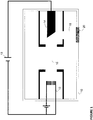
- FIG. 2 illustrates an x-ray device according to the example embodiments.
- the x-ray device of Figure 2 comprises an evacuated glass tube 10 comprising an electron emitter, or cathode, 22 and an electron receiving component 14.
- the surface of the electron receiving component 14 faces the electron emitter 22 at a predetermined inclination angle.
- the plane of the emitters can also be arranged parallel to the electron receiving component.
- An electric current, provided by a power supply 28 passes through a heating element 21 causing an increase in the temperature of the electron emitter 22 to a level that assist the emission of electrons 25 beam from the electron emitter 22, when the cathode at the same time is negatively biased.
- Such emission is known as Schottky emission.
- the emission of Figure 2 is induced by electric field under assistance of a moderate heating.
- the electrons of electron beam 25 are then accelerated towards the electron receiving component 14 with an electric field. This results in an x-ray beam 26 which is directed out of the device via a window 20.
- the voltage difference between the electron emitter and the electron receiving component determines the energy of the x-ray beam.
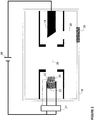
- a grid 30 is placed in between the surface 23 comprising the nanostructures 24 of electron emitter and the electron receiving component 14 that acts as an extraction electrode, as illustrated in Figure 3 .
- a spacer 31 is placed between the electron emitter and the grid 30.
- the grid may be placed at an interval distance between 100um and 1000um which is fixed via the spacer.
- a circular cover is placed on top of the grid acting as the grid electrode providing a voltage to the grid, 32.
- the spacer may be a ceramic spacer.
- the grid is made of electrically conductive wires of equal diameter.
- the wires are made of high melting point, low vapor pressure and electrically conductive materials, such as W, Mo, Ta, Ni, stainless steel, or nickel based alloys.
- the diameter of the wires varies between 30 um and 150 um.
- the linear opening ratio of the grid varies between 50% and 80%.
- the surface of the wires in the grid is coated with a thin layer or multilayers of material(s) with properties of pronounced secondary electron emission, such as MgO and related materials.
- the coating is a UV emitting material, such as GaN and related materials.
- the coating increases the output intensity of the electrons from the electron emitter.
- the overall advantages of a this kind of electron emitter as manifested in a triode X-ray tube, as illustrated in Figure 5 are the independency of the electron beam on the anode, and the enhanced current output.
- the field established between the electron emitter and the grid determines the intensity of the electron beam.
- the voltage difference between the electron emitter and the electron receiving component 14 determines the energy of the x-ray beam.
- the grid and spacer of Figure 3 may be applied to an electron emitter according to any of the example embodiments provided herein.
- the electron emitter 22 comprises an electrically conductive substrate 23 comprising of a coating of nanostructures 24.
- the heating element 21 is attachable to the electrically conductive substrate 23 via two electric feed-through at cathode end of the tube.
- the nanostructure coating 24 may be grown on the electrically conductive substrate 23.
- the nanostructure coating may be in the form of nanoparticles, nanowires, nanorods, nano tetrapods or nanotubes.
- the materials of the substrate can be stainless steel, nickel, nickel-based alloys, iron or iron-based alloys. According to some of the example embodiments, the substrate is pre-formed into various shapes.
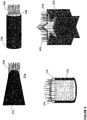
- Figure 4 illustrates example shapes in which the electron emitter may be shaped.
- the electron emitter 22a is in the shape of a rounded pyramid comprising an electrically conductive substrate 23a and a coating of nanostructures 24a.
- a further example of an electron emitter 22b is provided in the form of a solid cylinder also comprising an electrically conductive substrate 23b and a coating of nanostructures 24b.
- Figure 4 provides a further example of an electron emitter in the form of a hollow cylinder 22c featuring an electrically conductive substrate 23c and a coating of nanostructures 24c.
- An additional example of an electron emitter is provided in the form of a hollow star 22d comprising an electrically conductive substrate 23d and a coating of nanostructures 24d. It should be appreciated that such shapes may be adapted for different uses of the x-ray as the shapes may affect the direction of the emitted electrons. It should further be appreciated that other shapes may also be employed in the x-ray device according to the example embodiments.
- the substrates described in Figure 4 may be bundled in parallel at a given space.
- the surface formed by the top ends of the substrates may be planar, concave or convex in shape to shape the focal spot of the electron beam.
- the nanostructure coating may be grown by a solid-liquid-gas phase method, chemical vapour deposition (CVD) process, or a chemical solution method.
- the nanostructure coating is configured to be altered, with respect to morphology, to further facilitate the electron emission by chemical, electrochemical or optical means in or after the growth process.
- the nanostructure coating may be made of oxides, nitrides, silicides, selinides or tellurides.
- the nanostructure coating may be made of ZnO.
- ZnO is an n-type, wide band gap semiconductor. The conductivity is associated with the oxygen vacancy generated in the growth process.
- Improvement on the conductivity is achieved by doping the chemical elements in the columns IA, IIA, IB, IIIA, VIA, VIIA in the periodic table of the elements.
- Post-growth heat treatment is applied to homogenize the dopants or to partially segregate them to the surface.
- the morphology of the nanostructure can be altered by chemical or electrochemical means to achieve local field enhancement.
- UV treatment may also be applied to improve the surface properties.
- a surface coating may be applied to the nanostructures to further enhance the electron emission process through decreasing the work function at the surface of the emitter.
- a dielectric layer for example, SiO 2
- SiO 2 may be added on the electrically conductive substrate in areas in which the coating of the nanostructures is not present. Such a dielectric coating may be useful in directing the electron emission.
- the heating element 21 When a moderate heating is applied, via the heating element 21, while the electron emitter is negatively biased, the electrons are emitted by Schottky emission. When the heating is turned off, while the cathode is negatively biased, the electrons are emitted by field emission.
- the added function of heating which is absent in pre art field emission x-ray sources, may also be applied to regenerate the electron emitter by removing unwanted adsorbed chemical species from the surface of the emitters in the case of cathode poisoning.
- multiple electron emitters may be used in the x-ray device.
- Figure 5 illustrates an x-ray tube in which multiple electron emitters.
- three electron emitters 22_1, 22_2 and 22_3 are assembled in the enclosed tube 10 with the emitters facing the electron receiving component 14.
- the number and spacing of the electron emitters may vary.
- any number of electron emitters may be employed in the x-ray device according to the example embodiments. It should further be appreciated that the electron emitters of Figure 5 may be the electron emitter featured in any of Figures 2 thru 4 , or an emitter of any other shape. It should also be appreciated that the electron emitters need not be identical and may comprise different shapes and/or characteristics with respect to one another.
- the pattern of the arrangement of the electron emitters may be, but is not limited to, linear, circular, rectangle, square, or other polygonal shape.
- the electron emitters 22_1, 22_2 and 22_3 may be arranged so all of them emit electrons 25a-25c directed to one focal spot on the electron receiving component 14, or so that they project a magnified or demagnified image of the emission pattern onto the electron receiving component 14.
- the electron emitters 22_1, 22_2 and 22_3 may be activated collectively or individually, simultaneously or sequentially. Such a flexible activation regime allows a high frequency, pulsing mode for x-ray generation by setting the output frequency of the power source and a wide range of dose selection by choosing the number of activated electron emitters 22_1, 22_2 and 22_3. The activation of the electron emitters 22_1, 22_2 and 22_3 may be controlled by the power supply 28.
- the example embodiments presented herein allow for the individual activation of the electron emitters 22_1, 22_2 and 22_3, thereby providing a mechanism for stabilizing emission current, which is not available in current x-ray systems. It should be appreciated that the inhomogeneity in the emission is a serious problem in large area cathodes or multi cathodes. This problem stems from the geometrical and physical inhomogeneity of the emitters.
- the problem of the emitters described above stems from material and processing issues. Therefore, some of the example embodiments are directed towards an improvement on the growth of the emitter material on the substrate.
- the existence of the inhomogeneity among the emitters is also solved at the component level.
- Such an example embodiment is described by taking a three-cathode configuration as example of Figure 5 .
- Figures 6A and 6B illustrates the current and voltage characteristics of the electron emitter configuration of Figure 4 .
- the plotted points represented by the triangular, square and circular symbols represent the voltages and currents from the electron emitters 22_1, 22_2 and 22_3, respectively, of Figure 5 .
- Figure 6A illustrates an application of voltage V, while keeping a same distance between the same electron emitter and electron receiving component.
- Each electron emitter 22_1, 22_2 and 22_3, will emit current i1, i2 and i3, respectively.
- the amount of current supplied by the electron emission of each electron emitter differs.
- the inhomogeneity may be quantitatively described by formally defining the mean square error or root mean square deviation of the measured current values of all emitters in question, the graphical difference shown in Figure 6A is sufficient to illustrate the point.
- the electrical power source 28 is further configured to supply a potential difference between the at least one electron generating component(s) and the electron receiving component for a diode tube in three bias modes, (-,0: cathode negative, anode grounded), (-,+: cathode negative, anode positive) and (0,+: cathode grounded, anode positive).
- bias modes (-,0: cathode negative, anode grounded), (-,+: cathode negative, anode positive) and (0,+: cathode grounded, anode positive).
- the electrical power source is configured to operate in DC mode, i.e. constant (-, 0), (-, +), (0, +); pulse mode, i.e. square waves with the anode grounded or with the cathode grounded; or AC mode, i.e. a sinus wave.
- DC mode i.e. constant (-, 0), (-, +), (0, +)
- pulse mode i.e. square waves with the anode grounded or with the cathode grounded
- AC mode i.e. a sinus wave.
- An example advantage of providing an electrical power source with different modes of operations is the ability of providing a more versatile device. For example, in pulse and AC modes, a defined rising time, frequency, duty cycle and pulse shape of waveform may be obtained.
- the x-ray device described herein may be used in a number of fields.
- the x-ray device may be used in a security scanning apparatus, for example, as one would find in an airport security check.
- the x-ray device may be easily implemented in such a security system.
- a further example use of the x-ray device discussed herein is in medical scanning devices such as a computed tomography (CT) scanning apparatus or a C-arm type scanning apparatus, which may include a mini C-arm apparatus.
- CT computed tomography
- C-arm type scanning apparatus which may include a mini C-arm apparatus.
- geological surveying apparatus is another example use of the x-ray device described herein.
- the x-ray device described herein may be used in any non-destructive testing apparatus.
- a few example application of the x-ray device may be mammography, veterinary imaging, and X-ray fluorescence spectrometry, etc.
Landscapes
- X-Ray Techniques (AREA)
- Cold Cathode And The Manufacture (AREA)
- Analysing Materials By The Use Of Radiation (AREA)
Applications Claiming Priority (2)
| Application Number | Priority Date | Filing Date | Title |
|---|---|---|---|
| US201461937677P | 2014-02-10 | 2014-02-10 | |
| PCT/EP2015/052789 WO2015118178A1 (en) | 2014-02-10 | 2015-02-10 | An electron emitter for an x-ray tube |
Publications (2)
| Publication Number | Publication Date |
|---|---|
| EP3105773A1 EP3105773A1 (en) | 2016-12-21 |
| EP3105773B1 true EP3105773B1 (en) | 2018-10-10 |
Family
ID=52473906
Family Applications (2)
| Application Number | Title | Priority Date | Filing Date |
|---|---|---|---|
| EP15704775.4A Active EP3105772B1 (en) | 2014-02-10 | 2015-02-10 | An x-ray device |
| EP15705247.3A Active EP3105773B1 (en) | 2014-02-10 | 2015-02-10 | An electron emitter for an x-ray tube |
Family Applications Before (1)
| Application Number | Title | Priority Date | Filing Date |
|---|---|---|---|
| EP15704775.4A Active EP3105772B1 (en) | 2014-02-10 | 2015-02-10 | An x-ray device |
Country Status (12)
| Country | Link |
|---|---|
| US (2) | US10319555B2 (es) |
| EP (2) | EP3105772B1 (es) |
| JP (2) | JP6804304B2 (es) |
| KR (2) | KR102313234B1 (es) |
| CN (2) | CN106463321B (es) |
| AU (2) | AU2015213990B2 (es) |
| BR (2) | BR112016018345B1 (es) |
| CA (2) | CA2939138C (es) |
| MX (2) | MX360238B (es) |
| RU (2) | RU2675791C2 (es) |
| SA (2) | SA516371645B1 (es) |
| WO (2) | WO2015118178A1 (es) |
Families Citing this family (19)
| Publication number | Priority date | Publication date | Assignee | Title |
|---|---|---|---|---|
| US10283311B2 (en) * | 2015-08-21 | 2019-05-07 | Electronics And Telecommunications Research Institute | X-ray source |
| GB2537196B (en) * | 2015-10-02 | 2017-05-10 | Mario Michan Juan | Apparatus and method for electron irradiation scrubbing |
| WO2017092834A1 (en) | 2015-12-04 | 2017-06-08 | Luxbright Ab | An electron guiding and receiving element |
| US10096148B1 (en) | 2017-04-26 | 2018-10-09 | The Aerospace Corporation | Portable x-ray computed tomography |
| TWI651748B (zh) * | 2017-07-10 | 2019-02-21 | 法商歐洲雷射系統與方案解決公司 | 低壓佈線離子電漿放電源,及其用於具有二次發射之電子源的應用 |
| DE102017008810A1 (de) * | 2017-09-20 | 2019-03-21 | Cetteen Gmbh | MBFEX-Röhre |
| CN108072672B (zh) * | 2017-12-14 | 2021-03-02 | 清华大学 | 一种烧蚀结构形貌及产物的在线监测装置及其监测方法 |
| US11955306B2 (en) * | 2018-04-06 | 2024-04-09 | Micro-X Limited | Large scale stable field emitter for high current applications |
| KR102027407B1 (ko) * | 2018-05-16 | 2019-11-04 | 원광대학교산학협력단 | 탄소나노튜브 실을 이용한 필드 에미터 및 냉음극 구조 |
| KR101956153B1 (ko) | 2018-10-04 | 2019-06-24 | 어썸레이 주식회사 | 탄소나노튜브를 포함하는 얀의 제조방법 및 이로부터 제조된 얀 |
| KR101962215B1 (ko) | 2018-11-30 | 2019-03-26 | 어썸레이 주식회사 | 일 방향으로 정렬된 얀을 포함하는 탄소나노튜브 시트를 제조하는 방법 및 이에 의해 제조된 탄소나노튜브 시트 |
| KR101992745B1 (ko) | 2019-01-24 | 2019-06-26 | 어썸레이 주식회사 | 구조적 안정성이 우수하고 전자 방출 효율이 향상된 이미터 및 이를 포함하는 x-선 튜브 |
| US10825634B2 (en) * | 2019-02-21 | 2020-11-03 | Varex Imaging Corporation | X-ray tube emitter |
| US11315751B2 (en) * | 2019-04-25 | 2022-04-26 | The Boeing Company | Electromagnetic X-ray control |
| RU2710455C1 (ru) * | 2019-06-06 | 2019-12-26 | Закрытое акционерное общество "СуперОкс" (ЗАО "СуперОкс") | Многополостной катод для плазменного двигателя |
| KR102099411B1 (ko) * | 2019-07-26 | 2020-04-09 | 어썸레이 주식회사 | 구조적 안정성이 우수한 전계 방출 장치 및 이를 포함하는 x-선 튜브 |
| US11719652B2 (en) | 2020-02-04 | 2023-08-08 | Kla Corporation | Semiconductor metrology and inspection based on an x-ray source with an electron emitter array |
| CN113311012A (zh) * | 2021-05-26 | 2021-08-27 | 西湖大学 | 基于多晶x射线衍射仪的电化学检测装置及其测试方法 |
| RU209775U1 (ru) * | 2021-08-31 | 2022-03-23 | Общество с ограниченной ответственностью "Пространство-время" | Импульсный пьезоэлектрический источник рентгеновского излучения |
Citations (2)
| Publication number | Priority date | Publication date | Assignee | Title |
|---|---|---|---|---|
| EP0905737A1 (en) * | 1997-09-30 | 1999-03-31 | Ise Electronics Corporation | Electron-emitting source and method of manufacturing the same |
| DE102013214096A1 (de) * | 2012-10-04 | 2014-04-10 | Siemens Aktiengesellschaft | Substrat für einen Feldemitter, Verfahren zur Herstellung des Substrates und Verwendung des Substrates |
Family Cites Families (41)
| Publication number | Priority date | Publication date | Assignee | Title |
|---|---|---|---|---|
| US4924485A (en) * | 1987-09-22 | 1990-05-08 | Hoeberling Robert F | Portable radiography system using a relativistic electron beam |
| KR0141174B1 (ko) * | 1994-12-28 | 1998-06-15 | 윤종용 | 초 순간 수상관의 직렬형 음극 신호 개선장치 |
| JPH08250054A (ja) * | 1995-03-14 | 1996-09-27 | Hitachi Ltd | 拡散補給型電子線源およびそれを用いた電子線装置 |
| AU1493799A (en) * | 1997-12-04 | 1999-06-16 | Printable Field Emitters Limited | Field electron emission materials and devices |
| US6277318B1 (en) * | 1999-08-18 | 2001-08-21 | Agere Systems Guardian Corp. | Method for fabrication of patterned carbon nanotube films |
| EP1123558B1 (en) * | 1999-08-20 | 2004-01-21 | Fei Company | Schottky emitter having extended life |
| JP2001250496A (ja) | 2000-03-06 | 2001-09-14 | Rigaku Corp | X線発生装置 |
| US6456691B2 (en) | 2000-03-06 | 2002-09-24 | Rigaku Corporation | X-ray generator |
| US6334939B1 (en) * | 2000-06-15 | 2002-01-01 | The University Of North Carolina At Chapel Hill | Nanostructure-based high energy capacity material |
| US7085351B2 (en) * | 2000-10-06 | 2006-08-01 | University Of North Carolina At Chapel Hill | Method and apparatus for controlling electron beam current |
| US20040240616A1 (en) | 2003-05-30 | 2004-12-02 | Applied Nanotechnologies, Inc. | Devices and methods for producing multiple X-ray beams from multiple locations |
| US6876724B2 (en) * | 2000-10-06 | 2005-04-05 | The University Of North Carolina - Chapel Hill | Large-area individually addressable multi-beam x-ray system and method of forming same |
| US6553096B1 (en) | 2000-10-06 | 2003-04-22 | The University Of North Carolina Chapel Hill | X-ray generating mechanism using electron field emission cathode |
| JP2002238885A (ja) * | 2001-02-02 | 2002-08-27 | Ge Medical Systems Global Technology Co Llc | X線焦点位置制御方法及びそのプログラム並びにx線ct装置及びx線管 |
| JP3810656B2 (ja) * | 2001-07-23 | 2006-08-16 | 株式会社神戸製鋼所 | 微小x線源 |
| US6672925B2 (en) * | 2001-08-17 | 2004-01-06 | Motorola, Inc. | Vacuum microelectronic device and method |
| US6828717B2 (en) * | 2001-10-26 | 2004-12-07 | Matsushita Electric Industrial Co., Ltd. | Electron gun having short length and cathode-ray tube apparatus using such electron gun |
| US7233101B2 (en) * | 2002-12-31 | 2007-06-19 | Samsung Electronics Co., Ltd. | Substrate-supported array having steerable nanowires elements use in electron emitting devices |
| JP2004241295A (ja) * | 2003-02-07 | 2004-08-26 | Hitachi Zosen Corp | カーボンナノチューブを用いた電子放出素子用電極材料およびその製造方法 |
| CN102005358B (zh) * | 2004-05-17 | 2012-09-12 | 迈普尔平版印刷Ip有限公司 | 带电粒子束曝光系统 |
| JP2005332735A (ja) * | 2004-05-21 | 2005-12-02 | Ci Techno:Kk | 電子放出素子及びその製造方法 |
| EP1791186A1 (en) * | 2005-11-25 | 2007-05-30 | Stormled AB | Light emitting diode and method for manufacturing the same |
| US7850941B2 (en) * | 2006-10-20 | 2010-12-14 | General Electric Company | Nanostructure arrays and methods for forming same |
| JP4984234B2 (ja) * | 2007-03-30 | 2012-07-25 | 国立大学法人長岡技術科学大学 | X線発生装置 |
| WO2008124084A2 (en) * | 2007-04-03 | 2008-10-16 | Pinkerton Joseph F | Nanoelectromechanical systems and methods for making the same |
| US7627087B2 (en) | 2007-06-28 | 2009-12-01 | General Electric Company | One-dimensional grid mesh for a high-compression electron gun |
| DE102007034222A1 (de) | 2007-07-23 | 2009-01-29 | Siemens Ag | Röntgenröhre mit einer Feldemissionskathode |
| KR100911434B1 (ko) * | 2007-12-17 | 2009-08-11 | 한국전자통신연구원 | Cnt를 이용한 삼극형 구조의 초소형 x 선관 |
| EP2079095B1 (en) * | 2008-01-11 | 2012-01-11 | UVIS Light AB | Method of manufacturing a field emission display |
| JP5294653B2 (ja) | 2008-02-28 | 2013-09-18 | キヤノン株式会社 | マルチx線発生装置及びx線撮影装置 |
| JP2010186694A (ja) * | 2009-02-13 | 2010-08-26 | Toshiba Corp | X線源、x線発生方法およびx線源製造方法。 |
| EP2411997A1 (en) * | 2009-03-27 | 2012-02-01 | Koninklijke Philips Electronics N.V. | Structured electron emitter for coded source imaging with an x-ray tube |
| JP2011034734A (ja) * | 2009-07-30 | 2011-02-17 | Stanley Electric Co Ltd | 電界放出型電子源 |
| EP2375435B1 (en) * | 2010-04-06 | 2016-07-06 | LightLab Sweden AB | Field emission cathode |
| US20110280371A1 (en) * | 2010-05-12 | 2011-11-17 | Sabee Molloi | TiO2 Nanotube Cathode for X-Ray Generation |
| JP5578612B2 (ja) * | 2010-07-30 | 2014-08-27 | 株式会社リガク | 電子放出装置の電流制御装置 |
| JP2014502014A (ja) * | 2011-04-04 | 2014-01-23 | ヴァキューム・サイエンス・アンド・インストゥルメント・カンパニー・リミテッド | 電界放出源を用いた高効率平面型フォトバーおよびその製造方法 |
| CN102262990A (zh) * | 2011-07-04 | 2011-11-30 | 中山大学 | 一种改善氧化铁纳米冷阴极发射特性的方法 |
| US9099273B2 (en) * | 2011-10-05 | 2015-08-04 | Lightlab Sweden Ab | Method for manufacturing nanostructures and cathode for field emission lighting arrangement |
| BR112014012484A2 (pt) * | 2011-11-28 | 2017-06-06 | Koninklijke Philips Nv | tubo de raios x, dispositivo de raios x médico, e método de operação de um tubo de raios x |
| KR101917742B1 (ko) * | 2012-07-06 | 2018-11-12 | 삼성전자주식회사 | 메쉬 전극 접합 구조체, 전자 방출 소자, 및 전자 방출 소자를 포함하는 전자 장치 |
-
2015
- 2015-02-10 WO PCT/EP2015/052789 patent/WO2015118178A1/en active Application Filing
- 2015-02-10 MX MX2016010340A patent/MX360238B/es active IP Right Grant
- 2015-02-10 MX MX2016010341A patent/MX363864B/es active IP Right Grant
- 2015-02-10 WO PCT/EP2015/052788 patent/WO2015118177A1/en active Application Filing
- 2015-02-10 CA CA2939138A patent/CA2939138C/en active Active
- 2015-02-10 BR BR112016018345-2A patent/BR112016018345B1/pt active IP Right Grant
- 2015-02-10 CN CN201580019030.XA patent/CN106463321B/zh active Active
- 2015-02-10 JP JP2016568132A patent/JP6804304B2/ja active Active
- 2015-02-10 EP EP15704775.4A patent/EP3105772B1/en active Active
- 2015-02-10 US US15/117,872 patent/US10319555B2/en active Active
- 2015-02-10 AU AU2015213990A patent/AU2015213990B2/en active Active
- 2015-02-10 EP EP15705247.3A patent/EP3105773B1/en active Active
- 2015-02-10 KR KR1020167025324A patent/KR102313234B1/ko active IP Right Grant
- 2015-02-10 US US15/117,861 patent/US10825635B2/en active Active
- 2015-02-10 JP JP2016568131A patent/JP2017510051A/ja active Pending
- 2015-02-10 RU RU2016135642A patent/RU2675791C2/ru active
- 2015-02-10 CN CN201580019020.6A patent/CN106463320B/zh active Active
- 2015-02-10 RU RU2016135638A patent/RU2682182C2/ru active
- 2015-02-10 BR BR112016018369-0A patent/BR112016018369B1/pt active IP Right Grant
- 2015-02-10 KR KR1020167025325A patent/KR102368515B1/ko active IP Right Grant
- 2015-02-10 AU AU2015213991A patent/AU2015213991B2/en active Active
- 2015-02-10 CA CA2939139A patent/CA2939139A1/en not_active Abandoned
-
2016
- 2016-08-09 SA SA516371645A patent/SA516371645B1/ar unknown
- 2016-08-09 SA SA516371636A patent/SA516371636B1/ar unknown
Patent Citations (2)
| Publication number | Priority date | Publication date | Assignee | Title |
|---|---|---|---|---|
| EP0905737A1 (en) * | 1997-09-30 | 1999-03-31 | Ise Electronics Corporation | Electron-emitting source and method of manufacturing the same |
| DE102013214096A1 (de) * | 2012-10-04 | 2014-04-10 | Siemens Aktiengesellschaft | Substrat für einen Feldemitter, Verfahren zur Herstellung des Substrates und Verwendung des Substrates |
Also Published As
Similar Documents
| Publication | Publication Date | Title |
|---|---|---|
| EP3105773B1 (en) | An electron emitter for an x-ray tube | |
| JP4783239B2 (ja) | 電子エミッタ材料および電子放出応用装置 | |
| JP5762411B2 (ja) | 集束電界放出のためのカーボンナノチューブ配列 | |
| TW201737285A (zh) | 間接加熱式陰極離子源與用於離子源室內的斥拒極 | |
| NZ723275B2 (en) | An electron emitter for an x-ray tube | |
| NZ723276B2 (en) | An x-ray device | |
| Kim et al. | Effect of a concave grid mesh in a carbon nanotube-based field emission X-ray source | |
| JP6980740B2 (ja) | X線デバイス | |
| Chepusov et al. | Study of Changes in the Characteristics of Massive Field Electron Emission Cathodes Made of Industrial Carbon Materials Under Ar+ Ion Bombardment | |
| KR101424333B1 (ko) | 반도체 이온 주입을 위한 이온빔원의 시스템 및 방법 | |
| WO2017046886A1 (ja) | 真空装置 | |
| JP2005251502A (ja) | 電界電子放出装置 |
Legal Events
| Date | Code | Title | Description |
|---|---|---|---|
| STAA | Information on the status of an ep patent application or granted ep patent |
Free format text: STATUS: THE INTERNATIONAL PUBLICATION HAS BEEN MADE |
|
| PUAI | Public reference made under article 153(3) epc to a published international application that has entered the european phase |
Free format text: ORIGINAL CODE: 0009012 |
|
| STAA | Information on the status of an ep patent application or granted ep patent |
Free format text: STATUS: REQUEST FOR EXAMINATION WAS MADE |
|
| 17P | Request for examination filed |
Effective date: 20160907 |
|
| AK | Designated contracting states |
Kind code of ref document: A1 Designated state(s): AL AT BE BG CH CY CZ DE DK EE ES FI FR GB GR HR HU IE IS IT LI LT LU LV MC MK MT NL NO PL PT RO RS SE SI SK SM TR |
|
| AX | Request for extension of the european patent |
Extension state: BA ME |
|
| DAX | Request for extension of the european patent (deleted) | ||
| STAA | Information on the status of an ep patent application or granted ep patent |
Free format text: STATUS: EXAMINATION IS IN PROGRESS |
|
| 17Q | First examination report despatched |
Effective date: 20171009 |
|
| GRAP | Despatch of communication of intention to grant a patent |
Free format text: ORIGINAL CODE: EPIDOSNIGR1 |
|
| STAA | Information on the status of an ep patent application or granted ep patent |
Free format text: STATUS: GRANT OF PATENT IS INTENDED |
|
| INTG | Intention to grant announced |
Effective date: 20180430 |
|
| GRAS | Grant fee paid |
Free format text: ORIGINAL CODE: EPIDOSNIGR3 |
|
| GRAA | (expected) grant |
Free format text: ORIGINAL CODE: 0009210 |
|
| STAA | Information on the status of an ep patent application or granted ep patent |
Free format text: STATUS: THE PATENT HAS BEEN GRANTED |
|
| AK | Designated contracting states |
Kind code of ref document: B1 Designated state(s): AL AT BE BG CH CY CZ DE DK EE ES FI FR GB GR HR HU IE IS IT LI LT LU LV MC MK MT NL NO PL PT RO RS SE SI SK SM TR |
|
| REG | Reference to a national code |
Ref country code: GB Ref legal event code: FG4D |
|
| REG | Reference to a national code |
Ref country code: CH Ref legal event code: EP Ref country code: AT Ref legal event code: REF Ref document number: 1052214 Country of ref document: AT Kind code of ref document: T Effective date: 20181015 |
|
| REG | Reference to a national code |
Ref country code: IE Ref legal event code: FG4D |
|
| REG | Reference to a national code |
Ref country code: DE Ref legal event code: R096 Ref document number: 602015017813 Country of ref document: DE |
|
| REG | Reference to a national code |
Ref country code: NL Ref legal event code: FP |
|
| REG | Reference to a national code |
Ref country code: SE Ref legal event code: TRGR |
|
| REG | Reference to a national code |
Ref country code: LT Ref legal event code: MG4D |
|
| REG | Reference to a national code |
Ref country code: AT Ref legal event code: MK05 Ref document number: 1052214 Country of ref document: AT Kind code of ref document: T Effective date: 20181010 |
|
| PG25 | Lapsed in a contracting state [announced via postgrant information from national office to epo] |
Ref country code: FI Free format text: LAPSE BECAUSE OF FAILURE TO SUBMIT A TRANSLATION OF THE DESCRIPTION OR TO PAY THE FEE WITHIN THE PRESCRIBED TIME-LIMIT Effective date: 20181010 Ref country code: LV Free format text: LAPSE BECAUSE OF FAILURE TO SUBMIT A TRANSLATION OF THE DESCRIPTION OR TO PAY THE FEE WITHIN THE PRESCRIBED TIME-LIMIT Effective date: 20181010 Ref country code: PL Free format text: LAPSE BECAUSE OF FAILURE TO SUBMIT A TRANSLATION OF THE DESCRIPTION OR TO PAY THE FEE WITHIN THE PRESCRIBED TIME-LIMIT Effective date: 20181010 Ref country code: HR Free format text: LAPSE BECAUSE OF FAILURE TO SUBMIT A TRANSLATION OF THE DESCRIPTION OR TO PAY THE FEE WITHIN THE PRESCRIBED TIME-LIMIT Effective date: 20181010 Ref country code: LT Free format text: LAPSE BECAUSE OF FAILURE TO SUBMIT A TRANSLATION OF THE DESCRIPTION OR TO PAY THE FEE WITHIN THE PRESCRIBED TIME-LIMIT Effective date: 20181010 Ref country code: AT Free format text: LAPSE BECAUSE OF FAILURE TO SUBMIT A TRANSLATION OF THE DESCRIPTION OR TO PAY THE FEE WITHIN THE PRESCRIBED TIME-LIMIT Effective date: 20181010 Ref country code: BG Free format text: LAPSE BECAUSE OF FAILURE TO SUBMIT A TRANSLATION OF THE DESCRIPTION OR TO PAY THE FEE WITHIN THE PRESCRIBED TIME-LIMIT Effective date: 20190110 Ref country code: ES Free format text: LAPSE BECAUSE OF FAILURE TO SUBMIT A TRANSLATION OF THE DESCRIPTION OR TO PAY THE FEE WITHIN THE PRESCRIBED TIME-LIMIT Effective date: 20181010 Ref country code: NO Free format text: LAPSE BECAUSE OF FAILURE TO SUBMIT A TRANSLATION OF THE DESCRIPTION OR TO PAY THE FEE WITHIN THE PRESCRIBED TIME-LIMIT Effective date: 20190110 Ref country code: IS Free format text: LAPSE BECAUSE OF FAILURE TO SUBMIT A TRANSLATION OF THE DESCRIPTION OR TO PAY THE FEE WITHIN THE PRESCRIBED TIME-LIMIT Effective date: 20190210 |
|
| PG25 | Lapsed in a contracting state [announced via postgrant information from national office to epo] |
Ref country code: GR Free format text: LAPSE BECAUSE OF FAILURE TO SUBMIT A TRANSLATION OF THE DESCRIPTION OR TO PAY THE FEE WITHIN THE PRESCRIBED TIME-LIMIT Effective date: 20190111 Ref country code: PT Free format text: LAPSE BECAUSE OF FAILURE TO SUBMIT A TRANSLATION OF THE DESCRIPTION OR TO PAY THE FEE WITHIN THE PRESCRIBED TIME-LIMIT Effective date: 20190210 Ref country code: RS Free format text: LAPSE BECAUSE OF FAILURE TO SUBMIT A TRANSLATION OF THE DESCRIPTION OR TO PAY THE FEE WITHIN THE PRESCRIBED TIME-LIMIT Effective date: 20181010 Ref country code: AL Free format text: LAPSE BECAUSE OF FAILURE TO SUBMIT A TRANSLATION OF THE DESCRIPTION OR TO PAY THE FEE WITHIN THE PRESCRIBED TIME-LIMIT Effective date: 20181010 |
|
| REG | Reference to a national code |
Ref country code: DE Ref legal event code: R097 Ref document number: 602015017813 Country of ref document: DE |
|
| PG25 | Lapsed in a contracting state [announced via postgrant information from national office to epo] |
Ref country code: CZ Free format text: LAPSE BECAUSE OF FAILURE TO SUBMIT A TRANSLATION OF THE DESCRIPTION OR TO PAY THE FEE WITHIN THE PRESCRIBED TIME-LIMIT Effective date: 20181010 Ref country code: DK Free format text: LAPSE BECAUSE OF FAILURE TO SUBMIT A TRANSLATION OF THE DESCRIPTION OR TO PAY THE FEE WITHIN THE PRESCRIBED TIME-LIMIT Effective date: 20181010 |
|
| PLBE | No opposition filed within time limit |
Free format text: ORIGINAL CODE: 0009261 |
|
| STAA | Information on the status of an ep patent application or granted ep patent |
Free format text: STATUS: NO OPPOSITION FILED WITHIN TIME LIMIT |
|
| PG25 | Lapsed in a contracting state [announced via postgrant information from national office to epo] |
Ref country code: EE Free format text: LAPSE BECAUSE OF FAILURE TO SUBMIT A TRANSLATION OF THE DESCRIPTION OR TO PAY THE FEE WITHIN THE PRESCRIBED TIME-LIMIT Effective date: 20181010 Ref country code: SM Free format text: LAPSE BECAUSE OF FAILURE TO SUBMIT A TRANSLATION OF THE DESCRIPTION OR TO PAY THE FEE WITHIN THE PRESCRIBED TIME-LIMIT Effective date: 20181010 Ref country code: SK Free format text: LAPSE BECAUSE OF FAILURE TO SUBMIT A TRANSLATION OF THE DESCRIPTION OR TO PAY THE FEE WITHIN THE PRESCRIBED TIME-LIMIT Effective date: 20181010 Ref country code: RO Free format text: LAPSE BECAUSE OF FAILURE TO SUBMIT A TRANSLATION OF THE DESCRIPTION OR TO PAY THE FEE WITHIN THE PRESCRIBED TIME-LIMIT Effective date: 20181010 |
|
| 26N | No opposition filed |
Effective date: 20190711 |
|
| REG | Reference to a national code |
Ref country code: CH Ref legal event code: PL |
|
| PG25 | Lapsed in a contracting state [announced via postgrant information from national office to epo] |
Ref country code: SI Free format text: LAPSE BECAUSE OF FAILURE TO SUBMIT A TRANSLATION OF THE DESCRIPTION OR TO PAY THE FEE WITHIN THE PRESCRIBED TIME-LIMIT Effective date: 20181010 Ref country code: MC Free format text: LAPSE BECAUSE OF FAILURE TO SUBMIT A TRANSLATION OF THE DESCRIPTION OR TO PAY THE FEE WITHIN THE PRESCRIBED TIME-LIMIT Effective date: 20181010 Ref country code: LU Free format text: LAPSE BECAUSE OF NON-PAYMENT OF DUE FEES Effective date: 20190210 |
|
| REG | Reference to a national code |
Ref country code: BE Ref legal event code: MM Effective date: 20190228 |
|
| REG | Reference to a national code |
Ref country code: IE Ref legal event code: MM4A |
|
| PG25 | Lapsed in a contracting state [announced via postgrant information from national office to epo] |
Ref country code: LI Free format text: LAPSE BECAUSE OF NON-PAYMENT OF DUE FEES Effective date: 20190228 Ref country code: CH Free format text: LAPSE BECAUSE OF NON-PAYMENT OF DUE FEES Effective date: 20190228 |
|
| PG25 | Lapsed in a contracting state [announced via postgrant information from national office to epo] |
Ref country code: IE Free format text: LAPSE BECAUSE OF NON-PAYMENT OF DUE FEES Effective date: 20190210 |
|
| PG25 | Lapsed in a contracting state [announced via postgrant information from national office to epo] |
Ref country code: BE Free format text: LAPSE BECAUSE OF NON-PAYMENT OF DUE FEES Effective date: 20190228 |
|
| PG25 | Lapsed in a contracting state [announced via postgrant information from national office to epo] |
Ref country code: TR Free format text: LAPSE BECAUSE OF FAILURE TO SUBMIT A TRANSLATION OF THE DESCRIPTION OR TO PAY THE FEE WITHIN THE PRESCRIBED TIME-LIMIT Effective date: 20181010 |
|
| PG25 | Lapsed in a contracting state [announced via postgrant information from national office to epo] |
Ref country code: MT Free format text: LAPSE BECAUSE OF NON-PAYMENT OF DUE FEES Effective date: 20190210 |
|
| PG25 | Lapsed in a contracting state [announced via postgrant information from national office to epo] |
Ref country code: CY Free format text: LAPSE BECAUSE OF FAILURE TO SUBMIT A TRANSLATION OF THE DESCRIPTION OR TO PAY THE FEE WITHIN THE PRESCRIBED TIME-LIMIT Effective date: 20181010 |
|
| PG25 | Lapsed in a contracting state [announced via postgrant information from national office to epo] |
Ref country code: HU Free format text: LAPSE BECAUSE OF FAILURE TO SUBMIT A TRANSLATION OF THE DESCRIPTION OR TO PAY THE FEE WITHIN THE PRESCRIBED TIME-LIMIT; INVALID AB INITIO Effective date: 20150210 |
|
| PG25 | Lapsed in a contracting state [announced via postgrant information from national office to epo] |
Ref country code: MK Free format text: LAPSE BECAUSE OF FAILURE TO SUBMIT A TRANSLATION OF THE DESCRIPTION OR TO PAY THE FEE WITHIN THE PRESCRIBED TIME-LIMIT Effective date: 20181010 |
|
| PGFP | Annual fee paid to national office [announced via postgrant information from national office to epo] |
Ref country code: IT Payment date: 20230103 Year of fee payment: 9 |
|
| P01 | Opt-out of the competence of the unified patent court (upc) registered |
Effective date: 20230606 |
|
| PGFP | Annual fee paid to national office [announced via postgrant information from national office to epo] |
Ref country code: GB Payment date: 20231226 Year of fee payment: 10 |
|
| PGFP | Annual fee paid to national office [announced via postgrant information from national office to epo] |
Ref country code: SE Payment date: 20231226 Year of fee payment: 10 Ref country code: NL Payment date: 20231227 Year of fee payment: 10 Ref country code: FR Payment date: 20231227 Year of fee payment: 10 |
|
| PGFP | Annual fee paid to national office [announced via postgrant information from national office to epo] |
Ref country code: DE Payment date: 20240117 Year of fee payment: 10 |