EP3095053B1 - Voltage dependent die rc modeling for system level power distribution networks - Google Patents
Voltage dependent die rc modeling for system level power distribution networks Download PDFInfo
- Publication number
- EP3095053B1 EP3095053B1 EP15702071.0A EP15702071A EP3095053B1 EP 3095053 B1 EP3095053 B1 EP 3095053B1 EP 15702071 A EP15702071 A EP 15702071A EP 3095053 B1 EP3095053 B1 EP 3095053B1
- Authority
- EP
- European Patent Office
- Prior art keywords
- voltage
- circuit
- switches
- resistance
- power switch
- Prior art date
- Legal status (The legal status is an assumption and is not a legal conclusion. Google has not performed a legal analysis and makes no representation as to the accuracy of the status listed.)
- Active
Links
Images


Classifications
-
- G—PHYSICS
- G01—MEASURING; TESTING
- G01R—MEASURING ELECTRIC VARIABLES; MEASURING MAGNETIC VARIABLES
- G01R27/00—Arrangements for measuring resistance, reactance, impedance, or electric characteristics derived therefrom
- G01R27/02—Measuring real or complex resistance, reactance, impedance, or other two-pole characteristics derived therefrom, e.g. time constant
- G01R27/26—Measuring inductance or capacitance; Measuring quality factor, e.g. by using the resonance method; Measuring loss factor; Measuring dielectric constants ; Measuring impedance or related variables
- G01R27/2605—Measuring capacitance
-
- G—PHYSICS
- G06—COMPUTING OR CALCULATING; COUNTING
- G06F—ELECTRIC DIGITAL DATA PROCESSING
- G06F2119/00—Details relating to the type or aim of the analysis or the optimisation
- G06F2119/06—Power analysis or power optimisation
-
- G—PHYSICS
- G06—COMPUTING OR CALCULATING; COUNTING
- G06F—ELECTRIC DIGITAL DATA PROCESSING
- G06F30/00—Computer-aided design [CAD]
- G06F30/30—Circuit design
- G06F30/36—Circuit design at the analogue level
- G06F30/367—Design verification, e.g. using simulation, simulation program with integrated circuit emphasis [SPICE], direct methods or relaxation methods
-
- Y—GENERAL TAGGING OF NEW TECHNOLOGICAL DEVELOPMENTS; GENERAL TAGGING OF CROSS-SECTIONAL TECHNOLOGIES SPANNING OVER SEVERAL SECTIONS OF THE IPC; TECHNICAL SUBJECTS COVERED BY FORMER USPC CROSS-REFERENCE ART COLLECTIONS [XRACs] AND DIGESTS
- Y02—TECHNOLOGIES OR APPLICATIONS FOR MITIGATION OR ADAPTATION AGAINST CLIMATE CHANGE
- Y02E—REDUCTION OF GREENHOUSE GAS [GHG] EMISSIONS, RELATED TO ENERGY GENERATION, TRANSMISSION OR DISTRIBUTION
- Y02E60/00—Enabling technologies; Technologies with a potential or indirect contribution to GHG emissions mitigation
-
- Y—GENERAL TAGGING OF NEW TECHNOLOGICAL DEVELOPMENTS; GENERAL TAGGING OF CROSS-SECTIONAL TECHNOLOGIES SPANNING OVER SEVERAL SECTIONS OF THE IPC; TECHNICAL SUBJECTS COVERED BY FORMER USPC CROSS-REFERENCE ART COLLECTIONS [XRACs] AND DIGESTS
- Y04—INFORMATION OR COMMUNICATION TECHNOLOGIES HAVING AN IMPACT ON OTHER TECHNOLOGY AREAS
- Y04S—SYSTEMS INTEGRATING TECHNOLOGIES RELATED TO POWER NETWORK OPERATION, COMMUNICATION OR INFORMATION TECHNOLOGIES FOR IMPROVING THE ELECTRICAL POWER GENERATION, TRANSMISSION, DISTRIBUTION, MANAGEMENT OR USAGE, i.e. SMART GRIDS
- Y04S40/00—Systems for electrical power generation, transmission, distribution or end-user application management characterised by the use of communication or information technologies, or communication or information technology specific aspects supporting them
- Y04S40/20—Information technology specific aspects, e.g. CAD, simulation, modelling, system security
Definitions
- aspects of the present disclosure relate generally to power distribution networks, and more particularly, to voltage dependent die RC modeling for power distribution networks.
- a power distribution network may be used to distribute power from a power supply (e.g., a battery) to various circuits on a die.
- a power supply e.g., a battery
- the PDN may employ powering gating, in which the PDN disconnects a circuit from the power supply when the circuit is inactive to prevent power leakage from the circuit.
- power gating is becoming increasingly important to reduce power consumption and extend the battery life of mobile devices.
- US2009/0102287 discloses a gating circuit which measures the noise of a logic circuit and increases the resistance value of the power switch when the noise exceeds a preset range.
- a method for determining voltage-dependent capacitance of a circuit comprises measuring a parameter of the circuit at each one of a plurality of voltages, and, for each voltage, determining a capacitance of the circuit at the voltage by fitting a resistor-capacitor (RC) model of the circuit to the measured parameter of the circuit at the voltage.
- RC resistor-capacitor
- a second aspect relates to a system comprising a circuit, and a power switch.
- the power switch is configured to connect the circuit to a power supply when the circuit is in an active state, and to disconnect the circuit from the power supply when the circuit is in an inactive state, wherein the power switch has a variable resistance.
- the system further comprises a switch control circuit configured to control the resistance of the power switch as the circuit powers up from the inactive state to the active state by decreasing the resistance of the power switch at a first rate during a first time interval, and decreasing the resistance of the power switch at a second rate during a second time interval immediately following the first time interval, wherein the first rate is greater than the second rate, and a boundary between the first and second time intervals corresponds to a time at which a voltage of the circuit approximately reaches a threshold voltage of transistors in the circuit.
- a third aspect relates to a method for power gating in a system comprising a circuit and a power switch coupled between the circuit and a power supply.
- the method comprises turning on the power switch when the circuit is to be awaken from an inactive state.
- Turning on the power switch comprises decreasing a resistance of the power switch at a first rate during a first time interval, and decreasing the resistance of the power switch at a second rate during a second time interval immediately following the first time interval, wherein the first rate is greater than the second rate, and a boundary between the first and second time intervals corresponds to a time at which a voltage of the circuit approximately reaches a threshold voltage of transistors in the circuit.
- a fourth aspect relates to an apparatus for power gating in a system comprising a circuit and a power switch coupled between the circuit and a power supply.
- the apparatus comprises means for turning on the power switch when the circuit is to be awakened from an inactive state.
- the means for turning on the power switch comprises means for decreasing a resistance of the power switch at a first rate during a first time interval, and means for decreasing the resistance of the power switch at a second rate during a second time interval immediately following the first time interval, wherein the first rate is greater than the second rate, and a boundary between the first and second time intervals corresponds to a time at which a voltage of the circuit approximately reaches a threshold voltage of transistors in the circuit.
- the one or more embodiments comprise the features hereinafter fully described and particularly pointed out in the claims.
- the following description and the annexed drawings set forth in detail certain illustrative aspects of the one or more embodiments. These aspects are indicative, however, of but a few of the various ways in which the principles of various embodiments may be employed and the described embodiments are intended to include all such aspects and their equivalents.
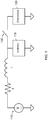
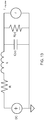
- FIG. 1 shows an example of a power distribution network (PDN) for distributing power from a DC power supply 110 to an upstream circuit 115 and a downstream circuit 120.
- the inductor L and the resistor R in FIG. 1 model inductance and resistance, respectively, of board and packaging interconnects between the power supply 110 and the circuits 115 and 120.
- the upstream circuit 115 and the downstream circuit 120 may be located on the same die.
- the PDN may employ power gating to conserve power.
- the PDN includes a power switch 130 for selectively connecting the downstream circuit 120 to the power supply 110.
- a power management circuit (not shown) turns on the power switch 130 to supply power to the downstream circuit 120.
- the power management circuit turns off the power switch 130 to disconnect the power supply 110 from the downstream circuit 120. This reduces power consumption when the downstream circuit 120 is inactive.
- the power switch 130 It is desirable for the power switch 130 to have a very low resistance when the downstream circuit 120 is active to minimize the IR (current (I) times resistance (R)) voltage drop across the power switch 130.
- I current
- R resistance
- the large voltage droop is caused by capacitors in the downstream circuit 120, which have approximately no charge when the downstream circuit 120 is first awakened from the inactive state (when power switch 130 is first closed).
- the size of the voltage droop is a function of the capacitance of the downstream circuit 120.
- equation (1) provides a good approximation of the voltage droop.
- the voltage droop can be large when the capacitance of the downstream circuit 120 is large relative to the capacitance of the upstream circuit 115. For example, when C up and C down are approximately equal, the voltage droop is approximately 50%, which is unacceptable high in most cases.
- a large voltage droop is undesirable because it can cause logic in the upstream circuit 115 to malfunction.
- a large voltage droop can also cause propagation delays in the upstream circuit 115 to increase, which can lead to timing problems in the upstream circuit 115. Therefore, it is important to keep the voltage droop within an acceptable limit (e.g., 5%) to ensure that the upstream circuit 115 functions properly.
- One approach to keep the voltage droop within an acceptable limit is to implement the power switch 130 using a variable-resistance power switch.
- the power switch 130 When the downstream circuit 120 is first awakened, the power switch 130 has a relatively high resistance to limit the rate of charge transfer from the upstream circuit 115 to the downstream circuit 120, and therefore reduce the voltage droop.
- the resistance of the power switch 130 decreases over time, providing time for charge from the power supply 110 to power up the downstream circuit 120 through the inductor L.
- the resistance of the switch becomes low.
- the variable-resistance power switch 130 may be implemented using a plurality of switches (e.g., transistor switches) coupled in parallel. When the downstream circuit 120 is awakened, the switches may be turned on over a period of time, in which the resistance of the power switch 130 decreases as more of the switches are turned on.
- the switches may include one or more weak switches (high-resistance switches) and one or more strong switches (low-resistance switches).
- a weak switch may have a resistance that is 10-20 times higher than the resistance of a strong switch.
- the weak switches may be turned on first to prevent a large voltage droop while the strong switches may be turned when the voltage at the power rail of the downstream circuit 120 settles to a voltage close to the nominal supply voltage.
- the resistance of the power switch 130 may be adjusted to prevent a large voltage droop at the upstream circuit 115 when the downstream circuit 120 is first awakened.
- the size of the voltage droop at the upstream circuit 115 and the wakeup time of the downstream circuit 120 There is a tradeoff between the size of the voltage droop at the upstream circuit 115 and the wakeup time of the downstream circuit 120.
- Increasing the initial resistance of the power switch 130 reduces the voltage droop at the expense of increasing the wakeup time. Therefore, it is important to accurately model the capacitance of the downstream circuit 120 in order to design a power switch 130 that optimizes both voltage droop and wakeup time.
- FIG. 2 shows an example of the downstream circuit 120 comprising an inverter formed by a P-type field effect transistor (PFET) 210 and an N-type field effect transistor (NFET) 220.
- the circuit 120 also comprises a first capacitor C1, a second capacitor C2, and a third capacitor C3.
- the first capacitor C1 represents an intrinsic capacitance of the PEFT 210 (e.g., N-well capacitance of the PFET 210)
- the second capacitance C2 represents parasitic capacitance of a wire connected to the output of the inverter
- the third capacitance C3 represents an intrinsic capacitance of the NEFT 220 (e.g., drain-to-body capacitance of the NFET 220).
- Resistor R1 in FIG. 2 represents resistance of the wire.
- the downstream circuit 120 may include many inverters and/or other logic devices.
- the capacitors in the downstream circuit 120 are discharged due to leakage current, and the voltage at the supply rail 222 of the downstream circuit 120 is approximately zero volts.
- the PFET 210 is initially turned off. This is because the source-to-gate voltage of the PFET 210 is initially well below the absolute threshold voltage V th of the PFET 210.
- the second capacitor C2 and the third capacitor C3 are initially isolated from the PDN, and therefore do not contribute to the capacitance of the downstream circuit 120 initially seen by the PDN.
- the PFET 210 turns on. This creates a channel between the source and drain of the PFET 210, thereby opening a path between the PDN and the second and the third capacitors C2 and C3.
- the PDN sees more of the capacitance from the second and third capacitors C2 and C3.
- the capacitance of the downstream circuit 120 seen by the PDN increases.
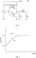
- FIG. 3 shows the capacitance 310 of the downstream circuit 120, as seen by the PDN, as a function of voltage at the supply rail 222.
- the power switch 130 When the power switch 130 is first turned on, the voltage at the supply rail 222 is approximately zero volts, and the capacitance 310 is C initial , which includes the capacitance of the first capacitor C1.
- the PFET 210 turns on, opening a path between the PDN and the second and third capacitors C2 and C3.
- the capacitance 310 seen by the PDN increases with increasing voltage.
- the PFET 210 When the voltage reaches the absolute threshold voltage V th of the PFET 210, the PFET 210 is fully turned on, and the capacitance 310 seen by the PDN approaches C final , which is the capacitance of the downstream circuit 120 when the downstream circuit 120 is fully powered up.
- the capacitance of the second capacitor C2 is not necessarily voltage dependent itself.
- the capacitance of the second capacitor C2, as seen by the PDN, is voltage dependent in this example because the path between the PDN and the second capacitor C2 through the PFET 210 (and hence the ability of the PDN is see the capacitance of the second capacitor C2) is voltage dependent.
- capacitors may also contribute to the voltage-dependent capacitance of the downstream circuit 120 besides the capacitors shown in the example in FIG. 3 .
- the example in FIG. 3 illustrates just one of many ways in which the capacitance of the downstream circuit 120 may be voltage dependent.
- the capacitance of the downstream circuit 120 increases with increasing voltage. This is because transistors within the downstream circuit 120 turn on with increasing voltage, causing the transistors to open paths between the PDN and capacitors within the downstream circuit 120.
- conventional modeling techniques simply model the capacitance of the downstream circuit 120 as a fixed capacitance approximately equal to C final . This is represented by the dashed line 320 in FIG. 3 . Therefore, in this example, conventional modeling techniques greatly overestimate the capacitance initially seen by the PDN, which leads to a large overestimation of voltage droop.
- Embodiments of the present disclosure provide techniques for modeling the voltage-dependent capacitance of a downstream circuit, thereby allowing a circuit designer to better optimize the resistance of a power switch compared with modeling techniques that model the capacitance of a downstream circuit 120 as a fixed capacitance. Embodiments of the present disclosure also provide techniques for modeling the voltage-dependent resistance of a downstream circuit.
- the voltage-dependent capacitance and resistance of a downstream circuit 120 are estimated by fitting a voltage-dependent RC circuit model of the downstream circuit 120 to measured impedances of the downstream circuit 120 obtained using, for example, a computer simulator (e.g., a simulation program with integrated circuit emphasis (SPICE) simulator).
- a computer simulator e.g., a simulation program with integrated circuit emphasis (SPICE) simulator.
- SPICE simulation program with integrated circuit emphasis
- the term "measurement” may refer to a measurement performed on a computer simulation of a device or a measurement of a physical device.
- the impedance of the downstream circuit 120 is measured at each one of a plurality of different DC voltages, which may span a voltage range anywhere between zero volts and the supply voltage of the PDN.
- the RC model of the downstream circuit 120 is fitted to the measured impedance at the DC voltage to determine the capacitance and resistance of the downstream circuit 120 at the DC voltage.
- the capacitance and resistance of the downstream circuit 120 are determined at each one of the plurality of different DC voltages, thereby characterizing the voltage-dependences of the capacitance and resistance of the downstream circuit 120 over the voltage range of the DC voltages.
- FIG. 4 below shows an exemplary test setup for measuring the impedance of a downstream circuit 120 using, for example, a computer simulator, in which the downstream circuit 120 is treated as a nonlinear device under test (DUT) 410.
- the DUT 410 is DC biased by a DC voltage source 420 and excited by a small AC voltage source 430 (e.g., microvolt amplitude) over a frequency range (e.g., zero to 100 MHz).
- the DC voltage source 420 may be sequentially set to each one of a plurality of different DC voltages, in which the impedance of the DUT 410 is measured over the frequency range at each DC voltage, as discussed further below.
- the computer simulator measures the S-parameter of the DUT 410 over the frequency range at each DC voltage.
- the computer simulator provides a measurement of the impedance Z of the DUT 410 over the frequency range at each DC voltage.
- FIG. 5 shows an example of a parallel RC circuit model 510 that may be used.
- the RC model 510 comprises a voltage-dependent capacitor C(V) in parallel with a voltage-dependent resistor R(V), and has a single pole.
- the parallel RC model 510 works well when the DUT 410 has a dominate pole within the frequency range of interest, and therefore can be accurately modeled as a parallel RC circuit.
- a method for determining the capacitance and resistance of the DUT 410 at a particular DC voltage using the measured impedance Z of the DUT 410 at the DC voltage and the RC model will now be described according to one embodiment.
- the resistance of the DUT 410 at the DC voltage is equal to the measured impedance Z of the DUT 410 at the DC voltage and a frequency of zero. This is because the impedance of the RC model is equal to the resistance when the frequency is zero. In this case, the resistance of the DUT 410 may be represented by Z
- s 0 .
- s 0 1 + sCZ
- s 0 where Z meas (s) represents the measured impedance at the DC voltage as a function of frequency, Z
- s 0 1 + sCZ
- s 0
- s 0 represents the resistance of the RC model at the DC voltage (as discussed above).
- the above equation determines the optimal capacitance C opt that minimizes the error between the measured impedance at the DC voltage and the impedance of the RC model over the frequency range.
- the error may be minimized using a gradient descent algorithm or other type of algorithm.
- the optimal capacitance C opt provides an estimate of the capacitance of the DUT 410 at the DC voltage.
- the method described above may be repeated for each one of the plurality of DC voltages to determine the resistance and capacitance of the DUT 410 at each DC voltage, and therefore characterize the voltage-dependencies of the resistance and capacitance of the DUT 410 over the voltage range of the DC voltages.
- the resistance and capacitance of the DUT 410 at a particular DC voltage may also be determined using a direct pole-fitting method.
- the pole-fitting method described above may be repeated for each one of the plurality of DC voltages to determine the resistance and capacitance of the DUT 410 at each DC voltage, and therefore characterize the voltage-dependencies of the resistance and capacitance of the DUT 410 over the voltage range of the DC voltages.
- modeling techniques described above may be used to model the voltage-dependent capacitances of different types of logic devices including inverters, NAND gates, NOR gates and other logic devices.
- FIG. 6A shows an example in which any one of the modeling techniques described above may be used to determine the voltage-dependent capacitance of an inverter 605 with the input of the inverter 605 driven low.
- the gates of the PFET 610 and the NFET 620 are coupled to ground via a resistance 630.
- the resistor 630 may have a resistance equal to or greater than the resistance of a driver that will drive the input of the inverter 605 low in a downstream circuit.
- the voltage-dependent capacitance of the inverter 605 may then be determined by performing one of the modeling techniques described above with the inverter 605 acting as the DUT 410.
- FIG. 6B shows another example in which any one of the modeling techniques described above may be used to determine the voltage-dependent capacitance of the inverter 605 with the input of the inverter 605 driven high.
- the gates of the PFET 610 and the NFET 620 are coupled to supply rail 622 via a resistance 640.
- the resistor 640 may have a resistance equal to or greater than the resistance of a driver that will drive the input of the inverter 605 high in a downstream circuit.
- the voltage-dependent capacitance of the inverter 605 may then be determined by performing one of the modeling techniques described above with the inverter 605 acting as the DUT 410.
- the voltage-dependent capacitance of the inverter 605 may be characterized for two different input logic states: one in which the input of the inverter 605 is driven low (logic 0) and another in which the input of the inverter 605 is driven high (logic 1).
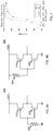
- FIG. 7 is a plot showing an example of the voltage-dependent capacitances of the inverter 605 for the two input logic states. As shown in FIG.
- the capacitance of the inverter 605 for input logic state 0 dramatically increases once the absolute threshold voltage (e.g., 500 mV) of the PFET 610 is reached and the capacitance of the inverter 605 for input logic state 1 dramatically increases once the threshold voltage (e.g., 450 mV) of the NFET 620 is reached.
- the capacitances for both states stays approximately constant when the voltage approaches the nominal supply voltage.
- the inputs to the downstream circuit 120 are typically set to predetermined values.
- the state of each node in the downstream circuit 120 at power up is known, and therefore the input logic state of the inverter 605 is known. This allows a circuit designer to select the appropriate voltage-dependent capacitance model for the inverter 605 in determining the initial resistance of the power switch 130, as discussed further below.
- the voltage-dependent capacitances of the inverter 605 for the two different states are determined without a parasitic-wire capacitive load coupled to the output of the inverter 605.
- any one of the modeling techniques described above may also be performed on the inverter 605 with a parasitic-wire capacitive load coupled to the output of the inverter 605 to account for the effects of parasitic-wire capacitance.
- FIG. 8 shows an example of a two-input NAND gate 810 comprising two PFETs 812 and 815 and two NFETs 820 and 825.
- the NAND gate 810 has four different input logic states: one in which both inputs 830 and 832 are driven low (logic 00), one in which both inputs 830 and 832 are driven high (logic 11), and two in which the inputs 830 and 832 are oppositely driven (logic 01 and 10).
- An input may be driven low by coupling the input to ground via a resistor, and an input may be driven high by coupling the input to the supply rail 822 via a resistor.
- FIG. 9 is a plot showing an example of the voltage-dependent capacitances of the NAND gate 810 for the four different input logic states.
- FIG. 10 shows an example of a two-input NOR gate 1010 comprising two PFETs 1012 and 1015 and two NFETs 1020 and 1025.
- the NOR gate 1010 has four different input logic states: one in which both inputs 1030 and 1032 are driven low (logic 00), one in which both inputs 1030 and 1032 are driven high (logic 11), and two in which the inputs 1030 and 1032 are oppositely driven (logic 01 and 10).
- An input may be driven low by coupling the input to ground via a resistor, and an input may be driven high by coupling the input to the supply rail 1022 via a resistor.
- FIG. 11 is a plot showing an example of the voltage-dependent capacitances of the NOR gate 1010 for the four different input logic states.
- the modeling techniques described above may be used to determine the voltage-dependent capacitances of various logic devices in a downstream circuit 120 including inverters, NAND gates, and NOR gates.
- Inverters, NAND gates and NOR gates form a universal logic set that can be used to implement various logic functions in a downstream circuit.
- the voltage-dependent capacitances of a plurality of logic devices may be determined separately and summed together to determine the voltage-dependent capacitance of a downstream circuit 120 comprising the plurality of logic devices.
- embodiments of the present disclosure model each logic device using a parallel RC circuit model. As a result, the voltage-dependent capacitances of the logic devices are in parallel, and can therefore be summed.
- the input logic state of the device when the downstream circuit 120 is first powered up is determined, and the voltage-dependent capacitance of the device for the determined input logic state is used in determining the voltage-dependent capacitance of the downstream circuit.
- this embodiment provides a computational efficient method for determining the voltage-dependent capacitance of a system comprising many logic devices.
- the voltage-dependent capacitance of a circuit comprising a plurality of logic devices may be determined by performing any one of the modeling techniques described above on the entire downstream circuit.
- the input logic state of each logic device is set the input logic state of the device when the circuit is first powered up.
- FIG. 12 shows a method 1200 for determining voltage-dependent capacitance of a circuit according to an embodiment of the present disclosure.
- a parameter of the circuit is measured at each one of a plurality of different voltages. For example, the impedance of the circuit over a frequency range may be measured at each voltage.
- a capacitance of the circuit at the voltage is determined by fitting an RC model of the circuit to the measured parameter of the circuit at the voltage. For example, for each voltage, the RC model of the circuit may be fitted to the measured impedance of the circuit at the voltage.
- the voltage-dependent capacitance of the downstream circuit 120 is estimated by measuring the impulse response of the PDN coupled to the downstream circuit.
- FIG. 13 shows an exemplary test setup, in which the downstream circuit 120 is biased by a DC power supply through a resistance R and inductor L of the PDN.
- the downstream circuit 120 is depicted as a voltage-dependent RC circuit.
- the DC power supply applies a plurality of different DC voltages to the downstream circuit. At each DC voltage, a test device excites the PDN with an impulse signal Impulse, and measures the resulting impulse response.
- the resonant frequency may be determined by taking a Fourier Transform of the measured impulse response.
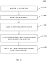
- FIG. 14 shows a method 1400 for determining the capacitance of the downstream circuit 120 at a particular DC voltage, in which the downstream circuit 120 is coupled to a PDN.
- the PDN is biased at the DC voltage.
- PDN resonance is excited. This may be done by exciting the PDN with an impulse signal.
- the impulse response of the PDN is measured.
- the resonant frequency is calculated based on the measured impulse response.
- the capacitance of the downstream circuit 120 at the DC voltage is calculated based on the resonant frequency. For example, the capacitance may be calculated using equation (9).
- the method 1400 may be repeated for each one of a plurality of different DC voltages to determine the capacitance of the downstream circuit 120 at each one of the plurality of DC voltages, and therefore characterize the voltage-dependent capacitance of the downstream circuit 120.
- modeling techniques according to embodiments of the present disclosure model the voltage-dependent capacitance of the downstream circuit. This allows a circuit designer to more accurately determine the capacitance of the downstream circuit 120 when the downstream circuit 120 is first awakened, and therefore better optimize the power switch 130 to reduce wakeup time while still keeping the voltage droop at the upstream circuit 115 within a particular voltage-droop limit (e.g., 5%). For example, modeling techniques according to embodiments of the present disclosure determine that the capacitance of a downstream circuit 120, as seen by the PDN, is lower when the power switch 130 is first turned on compared with conventional modeling techniques. Using this knowledge, the initial resistance of the power switch 130 can be made lower to reduce wakeup time while still keeping the voltage droop within a voltage-droop limit (e.g., 5%).
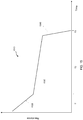
- FIG. 15 shows an example of a resistance profile 1510 of the power switch 130 that can be determined using modeling techniques according to embodiments of the present disclosure.
- the resistance profile 1510 represents the resistance of the power switch 130 as a function of time.
- the resistance profile 1510 may be divided into a first time interval T1, a second time interval T2, and a third time interval T3.
- the first time interval T1 begins at the time when the power switch 130 is first turned on to power up the downstream circuit 120.
- the resistance of the power switch 130 decreases at a relatively fast rate 1520.
- the resistance of the power switch 130 may decrease at a much faster rate than a rate that would have be determined using conventional modeling techniques. This is because embodiments of the present disclosure accurately determine that the capacitance of the downstream circuit 120, as seen by the PDN, is lower when the power switch is first turned on, and therefore that the resistance of the power switch 130 can decrease at a faster rate while still staying within the voltage-droop limit.
- the capacitance of the downstream circuit 120 is lower when the power switch 130 is first turned on compared to when the power switch has been turned on long enough for the power rail of the downstream circuit 120 to reach a voltage at which transistors in the downstream circuit 120 are turned on.
- the first time interval T1 may end at a time when the power rail of the downstream circuit 120 reaches a voltage approximately equal to a threshold voltage of transistors within the downstream circuit.
- the capacitance of the downstream circuit increases as transistors within the downstream circuit 120 turn on and open paths to capacitors within the downstream circuit.
- the threshold voltage of the transistors may refer to an average of the absolute threshold voltages of the transistors.
- the resistance of the power switch 130 decreases at a slower rate 1530 compared with the first time interval T1.
- the resistance of the power switch 130 may decrease at a rate that is 50% or more slower. This is because the capacitance of the downstream circuit, as seen by the PDN, is higher during the second time interval T2 compared with the first time interval T1.
- the voltage at the power rail of the downstream circuit 120 may be above the threshold voltage of transistors within the downstream circuit, in which case the transistors are turned on.
- the capacitance of the downstream circuit, as seen by the PDN may be close to its final value during most or all of the second time interval T2.
- the second time interval T2 may end at a time when the voltage at the power rail of the downstream circuit 120 settles to a voltage that is close to the nominal supply voltage.
- the second time interval T2 may end when the voltage difference between the downstream circuit 120 and the nominal supply voltage is approximately equal to or smaller than the voltage-droop limit.
- the resistance of the power switch 130 may decrease at a faster rate 1540 compared with the second time interval T2 and the first time interval T1. This is because voltage droop is confined to the voltage difference between the downstream circuit 120 and the nominal supply voltage. Thus, when the voltage difference is small, even a large drop in the resistance of the power switch 130 only results in a small voltage droop.
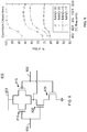
- FIG. 16 shows an example of a power switch 1605 for implementing the resistance profile 1510 shown in FIG. 15 according to an embodiment of the present disclosure.
- the power switch 1605 comprises a first switch circuit 1610, a second switch circuit 1630, and a third switch 1650.
- the first switch circuit 1610 implements the portion of the resistance profile 1510 corresponding to the first time interval T1, and comprises a first set of switches 1615-1 to 1615-6 and a first set of delay elements 1612-1 to 1612-5. Although six switches are shown in FIG. 16 for ease of illustration, it is to be appreciated that the first set of switches 1615-1 to 1615-6 may comprise many more switches (e.g., hundreds or thousands of switches). Each of the switches 1615-1 to 1615-6 is coupled between the upstream circuit 115 and the downstream circuit 120. It is to be appreciated that FIG. 16 is not drawn to scale, and that the sizes of the switches are exaggerated with respect to the upstream circuit 115 and downstream circuit 120 for ease of illustration. In the example shown in FIG.
- each of the switches 1615-1 to 1615-6 is implemented with a PFET.
- the delay elements 1612-1 to 1612-5 are coupled in series, in which the output of each delay element 1612-1 to 1612-5 is coupled to the gate of one of the switches 1615-1 to 1615-6.
- a power management circuit 1606 inputs a signal 1608 to the first set of delay elements 1612-1 to 1612-5 to begin turning on the first set of switches 1615-1 to 1615-6.
- the delay elements 1612-1 to 1612-5 sequentially turn on the switches 1615-1 to 1615-6.
- the delay between adjacent switches turning on is approximately equal to the delay of the delay element between the adjacent switches.
- the delay between switches 1615-1 and 1615-2 turning on is approximately equal to the delay of delay element 1612-1.
- the second switch circuit 1630 implements the portion of the resistance profile 1510 corresponding to the second time interval T2, and comprises a second set of switches 1635-1 to 1635-6 and the second set of delay elements 1632-1 to 1632-5.
- the second set of switches 1635-1 to 1635-6 may comprise many more switches (e.g., hundreds or thousands of switches). It is also to be appreciated that the first and second set of switches may have different numbers of switches.
- Each of the switches 1635-1 to 1635-6 is coupled between the upstream circuit 115 and the downstream circuit 120. In the example shown in FIG. 16 , each of the switches 1635-1 to 1635-6 is implemented with a PFET.
- the delay elements 1632-1 to 1632-5 are coupled in series, in which the output of each delay element 1632-1 to 1632-5 is coupled to the gate of one of the switches 1635-1 to 1635-6.
- a signal 1628 is input to the second set of delay elements 1632-1 to 1632-5 to begin turning on the second set of switches 1635-1 to 1635-6.
- the signal 1628 may be a delayed version of the signal output by the first set of switches 1612-1 to 1612-5.
- the signal output by the first set of delay elements 1612-1 to 1612-5 may be input to the second set of delay elements 1632-1 to 1632-5 after being delayed by delay element 1620.
- the signal output by the first set of delay elements 1612-1 to 1612-5 may be input back to the power management circuit 1606 as an acknowledgement that the first set of switches 1615-1 to 1615-6 have been turned on, and the power management circuit 1606 may launch the signal 1628 after a timed delay to start turning on the second set of switches 1635-1 to 1635-6. As the signal 1628 propagates through the second set of delay elements 1632-1 to 1632-5, the delay elements 1632-1 to 1632-5 sequentially turn on the switches 1635-1 to 1635-6.
- the third switch 1650 implements the portion of the resistance profile 1510 corresponding to the third time interval T3.
- the third switch 1650 is coupled between the upstream circuit 115 and the downstream circuit 120.
- the third switch 1650 may be implemented using one or more strong switches (low-resistance switches), in which each strong switch may have a much lower resistance (i.e., much higher conductance) than each of the switches in the first and second set of switches.
- a signal 1658 is input to the third switch 1650 to turn on the third switch 1650.
- the signal 1658 may be a delayed version of the signal output by the second set of delay elements 1632-1 to 1632-5.
- the signal output by the second set of delay elements 1632-1 to 1632-5 may be input to the third switch 1650 after being delayed by delay element 1640.
- the signal output by the second set of delay elements 1632-1 to 1632-5 may be input back to the power management circuit 1606 as an acknowledgement that the second set of switches 1635-1 to 1635-6 have been turned on, and the power management circuit 1606 may launch the signal 1658 after a timed delay to turn on the third switch 1650.
- the third switch 1650 comprises a plurality of strong switches
- the strong switches may be turned at approximately the same time or the strong switches may be turned on sequentially using a set of delay elements.
- the power switch 1605 has a variable resistance, in which the resistance of the power switch 1605 at a given time depends on the switches 1615-1 to 1615-6, 1635-1 to 1635-6, and 1650 that are turned on at the given time. The resistance is lowest when all of the switches are turned on.
- the delay elements 1612-1 to 1612-5, 1620, 1632-1 to 1632-5, and 1640 control the timing sequence for turning on the switches 1615-1 to 1615-6, 1635-1 to 1635-6, and 1650 during power up, and therefore control the resistance of the power switch 1605 during power up.
- the delay elements 1612-1 to 1612-5, 1620, 1632-1 to 1632-5, and 1640 may form a switch control circuit configured to control the resistance of the power switch 1605 during power up.
- the resistance of the power switch 130 decreases at a faster rate during the first time interval T1 compared with the second time interval T2. This may be implemented using the power switch 1605 in FIG. 16 according to various embodiments of the present disclosure.
- the resistance of each switch in the first set of switches 1615-1 and 1615-6 may be lower than the resistance of each switch in the second set of switches 1635-1 to 1635-6. As a result, when one of the switches in the first set of switches 1615-1 to 1615-6 turns on, the resistance of the power switch 1605 drops by a larger amount than when one of the switches in the second set of switches 1635-1 to 1635-6 turns on.
- the delay of each delay element in the first set of delay elements 1612-1 to 1612-5 may be shorter than the delay of each delay element in the second set of delay elements 1632-1 to 1632-5. This causes the switches in the first set of switches 1615-1 to 1615-6 to turn on at a faster rate compared with the switches in the second set of switches 1635-1 to 1635-6, and therefore decrease the resistance of the power switch 1605 at a faster rate.
- each of the switches in the first set of switches 1615-1 to 1615-6 may have approximately the same resistance as each of the switches in the second set of switches 1635-1 to 1635-6.
- two or more switches in the first set of switches 1615-1 to 1615-6 may be turned on at a time in parallel, an example of which is shown in FIG. 17 .
- the first switch circuit 1710 comprises a set of delay elements 1712-1 to 1712-2, in which the output of each delay element turns on two of the switches in parallel.
- the resistance of the power switch 1705 decreases at a faster rate during the first time interval T1.
- each of the switches in the first set of switches 1615-1 to 1615-6 may have approximately the same resistance as each of the switches in the second set of switches 1635-1 to 1635-6.
- two or more switches in the second set of switches 1635-1 to 1635-6 may also be turned on at a time in parallel.
- a larger number of switches in the first set of switches 1615-1 to 1615-6 may be turned on at a time compared with the second set of switches 1635-1 to 1635-6.
- twice as many switches in the first set of switches 1615-1 to 1615-6 may be turned on at a time compared with the second set of switches 1635-1 to 1635-6.
- any two or more of the embodiments discussed above may be used in combination to make the resistance of the power switch decrease at a faster rate during the first time interval T1 compared with the second time interval T2.
- the switches in the first set of switches 1615-1 to 1615-6 may both have a lower resistance than the switches in the second set of the switches 1635-1 to 1615-6 and turn on at a faster rate.
- the resistance profile 1510 is shown as being piece-wise linear in FIG. 15 for ease of illustration, it is to be appreciated that the resistance profile 1510 is not limited to this example.
- the resistance of the power switch 130 does not need to decrease at a uniform rate within one of the time intervals.
- the drop in resistance ⁇ R may be given by the difference between the resistance of the power switch after the first switch during the first time interval T1 turns on and the resistance of the power switch after the last switch during the first time interval T1 turns on. This may be done so that the off resistance of the power switch 130 is not included in the calculation.
- the drop in resistance ⁇ R may be given by the difference between the resistance of the power switch after the first switch during the second interval T2 turns on and the resistance of the power switch after the last switch during the second time interval T2 turns on.
- the drop in resistance ⁇ R may be given by the difference between the resistance of the power switch after the last switch during the first time interval T1 turns on and the resistance of the power switch after the last switch during the second time interval T2 turns on.
- the drop in resistance ⁇ R may be given by the difference between the resistance of the power switch after the first switch during the third time interval T3 turns on and the resistance of the power switch after the last switch during the third time interval T3 turns on.
- the drop in resistance ⁇ R may be given by the difference between the resistance of the power switch after the last switch during the second time interval T2 turns on and the resistance of the power switch after the last switch during the third time interval T3 turns on.
- the boundary between the first and second time intervals T1 and T2 may correspond to a time when the voltage of the downstream circuit 120 is approximately equal to the threshold voltage of transistors in the downstream circuit 120. In general, this boundary may correspond to a time when the voltage is some percentage of the threshold voltage (e.g., 70% or more of the threshold voltage, 80% or more of the threshold voltage, or 90% or more of the threshold voltage).
- the boundary between the second and third time intervals T2 and T3 may correspond to a time when the voltage of the downstream circuit 120 settles to a voltage that is close to the nominal supply voltage.
- this boundary may correspond to a time when the voltage is some percentage of the nominal supply voltage (e.g., 90% or more of the nominal supply voltage).
- FIGS. 18A and 18B show a method 1800 for power gating in a system according to an embodiment of the present disclosure.
- the system comprising a circuit (e.g., downstream circuit 120) and a power switch (e.g., power switch 130) coupled between the circuit and a power supply.
- a circuit e.g., downstream circuit 120
- a power switch e.g., power switch 130
- step 1810 the power switch is turned on when the circuit is to be awakened from an inactive state, as shown in FIG. 18A .
- Step 1810 further comprises steps 1810A and 1810B shown in FIG. 18B .
- a resistance of the power switch is decreased at a first rate during a first time interval.
- the resistance of the power switch is decreased at a second rate during a second time interval immediately following the first time interval, wherein the first rate is greater than the second rate, and a boundary between the first and second time intervals corresponds to a time at which a voltage of the circuit approximately reaches a threshold voltage of transistors in the circuit.
- the threshold voltage of the transistors may refer to an average of the absolute threshold voltages of the transistors.
- circuits described herein may be realized using a variety of transistor types, and are therefore not limited to the particular transistor types shown in the figures.
- transistor types such as bipolar junction transistors, junction field effect transistor or any other transistor type may be used.
- circuits described herein may be fabricated with various IC process technologies such as CMOS, bipolar junction transistor (BJT), bipolar-CMOS (BiCMOS), silicon germanium (SiGe), gallium arsenide (GaAs), etc.
- a method described herein may be embodied in a computer program (e.g., software) stored on a computer-readable medium, in which the computer program comprises code (instructions) that is executable by a processor (e.g., a general-purpose processor) for performing the method.
- the computer-readable medium may comprise a RAM memory, a flash memory, a hard disk, a removable disk, a CD-ROM or other optical disk storage, or any other form of computer-readable medium known in the art.
Landscapes
- Engineering & Computer Science (AREA)
- Physics & Mathematics (AREA)
- General Physics & Mathematics (AREA)
- Computer Hardware Design (AREA)
- Theoretical Computer Science (AREA)
- General Engineering & Computer Science (AREA)
- Geometry (AREA)
- Evolutionary Computation (AREA)
- Microelectronics & Electronic Packaging (AREA)
- Logic Circuits (AREA)
- Design And Manufacture Of Integrated Circuits (AREA)
- Direct Current Feeding And Distribution (AREA)
- Measurement Of Resistance Or Impedance (AREA)
- Measurement Of Current Or Voltage (AREA)
- Electronic Switches (AREA)
Applications Claiming Priority (2)
| Application Number | Priority Date | Filing Date | Title |
|---|---|---|---|
| US14/157,451 US9429610B2 (en) | 2014-01-16 | 2014-01-16 | Voltage dependent die RC modeling for system level power distribution networks |
| PCT/US2015/011658 WO2015109125A1 (en) | 2014-01-16 | 2015-01-15 | Voltage dependent die rc modeling for system level power distribution networks |
Publications (2)
| Publication Number | Publication Date |
|---|---|
| EP3095053A1 EP3095053A1 (en) | 2016-11-23 |
| EP3095053B1 true EP3095053B1 (en) | 2019-07-24 |
Family
ID=52440885
Family Applications (1)
| Application Number | Title | Priority Date | Filing Date |
|---|---|---|---|
| EP15702071.0A Active EP3095053B1 (en) | 2014-01-16 | 2015-01-15 | Voltage dependent die rc modeling for system level power distribution networks |
Country Status (7)
Families Citing this family (6)
| Publication number | Priority date | Publication date | Assignee | Title |
|---|---|---|---|---|
| JP6623696B2 (ja) * | 2015-11-09 | 2019-12-25 | 株式会社ソシオネクスト | 電源装置及び半導体装置 |
| KR102236526B1 (ko) * | 2017-11-28 | 2021-04-05 | 에스케이하이닉스 주식회사 | 시간-도메인 반사 측정 신호를 이용한 고주파대역 정전용량 추출 방법, 장치 및 이를 구현하는 컴퓨터로 읽을 수 있는 기록 매체 |
| KR102039556B1 (ko) | 2018-08-08 | 2019-11-01 | (주)휴윈 | 전력분배망 임피던스 분석 방법 및 이를 기록한 컴퓨터 판독 가능한 기록매체, 전력분배망 임피던스 분석 장치 |
| GB202018942D0 (en) * | 2020-12-01 | 2021-01-13 | Appleyard Lees Ip Llp | Temperature Estimation |
| CN113761793B (zh) * | 2021-08-16 | 2024-02-27 | 固德威技术股份有限公司 | 逆变器输出阻抗检测装置及方法、逆变器运行控制方法 |
| TWI828550B (zh) * | 2023-03-01 | 2024-01-01 | 智原科技股份有限公司 | 佈線方法、電腦程式產品及與其相關之積體電路 |
Family Cites Families (40)
| Publication number | Priority date | Publication date | Assignee | Title |
|---|---|---|---|---|
| JP2940074B2 (ja) | 1990-05-28 | 1999-08-25 | 日本電気株式会社 | セラミックグリーンシート間の接着性評価方法 |
| US5461338A (en) | 1992-04-17 | 1995-10-24 | Nec Corporation | Semiconductor integrated circuit incorporated with substrate bias control circuit |
| JP3561012B2 (ja) | 1994-11-07 | 2004-09-02 | 株式会社ルネサステクノロジ | 半導体集積回路装置 |
| JP3708168B2 (ja) | 1995-06-13 | 2005-10-19 | 富士通株式会社 | 遅延装置 |
| JP2931776B2 (ja) | 1995-08-21 | 1999-08-09 | 三菱電機株式会社 | 半導体集積回路 |
| US5646543A (en) | 1995-10-12 | 1997-07-08 | Lucent Technologies Inc. | Integrated circuit having reduced inductive noise |
| KR100466457B1 (ko) | 1995-11-08 | 2005-06-16 | 마츠시타 덴끼 산교 가부시키가이샤 | 신호전송회로,신호수신회로및신호송수신회로,신호전송방법,신호수신방법및신호송수신방법과반도체집적회로및그제어방법 |
| US5694949A (en) | 1996-08-06 | 1997-12-09 | Pacesetter, Inc. | Variable capacitance emulation circuit for electrophysiology diagnostic device |
| JP3732914B2 (ja) | 1997-02-28 | 2006-01-11 | 株式会社ルネサステクノロジ | 半導体装置 |
| US5949253A (en) | 1997-04-18 | 1999-09-07 | Adaptec, Inc. | Low voltage differential driver with multiple drive strengths |
| US6233693B1 (en) | 1998-05-06 | 2001-05-15 | International Business Machines Corporation | Smart DASD spin-up |
| US6064223A (en) | 1998-07-08 | 2000-05-16 | Intel Corporation | Low leakage circuit configuration for MOSFET circuits |
| US6329874B1 (en) | 1998-09-11 | 2001-12-11 | Intel Corporation | Method and apparatus for reducing standby leakage current using a leakage control transistor that receives boosted gate drive during an active mode |
| US6184729B1 (en) | 1998-10-08 | 2001-02-06 | National Semiconductor Corporation | Low ground bounce and low power supply bounce output driver |
| US6225852B1 (en) | 1999-10-01 | 2001-05-01 | Advanced Micro Devices, Inc. | Use of biased high threshold voltage transistor to eliminate standby current in low voltage integrated circuits |
| JP3912960B2 (ja) | 2000-06-20 | 2007-05-09 | 株式会社東芝 | 半導体集積回路、論理演算回路およびフリップフロップ |
| US6744301B1 (en) | 2000-11-07 | 2004-06-01 | Intel Corporation | System using body-biased sleep transistors to reduce leakage power while minimizing performance penalties and noise |
| US6959404B2 (en) | 2001-08-23 | 2005-10-25 | Texas Instruments Incorporated | Extended dynamic range watchdog timer |
| DE60218225T2 (de) | 2002-01-23 | 2007-10-31 | Koninklijke Philips Electronics N.V. | Integrierte schaltung und batteriebetriebenes elektronisches gerät |
| JP3951773B2 (ja) | 2002-03-28 | 2007-08-01 | 富士通株式会社 | リーク電流遮断回路を有する半導体集積回路 |
| JP4052923B2 (ja) | 2002-10-25 | 2008-02-27 | 株式会社ルネサステクノロジ | 半導体装置 |
| JP4549026B2 (ja) | 2003-01-14 | 2010-09-22 | 富士通セミコンダクター株式会社 | 半導体集積回路 |
| US6977519B2 (en) | 2003-05-14 | 2005-12-20 | International Business Machines Corporation | Digital logic with reduced leakage |
| US6876252B2 (en) | 2003-06-28 | 2005-04-05 | International Business Machines Corporation | Non-abrupt switching of sleep transistor of power gate structure |
| DE102004036956B3 (de) | 2004-07-30 | 2006-03-23 | Infineon Technologies Ag | Logik-Aktivierungsschaltung |
| US7276932B2 (en) | 2004-08-26 | 2007-10-02 | International Business Machines Corporation | Power-gating cell for virtual power rail control |
| US7659746B2 (en) | 2005-02-14 | 2010-02-09 | Qualcomm, Incorporated | Distributed supply current switch circuits for enabling individual power domains |
| JP2008034667A (ja) * | 2006-07-31 | 2008-02-14 | Renesas Technology Corp | 半導体集積回路装置 |
| JP2008065732A (ja) * | 2006-09-11 | 2008-03-21 | Nec Electronics Corp | 半導体集積回路の設計方法及び設計システム |
| TW200910373A (en) * | 2007-06-08 | 2009-03-01 | Mosaid Technologies Inc | Dynamic impedance control for input/output buffers |
| JP2009105221A (ja) * | 2007-10-23 | 2009-05-14 | Nec Electronics Corp | 半導体集積回路装置 |
| US8570025B2 (en) | 2007-11-20 | 2013-10-29 | Ferfics Limited | Power delivery circuit with load current estimation based on monitoring nodes not on the power delivery path |
| JP4535134B2 (ja) * | 2008-01-16 | 2010-09-01 | ソニー株式会社 | 半導体集積回路およびその電源制御方法 |
| JP5211889B2 (ja) * | 2008-06-25 | 2013-06-12 | 富士通株式会社 | 半導体集積回路 |
| CN102804577B (zh) | 2009-06-25 | 2016-04-13 | 瑞典爱立信有限公司 | 开关模式电源中的电容确定 |
| US8063622B2 (en) * | 2009-10-02 | 2011-11-22 | Power Integrations, Inc. | Method and apparatus for implementing slew rate control using bypass capacitor |
| JP5541143B2 (ja) * | 2010-12-21 | 2014-07-09 | 富士通株式会社 | 半導体装置 |
| US8537593B2 (en) | 2011-04-28 | 2013-09-17 | Sandisk Technologies Inc. | Variable resistance switch suitable for supplying high voltage to drive load |
| US8427886B2 (en) | 2011-07-11 | 2013-04-23 | Lsi Corporation | Memory device with trimmable power gating capabilities |
| CN102592021B (zh) * | 2012-01-06 | 2013-08-14 | 北京航空航天大学 | 一种航空参数处理设备电源模块的fmis方法 |
-
2014
- 2014-01-16 US US14/157,451 patent/US9429610B2/en active Active
-
2015
- 2015-01-15 BR BR112016016463A patent/BR112016016463A2/pt not_active IP Right Cessation
- 2015-01-15 CN CN201580004761.7A patent/CN105917338B/zh active Active
- 2015-01-15 KR KR1020167021730A patent/KR102120754B1/ko active Active
- 2015-01-15 WO PCT/US2015/011658 patent/WO2015109125A1/en active Application Filing
- 2015-01-15 JP JP2016546845A patent/JP6553057B2/ja not_active Expired - Fee Related
- 2015-01-15 EP EP15702071.0A patent/EP3095053B1/en active Active
Non-Patent Citations (1)
| Title |
|---|
| None * |
Also Published As
| Publication number | Publication date |
|---|---|
| EP3095053A1 (en) | 2016-11-23 |
| BR112016016463A2 (pt) | 2017-08-08 |
| CN105917338A (zh) | 2016-08-31 |
| JP2017506328A (ja) | 2017-03-02 |
| WO2015109125A1 (en) | 2015-07-23 |
| US9429610B2 (en) | 2016-08-30 |
| CN105917338B (zh) | 2018-11-20 |
| JP6553057B2 (ja) | 2019-07-31 |
| KR20160108432A (ko) | 2016-09-19 |
| US20150198646A1 (en) | 2015-07-16 |
| KR102120754B1 (ko) | 2020-06-09 |
Similar Documents
| Publication | Publication Date | Title |
|---|---|---|
| EP3095053B1 (en) | Voltage dependent die rc modeling for system level power distribution networks | |
| US10559559B2 (en) | Integrated protection devices with monitoring of electrical characteristics | |
| Kaushik et al. | Crosstalk analysis for a CMOS-gate-driven coupled interconnects | |
| Agarwal et al. | Recent enhancements in BSIM6 bulk MOSFET model | |
| CN113691108A (zh) | 一种低边nmos的驱动电路 | |
| CN115843416A (zh) | 多偏置模式电流输送器、配置多偏置模式电流输送器、包括多偏置模式电流输送器的触摸传感系统以及相关的系统、方法和设备 | |
| US7436196B2 (en) | Method and apparatus for measuring die-level integrated circuit power variations | |
| KR102219822B1 (ko) | 전압 드룹의 제약에 의한 파워-게이트 섹션들의 크기조정 | |
| US20150108956A1 (en) | Switched mode power supply peak-efficiency detection | |
| Ida et al. | A physically-based behavioral snapback model | |
| US9638743B2 (en) | State-dependent capacitance estimation | |
| Kovačević et al. | FPGA low-power implementation of QRS detectors | |
| Ioannou et al. | A robust reliability methodology for accurately predicting Bias Temperature Instability induced circuit performance degradation in HKMG CMOS | |
| Lai et al. | LDMOS modeling | |
| CN104065041A (zh) | 电源保护电路 | |
| US20050050494A1 (en) | Power estimation based on power characterizations of non-conventional circuits | |
| US8464195B1 (en) | Integrated circuit clock analysis with macro models | |
| US11275879B2 (en) | Method for detecting hazardous high impedance nets | |
| Mahmoud et al. | Current source based standard-cell model for accurate timing analysis of combinational logic cells | |
| Zhang et al. | Power distribution network design optimization with on-die voltage-dependent leakage path | |
| Avolio et al. | Waveforms-based large-signal identification of transistor models | |
| KR20090120178A (ko) | 반도체 메모리 소자의 테스트 방법 | |
| Sahoo et al. | Explicit Delay and Power Estimation Method for CMOS Inverter Driving on-Chip RLC Interconnect Load | |
| Kar et al. | An explicit approach for delay evaluation for on-chip RC interconnects using beta distribution function by moment matching technique | |
| Palampougioukis et al. | An efficient model of the CMOS inverter for nanometer technologies |
Legal Events
| Date | Code | Title | Description |
|---|---|---|---|
| PUAI | Public reference made under article 153(3) epc to a published international application that has entered the european phase |
Free format text: ORIGINAL CODE: 0009012 |
|
| 17P | Request for examination filed |
Effective date: 20160608 |
|
| AK | Designated contracting states |
Kind code of ref document: A1 Designated state(s): AL AT BE BG CH CY CZ DE DK EE ES FI FR GB GR HR HU IE IS IT LI LT LU LV MC MK MT NL NO PL PT RO RS SE SI SK SM TR |
|
| AX | Request for extension of the european patent |
Extension state: BA ME |
|
| DAX | Request for extension of the european patent (deleted) | ||
| GRAP | Despatch of communication of intention to grant a patent |
Free format text: ORIGINAL CODE: EPIDOSNIGR1 |
|
| STAA | Information on the status of an ep patent application or granted ep patent |
Free format text: STATUS: GRANT OF PATENT IS INTENDED |
|
| RIC1 | Information provided on ipc code assigned before grant |
Ipc: G06F 17/50 20060101AFI20190201BHEP Ipc: G01R 31/28 20060101ALI20190201BHEP Ipc: G01R 27/26 20060101ALI20190201BHEP Ipc: G11C 5/14 20060101ALI20190201BHEP |
|
| INTG | Intention to grant announced |
Effective date: 20190228 |
|
| GRAS | Grant fee paid |
Free format text: ORIGINAL CODE: EPIDOSNIGR3 |
|
| GRAA | (expected) grant |
Free format text: ORIGINAL CODE: 0009210 |
|
| STAA | Information on the status of an ep patent application or granted ep patent |
Free format text: STATUS: THE PATENT HAS BEEN GRANTED |
|
| AK | Designated contracting states |
Kind code of ref document: B1 Designated state(s): AL AT BE BG CH CY CZ DE DK EE ES FI FR GB GR HR HU IE IS IT LI LT LU LV MC MK MT NL NO PL PT RO RS SE SI SK SM TR |
|
| REG | Reference to a national code |
Ref country code: GB Ref legal event code: FG4D |
|
| REG | Reference to a national code |
Ref country code: CH Ref legal event code: EP |
|
| REG | Reference to a national code |
Ref country code: DE Ref legal event code: R096 Ref document number: 602015034228 Country of ref document: DE |
|
| REG | Reference to a national code |
Ref country code: AT Ref legal event code: REF Ref document number: 1159052 Country of ref document: AT Kind code of ref document: T Effective date: 20190815 |
|
| REG | Reference to a national code |
Ref country code: IE Ref legal event code: FG4D |
|
| REG | Reference to a national code |
Ref country code: DE Ref legal event code: R079 Ref document number: 602015034228 Country of ref document: DE Free format text: PREVIOUS MAIN CLASS: G06F0017500000 Ipc: G06F0030000000 |
|
| REG | Reference to a national code |
Ref country code: NL Ref legal event code: MP Effective date: 20190724 |
|
| REG | Reference to a national code |
Ref country code: LT Ref legal event code: MG4D |
|
| REG | Reference to a national code |
Ref country code: AT Ref legal event code: MK05 Ref document number: 1159052 Country of ref document: AT Kind code of ref document: T Effective date: 20190724 |
|
| PG25 | Lapsed in a contracting state [announced via postgrant information from national office to epo] |
Ref country code: LT Free format text: LAPSE BECAUSE OF FAILURE TO SUBMIT A TRANSLATION OF THE DESCRIPTION OR TO PAY THE FEE WITHIN THE PRESCRIBED TIME-LIMIT Effective date: 20190724 Ref country code: PT Free format text: LAPSE BECAUSE OF FAILURE TO SUBMIT A TRANSLATION OF THE DESCRIPTION OR TO PAY THE FEE WITHIN THE PRESCRIBED TIME-LIMIT Effective date: 20191125 Ref country code: HR Free format text: LAPSE BECAUSE OF FAILURE TO SUBMIT A TRANSLATION OF THE DESCRIPTION OR TO PAY THE FEE WITHIN THE PRESCRIBED TIME-LIMIT Effective date: 20190724 Ref country code: AT Free format text: LAPSE BECAUSE OF FAILURE TO SUBMIT A TRANSLATION OF THE DESCRIPTION OR TO PAY THE FEE WITHIN THE PRESCRIBED TIME-LIMIT Effective date: 20190724 Ref country code: NL Free format text: LAPSE BECAUSE OF FAILURE TO SUBMIT A TRANSLATION OF THE DESCRIPTION OR TO PAY THE FEE WITHIN THE PRESCRIBED TIME-LIMIT Effective date: 20190724 Ref country code: SE Free format text: LAPSE BECAUSE OF FAILURE TO SUBMIT A TRANSLATION OF THE DESCRIPTION OR TO PAY THE FEE WITHIN THE PRESCRIBED TIME-LIMIT Effective date: 20190724 Ref country code: BG Free format text: LAPSE BECAUSE OF FAILURE TO SUBMIT A TRANSLATION OF THE DESCRIPTION OR TO PAY THE FEE WITHIN THE PRESCRIBED TIME-LIMIT Effective date: 20191024 Ref country code: FI Free format text: LAPSE BECAUSE OF FAILURE TO SUBMIT A TRANSLATION OF THE DESCRIPTION OR TO PAY THE FEE WITHIN THE PRESCRIBED TIME-LIMIT Effective date: 20190724 Ref country code: NO Free format text: LAPSE BECAUSE OF FAILURE TO SUBMIT A TRANSLATION OF THE DESCRIPTION OR TO PAY THE FEE WITHIN THE PRESCRIBED TIME-LIMIT Effective date: 20191024 |
|
| PG25 | Lapsed in a contracting state [announced via postgrant information from national office to epo] |
Ref country code: RS Free format text: LAPSE BECAUSE OF FAILURE TO SUBMIT A TRANSLATION OF THE DESCRIPTION OR TO PAY THE FEE WITHIN THE PRESCRIBED TIME-LIMIT Effective date: 20190724 Ref country code: IS Free format text: LAPSE BECAUSE OF FAILURE TO SUBMIT A TRANSLATION OF THE DESCRIPTION OR TO PAY THE FEE WITHIN THE PRESCRIBED TIME-LIMIT Effective date: 20191124 Ref country code: ES Free format text: LAPSE BECAUSE OF FAILURE TO SUBMIT A TRANSLATION OF THE DESCRIPTION OR TO PAY THE FEE WITHIN THE PRESCRIBED TIME-LIMIT Effective date: 20190724 Ref country code: GR Free format text: LAPSE BECAUSE OF FAILURE TO SUBMIT A TRANSLATION OF THE DESCRIPTION OR TO PAY THE FEE WITHIN THE PRESCRIBED TIME-LIMIT Effective date: 20191025 Ref country code: LV Free format text: LAPSE BECAUSE OF FAILURE TO SUBMIT A TRANSLATION OF THE DESCRIPTION OR TO PAY THE FEE WITHIN THE PRESCRIBED TIME-LIMIT Effective date: 20190724 Ref country code: AL Free format text: LAPSE BECAUSE OF FAILURE TO SUBMIT A TRANSLATION OF THE DESCRIPTION OR TO PAY THE FEE WITHIN THE PRESCRIBED TIME-LIMIT Effective date: 20190724 |
|
| PG25 | Lapsed in a contracting state [announced via postgrant information from national office to epo] |
Ref country code: TR Free format text: LAPSE BECAUSE OF FAILURE TO SUBMIT A TRANSLATION OF THE DESCRIPTION OR TO PAY THE FEE WITHIN THE PRESCRIBED TIME-LIMIT Effective date: 20190724 |
|
| PG25 | Lapsed in a contracting state [announced via postgrant information from national office to epo] |
Ref country code: DK Free format text: LAPSE BECAUSE OF FAILURE TO SUBMIT A TRANSLATION OF THE DESCRIPTION OR TO PAY THE FEE WITHIN THE PRESCRIBED TIME-LIMIT Effective date: 20190724 Ref country code: EE Free format text: LAPSE BECAUSE OF FAILURE TO SUBMIT A TRANSLATION OF THE DESCRIPTION OR TO PAY THE FEE WITHIN THE PRESCRIBED TIME-LIMIT Effective date: 20190724 Ref country code: IT Free format text: LAPSE BECAUSE OF FAILURE TO SUBMIT A TRANSLATION OF THE DESCRIPTION OR TO PAY THE FEE WITHIN THE PRESCRIBED TIME-LIMIT Effective date: 20190724 Ref country code: RO Free format text: LAPSE BECAUSE OF FAILURE TO SUBMIT A TRANSLATION OF THE DESCRIPTION OR TO PAY THE FEE WITHIN THE PRESCRIBED TIME-LIMIT Effective date: 20190724 Ref country code: PL Free format text: LAPSE BECAUSE OF FAILURE TO SUBMIT A TRANSLATION OF THE DESCRIPTION OR TO PAY THE FEE WITHIN THE PRESCRIBED TIME-LIMIT Effective date: 20190724 |
|
| PG25 | Lapsed in a contracting state [announced via postgrant information from national office to epo] |
Ref country code: IS Free format text: LAPSE BECAUSE OF FAILURE TO SUBMIT A TRANSLATION OF THE DESCRIPTION OR TO PAY THE FEE WITHIN THE PRESCRIBED TIME-LIMIT Effective date: 20200224 Ref country code: SM Free format text: LAPSE BECAUSE OF FAILURE TO SUBMIT A TRANSLATION OF THE DESCRIPTION OR TO PAY THE FEE WITHIN THE PRESCRIBED TIME-LIMIT Effective date: 20190724 Ref country code: SK Free format text: LAPSE BECAUSE OF FAILURE TO SUBMIT A TRANSLATION OF THE DESCRIPTION OR TO PAY THE FEE WITHIN THE PRESCRIBED TIME-LIMIT Effective date: 20190724 Ref country code: CZ Free format text: LAPSE BECAUSE OF FAILURE TO SUBMIT A TRANSLATION OF THE DESCRIPTION OR TO PAY THE FEE WITHIN THE PRESCRIBED TIME-LIMIT Effective date: 20190724 |
|
| REG | Reference to a national code |
Ref country code: DE Ref legal event code: R097 Ref document number: 602015034228 Country of ref document: DE |
|
| PLBE | No opposition filed within time limit |
Free format text: ORIGINAL CODE: 0009261 |
|
| STAA | Information on the status of an ep patent application or granted ep patent |
Free format text: STATUS: NO OPPOSITION FILED WITHIN TIME LIMIT |
|
| PG2D | Information on lapse in contracting state deleted |
Ref country code: IS |
|
| 26N | No opposition filed |
Effective date: 20200603 |
|
| PG25 | Lapsed in a contracting state [announced via postgrant information from national office to epo] |
Ref country code: SI Free format text: LAPSE BECAUSE OF FAILURE TO SUBMIT A TRANSLATION OF THE DESCRIPTION OR TO PAY THE FEE WITHIN THE PRESCRIBED TIME-LIMIT Effective date: 20190724 Ref country code: MC Free format text: LAPSE BECAUSE OF FAILURE TO SUBMIT A TRANSLATION OF THE DESCRIPTION OR TO PAY THE FEE WITHIN THE PRESCRIBED TIME-LIMIT Effective date: 20190724 |
|
| REG | Reference to a national code |
Ref country code: CH Ref legal event code: PL |
|
| REG | Reference to a national code |
Ref country code: BE Ref legal event code: MM Effective date: 20200131 |
|
| PG25 | Lapsed in a contracting state [announced via postgrant information from national office to epo] |
Ref country code: LU Free format text: LAPSE BECAUSE OF NON-PAYMENT OF DUE FEES Effective date: 20200115 |
|
| PG25 | Lapsed in a contracting state [announced via postgrant information from national office to epo] |
Ref country code: CH Free format text: LAPSE BECAUSE OF NON-PAYMENT OF DUE FEES Effective date: 20200131 Ref country code: LI Free format text: LAPSE BECAUSE OF NON-PAYMENT OF DUE FEES Effective date: 20200131 Ref country code: BE Free format text: LAPSE BECAUSE OF NON-PAYMENT OF DUE FEES Effective date: 20200131 |
|
| PG25 | Lapsed in a contracting state [announced via postgrant information from national office to epo] |
Ref country code: IE Free format text: LAPSE BECAUSE OF NON-PAYMENT OF DUE FEES Effective date: 20200115 |
|
| PGFP | Annual fee paid to national office [announced via postgrant information from national office to epo] |
Ref country code: GB Payment date: 20201231 Year of fee payment: 7 Ref country code: FR Payment date: 20201223 Year of fee payment: 7 |
|
| PG25 | Lapsed in a contracting state [announced via postgrant information from national office to epo] |
Ref country code: MT Free format text: LAPSE BECAUSE OF FAILURE TO SUBMIT A TRANSLATION OF THE DESCRIPTION OR TO PAY THE FEE WITHIN THE PRESCRIBED TIME-LIMIT Effective date: 20190724 Ref country code: CY Free format text: LAPSE BECAUSE OF FAILURE TO SUBMIT A TRANSLATION OF THE DESCRIPTION OR TO PAY THE FEE WITHIN THE PRESCRIBED TIME-LIMIT Effective date: 20190724 |
|
| PG25 | Lapsed in a contracting state [announced via postgrant information from national office to epo] |
Ref country code: MK Free format text: LAPSE BECAUSE OF FAILURE TO SUBMIT A TRANSLATION OF THE DESCRIPTION OR TO PAY THE FEE WITHIN THE PRESCRIBED TIME-LIMIT Effective date: 20190724 |
|
| GBPC | Gb: european patent ceased through non-payment of renewal fee |
Effective date: 20220115 |
|
| PG25 | Lapsed in a contracting state [announced via postgrant information from national office to epo] |
Ref country code: GB Free format text: LAPSE BECAUSE OF NON-PAYMENT OF DUE FEES Effective date: 20220115 |
|
| PG25 | Lapsed in a contracting state [announced via postgrant information from national office to epo] |
Ref country code: FR Free format text: LAPSE BECAUSE OF NON-PAYMENT OF DUE FEES Effective date: 20220131 |
|
| PGFP | Annual fee paid to national office [announced via postgrant information from national office to epo] |
Ref country code: DE Payment date: 20231215 Year of fee payment: 10 |