EP3051676A1 - Schaltvorrichtung, stromumwandlungsvorrichtung, motorantriebsvorrichtung, gebläse, verdichter, klimaanlage, kühlschrank und gefrierschrank - Google Patents
Schaltvorrichtung, stromumwandlungsvorrichtung, motorantriebsvorrichtung, gebläse, verdichter, klimaanlage, kühlschrank und gefrierschrank Download PDFInfo
- Publication number
- EP3051676A1 EP3051676A1 EP13894471.5A EP13894471A EP3051676A1 EP 3051676 A1 EP3051676 A1 EP 3051676A1 EP 13894471 A EP13894471 A EP 13894471A EP 3051676 A1 EP3051676 A1 EP 3051676A1
- Authority
- EP
- European Patent Office
- Prior art keywords
- switching element
- voltage
- arm
- conversion device
- power conversion
- Prior art date
- Legal status (The legal status is an assumption and is not a legal conclusion. Google has not performed a legal analysis and makes no representation as to the accuracy of the status listed.)
- Granted
Links
Images


Classifications
-
- H—ELECTRICITY
- H02—GENERATION; CONVERSION OR DISTRIBUTION OF ELECTRIC POWER
- H02M—APPARATUS FOR CONVERSION BETWEEN AC AND AC, BETWEEN AC AND DC, OR BETWEEN DC AND DC, AND FOR USE WITH MAINS OR SIMILAR POWER SUPPLY SYSTEMS; CONVERSION OF DC OR AC INPUT POWER INTO SURGE OUTPUT POWER; CONTROL OR REGULATION THEREOF
- H02M7/00—Conversion of AC power input into DC power output; Conversion of DC power input into AC power output
- H02M7/02—Conversion of AC power input into DC power output without possibility of reversal
- H02M7/04—Conversion of AC power input into DC power output without possibility of reversal by static converters
-
- H—ELECTRICITY
- H02—GENERATION; CONVERSION OR DISTRIBUTION OF ELECTRIC POWER
- H02M—APPARATUS FOR CONVERSION BETWEEN AC AND AC, BETWEEN AC AND DC, OR BETWEEN DC AND DC, AND FOR USE WITH MAINS OR SIMILAR POWER SUPPLY SYSTEMS; CONVERSION OF DC OR AC INPUT POWER INTO SURGE OUTPUT POWER; CONTROL OR REGULATION THEREOF
- H02M1/00—Details of apparatus for conversion
- H02M1/08—Circuits specially adapted for the generation of control voltages for semiconductor devices incorporated in static converters
-
- H—ELECTRICITY
- H02—GENERATION; CONVERSION OR DISTRIBUTION OF ELECTRIC POWER
- H02M—APPARATUS FOR CONVERSION BETWEEN AC AND AC, BETWEEN AC AND DC, OR BETWEEN DC AND DC, AND FOR USE WITH MAINS OR SIMILAR POWER SUPPLY SYSTEMS; CONVERSION OF DC OR AC INPUT POWER INTO SURGE OUTPUT POWER; CONTROL OR REGULATION THEREOF
- H02M1/00—Details of apparatus for conversion
- H02M1/32—Means for protecting converters other than automatic disconnection
-
- H—ELECTRICITY
- H02—GENERATION; CONVERSION OR DISTRIBUTION OF ELECTRIC POWER
- H02M—APPARATUS FOR CONVERSION BETWEEN AC AND AC, BETWEEN AC AND DC, OR BETWEEN DC AND DC, AND FOR USE WITH MAINS OR SIMILAR POWER SUPPLY SYSTEMS; CONVERSION OF DC OR AC INPUT POWER INTO SURGE OUTPUT POWER; CONTROL OR REGULATION THEREOF
- H02M7/00—Conversion of AC power input into DC power output; Conversion of DC power input into AC power output
- H02M7/42—Conversion of DC power input into AC power output without possibility of reversal
- H02M7/44—Conversion of DC power input into AC power output without possibility of reversal by static converters
- H02M7/48—Conversion of DC power input into AC power output without possibility of reversal by static converters using discharge tubes with control electrode or semiconductor devices with control electrode
- H02M7/53—Conversion of DC power input into AC power output without possibility of reversal by static converters using discharge tubes with control electrode or semiconductor devices with control electrode using devices of a triode or transistor type requiring continuous application of a control signal
- H02M7/537—Conversion of DC power input into AC power output without possibility of reversal by static converters using discharge tubes with control electrode or semiconductor devices with control electrode using devices of a triode or transistor type requiring continuous application of a control signal using semiconductor devices only, e.g. single switched pulse inverters
- H02M7/5387—Conversion of DC power input into AC power output without possibility of reversal by static converters using discharge tubes with control electrode or semiconductor devices with control electrode using devices of a triode or transistor type requiring continuous application of a control signal using semiconductor devices only, e.g. single switched pulse inverters in a bridge configuration
-
- H—ELECTRICITY
- H02—GENERATION; CONVERSION OR DISTRIBUTION OF ELECTRIC POWER
- H02M—APPARATUS FOR CONVERSION BETWEEN AC AND AC, BETWEEN AC AND DC, OR BETWEEN DC AND DC, AND FOR USE WITH MAINS OR SIMILAR POWER SUPPLY SYSTEMS; CONVERSION OF DC OR AC INPUT POWER INTO SURGE OUTPUT POWER; CONTROL OR REGULATION THEREOF
- H02M1/00—Details of apparatus for conversion
- H02M1/0003—Details of control, feedback or regulation circuits
- H02M1/0009—Devices or circuits for detecting current in a converter
-
- H—ELECTRICITY
- H02—GENERATION; CONVERSION OR DISTRIBUTION OF ELECTRIC POWER
- H02M—APPARATUS FOR CONVERSION BETWEEN AC AND AC, BETWEEN AC AND DC, OR BETWEEN DC AND DC, AND FOR USE WITH MAINS OR SIMILAR POWER SUPPLY SYSTEMS; CONVERSION OF DC OR AC INPUT POWER INTO SURGE OUTPUT POWER; CONTROL OR REGULATION THEREOF
- H02M7/00—Conversion of AC power input into DC power output; Conversion of DC power input into AC power output
- H02M7/42—Conversion of DC power input into AC power output without possibility of reversal
- H02M7/44—Conversion of DC power input into AC power output without possibility of reversal by static converters
- H02M7/48—Conversion of DC power input into AC power output without possibility of reversal by static converters using discharge tubes with control electrode or semiconductor devices with control electrode
- H02M7/53—Conversion of DC power input into AC power output without possibility of reversal by static converters using discharge tubes with control electrode or semiconductor devices with control electrode using devices of a triode or transistor type requiring continuous application of a control signal
-
- H—ELECTRICITY
- H02—GENERATION; CONVERSION OR DISTRIBUTION OF ELECTRIC POWER
- H02P—CONTROL OR REGULATION OF ELECTRIC MOTORS, ELECTRIC GENERATORS OR DYNAMO-ELECTRIC CONVERTERS; CONTROLLING TRANSFORMERS, REACTORS OR CHOKE COILS
- H02P6/00—Arrangements for controlling synchronous motors or other dynamo-electric motors using electronic commutation dependent on the rotor position; Electronic commutators therefor
- H02P6/10—Arrangements for controlling torque ripple, e.g. providing reduced torque ripple
-
- H—ELECTRICITY
- H03—ELECTRONIC CIRCUITRY
- H03K—PULSE TECHNIQUE
- H03K17/00—Electronic switching or gating, i.e. not by contact-making and –breaking
- H03K17/51—Electronic switching or gating, i.e. not by contact-making and –breaking characterised by the components used
- H03K17/56—Electronic switching or gating, i.e. not by contact-making and –breaking characterised by the components used by the use, as active elements, of semiconductor devices
- H03K17/687—Electronic switching or gating, i.e. not by contact-making and –breaking characterised by the components used by the use, as active elements, of semiconductor devices the devices being field-effect transistors
Definitions
- the present invention relates to a power conversion device and a switch device within the power conversion device. Further, the present invention relates to a motor drive device, an air blower, a compressor, an air conditioner, a refrigerator, and a freezer using the power conversion device and the switch device.
- an inverter as one of power conversion devices is widely used.
- the inverter converts a direct current to an alternate current by controlling the conduction state of switching elements.
- the conduction state of a switching element for example, an insulated gate bipolar transistor (IGBT)
- IGBT insulated gate bipolar transistor
- a typical example of the inverter as described above is a three-phase inverter that converts a direct current to a three-phase alternate current by using six switching elements.
- the three-phase inverter is applied to, for example, an induction motor or a permanent magnet synchronous motor (hereinafter, "motor").
- motor permanent magnet synchronous motor
- such a motor as described above detects a motor current and executes control in accordance with the motor current.
- the motor uses a current-detecting shunt resistance for the current detection.
- Patent Literature 1 discloses a technique in which "a power-supply shunt resistance that detects a current between a DC power supply and an inverter device is provided, and between lower-arm switching elements and the negative side of the DC power supply, lower-arm shunt resistances for at least two phases are provided, each of which detects a phase current of the corresponding phase, such that a phase current which cannot be detected by the lower-arm shunt resistances is detected using the power-supply shunt resistance".
- Patent Literature 1 Japanese Patent Application Laid-open No. 2006-67747
- the present invention has been achieved to solve the above problems, and an object of the present invention is to provide a switch device in a power conversion device that includes a shunt resistance and a switching element and that is capable of executing stable control.
- a switch device provided within a power conversion device located between a power supply and a load
- the switch device is constructed as to include a switching element that includes a gate terminal, a gate drive circuit that applies a drive voltage to a gate terminal of the switching element, and a control unit that generates a drive signal to be supplied to the gate drive circuit, wherein a value obtained by subtracting a threshold voltage of the switching element from the drive voltage to be applied to the gate terminal of the switching element is greater than a product of a resistance value from an emitter of the switching element to a negative electrode of the gate drive circuit and a maximum current value that flows through the switching element.
- a switch device within a power conversion device that includes a shunt resistance and a switching element and that is capable of executing stable control can be obtained.
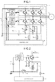
- FIG. 1 is a diagram illustrating a configuration example of a power conversion device according to a first embodiment of the present invention.
- a power conversion device 10 illustrated in FIG. 1 is located between a DC power supply 1 and a motor 3, and converts DC power of the DC power supply 1, which is to be supplied to the motor 3 (load), to three-phase AC power.
- the power conversion device 10 illustrated in FIG. 1 includes an inverter 2, a peripheral circuit unit 4a, a drive circuit unit 5, and a control unit 8.
- the inverter 2 includes a lower arm portion 21 and an upper arm portion 22, and is configured by three legs.
- the lower arm portion 21 includes switching elements 21a to 21c.
- the switching element 21a is a U-phase lower-arm switching element.
- the switching element 21b is a V-phase lower-arm switching element.
- the switching element 21c is a W-phase lower-arm switching element.
- the upper arm portion 22 includes switching elements 22a to 22c.
- the switching element 22a is a U-phase upper-arm switching element.
- the switching element 22b is a V-phase upper-arm switching element.
- the switching element 22c is a W-phase upper-arm switching element.
- the control unit 8 generates drive signals respectively for the switching elements 21a to 21c and 22a to 22c included in the inverter 2, and outputs the drive signals thereto.
- the control unit 8 is a controller that includes a microcomputer or a central processing unit (CPU) for example, and converts an input analog voltage signal (including a detection value) to a digital value to execute computation and control according to a control application of the motor 3.
- the drive circuit unit 5 includes a lower-arm gate drive circuit 51 and an upper-arm gate drive circuit 52.
- the lower-arm gate drive circuit 51 applies, according to drive signals generated and output by the control unit 8, a drive voltage to respective gate terminals of the switching elements 21a to 21c.
- the upper-arm gate drive circuit 52 applies, according to drive signals generated and output by the control unit 8, a drive voltage to respective gate terminals of the switching elements 22a to 22c.
- Reflux diodes 41a to 41c and 42a to 42c are connected to the switching elements 21a to 21c and 22a to 22c, respectively, in inverse parallel.
- the peripheral circuit unit 4a includes a power-supply shunt resistance 6, lower-arm shunt resistances 7a and 7b, and lower-arm voltage detection units 9a and 9b.
- the power-supply shunt resistance 6 is provided between the inverter 2 and the negative-voltage (GND) side of the DC power supply 1.
- the resistance value of the power-supply shunt resistance 6 is represented as R dc .
- the lower-arm shunt resistances 7a and 7b are provided between the power-supply shunt resistance 6 and emitters of the respective switching elements 21a and 21b in the lower arm portion 21.
- the lower-arm shunt resistance 7a is a U-phase lower-arm shunt resistance.
- the lower-arm shunt resistance 7b is a V-phase lower-arm shunt resistance.
- the resistance value of the respective lower-arm shunt resistances 7a and 7b is represented as R sh .
- the lower-arm voltage detection unit 9a is provided between the control unit 8 and a connection point between the lower-arm shunt resistance 7a and the emitter of the switching element 21a in the lower arm portion 21.
- the lower-arm voltage detection unit 9b is provided between the control unit 8 and a connection point between the lower-arm shunt resistance 7b and the emitter of the switching element 21b in the lower arm portion 21.
- the lower-arm voltage detection unit 9a is a U-phase lower-arm voltage detection unit.
- the lower-arm voltage detection unit 9b is a V-phase lower-arm voltage detection unit.
- the lower-arm voltage detection unit 9a detects a voltage (V u ) between the negative-voltage (GND) side of the DC power supply 1 and the connection point between the lower-arm shunt resistance 7a and the emitter of the switching element 21a in the lower arm portion 21.
- the lower-arm voltage detection unit 9b detects a voltage (V v ) between the negative-voltage (GND) side of the DC power supply 1 and the connection point between the lower-arm shunt resistance 7b and the emitter of the switching element 21b in the lower arm portion 21.
- Each of the lower-arm voltage detection units 9a and 9b is configured by, for example, an amplification unit that is capable of setting the voltages V u and V v to voltage values that are easily processed by the control unit 8.
- the control unit 8 calculates a motor current according to voltage values detected by the lower-arm voltage detection units 9a and 9b, and performs control computation, and in accordance with the calculated current value, the control unit 8 generates a drive signal.
- FIG. 2 is a diagram illustrating a portion of the peripheral circuit unit 4a, which is connected to the switching element 21a (the U-phase lower-arm switching element), extracting the region surrounded by the dotted line in FIG. 1 .
- a lower-arm gate drive circuit 51a that is a part of the lower-arm gate drive circuit 51 is connected to the gate terminal of the switching element 21a.
- the positive-voltage side (the positive side) of a DC power supply 11 is connected to the lower-arm gate drive circuit 51a.
- the lower-arm gate drive circuit 51a changes over the voltage to be applied to the gate terminal of the switching element 21a. That is, when the switching element 21a is to be turned on, a voltage (V cc ) that is higher than a threshold voltage V th of the switching element 21a is applied to the gate terminal of the switching element 21a.
- V E V Rsh_u + V Rdc
- the above expression (6) is the condition for the switching element 21a to maintain an on-state.
- FIGS. 3 are schematic diagrams illustrating an example of a switching waveform (A) of the gate terminal potential V G , and switching waveforms (B and C) of the gate-emitter voltage V GE in the power conversion device 10 according to the present embodiment of the invention.
- the gate terminal potential V G becomes V cc when the switching element 21a is turned on, and becomes 0 V when the switching element 21a is turned off, according to a drive signal from the control unit 8. Therefore, the waveform of the gate terminal potential V G is a rectangular wave ( FIG. 3(A) ).
- the waveform of the gate-emitter voltage V GE is also a rectangular wave, however, it is offset in the negative direction by the amount of the emitter terminal potential V E .
- the switching element 21a can be driven stably.
- each of the lower-arm voltage detection units 9a and 9b is configured by an amplification unit that sets the voltage value to a voltage that is easily processed by the control unit 8.
- Examples of such an amplification unit include an operational amplifier.
- an operational amplifier generally has a dead zone, when an operational amplifier is used as an amplification unit, an input voltage of the operational amplifier is adjusted to be equal to or greater than the voltage in the dead zone.
- a power conversion device that includes shunt resistances and switching elements and that is capable of executing stable control can be obtained.
- the power conversion device 10 of the present embodiment can have a configuration in which an overcurrent is detected.
- the resistance value of the shunt resistance is set according to an on-voltage of the switching element. Therefore, the resistance value is reduced and the current value can be increased. Accordingly, the configuration of detecting an overcurrent is effective.
- the control unit 8 can include a current calculation unit and a comparison unit.
- the current calculation unit uses a voltage value detected in the manner as described above and a resistance value of the shunt resistance to calculate a current value and output the calculated current value to the comparison unit.
- the comparison unit includes a storage unit.
- the storage unit has an overcurrent threshold for overcurrent determination stored therein.
- the comparison unit compares the calculated current value with the overcurrent threshold. It can be configured such that, when the calculated current value is equal to or greater than the overcurrent threshold or the calculated current value exceeds the overcurrent threshold, the control unit 8 stops generating a drive signal and stops applying a drive voltage V cc to the switching element.
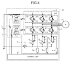
- FIG. 4 is a diagram illustrating a configuration example of a power conversion device according to a second embodiment of the present invention.
- a power conversion device 20 illustrated in FIG. 4 is located between the DC power supply 1 and the motor 3, and converts DC power of the DC power supply 1 to be supplied to the motor 3 (load) to three-phase AC power.
- the power conversion device 20 illustrated in FIG. 4 includes the inverter 2, a peripheral circuit unit 4b, the drive circuit unit 5, and the control unit 8.
- the inverter 2, the drive circuit unit 5, and the control unit 8 are identical to those described in the first embodiment.
- the peripheral circuit unit 4b includes the power-supply shunt resistance 6, the lower-arm shunt resistances 7a and 7b and a lower-arm shunt resistance 7c, and the lower-arm voltage detection units 9a and 9b and a lower-arm voltage detection unit 9c. That is, the power conversion device 20 is different from the power conversion device 10 illustrated in FIG. 1 according to the first embodiment in that the power conversion device 20 includes the lower-arm shunt resistance 7c and the lower-arm voltage detection unit 9c. Other configurations are identical to those of the power conversion device 10 according to the first embodiment. Therefore, the descriptions thereof in the first embodiment are cited.
- the lower-arm shunt resistance 7c is provided between the power-supply shunt resistance 6 and an emitter of the switching element 21c in the lower arm portion 21.
- the lower-arm shunt resistance 7c is a W-phase lower-arm shunt resistance.
- the resistance value of the lower-arm shunt resistance 7c is represented as R sh .
- the lower-arm voltage detection unit 9c is provided between the control unit 8 and a connection point between the lower-arm shunt resistance 7c with an emitter of the switching element 21c in the lower arm portion 21.
- the lower-arm voltage detection unit 9c is a W-phase lower-arm voltage detection unit.
- the lower-arm voltage detection unit 9c detects a voltage (V w ) between the negative-voltage (GND) side of the DC power supply 1 and the connection point between the lower-arm shunt resistance 7c and the emitter of the switching element 21c in the lower arm portion 21.
- the lower-arm voltage detection unit 9c is configured by, for example, an amplification unit that is capable of setting the voltage V w to a voltage value that is easily processed by the control unit 8.
- the control unit 8 calculates a motor current according to a voltage value detected by the lower-arm voltage detection units 9a, 9b, and 9c, and performs control computation.
- the switching element 21a can be driven stably.
- a lower-arm shunt resistance and a lower-arm voltage detection unit can be provided to each of the three phases.
- the power conversion device 20 of the present embodiment can have a configuration in which an overcurrent is detected.
- FIG. 5 is a diagram illustrating a configuration example of a power conversion device according to a third embodiment of the present invention.
- a power conversion device 30 illustrated in FIG. 5 is located between the DC power supply 1 and the motor 3, and converts DC power of the DC power supply 1 to be supplied to the motor 3 (load) to three-phase AC power.
- the power conversion device 30 illustrated in FIG. 5 includes the inverter 2, a peripheral circuit unit 4c, the drive circuit unit 5, and the control unit 8.
- the inverter 2, the drive circuit unit 5, and the control unit 8 are identical to those described in the first embodiment.
- the peripheral circuit unit 4c includes the power-supply shunt resistance 6 and a power-supply shunt-voltage detection unit 9. That is, the power conversion device 30 is different from the power conversion device 10 illustrated in FIG. 1 according to the first embodiment in that the power conversion device 30 includes neither the lower-arm shunt resistances 7a and 7b nor the lower-arm voltage detection units 9a, 9b, and 9c, but includes the power-supply shunt-voltage detection unit 9. Other configurations are identical to those of the power conversion device 10 according to the first embodiment. Therefore, the descriptions thereof in the first embodiment are cited.
- the power-supply shunt-voltage detection unit 9 is provided between the power-supply shunt resistance 6 and the emitters of the switching elements 21a to 21c in the lower arm portion 21, and detects the voltage (V Rdc ) between the negative-voltage (GND) side of the DC power supply 1 and the emitter-side of the switching elements 21a to 21c in the lower arm portion 21.
- the power-supply shunt-voltage detection unit 9 is configured by, for example, an amplification unit that is capable of setting the voltage V Rdc to a voltage value that is easily processed by the control unit 8.
- the control unit 8 calculates a motor current according to a voltage value detected by the power-supply shunt-voltage detection unit 9, and performs control computation.
- FIG. 6 is a diagram illustrating a portion of the peripheral circuit unit 4c, which is connected to the switching element 21a (the U-phase lower-arm switching element), extracting the region surrounded by the dotted line in FIG. 5 and corresponding to FIG. 2 according to the first embodiment.
- the lower-arm gate drive circuit 51a that is a part of the lower-arm gate drive circuit 51 is connected to the gate terminal of the switching element 21a.
- the positive-voltage side of the DC power supply 11 is connected to the gate drive circuit 51a.
- the lower-arm gate drive circuit 51a changes over the voltage to be applied to the gate terminal of the switching element 21a. That is, when the switching element 21a is to be turned on, a voltage (V cc ) that is higher than the threshold voltage V th of the switching element 21a is applied to the gate terminal of the switching element 21a.
- the gate-emitter voltage V GE in the switching element 21a is expressed as the expression (1) in the first embodiment by using the emitter terminal potential V E and the gate terminal potential V G relative to the reference potential (GND) of the lower-arm gate drive circuit 51a.
- the potential V cc on the positive-voltage side of the DC power supply 11 relative to the reference potential (GND) is a fixed value. Therefore, the gate-emitter voltage V GE in the switching element 21a is varied according to the voltage V Rdc across the power-supply shunt resistance 6.
- the above expression (11) is the condition for the switching element 21a to maintain the on-state.
- the gate terminal potential V G becomes V cc when the switching element 21a is turned on and becomes 0 V when the switching element 21a is turned off, according to a drive signal from the control unit 8. Therefore, the waveform of the gate terminal potential V G is a rectangular wave.
- the waveform of the gate-emitter voltage V GE is also a rectangular wave, however, it is offset in the negative direction by the amount of the emitter terminal potential V E (the voltage V Rdc ).
- the gate-emitter voltage V GE when the switching element 21a is on becomes lower than the threshold voltage V th . Therefore, the switching element 21a is turned off.
- the gate-emitter voltage V GE when the switching element 21a is on does not become lower than the threshold voltage V th even with the offset amount taken into account. Therefore, the switching element 21a maintains the on-state.
- the switching element 21a can be driven stably.
- examples of the amplification unit that constitutes the power-supply shunt-voltage detection unit 9 include an operational amplifier. Since an operational amplifier generally has a dead zone, when an operational amplifier is used as an amplification unit, an input voltage of the operational amplifier is adjusted to be equal to or greater than the voltage in the dead zone.
- the power conversion device does not include a lower-arm shunt resistance or a lower-arm voltage detection unit, by including a power-supply shunt resistance and a power-supply shunt-voltage detection unit, a power conversion device that includes a shunt resistance and a switching element and that is capable of executing stable control can be obtained.
- the number of elements can be reduced as compared to the first and second embodiments.
- the power conversion device 30 of the present embodiment can have a configuration in which an overcurrent is detected, it can be configured such that an overcurrent detection unit 12 illustrated in FIG. 6 directly uses a shunt-resistance potential to perform overcurrent detection by means of hardware.
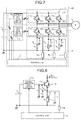
- FIG. 7 is a diagram illustrating a configuration example of a power conversion device according to a fourth embodiment of the present invention.
- a power conversion device 40 illustrated in FIG. 7 is located between the DC power supply 1 and the motor 3, and converts DC power of the DC power supply 1 to be supplied to the motor 3 (load) to three-phase AC power.
- the power conversion device 40 illustrated in FIG. 7 includes the inverter 2, a peripheral circuit unit 4d, the drive circuit unit 5, and the control unit 8.
- the inverter 2, the drive circuit unit 5, and the control unit 8 are identical to those described in the first embodiment.
- the peripheral circuit unit 4d includes the lower-arm shunt resistances 7a, 7b, and 7c, and the lower-arm voltage detection units 9a, 9b, and 9c. That is, the power conversion device 40 is different from the power conversion device 10 illustrated in FIG. 1 according to the first embodiment in that the power conversion device 40 does not include the power-supply shunt resistance 6, but includes the lower-arm shunt resistance 7c and the lower-arm voltage detection unit 9c. Other configurations are identical to those of the power conversion device 10 according to the first embodiment. Therefore, the descriptions thereof in the first embodiment are cited. The power conversion device 40 is different from the power conversion device 20 illustrated in FIG. 4 according to the second embodiment in that the power conversion device 40 does not include the power-supply shunt resistance 6.
- the lower-arm shunt resistances 7a, 7b, and 7c are provided between the negative-voltage side (the GND side) of the DC power supply 1 and respective emitters of the switching elements 21a, 21b, and 21c in the lower arm portion 21.
- the lower-arm shunt resistance 7a is a U-phase lower-arm shunt resistance.
- the lower-arm shunt resistance 7b is a V-phase lower-arm shunt resistance.
- the lower-arm shunt resistance 7c is a W-phase lower-arm shunt resistance.
- the resistance value of the respective lower-arm shunt resistances 7a, 7b, and 7c is represented as R sh .
- the lower-arm voltage detection unit 9a is provided between the control unit 8 and the connection point between the lower-arm shunt resistance 7a and the emitter of the switching element 21a in the lower arm portion 21.
- the lower-arm voltage detection unit 9b is provided between the control unit 8 and the connection point between the lower-arm shunt resistance 7b and the emitter of the switching element 21b in the lower arm portion 21.
- the lower-arm voltage detection unit 9c is provided between the control unit 8 and the connection point between the lower-arm shunt resistance 7c and the emitter of the switching element 21c in the lower arm portion 21.
- the lower-arm voltage detection unit 9a is a U-phase lower-arm voltage detection unit.
- the lower-arm voltage detection unit 9b is a V-phase lower-arm voltage detection unit.
- the lower-arm voltage detection unit 9c is a W-phase lower-arm voltage detection unit.
- the lower-arm voltage detection unit 9a detects a voltage (V u ) between the negative-voltage (GND) side of the DC power supply 1 and the connection point between the lower-arm shunt resistance 7a and the emitter of the switching element 21a in the lower arm portion 21.
- the lower-arm voltage detection unit 9b detects a voltage (V v ) between the negative-voltage (GND) side of the DC power supply 1 and the connection point between the lower-arm shunt resistance 7b and the emitter of the switching element 21b in the lower arm portion 21.
- the lower-arm voltage detection unit 9c detects a voltage (V w ) between the negative-voltage (GND) side of the DC power supply 1 and the connection point between the lower-arm shunt resistance 7c and the emitter of the switching element 21c in the lower arm portion 21.
- Each of the lower-arm voltage detection units 9a, 9b, and 9c is configured by, for example, an amplification unit that is capable of setting the voltages V u , V v , and V w to voltage values that are easily processed by the control unit 8.
- the control unit 8 calculates a motor current according to a voltage value detected by the lower-arm voltage detection units 9a, 9b, and 9c, and performs control computation.
- FIG. 8 is a diagram illustrating a portion of the peripheral circuit unit 4d, which is connected to the switching element 21a (the U-phase lower-arm switching element), extracting the region surrounded by the dotted line in FIG. 7 and corresponding to FIG. 2 according to the first embodiment, or corresponding to FIG. 6 according to the third embodiment.
- the lower-arm gate drive circuit 51a that is a part of the lower-arm gate drive circuit 51 is connected to the gate terminal of the switching element 21a.
- the positive-voltage side of the DC power supply 11 is connected to the lower-arm gate drive circuit 51a.
- the lower-arm gate drive circuit 51a changes over the voltage to be applied to the gate terminal of the switching element 21a. That is, when the switching element 21a is to be turned on, a voltage (V cc ) that is higher than the threshold voltage V th of the switching element 21a is applied to the gate terminal of the switching element 21a.
- the gate-emitter voltage V GE in the switching element 21a is expressed as the expression (1) in the first embodiment by using the emitter terminal potential V E and the gate terminal potential V G relative to the reference potential (GND) of the lower-arm gate drive circuit 51a.
- the potential V cc on the positive-voltage side of the DC power supply 11 relative to the reference potential (GND) is a fixed value. Therefore, the gate-emitter voltage V GE in the switching element 21a is varied according to the voltage V Rdc across the power-supply shunt resistance 6 and the voltage V Rsh_u across the lower-arm voltage detection unit 9a.
- the above expression (16) is the condition for the switching element 21a to maintain an on-state.
- the gate terminal potential V G becomes V cc when the switching element 21a is turned on and becomes 0 V when the switching element 21a is turned off, according to a drive signal from the control unit 8. Therefore, the waveform of the gate terminal potential V G is a rectangular wave.
- the waveform of the gate-emitter voltage V GE is also a rectangular wave, however, it is offset in the negative direction by the amount of the emitter terminal potential V E (the voltage V Rsh_u ).
- the gate-emitter voltage V GE when the switching element 21a is on becomes lower than the threshold voltage V th . Therefore, the switching element 21a is turned off.
- the gate-emitter voltage V GE when the switching element 21a is on does not become lower than the threshold voltage V th even with the offset amount taken into account. Therefore, the switching element 21a maintains the on-state.
- the switching element 21a can be driven stably.
- examples of the amplification unit that constitutes each of the lower-arm voltage detection units 9a, 9b, and 9c include an operational amplifier. Since an operational amplifier generally has a dead zone, when an operational amplifier is used as an amplification unit, an input voltage of the operational amplifier is adjusted to be equal to or greater than the voltage in the dead zone.
- the power conversion device does not include a power-supply shunt resistance, by including lower-arm shunt resistances and lower-arm voltage detection units corresponding to all the phases, a power conversion device that includes a shunt resistance and a switching element and that is capable of executing stable control can be obtained.
- the power conversion device 30 of the present embodiment may have a configuration of detecting an overcurrent.
- FIG. 9 is a diagram illustrating a configuration example of a power conversion device according to a fifth embodiment of the present invention.
- a power conversion device 50 illustrated in FIG. 9 is located between an AC power supply 501 and a load 503.
- the power conversion device 50 converts AC power supplied from the AC power supply 501 to DC power, and boosts the voltage of this DC power to be supplied to the load 503.
- the power conversion device 50 illustrated in FIG. 9 includes a rectifying circuit 502, a smoothing capacitor 504, a reactor 505, a backflow prevention diode 506, a switching element 507, a control unit 508, and a gate drive circuit 509.
- the rectifying circuit 502 converts AC power supplied from the AC power supply 501 to DC power.
- the smoothing capacitor 504 smooths a DC voltage output from the rectifying circuit 502.
- the reactor 505 is connected to the positive-voltage side of the smoothing capacitor 504.
- the backflow prevention diode 506 prevents backflow of a current from the load 503.
- the switching element 507 executes short-circuit control.
- the control unit 508 generates a drive signal for the switching element 507 and outputs the drive signal.
- the control unit 508 is a controller that is configured by a microcomputer or a CPU for example, and converts an input analog voltage signal to a digital value to control the voltage or the current to be supplied to the load 503. According to a drive signal output from the control unit 508, the gate drive circuit 509 applies a drive voltage to a gate terminal of the switching element 507.
- the power conversion device 50 illustrated in FIG. 9 further includes a shunt resistance 510 and a shunt-resistance voltage detection unit 511.
- the shunt resistance 510 is provided between an emitter terminal of the switching element 507 and the negative-voltage side of the AC power supply 501.
- the shunt-resistance voltage detection unit 511 is provided between the negative-voltage side of the AC power supply 501 and a connection point between the shunt resistance 510 and the switching element 507.
- the resistance value of the shunt resistance 510 is represented as R sh .
- the shunt-resistance voltage detection unit 511 is configured by, for example, an amplification unit that is capable of setting a voltage V 0 of the shunt resistance 510 to a voltage value that is easily processed by the control unit 508.
- the control unit 508 controls the voltage and the current to be supplied to the load 503, according to a voltage value detected by the shunt-resistance voltage detection unit 511.
- FIG. 10 is a diagram illustrating a portion of the peripheral circuit unit of the power conversion device 50, which is connected to the switching element 507, extracting the region surrounded by the dotted line in FIG. 9 .
- a gate drive circuit 509 that is a part of the gate drive circuit 509 is connected to the gate terminal of the switching element 507.
- the positive-voltage side of a DC power supply 512 is connected to the gate drive circuit 509.
- the gate drive circuit 509 changes over the voltage to be applied to the gate terminal of the switching element 507. That is, when the switching element 507 is to be turned on, a voltage (V cc ) that is higher than a threshold voltage V th of the switching element 507 is applied to the gate terminal of the switching element 507.
- the gate-emitter voltage V GE in the switching element 507 is expressed as the expression (1) in the first embodiment by using the emitter terminal potential V E and the gate terminal potential V G relative to the reference potential (GND) of the gate drive circuit 509.
- the potential V cc on the positive-voltage side of the DC power supply 11 relative to the reference potential (GND) is a fixed value. Therefore, the gate-emitter voltage V GE in the switching element 507 is varied according to the voltage V Rdc across the shunt resistance 510.
- the gate terminal potential V G becomes V cc when the switching element 21a is turned on and becomes 0 V when the switching element 21a is turned off, according to a drive signal from the control unit 8. Therefore, the waveform of the gate terminal potential V G is a rectangular wave.
- the waveform of the gate-emitter voltage V GE is also a rectangular wave, however, it is offset in the negative direction by the amount of the emitter terminal potential V E (the voltage V Rsh_u ).
- the gate-emitter voltage V GE when the switching element 21a is on becomes lower than the threshold voltage V th . Therefore, the switching element 21a is turned off.
- the gate-emitter voltage V GE when the switching element 21a is on does not become lower than the threshold voltage V th even with the offset amount taken into account. Therefore, the switching element 21a maintains an on-state.
- the switching element 507 can be driven stably.
- examples of the amplification unit that constitutes the shunt-resistance voltage detection unit 511 include an operational amplifier. Since an operational amplifier generally has a dead zone, when an operational amplifier is used as an amplification unit, an input voltage of the operational amplifier is adjusted to be equal to or greater than the voltage within the dead zone.
- a power conversion device that includes a shunt resistance and a switching element and that is capable of executing stable control can be obtained.
- the present invention is not limited thereto.
- the present invention can be also configured such that the power conversion device converts DC power of the DC power supply 1 to single-phase AC power.
- the power conversion device described in the first to fifth embodiments has exemplified a motor as a load, and therefore the motor can be applied to a motor drive device in the above manner.
- a motor drive device can be applied to an air blower or a compressor installed in an air conditioner, a refrigerator, or a freezer.
Landscapes
- Engineering & Computer Science (AREA)
- Power Engineering (AREA)
- Inverter Devices (AREA)
- Dc-Dc Converters (AREA)
- Power Conversion In General (AREA)
Applications Claiming Priority (1)
| Application Number | Priority Date | Filing Date | Title |
|---|---|---|---|
| PCT/JP2013/075919 WO2015045035A1 (ja) | 2013-09-25 | 2013-09-25 | 開閉装置、電力変換装置、モータ駆動装置、送風機、圧縮機、空気調和機、冷蔵庫及び冷凍機 |
Publications (3)
| Publication Number | Publication Date |
|---|---|
| EP3051676A1 true EP3051676A1 (de) | 2016-08-03 |
| EP3051676A4 EP3051676A4 (de) | 2017-03-29 |
| EP3051676B1 EP3051676B1 (de) | 2018-08-29 |
Family
ID=52742242
Family Applications (1)
| Application Number | Title | Priority Date | Filing Date |
|---|---|---|---|
| EP13894471.5A Active EP3051676B1 (de) | 2013-09-25 | 2013-09-25 | Schaltvorrichtung, stromumwandlungsvorrichtung, und motorantriebsvorrichtung. |
Country Status (8)
| Country | Link |
|---|---|
| US (1) | US9960702B2 (de) |
| EP (1) | EP3051676B1 (de) |
| JP (1) | JPWO2015045035A1 (de) |
| CN (1) | CN105531915B (de) |
| ES (1) | ES2690329T3 (de) |
| RU (1) | RU2632916C1 (de) |
| TR (1) | TR201814652T4 (de) |
| WO (1) | WO2015045035A1 (de) |
Families Citing this family (6)
| Publication number | Priority date | Publication date | Assignee | Title |
|---|---|---|---|---|
| JP6988517B2 (ja) * | 2018-01-25 | 2022-01-05 | トヨタ自動車株式会社 | 電力変換装置 |
| JP2020061903A (ja) * | 2018-10-12 | 2020-04-16 | 株式会社デンソー | ゲート駆動装置 |
| JP7132099B2 (ja) * | 2018-11-20 | 2022-09-06 | 株式会社日立インダストリアルプロダクツ | 電力変換装置 |
| JP7151605B2 (ja) * | 2019-04-16 | 2022-10-12 | 株式会社デンソー | 電力変換器 |
| US11831249B2 (en) * | 2019-11-06 | 2023-11-28 | Toshiba Mitsubishi-Electric Industrial Systems Corporation | Power conversion apparatus |
| JP7292196B2 (ja) * | 2019-12-16 | 2023-06-16 | 三菱電機株式会社 | 駆動装置およびパワーモジュール |
Family Cites Families (24)
| Publication number | Priority date | Publication date | Assignee | Title |
|---|---|---|---|---|
| SU1410212A2 (ru) * | 1986-12-19 | 1988-07-15 | Всесоюзный Научно-Исследовательский,Проектно-Конструкторский И Технологический Институт Релестроения | Управл емый вентильный электродвигатель |
| JP2720980B2 (ja) | 1987-08-28 | 1998-03-04 | 藤井電機工業株式会社 | 放電灯用点灯装置 |
| US5532617A (en) * | 1994-03-25 | 1996-07-02 | Philips Electronics North America Corporation | CMOS input with temperature and VCC compensated threshold |
| DE19802604A1 (de) * | 1997-01-27 | 1998-08-06 | Int Rectifier Corp | Motor-Steuergeräteschaltung |
| JP2001136788A (ja) * | 1999-11-08 | 2001-05-18 | Nippon Densan Corp | モータ駆動装置 |
| JP3854190B2 (ja) * | 2002-04-26 | 2006-12-06 | 株式会社ジェイテクト | モータ制御装置 |
| WO2006009145A1 (ja) | 2004-07-20 | 2006-01-26 | Matsushita Electric Industrial Co., Ltd. | インバータ装置 |
| CN100568699C (zh) * | 2004-07-20 | 2009-12-09 | 松下电器产业株式会社 | 变换器装置 |
| ES2624929T3 (es) * | 2004-08-27 | 2017-07-18 | Mitsubishi Denki Kabushiki Kaisha | Generador de señal PWM de tres fases |
| JP4539237B2 (ja) | 2004-08-30 | 2010-09-08 | パナソニック株式会社 | インバータ装置 |
| JP4492397B2 (ja) * | 2005-03-14 | 2010-06-30 | 株式会社デンソー | 三相電圧型インバータ装置 |
| JP2006271048A (ja) | 2005-03-23 | 2006-10-05 | Matsushita Electric Ind Co Ltd | モータ駆動装置 |
| RU2343622C1 (ru) * | 2007-11-09 | 2009-01-10 | Альберт Герасимович Алексеев | Способ управления транзисторным ключом на тиристоре и устройство для его осуществления |
| JP5446324B2 (ja) * | 2008-03-12 | 2014-03-19 | 三洋電機株式会社 | インバータ装置 |
| JP5142917B2 (ja) * | 2008-09-26 | 2013-02-13 | オムロンオートモーティブエレクトロニクス株式会社 | 多相モータ駆動装置 |
| JP5289565B2 (ja) * | 2009-05-19 | 2013-09-11 | 三菱電機株式会社 | ゲート駆動回路 |
| AU2010299394B2 (en) * | 2009-09-28 | 2014-02-27 | Daikin Industries, Ltd. | Phase current detection device and power conversion device using same |
| JP5029678B2 (ja) * | 2009-12-07 | 2012-09-19 | 株式会社デンソー | スイッチング素子の駆動装置 |
| JP5544873B2 (ja) * | 2009-12-25 | 2014-07-09 | 株式会社デンソー | スイッチング素子の駆動装置 |
| JP5489798B2 (ja) | 2010-03-17 | 2014-05-14 | 三菱電機株式会社 | 電流検出装置およびモータシステム |
| JP5655367B2 (ja) | 2010-05-07 | 2015-01-21 | パナソニックIpマネジメント株式会社 | モータ駆動装置 |
| JP5348115B2 (ja) | 2010-11-22 | 2013-11-20 | 株式会社デンソー | 負荷駆動装置 |
| US9184739B2 (en) * | 2011-06-09 | 2015-11-10 | Mitsubishi Electric Corporation | Gate drive circuit |
| CN104871417B (zh) * | 2012-12-21 | 2018-03-06 | 三菱电机株式会社 | 开关元件驱动电路、功率模块以及汽车 |
-
2013
- 2013-09-25 TR TR2018/14652T patent/TR201814652T4/tr unknown
- 2013-09-25 US US15/022,577 patent/US9960702B2/en active Active
- 2013-09-25 CN CN201380079498.9A patent/CN105531915B/zh not_active Expired - Fee Related
- 2013-09-25 RU RU2016115521A patent/RU2632916C1/ru active
- 2013-09-25 JP JP2015538684A patent/JPWO2015045035A1/ja active Pending
- 2013-09-25 WO PCT/JP2013/075919 patent/WO2015045035A1/ja not_active Ceased
- 2013-09-25 EP EP13894471.5A patent/EP3051676B1/de active Active
- 2013-09-25 ES ES13894471.5T patent/ES2690329T3/es active Active
Also Published As
| Publication number | Publication date |
|---|---|
| JPWO2015045035A1 (ja) | 2017-03-02 |
| US20160233783A1 (en) | 2016-08-11 |
| US9960702B2 (en) | 2018-05-01 |
| EP3051676A4 (de) | 2017-03-29 |
| CN105531915A (zh) | 2016-04-27 |
| TR201814652T4 (tr) | 2018-11-21 |
| WO2015045035A1 (ja) | 2015-04-02 |
| RU2632916C1 (ru) | 2017-10-11 |
| ES2690329T3 (es) | 2018-11-20 |
| EP3051676B1 (de) | 2018-08-29 |
| CN105531915B (zh) | 2019-03-15 |
Similar Documents
| Publication | Publication Date | Title |
|---|---|---|
| CN112242831B (zh) | 栅极驱动器电路和检测逆变器支路中的短路事件的方法 | |
| US10439542B2 (en) | Electric power conversion device | |
| US10084383B2 (en) | Booster device and converter device | |
| EP3051676A1 (de) | Schaltvorrichtung, stromumwandlungsvorrichtung, motorantriebsvorrichtung, gebläse, verdichter, klimaanlage, kühlschrank und gefrierschrank | |
| EP2381567A1 (de) | Bidirektionaler schaltkreis und leistungsumwandler damit | |
| EP2528221A2 (de) | Aktiver Mehrphasen-Gleichrichter | |
| US10924024B2 (en) | Regenerative power conversion system with inverter and converter | |
| JP2015065742A (ja) | インバータ制御装置およびインバータ装置の制御方法 | |
| JP2016073052A (ja) | スイッチング制御装置 | |
| EP2903160A1 (de) | Stromversorgungsvorrichtung und Steuerungsverfahren der Stromversorgungsvorrichtung | |
| US11050358B2 (en) | Power module with built-in drive circuit | |
| JP6717380B2 (ja) | 半導体モジュール、及び半導体モジュールに使われるスイッチング素子のチップ設計方法 | |
| CN104247243B (zh) | 整流装置及整流系统 | |
| JP5824339B2 (ja) | 三相整流装置 | |
| US8760890B2 (en) | Current source inverter | |
| CN113711479B (zh) | 功率转换装置 | |
| KR101946369B1 (ko) | 전력 변환 장치 및 이를 포함하는 공기 조화기 | |
| EP4175164A1 (de) | Aufwärtswandlerzustandssteuerung | |
| EP4716086A1 (de) | Vorrichtung zur umwandlung elektrischer energie | |
| US12597852B2 (en) | Protecting a power inverter by sensing a phase node voltage | |
| US20250309754A1 (en) | Protecting a power inverter by sensing a phase node voltage | |
| KR20110009567U (ko) | 지능형 전력모듈을 이용한 엘리베이터 모터구동장치 |
Legal Events
| Date | Code | Title | Description |
|---|---|---|---|
| PUAI | Public reference made under article 153(3) epc to a published international application that has entered the european phase |
Free format text: ORIGINAL CODE: 0009012 |
|
| 17P | Request for examination filed |
Effective date: 20160421 |
|
| AK | Designated contracting states |
Kind code of ref document: A1 Designated state(s): AL AT BE BG CH CY CZ DE DK EE ES FI FR GB GR HR HU IE IS IT LI LT LU LV MC MK MT NL NO PL PT RO RS SE SI SK SM TR |
|
| AX | Request for extension of the european patent |
Extension state: BA ME |
|
| DAX | Request for extension of the european patent (deleted) | ||
| A4 | Supplementary search report drawn up and despatched |
Effective date: 20170223 |
|
| RIC1 | Information provided on ipc code assigned before grant |
Ipc: H02M 7/48 20070101ALI20170218BHEP Ipc: H02M 1/08 20060101AFI20170218BHEP |
|
| 17Q | First examination report despatched |
Effective date: 20170927 |
|
| GRAP | Despatch of communication of intention to grant a patent |
Free format text: ORIGINAL CODE: EPIDOSNIGR1 |
|
| INTG | Intention to grant announced |
Effective date: 20180308 |
|
| GRAS | Grant fee paid |
Free format text: ORIGINAL CODE: EPIDOSNIGR3 |
|
| GRAA | (expected) grant |
Free format text: ORIGINAL CODE: 0009210 |
|
| AK | Designated contracting states |
Kind code of ref document: B1 Designated state(s): AL AT BE BG CH CY CZ DE DK EE ES FI FR GB GR HR HU IE IS IT LI LT LU LV MC MK MT NL NO PL PT RO RS SE SI SK SM TR |
|
| REG | Reference to a national code |
Ref country code: GB Ref legal event code: FG4D |
|
| REG | Reference to a national code |
Ref country code: CH Ref legal event code: EP |
|
| REG | Reference to a national code |
Ref country code: AT Ref legal event code: REF Ref document number: 1036321 Country of ref document: AT Kind code of ref document: T Effective date: 20180915 |
|
| REG | Reference to a national code |
Ref country code: IE Ref legal event code: FG4D |
|
| REG | Reference to a national code |
Ref country code: DE Ref legal event code: R096 Ref document number: 602013042945 Country of ref document: DE |
|
| REG | Reference to a national code |
Ref country code: SE Ref legal event code: TRGR |
|
| REG | Reference to a national code |
Ref country code: FR Ref legal event code: PLFP Year of fee payment: 6 |
|
| REG | Reference to a national code |
Ref country code: ES Ref legal event code: FG2A Ref document number: 2690329 Country of ref document: ES Kind code of ref document: T3 Effective date: 20181120 |
|
| REG | Reference to a national code |
Ref country code: NL Ref legal event code: MP Effective date: 20180829 |
|
| REG | Reference to a national code |
Ref country code: LT Ref legal event code: MG4D |
|
| PG25 | Lapsed in a contracting state [announced via postgrant information from national office to epo] |
Ref country code: BG Free format text: LAPSE BECAUSE OF FAILURE TO SUBMIT A TRANSLATION OF THE DESCRIPTION OR TO PAY THE FEE WITHIN THE PRESCRIBED TIME-LIMIT Effective date: 20181129 Ref country code: NL Free format text: LAPSE BECAUSE OF FAILURE TO SUBMIT A TRANSLATION OF THE DESCRIPTION OR TO PAY THE FEE WITHIN THE PRESCRIBED TIME-LIMIT Effective date: 20180829 Ref country code: LT Free format text: LAPSE BECAUSE OF FAILURE TO SUBMIT A TRANSLATION OF THE DESCRIPTION OR TO PAY THE FEE WITHIN THE PRESCRIBED TIME-LIMIT Effective date: 20180829 Ref country code: GR Free format text: LAPSE BECAUSE OF FAILURE TO SUBMIT A TRANSLATION OF THE DESCRIPTION OR TO PAY THE FEE WITHIN THE PRESCRIBED TIME-LIMIT Effective date: 20181130 Ref country code: FI Free format text: LAPSE BECAUSE OF FAILURE TO SUBMIT A TRANSLATION OF THE DESCRIPTION OR TO PAY THE FEE WITHIN THE PRESCRIBED TIME-LIMIT Effective date: 20180829 Ref country code: IS Free format text: LAPSE BECAUSE OF FAILURE TO SUBMIT A TRANSLATION OF THE DESCRIPTION OR TO PAY THE FEE WITHIN THE PRESCRIBED TIME-LIMIT Effective date: 20181229 Ref country code: RS Free format text: LAPSE BECAUSE OF FAILURE TO SUBMIT A TRANSLATION OF THE DESCRIPTION OR TO PAY THE FEE WITHIN THE PRESCRIBED TIME-LIMIT Effective date: 20180829 Ref country code: NO Free format text: LAPSE BECAUSE OF FAILURE TO SUBMIT A TRANSLATION OF THE DESCRIPTION OR TO PAY THE FEE WITHIN THE PRESCRIBED TIME-LIMIT Effective date: 20181129 |
|
| REG | Reference to a national code |
Ref country code: AT Ref legal event code: MK05 Ref document number: 1036321 Country of ref document: AT Kind code of ref document: T Effective date: 20180829 |
|
| PG25 | Lapsed in a contracting state [announced via postgrant information from national office to epo] |
Ref country code: LV Free format text: LAPSE BECAUSE OF FAILURE TO SUBMIT A TRANSLATION OF THE DESCRIPTION OR TO PAY THE FEE WITHIN THE PRESCRIBED TIME-LIMIT Effective date: 20180829 Ref country code: HR Free format text: LAPSE BECAUSE OF FAILURE TO SUBMIT A TRANSLATION OF THE DESCRIPTION OR TO PAY THE FEE WITHIN THE PRESCRIBED TIME-LIMIT Effective date: 20180829 Ref country code: AL Free format text: LAPSE BECAUSE OF FAILURE TO SUBMIT A TRANSLATION OF THE DESCRIPTION OR TO PAY THE FEE WITHIN THE PRESCRIBED TIME-LIMIT Effective date: 20180829 |
|
| PG25 | Lapsed in a contracting state [announced via postgrant information from national office to epo] |
Ref country code: RO Free format text: LAPSE BECAUSE OF FAILURE TO SUBMIT A TRANSLATION OF THE DESCRIPTION OR TO PAY THE FEE WITHIN THE PRESCRIBED TIME-LIMIT Effective date: 20180829 Ref country code: CZ Free format text: LAPSE BECAUSE OF FAILURE TO SUBMIT A TRANSLATION OF THE DESCRIPTION OR TO PAY THE FEE WITHIN THE PRESCRIBED TIME-LIMIT Effective date: 20180829 Ref country code: EE Free format text: LAPSE BECAUSE OF FAILURE TO SUBMIT A TRANSLATION OF THE DESCRIPTION OR TO PAY THE FEE WITHIN THE PRESCRIBED TIME-LIMIT Effective date: 20180829 Ref country code: AT Free format text: LAPSE BECAUSE OF FAILURE TO SUBMIT A TRANSLATION OF THE DESCRIPTION OR TO PAY THE FEE WITHIN THE PRESCRIBED TIME-LIMIT Effective date: 20180829 Ref country code: PL Free format text: LAPSE BECAUSE OF FAILURE TO SUBMIT A TRANSLATION OF THE DESCRIPTION OR TO PAY THE FEE WITHIN THE PRESCRIBED TIME-LIMIT Effective date: 20180829 |
|
| REG | Reference to a national code |
Ref country code: CH Ref legal event code: PL |
|
| PG25 | Lapsed in a contracting state [announced via postgrant information from national office to epo] |
Ref country code: SK Free format text: LAPSE BECAUSE OF FAILURE TO SUBMIT A TRANSLATION OF THE DESCRIPTION OR TO PAY THE FEE WITHIN THE PRESCRIBED TIME-LIMIT Effective date: 20180829 Ref country code: DK Free format text: LAPSE BECAUSE OF FAILURE TO SUBMIT A TRANSLATION OF THE DESCRIPTION OR TO PAY THE FEE WITHIN THE PRESCRIBED TIME-LIMIT Effective date: 20180829 Ref country code: SM Free format text: LAPSE BECAUSE OF FAILURE TO SUBMIT A TRANSLATION OF THE DESCRIPTION OR TO PAY THE FEE WITHIN THE PRESCRIBED TIME-LIMIT Effective date: 20180829 |
|
| REG | Reference to a national code |
Ref country code: DE Ref legal event code: R097 Ref document number: 602013042945 Country of ref document: DE |
|
| REG | Reference to a national code |
Ref country code: BE Ref legal event code: MM Effective date: 20180930 |
|
| REG | Reference to a national code |
Ref country code: IE Ref legal event code: MM4A |
|
| PG25 | Lapsed in a contracting state [announced via postgrant information from national office to epo] |
Ref country code: MC Free format text: LAPSE BECAUSE OF FAILURE TO SUBMIT A TRANSLATION OF THE DESCRIPTION OR TO PAY THE FEE WITHIN THE PRESCRIBED TIME-LIMIT Effective date: 20180829 Ref country code: LU Free format text: LAPSE BECAUSE OF NON-PAYMENT OF DUE FEES Effective date: 20180925 |
|
| PLBE | No opposition filed within time limit |
Free format text: ORIGINAL CODE: 0009261 |
|
| STAA | Information on the status of an ep patent application or granted ep patent |
Free format text: STATUS: NO OPPOSITION FILED WITHIN TIME LIMIT |
|
| PG25 | Lapsed in a contracting state [announced via postgrant information from national office to epo] |
Ref country code: IE Free format text: LAPSE BECAUSE OF NON-PAYMENT OF DUE FEES Effective date: 20180925 |
|
| 26N | No opposition filed |
Effective date: 20190531 |
|
| PG25 | Lapsed in a contracting state [announced via postgrant information from national office to epo] |
Ref country code: LI Free format text: LAPSE BECAUSE OF NON-PAYMENT OF DUE FEES Effective date: 20180930 Ref country code: CH Free format text: LAPSE BECAUSE OF NON-PAYMENT OF DUE FEES Effective date: 20180930 Ref country code: BE Free format text: LAPSE BECAUSE OF NON-PAYMENT OF DUE FEES Effective date: 20180930 Ref country code: SI Free format text: LAPSE BECAUSE OF FAILURE TO SUBMIT A TRANSLATION OF THE DESCRIPTION OR TO PAY THE FEE WITHIN THE PRESCRIBED TIME-LIMIT Effective date: 20180829 |
|
| PG25 | Lapsed in a contracting state [announced via postgrant information from national office to epo] |
Ref country code: MT Free format text: LAPSE BECAUSE OF NON-PAYMENT OF DUE FEES Effective date: 20180925 |
|
| PG25 | Lapsed in a contracting state [announced via postgrant information from national office to epo] |
Ref country code: PT Free format text: LAPSE BECAUSE OF FAILURE TO SUBMIT A TRANSLATION OF THE DESCRIPTION OR TO PAY THE FEE WITHIN THE PRESCRIBED TIME-LIMIT Effective date: 20180829 |
|
| PG25 | Lapsed in a contracting state [announced via postgrant information from national office to epo] |
Ref country code: HU Free format text: LAPSE BECAUSE OF FAILURE TO SUBMIT A TRANSLATION OF THE DESCRIPTION OR TO PAY THE FEE WITHIN THE PRESCRIBED TIME-LIMIT; INVALID AB INITIO Effective date: 20130925 Ref country code: MK Free format text: LAPSE BECAUSE OF NON-PAYMENT OF DUE FEES Effective date: 20180829 Ref country code: CY Free format text: LAPSE BECAUSE OF FAILURE TO SUBMIT A TRANSLATION OF THE DESCRIPTION OR TO PAY THE FEE WITHIN THE PRESCRIBED TIME-LIMIT Effective date: 20180829 |
|
| P01 | Opt-out of the competence of the unified patent court (upc) registered |
Effective date: 20230512 |
|
| REG | Reference to a national code |
Ref country code: DE Ref legal event code: R084 Ref document number: 602013042945 Country of ref document: DE |
|
| PGFP | Annual fee paid to national office [announced via postgrant information from national office to epo] |
Ref country code: TR Payment date: 20230922 Year of fee payment: 11 Ref country code: IT Payment date: 20230810 Year of fee payment: 11 Ref country code: GB Payment date: 20230803 Year of fee payment: 11 |
|
| PGFP | Annual fee paid to national office [announced via postgrant information from national office to epo] |
Ref country code: SE Payment date: 20230810 Year of fee payment: 11 Ref country code: FR Payment date: 20230808 Year of fee payment: 11 Ref country code: DE Payment date: 20230802 Year of fee payment: 11 |
|
| PGFP | Annual fee paid to national office [announced via postgrant information from national office to epo] |
Ref country code: ES Payment date: 20231003 Year of fee payment: 11 |
|
| REG | Reference to a national code |
Ref country code: GB Ref legal event code: 746 Effective date: 20240327 |
|
| REG | Reference to a national code |
Ref country code: ES Ref legal event code: GC2A Effective date: 20240412 |
|
| REG | Reference to a national code |
Ref country code: DE Ref legal event code: R119 Ref document number: 602013042945 Country of ref document: DE |
|
| REG | Reference to a national code |
Ref country code: SE Ref legal event code: EUG |
|
| GBPC | Gb: european patent ceased through non-payment of renewal fee |
Effective date: 20240925 |
|
| PG25 | Lapsed in a contracting state [announced via postgrant information from national office to epo] |
Ref country code: DE Free format text: LAPSE BECAUSE OF NON-PAYMENT OF DUE FEES Effective date: 20250401 |
|
| PG25 | Lapsed in a contracting state [announced via postgrant information from national office to epo] |
Ref country code: GB Free format text: LAPSE BECAUSE OF NON-PAYMENT OF DUE FEES Effective date: 20240925 |
|
| PG25 | Lapsed in a contracting state [announced via postgrant information from national office to epo] |
Ref country code: IT Free format text: LAPSE BECAUSE OF NON-PAYMENT OF DUE FEES Effective date: 20240925 |
|
| PG25 | Lapsed in a contracting state [announced via postgrant information from national office to epo] |
Ref country code: FR Free format text: LAPSE BECAUSE OF NON-PAYMENT OF DUE FEES Effective date: 20240930 |
|
| PG25 | Lapsed in a contracting state [announced via postgrant information from national office to epo] |
Ref country code: SE Free format text: LAPSE BECAUSE OF NON-PAYMENT OF DUE FEES Effective date: 20240926 |
|
| REG | Reference to a national code |
Ref country code: ES Ref legal event code: FD2A Effective date: 20251104 |
|
| PG25 | Lapsed in a contracting state [announced via postgrant information from national office to epo] |
Ref country code: ES Free format text: LAPSE BECAUSE OF NON-PAYMENT OF DUE FEES Effective date: 20240926 |