EP3051597A1 - Light emitting device - Google Patents
Light emitting device Download PDFInfo
- Publication number
- EP3051597A1 EP3051597A1 EP16153008.4A EP16153008A EP3051597A1 EP 3051597 A1 EP3051597 A1 EP 3051597A1 EP 16153008 A EP16153008 A EP 16153008A EP 3051597 A1 EP3051597 A1 EP 3051597A1
- Authority
- EP
- European Patent Office
- Prior art keywords
- light emitting
- emitting device
- current blocking
- semiconductor layer
- conductive semiconductor
- Prior art date
- Legal status (The legal status is an assumption and is not a legal conclusion. Google has not performed a legal analysis and makes no representation as to the accuracy of the status listed.)
- Granted
Links
Images



Classifications
-
- H—ELECTRICITY
- H10—SEMICONDUCTOR DEVICES; ELECTRIC SOLID-STATE DEVICES NOT OTHERWISE PROVIDED FOR
- H10H—INORGANIC LIGHT-EMITTING SEMICONDUCTOR DEVICES HAVING POTENTIAL BARRIERS
- H10H20/00—Individual inorganic light-emitting semiconductor devices having potential barriers, e.g. light-emitting diodes [LED]
- H10H20/80—Constructional details
- H10H20/81—Bodies
- H10H20/816—Bodies having carrier transport control structures, e.g. highly-doped semiconductor layers or current-blocking structures
- H10H20/8162—Current-blocking structures
-
- H—ELECTRICITY
- H10—SEMICONDUCTOR DEVICES; ELECTRIC SOLID-STATE DEVICES NOT OTHERWISE PROVIDED FOR
- H10H—INORGANIC LIGHT-EMITTING SEMICONDUCTOR DEVICES HAVING POTENTIAL BARRIERS
- H10H20/00—Individual inorganic light-emitting semiconductor devices having potential barriers, e.g. light-emitting diodes [LED]
- H10H20/80—Constructional details
- H10H20/81—Bodies
- H10H20/811—Bodies having quantum effect structures or superlattices, e.g. tunnel junctions
- H10H20/812—Bodies having quantum effect structures or superlattices, e.g. tunnel junctions within the light-emitting regions, e.g. having quantum confinement structures
-
- H—ELECTRICITY
- H10—SEMICONDUCTOR DEVICES; ELECTRIC SOLID-STATE DEVICES NOT OTHERWISE PROVIDED FOR
- H10H—INORGANIC LIGHT-EMITTING SEMICONDUCTOR DEVICES HAVING POTENTIAL BARRIERS
- H10H20/00—Individual inorganic light-emitting semiconductor devices having potential barriers, e.g. light-emitting diodes [LED]
- H10H20/80—Constructional details
- H10H20/81—Bodies
- H10H20/819—Bodies characterised by their shape, e.g. curved or truncated substrates
- H10H20/821—Bodies characterised by their shape, e.g. curved or truncated substrates of the light-emitting regions, e.g. non-planar junctions
-
- H—ELECTRICITY
- H10—SEMICONDUCTOR DEVICES; ELECTRIC SOLID-STATE DEVICES NOT OTHERWISE PROVIDED FOR
- H10H—INORGANIC LIGHT-EMITTING SEMICONDUCTOR DEVICES HAVING POTENTIAL BARRIERS
- H10H20/00—Individual inorganic light-emitting semiconductor devices having potential barriers, e.g. light-emitting diodes [LED]
- H10H20/80—Constructional details
- H10H20/81—Bodies
- H10H20/822—Materials of the light-emitting regions
- H10H20/824—Materials of the light-emitting regions comprising only Group III-V materials, e.g. GaP
- H10H20/8242—Materials of the light-emitting regions comprising only Group III-V materials, e.g. GaP characterised by the dopants
-
- H—ELECTRICITY
- H10—SEMICONDUCTOR DEVICES; ELECTRIC SOLID-STATE DEVICES NOT OTHERWISE PROVIDED FOR
- H10H—INORGANIC LIGHT-EMITTING SEMICONDUCTOR DEVICES HAVING POTENTIAL BARRIERS
- H10H20/00—Individual inorganic light-emitting semiconductor devices having potential barriers, e.g. light-emitting diodes [LED]
- H10H20/80—Constructional details
- H10H20/81—Bodies
- H10H20/822—Materials of the light-emitting regions
- H10H20/824—Materials of the light-emitting regions comprising only Group III-V materials, e.g. GaP
- H10H20/825—Materials of the light-emitting regions comprising only Group III-V materials, e.g. GaP containing nitrogen, e.g. GaN
- H10H20/8252—Materials of the light-emitting regions comprising only Group III-V materials, e.g. GaP containing nitrogen, e.g. GaN characterised by the dopants
-
- H—ELECTRICITY
- H10—SEMICONDUCTOR DEVICES; ELECTRIC SOLID-STATE DEVICES NOT OTHERWISE PROVIDED FOR
- H10H—INORGANIC LIGHT-EMITTING SEMICONDUCTOR DEVICES HAVING POTENTIAL BARRIERS
- H10H20/00—Individual inorganic light-emitting semiconductor devices having potential barriers, e.g. light-emitting diodes [LED]
- H10H20/80—Constructional details
- H10H20/83—Electrodes
-
- H—ELECTRICITY
- H10—SEMICONDUCTOR DEVICES; ELECTRIC SOLID-STATE DEVICES NOT OTHERWISE PROVIDED FOR
- H10H—INORGANIC LIGHT-EMITTING SEMICONDUCTOR DEVICES HAVING POTENTIAL BARRIERS
- H10H20/00—Individual inorganic light-emitting semiconductor devices having potential barriers, e.g. light-emitting diodes [LED]
- H10H20/80—Constructional details
- H10H20/83—Electrodes
- H10H20/831—Electrodes characterised by their shape
-
- H—ELECTRICITY
- H10—SEMICONDUCTOR DEVICES; ELECTRIC SOLID-STATE DEVICES NOT OTHERWISE PROVIDED FOR
- H10H—INORGANIC LIGHT-EMITTING SEMICONDUCTOR DEVICES HAVING POTENTIAL BARRIERS
- H10H20/00—Individual inorganic light-emitting semiconductor devices having potential barriers, e.g. light-emitting diodes [LED]
- H10H20/80—Constructional details
- H10H20/84—Coatings, e.g. passivation layers or antireflective coatings
Definitions
- the embodiment relates to a light emitting device and a light emitting device package.
- a light emitting device includes a p-n junction diode having a characteristic of converting electric energy into light energy.
- the p-n junction diode can be formed by combining group III-V elements of the periodic table.
- the light emitting device can represent various colors by adjusting the compositional ratio of compound semiconductors.
- a GaN-based light emitting device has been used in various applications such as a natural color LED display, an LED traffic signal device or a white color LED.
- the luminous efficiency of a high-efficiency white color LED is superior to that of a conventional fluorescent lamp, so that it is expected in a general lighting field that the white color LED will replace the fluorescent lamp.
- an electrode may be damaged due to a current crowding phenomenon that concentrates current on the edges of electrodes by a high voltage such as static electricity.
- a high voltage such as static electricity.
- the edges of the electrodes of an ultraviolet light emitting device using a high driving voltage may be damaged due to the current crowding phenomenon.
- the embodiment is to provide a light emitting device and a light emitting device package capable of improving reliability.
- the embodiment is to provide a stable light emitting device and a stable light emitting device package.
- a light emitting device which includes a light emitting structure including a first conductive semiconductor layer, an active layer on the first conductive semiconductor layer and a second conductive semiconductor layer on the active layer; a first electrode pad on the first conductive semiconductor layer; a second electrode pad on the second conductive semiconductor layer; and a current blocking pattern overlapping an edge of at least one of the first and second electrode pads.
- a light emitting device package according to an embodiment may include the light emitting device.
- the light emitting device may be prevented from being damaged due to the current crowding near the edges of the first and second electrode pads, so that the stability of the ultraviolet light emitting device, which emits light having an ultraviolet ray wavelength and has a high driving voltage, may be improved.
- the first and second current blocking patterns are formed on the first and second conductive semiconductor layers, respectively, so that the light emitting device may be prevented from being damaged due to the current crowding near the edges of the first and second electrode pads.
- the stability of the ultraviolet light emitting device which emits light having an ultraviolet ray wavelength and has a high driving voltage, may be improved.
- the first current blocking pattern may be formed in the first conductive semiconductor layer and the second current blocking pattern may be formed in the second conductive semiconductor layer through an ion implantation scheme, so that the light emitting device may be prevented from being damaged due to the current crowding near the edges of the first and second electrode pads.
- the stability of the ultraviolet light emitting device which emits light having an ultraviolet ray wavelength and has a high driving voltage, may be improved.
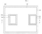
- FIG. 1 is a plan view showing a light emitting device according to an embodiment.
- FIG. 2 is a sectional view taken along line I-I' of FIG. 1 .
- a light emitting device 100 includes a substrate 105, a light emitting structure 110, the first and second electrode pads 151 and 152, and the first and second current blocking patterns 161 and 162.
- the light emitting device 100 may emit light having an UV-C wavelength, that is, an ultraviolet ray wavelength in the range of 100 nmto 280 nm.
- the light emitting device 100 is not limited to the above, and may emit light having at least one of a visible-ray wavelength and infrared-ray wavelength.
- the substrate 105 on which a GaN-based semiconductor layer may be grown, may include a transparent, insulating or conductive substrate.
- the substrate 105 may be formed by using one of Al 2 O 3 , SiC, Si, GaAs, GaN, ZnO, Si, GaP, InP, Ge, Ga 2 O 3 , LiGaO 3 , and quartz.
- a plurality of protrusions may be formed on a top surface of the substrate 105.
- the protrusions may be formed through an etching scheme or may be formed in a light extracting structure such as a separated roughness.
- the protrusion may be formed in a strip, hemispherical or dome shape.
- a buffer layer (not shown) may be further formed on the substrate 105.
- the buffer layer may attenuate the lattice mismatch between the substrate 105 and the nitride semiconductor layer and may work as a defect control layer.
- the buffer layer may have a lattice constant between a lattice constant of the substrate 11 and a lattice constant of the nitride-based semiconductor layer.
- the buffer layer may be formed of oxide such as ZnO, but the embodiment is not limited thereto.
- the light emitting structure 110 is disposeddisposed on the substrate 105.
- the light emitting structure 110 includes first and second conductive semiconductor layers 112 and 116 and an active layer 114.
- the first conductive semiconductor layer 112 may be formed in a single layer or multiple layer structure.
- the first conductive semiconductor layer 112 may be a group III-V compound semiconductor doped with a first conductive dopant.
- the first conductive dopant may include Si, Ge, Sn, Se or Te as an N-type dopant, but the embodiment is not limited thereto.
- the first conductive semiconductor layer 112 may include a semiconductor material having a compositional formula of In x Al y Ga 1-x-y N (0 ⁇ x ⁇ 1, 0 ⁇ y ⁇ 1, 0 ⁇ x+y ⁇ 1).
- the first conductive semiconductor layer 112 may include at least one of GaN, InN, AlN, InGaN, AlGaN, InAlGaN, AlInN, AlGaAs, InGaAs, AlInGaAs, GaP, AlGaP, InGaP, AlInGaP and InP.
- the active layer 114 may be formed in at least one of a single quantum well structure, a multiple quantum well (MQW) structure, a quantum wire structure and a quantum dot structure.
- the active layer 114 may include a well layer and a barrier layer formed of GeN-based semiconductor layer.
- the active layer 114 may include at least one of InGaN/GaN, InGaN/InGaN, GaN/AlGaN, InAlGaN/GaN, GaAs/AlGaAs, InGaAs/AlGaAs, GalnP/AlGaInP, GaP/AlGaP and InGaP/AlGaP, but the embodiment is not limited thereto.
- the well layer may be formed of a material having a bandgap lower than that of the barrier layer.
- the barrier layer and the well layer of the active layer 114 may be implemented as undoped layers which are not doped with impurity in order to improve the crystalline quality of the active layer 114, but impurity may be partially or entirely doped into the active area to decrease the forward voltage.
- the second conductive semiconductor layer 116 may be disposeddisposed on the active layer 114 and formed in a single layer or multiple layer structure.
- the second conductive semiconductor layer 116 may include group III-V compound semiconductor doped with a second conductive dopant.
- the second conductive dopant may include Mg, Zn, Ca, Sr or Ba as a P-type dopant, but the embodiment is not limited thereto.
- the second conductive semiconductor layer 116 may be formed of a compound semiconductor such as GaN, AlN, AlGaN, InGaN, InN, InAlGaN, AlInN, AlGaAs, GaP, GaAs, GaAsP, AlGaInP or GaP.
- the first electrode pad 151 may be disposeddisposed on the first conductive semiconductor layer 112.
- the second electrode pad 152 may be disposeddisposed on the second conductive semiconductor layer 116.
- the first and second electrode pads 151 and 152 may be formed of at least one selected from the group consisting of Ti, Ru, Rh, Ir, Mg, Zn, Al, In, Ta, Pd, Co, Ni, Si, Ge, Ag, Au and an alloy thereof.
- the first current blocking pattern 161 may be disposeddisposed on the first conductive semiconductor layer 112.
- the first current blocking pattern 161 may be disposeddisposed under the first electrode pad 151.
- the first current blocking pattern 161 may overlap an edge of the first electrode pad 151. That is, the first current blocking pattern 161 may extend along the edge of the first electrode pad 151 without disconnection.
- the first current blocking pattern 161 may be disposeddisposed between the edge of the first electrode pad 151 and the first conductive semiconductor layer 112.
- a part of the first current blocking pattern 161 may have an area OA overlapping the first electrode pad 151 and the remaining part thereof may be exposed from the first electrode pad 151 to an outside. That is, the remaining part of the first current blocking pattern 161 may protrude outward beyond the edge of the first electrode pad 151.
- the first current blocking pattern 161 may make direct contact with a top surface of the first conductive semiconductor layer 112.
- the first current blocking pattern 161 may make direct contact with a bottom surface of the first electrode pad 151.
- the overlapping area OA may be in the range of 5% to 10% of the entire area of the first electrode pad 151.
- the width of the sectional surface of the overlapping area OA may be in the range o 5 ⁇ m to 15 ⁇ m.
- the overlapping area OA may be less than 5% of the entire area of the first electrode pad 151 or the width of the sectional surface of the overlapping area OA may be less than 5 ⁇ m, it may be difficult to obtain a current blocking effect due to the misalignment between the first electrode pad 151 and the first current blocking pattern 161.
- the overlapping area OA may exceed 15% of the entire area of the first electrode pad 151 or the width of the sectional surface thereof may exceed 5 ⁇ m, the current blocking area may be enlarged so that the light efficiency may be deteriorated.
- the first current blocking pattern 161 performs a function of blocking current concentrated on the edge of the first electrode pad 151.
- the first current blocking pattern 161 may prevent current from being crowded into the edge of the first electrode pad 151.
- the light emitting device 100 may include an ultraviolet ray light emitting device having a driving voltage higher than that of a conventional visible ray light emitting device, and thus, a current crowding phenomenon may occur in the area adjacent to the first electrode pad 151.
- the first current blocking pattern 161 may block the current concentrated on the edge of the first electrode pad 151.
- the light emitting device 100 may prevent the edge of the first electrode pad 151 from being damaged due to the current crowding phenomenon so that the stability of the light emitting device 100 may be improved.
- the second current blocking pattern 162 may be disposed on the second conductive semiconductor layer 116.
- the second current blocking pattern 162 may be disposeddisposed under the second electrode pad 151.
- the second current blocking pattern 162 may overlap an edge of the second electrode pad 152. That is, the second current blocking pattern 162 may extend along the edge of the second electrode pad 152 without disconnection.
- the second current blocking pattern 162 may be disposeddisposed between the edge of the second electrode pad 152 and the second conductive semiconductor layer 116.
- a part of the second current blocking pattern 162 may have an area OA overlapping the second electrode pad 152 and the remaining part thereof may be exposed from the second electrode pad 152 to an outside. That is, the remaining part of the second current blocking pattern 162 may protrude outward beyond the edge of the second electrode pad 152.
- the second current blocking pattern 162 may make direct contact with a top surface of the second conductive semiconductor layer 116.
- the second current blocking pattern 162 may make direct contact with a bottom surface of the second electrode pad 152.
- the overlapping area OA may be in the range of 5% to 10% of the entire area of the second electrode pad 152.
- the width of the sectional surface of the overlapping area OA may be in the range o 5 ⁇ m to 15 ⁇ m.
- the overlapping area OA may be less than 5% of the entire area of the second electrode pad 152 or the width of the sectional surface of the overlapping area OA may be less than 5 ⁇ m, it may be difficult to obtain the current blocking effect due to the misalignment between the second electrode pad 152 and the second current blocking pattern 162.
- the overlapping area OA may exceed 15% of the entire area of the second electrode pad 152 or the width of the sectional surface thereof may exceed 5 ⁇ m, the current blocking area may be enlarged so that the light efficiency may be deteriorated.
- the second current blocking pattern 162 performs the function of blocking current concentrated on the edge of the second electrode pad 152. That is, the second current blocking pattern 161 may prevent current from being crowded into the edge of the second electrode pad 152.
- the light emitting device 100 may include an ultraviolet ray light emitting device having a driving voltage higher than that of a conventional visible ray light emitting device, and thus, a current crowding phenomenon may occur in the area adjacent to the second electrode pad 152.
- the second current blocking pattern 162 may block the current concentrated on the edge of the second electrode pad 152.
- the light emitting device 100 may prevent the edge of the second electrode pad 152 from being damaged due to the current crowding phenomenon so that the stability of the light emitting device 100 may be improved.
- the first and second current blocking patterns 161 and 162 may be simultaneously formed and each may have a thickness in the range go 100 nm to 300 nm.
- the embodiment is not limited thereto and thus, the light emitting device 100 may include only the first or second current blocking pattern 161 or 162.
- the embodiment is not limited thereto and the edges of the first and second current blocking patterns 161 and 162 may be disposed in parallel with the edges of the first and second electrode pads 151 and 152, respectively. That is, the whole of the first current blocking pattern 161 may overlap the first electrode pad 151 and the whole of the second current blocking pattern 162 may overlap the second electrode pad 152.
- the light emitting device 100 may be prevented from being damaged due to the current crowding near the edges of the first and second electrode pads 151 and 152, so that the stability of the ultraviolet ray light emitting device emitting light having an ultraviolet ray wavelength may be improved.
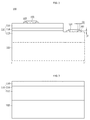
- FIGS. 3 to 6 are views illustrating a method of manufacturing a light emitting device according to the embodiment.
- the light emitting device includes a semiconductor structure 110 on a substrate 100.
- the substrate 105 may be formed of a material having superior thermal conductivity and may be a conductive substrate or an insulating substrate.
- the substrate 105 may include at least one of GaAs, Al 2 O 3 , SiC, Si, GaN, ZnO, GaP, InP, Ge and Ga 2 O 3 .
- a concave-convex structure P may be formed on the substrate 105, but the embodiment is not limited thereto. Impurities may be removed from the surface of the substrate 105 through wet cleaning.
- a buffer layer (not shown) may be formed on the substrate 105.
- the buffer layer may relieve the lattice mismatch between a material of the light emitting structure 110 and the substrate 105.
- the buffer layer may be formed of group III-V compound semiconductor, for example at least one of GaN, InN, AlN, InGaN, AlGaN, InAlGaN and AlInN.
- An undoped semiconductor layer (not shown) may be formed on the buffer layer, but the embodiment is not limited thereto.
- the light emitting structure 110 including the first and second conductive semiconductor layers 112 and 116 and the active layer 114 may be formed on the substrate 105 or the buffer layer.
- the first conductive semiconductor layer 112 may be formed of a semiconductor compound, such as group III-V or group II-VI compound semiconductor, and doped with the first conductive dopant.
- the first conductive dopant may be an N-type dopant, such as Si, Ge, Sn, Se or Te, but the embodiment is not limited thereto.
- the first conductive semiconductor layer 112 may include a semiconductor material having a compositional formula of In x Al y Ga 1-x-y P (0 ⁇ x ⁇ 1, 0 ⁇ y ⁇ 1, 0 ⁇ x+y ⁇ 1) or In x Al y Ga 1-x-y N (0 ⁇ x ⁇ 1, 0 ⁇ y ⁇ 1, 0 ⁇ x+y ⁇ 1).
- the first conductive semiconductor layer 112 may be formed of at least one of AlGaP, InGaP, AlInGaP, InP, GaN, InN, AlN, InGaN, AlGaN, InAlGaN, AlInN, AlGaAs, InGaAs, AlInGaAs and GaP.
- the first conductive semiconductor layer 112 may be formed through a chemical deposition vapor (CDV) scheme, a molecular beam epitaxy (MBE) scheme, a sputtering scheme, or a hydride vapor phase epitaxy (HVPE) scheme, but the embodiment is not limited thereto.
- CDV chemical deposition vapor
- MBE molecular beam epitaxy
- HVPE hydride vapor phase epitaxy
- Electrons injected through the first conductive semiconductor layer 112 are combined with holes injected through the second conductive semiconductor layer 116 at the active layer 114, so the active layer 114 emits light having the energy which is determined according to a typical energy band of a material constituting the active layer 114 (light emitting layer).
- the active layer 114 may include at least one of a single quantum well structure, a multi quantum well (MQW) structure, a quantum wire structure and a quantum dot structure.
- MQW multi quantum well
- the active layer 114 may include a structure of well layer/barrier layer.
- the active layer 114 may include at least one of GalnP/AlGaInP, GaP/AlGaP, InGaP/AlGaP, InGaN/GaN, InGaN/InGaN, GaN/AlGaN, InAlGaN/GaN, GaAs/AlGaAs and InGaAs/AlGaAs, but the embodiment is not limited thereto.
- the well layer may be formed of a material having a bandgap lower than that of the barrier layer.
- the second conductive semiconductor layer 116 may be formed of a semiconductor compound, such as group III-V or group II-VI compound semiconductor, and doped with the second conductive dopant.
- the second conductive semiconductor layer 116 may include a semiconductor material having a compositional formula of In x Al y Ga 1-x-y P (0 ⁇ x ⁇ 1, 0 ⁇ y ⁇ 1, 0 ⁇ x+y ⁇ 1) or In x Al y Ga 1-x-y N (0 ⁇ x ⁇ 1, 0 ⁇ y ⁇ 1, 0 ⁇ x+y ⁇ 1).
- the second conductive dopant may be a P-type dopant such as Mg, Zn, Ca, Sr or Ba.
- the first conductive semiconductor layer 112 may be illustrated as an N-type semiconductor layer and the second conductive semiconductor layer 116 may be illustrated as a P-type semiconductor layer in the embodiment, the embodiment is not limited thereto.
- a semiconductor layer having polarity opposite to that of the second conductive semiconductor layer 116 for instance, an N-type semiconductor layer (not shown) may be formed on the second conductive semiconductor layer 116.
- the light emitting structure 110 may have one of an N-P junction structure, a P-N junction structure, an N-P-N junction structure and a P-N-P junction structure.
- the active layer 114 and the first and second conductive semiconductor layers 112 and 116 may be partially removed to expose the first conductive semiconductor layer 112.
- the process may be performed through a wet etching scheme or a dry etching scheme, but the embodiment is not limited thereto.
- the first current blocking pattern 161 may be formed on the exposed first conductive semiconductor layer 112 and the second current blocking pattern 162 may be formed on the second conductive semiconductor layer 116.
- the first and second current blocking patterns 161 and 162 may be formed through an etching process using photoresist, but the embodiment is not limited thereto.
- the first and second current blocking patterns 161 and 162 may be implemented by using oxide or nitride.
- the current blocking layer 160 may be formed of at least one selected from the group consisting of SiO 2 , SiNX, Si x O y , Si x N y , SiO x N y , Al 2 O 3 , TiO 2 and AlN, but the embodiment is not limited thereto.
- the first and second current blocking patterns 161 and 162 may be formed in a ring type without disconnection.
- the first electrode pad 151 may be disposeddisposed on the exposed first conductive semiconductor layer 112 and the second electrode pad 152 may be formed on the second conductive semiconductor layer 116.
- the first electrode pad 151 may be formed in the compartment formed by the first current blocking pattern 161.
- the edge of the first electrode pad 151 may have the area OA overlapping the first current blocking pattern 161 and may be disposeddisposed in parallel with the edge of the first current blocking pattern 161.
- the second electrode pad 152 may be formed in the compartment formed by the second current blocking pattern 162.
- the edge of the second electrode pad 152 may have the area OA overlapping the second current blocking pattern 162 and may be disposeddisposed in parallel with the edge of the second current blocking pattern 162.
- the first and second electrode pads 151 and 152 may be formed at least one of Ti, Cr, Ni, Al, Pt, Au, W and Mo, but the embodiment is not limited thereto.
- the light emitting device 100 may be prevented from being damaged due to the current crowding near the edges of the first and second electrode pads 151 and 152, so that the stability of the ultraviolet ray light emitting device emitting light having an ultraviolet ray wavelength may be improved.
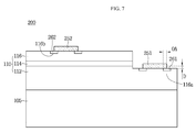
- FIG. 7 is a sectional view showing a light emitting device according to another embodiment.
- Another embodiment may employ the technical properties of the embodiment of FIGS. 1 to 6 .
- the configuration of the light emitting device 200 according to another embodiment is the same as that of the light emitting device 100 according to the embodiment of FIG. 1 except for the first and second current blocking patterns 261 and 262 and the first and second electrode pads 251 and 252, the same references will be assigned to the same elements and the details thereof will be omitted. In the following description, the main features of another embodiment will be focused.
- the light emitting structure 110 is disposed on the substrate 105.
- the light emitting structure 110 includes the first and second conductive semiconductor layers 112 and 116 and the active layer 114.
- the first conductive semiconductor layer 112 includes a first containing groove 112a.
- the first containing groove 112a may be formed in a ring type without disconnection.
- the second conductive semiconductor layer 116 includes a second containing groove 116a.
- the second containing groove 116a may be formed in a ring type without disconnection.
- the first current blocking pattern 261 may be formed in the first containing groove 112a. Top surfaces of the first current blocking pattern 261 and the first conductive semiconductor layer 112 may be disposed on the same plane.
- the second current blocking pattern 262 may be formed in the second containing groove 116a. Top surfaces of the second current blocking pattern 262 and the second conductive semiconductor layer 116 may be disposed on the same plane.
- the first and second current blocking patterns 261 and 262 may be simultaneously formed and each may have a thickness D in the range go 100 nm to 300 nm.
- the first and second current blocking patterns 261 and 262 may be implemented by using oxide or nitride.
- the first and second current blocking layers 261 and 262 may be formed of at least one selected from the group consisting of SiO 2 , SiNX, Si x O y , Si x N y , SiO x N y , Al 2 O 3 , TiO 2 and AlN, but the embodiment is not limited thereto.
- the first and second current blocking patterns are formed on the first and second conductive semiconductor layers, respectively, so that the light emitting device may be prevented from being damaged due to the current crowding near the edges of the first and second electrode pads.
- the stability of the ultraviolet light emitting device which emits light having an ultraviolet ray wavelength and has a high driving voltage, may be improved.
- FIG. 8 is a sectional view showing a light emitting device according to still another embodiment.
- Still another embodiment may employ the technical properties of the embodiment of FIGS. 1 to 6 .
- the configuration of the light emitting device 300 according to still another embodiment is the same as that of the light emitting device 100 according to the embodiment of FIG. 1 except for the first and second current blocking patterns 361 and 362 and the first and second electrode pads 351 and 352, the same references will be assigned to the same elements and the details thereof will be omitted. In the following description, the main features of still another embodiment will be focused.
- the light emitting structure 110 is disposed on the substrate 105.
- the light emitting structure 110 includes the first and second conductive semiconductor layers 112 and 116 and the active layer 114.
- the first current blocking pattern 361 may be formed in the first conductive semiconductor layer 112.
- the first current blocking pattern 361 may include a dopant different from a dopant of the first conductive semiconductor layer 112.
- the first current blocking pattern 361 may include Mg, Zn, Ca, Sr or Ba as a P-type dopant, but the embodiment is not limited thereto.
- Top surfaces of the first current blocking pattern 361 and the first conductive semiconductor layer 112 may be disposeddisposed on the same plane.
- the second current blocking pattern 362 may be formed in the second conductive semiconductor layer 112.
- the second current blocking pattern 362 may include a dopant different from a dopant of the second conductive semiconductor layer 116.
- the second current blocking pattern 362 may include Si, Ge, Sn, Se or Te as a N-type dopant, but the embodiment is not limited thereto.
- Top surfaces of the second current blocking pattern 362 and the second conductive semiconductor layer 116 may be disposeddisposed on the same plane.
- the first and second current blocking patterns 361 and 362 may be simultaneously formed and each may have a thickness in the range go 100 nm to 300 nm.
- the first current blocking pattern 361 may be formed in the first conductive semiconductor layer 112 and the second current blocking pattern 362 may be formed in the second conductive semiconductor layer 116 through an ion implantation scheme, so that the light emitting device 300 may be prevented from being damaged due to the current crowding near the edges of the first and second electrode pads 351 and 352.
- the stability of the ultraviolet light emitting device which emits light having an ultraviolet ray wavelength and has a high driving voltage, may be improved.
- FIG. 9 is a sectional view showing a light emitting device package including a light emitting device according to an embodiment.
- the light emitting device package 700 includes a body 750, first and second lead electrodes 721 and 723, at least part of which is disposed on the body 750, a light emitting device 800 provided on the body 750 and electrically connected to the first and second lead electrodes 721 and 723, and a molding member 730 that surrounds the light emitting device 100 on the body 750.
- the light emitting device 800 may employ the technical features of FIGS. 1 to 8 .
- the body 750 may include silicon, synthetic resin or metallic material.
- the first and second lead electrodes 131 and 132 may be electrically isolated from each other and pass through the inside of the body 750. That is, parts of the first and second lead electrodes 721 and 723 may be disposed in a cavity and other parts may be disposed to an outside of the body 750.
- Electric power may be supplied to the light emitting device 800 through the first and second lead electrodes 721 and 723 and the light generated from the light emitting device 800 may be reflected upon the first and second lead electrodes 721 and 723, so that the light efficiency may be improved and the heat generated from the light emitting device 800 may be discharged.
- the light emitting device package 700 may be applied to the light unit.
- the light unit may include a structure in which a plurality of light emitting devices or light emitting packages is arrayed and may include a lamp, a signal lamp, a headlight of a vehicle and an electric sign board.
- any reference in this specification to "one embodiment,” “an embodiment,” “example embodiment,” etc. means that a particular feature, structure, or characteristic described in connection with the embodiment is included in at least one embodiment of the invention.
- the appearances of such phrases in various places in the specification are not necessarily all referring to the same embodiment.
Landscapes
- Led Devices (AREA)
Abstract
Description
- The present application claims priority under 35 U.S.C. 119 to Korean Patent Application No.
10-2015-0014198 filed on January 29, 2015 - The embodiment relates to a light emitting device and a light emitting device package.
- A light emitting device (LED) includes a p-n junction diode having a characteristic of converting electric energy into light energy. The p-n junction diode can be formed by combining group III-V elements of the periodic table. The light emitting device can represent various colors by adjusting the compositional ratio of compound semiconductors.
- A GaN-based light emitting device (LED) has been used in various applications such as a natural color LED display, an LED traffic signal device or a white color LED. In recent years, the luminous efficiency of a high-efficiency white color LED is superior to that of a conventional fluorescent lamp, so that it is expected in a general lighting field that the white color LED will replace the fluorescent lamp.
- According to a light emitting device of the related art, an electrode may be damaged due to a current crowding phenomenon that concentrates current on the edges of electrodes by a high voltage such as static electricity. In particular, according to a light emitting device of the related art, the edges of the electrodes of an ultraviolet light emitting device using a high driving voltage may be damaged due to the current crowding phenomenon.
- The embodiment is to provide a light emitting device and a light emitting device package capable of improving reliability.
- The embodiment is to provide a stable light emitting device and a stable light emitting device package.
- According to an embodiment, there is provided a light emitting device which includes a light emitting structure including a first conductive semiconductor layer, an active layer on the first conductive semiconductor layer and a second conductive semiconductor layer on the active layer; a first electrode pad on the first conductive semiconductor layer; a second electrode pad on the second conductive semiconductor layer; and a current blocking pattern overlapping an edge of at least one of the first and second electrode pads.
- A light emitting device package according to an embodiment may include the light emitting device.
- According to one embodiment, the light emitting device may be prevented from being damaged due to the current crowding near the edges of the first and second electrode pads, so that the stability of the ultraviolet light emitting device, which emits light having an ultraviolet ray wavelength and has a high driving voltage, may be improved.
- According to another embodiment, the first and second current blocking patterns are formed on the first and second conductive semiconductor layers, respectively, so that the light emitting device may be prevented from being damaged due to the current crowding near the edges of the first and second electrode pads. Thus, the stability of the ultraviolet light emitting device, which emits light having an ultraviolet ray wavelength and has a high driving voltage, may be improved.
- According to the light emitting device of still another embodiment, the first current blocking pattern may be formed in the first conductive semiconductor layer and the second current blocking pattern may be formed in the second conductive semiconductor layer through an ion implantation scheme, so that the light emitting device may be prevented from being damaged due to the current crowding near the edges of the first and second electrode pads. Thus, the stability of the ultraviolet light emitting device, which emits light having an ultraviolet ray wavelength and has a high driving voltage, may be improved.
-
-
FIG. 1 is a plan view showing a light emitting device according to one embodiment. -
FIG. 2 is a sectional view taken along line I-I' ofFIG. 1 . -
FIGS. 3 to 6 are views illustrating a method of manufacturing a light emitting device according to the embodiment. -
FIG. 7 is a sectional view showing a light emitting device according to another embodiment. -
FIG. 8 is a sectional view showing a light emitting device according to still another embodiment -
FIG. 9 is a sectional view showing a light emitting device package including a light emitting device according to an embodiment. - Hereinafter, a light emitting device and a light emitting device package according to the embodiment will be described with reference to accompanying drawings. In the description of the embodiments, it will be understood that, when a layer (or film), an area, a pattern, or a structure is referred to as being "on" or "under" another substrate, another layer (or film), another area, another pad, or another pattern, it can be "directly" or "indirectly" over the other substrate, layer (or film), area, pad, or pattern, or one or more intervening layers may also be present. Such a position of the layer has been described with reference to the drawings.
-
FIG. 1 is a plan view showing a light emitting device according to an embodiment.FIG. 2 is a sectional view taken along line I-I' ofFIG. 1 . - Referring to
FIGS. 1 and2 , alight emitting device 100 according to an embodiment includes asubstrate 105, alight emitting structure 110, the first andsecond electrode pads current blocking patterns - The
light emitting device 100 may emit light having an UV-C wavelength, that is, an ultraviolet ray wavelength in the range of 100 nmto 280 nm. Thelight emitting device 100 is not limited to the above, and may emit light having at least one of a visible-ray wavelength and infrared-ray wavelength. - The
substrate 105, on which a GaN-based semiconductor layer may be grown, may include a transparent, insulating or conductive substrate. For example, thesubstrate 105 may be formed by using one of Al2O3, SiC, Si, GaAs, GaN, ZnO, Si, GaP, InP, Ge, Ga2O3, LiGaO3, and quartz. A plurality of protrusions may be formed on a top surface of thesubstrate 105. The protrusions may be formed through an etching scheme or may be formed in a light extracting structure such as a separated roughness. The protrusion may be formed in a strip, hemispherical or dome shape. - . Although not shown in the drawings, a buffer layer (not shown) may be further formed on the
substrate 105. The buffer layer may attenuate the lattice mismatch between thesubstrate 105 and the nitride semiconductor layer and may work as a defect control layer. - The buffer layer may have a lattice constant between a lattice constant of the substrate 11 and a lattice constant of the nitride-based semiconductor layer. The buffer layer may be formed of oxide such as ZnO, but the embodiment is not limited thereto.
- The
light emitting structure 110 is disposeddisposed on thesubstrate 105. Thelight emitting structure 110 includes first and secondconductive semiconductor layers active layer 114. - The first
conductive semiconductor layer 112 may be formed in a single layer or multiple layer structure. When the firstconductive semiconductor layer 112 is an N-type semiconductor layer, the firstconductive semiconductor layer 112 may be a group III-V compound semiconductor doped with a first conductive dopant. The first conductive dopant may include Si, Ge, Sn, Se or Te as an N-type dopant, but the embodiment is not limited thereto. The firstconductive semiconductor layer 112 may include a semiconductor material having a compositional formula of InxAlyGa1-x-yN (0≤x≤1, 0 ≤y≤1, 0≤x+y≤1). The firstconductive semiconductor layer 112 may include at least one of GaN, InN, AlN, InGaN, AlGaN, InAlGaN, AlInN, AlGaAs, InGaAs, AlInGaAs, GaP, AlGaP, InGaP, AlInGaP and InP. - The
active layer 114 may be formed in at least one of a single quantum well structure, a multiple quantum well (MQW) structure, a quantum wire structure and a quantum dot structure. Theactive layer 114 may include a well layer and a barrier layer formed of GeN-based semiconductor layer. - For example, the
active layer 114 may include at least one of InGaN/GaN, InGaN/InGaN, GaN/AlGaN, InAlGaN/GaN, GaAs/AlGaAs, InGaAs/AlGaAs, GalnP/AlGaInP, GaP/AlGaP and InGaP/AlGaP, but the embodiment is not limited thereto. The well layer may be formed of a material having a bandgap lower than that of the barrier layer. - The barrier layer and the well layer of the
active layer 114 may be implemented as undoped layers which are not doped with impurity in order to improve the crystalline quality of theactive layer 114, but impurity may be partially or entirely doped into the active area to decrease the forward voltage. - The second
conductive semiconductor layer 116 may be disposeddisposed on theactive layer 114 and formed in a single layer or multiple layer structure. When the secondconductive semiconductor layer 116 is a P-type semiconductor layer, the secondconductive semiconductor layer 116 may include group III-V compound semiconductor doped with a second conductive dopant. The second conductive dopant may include Mg, Zn, Ca, Sr or Ba as a P-type dopant, but the embodiment is not limited thereto. For example, the secondconductive semiconductor layer 116 may be formed of a compound semiconductor such as GaN, AlN, AlGaN, InGaN, InN, InAlGaN, AlInN, AlGaAs, GaP, GaAs, GaAsP, AlGaInP or GaP. - The
first electrode pad 151 may be disposeddisposed on the firstconductive semiconductor layer 112. - The
second electrode pad 152 may be disposeddisposed on the secondconductive semiconductor layer 116. - The first and
second electrode pads - The first
current blocking pattern 161 may be disposeddisposed on the firstconductive semiconductor layer 112. The firstcurrent blocking pattern 161 may be disposeddisposed under thefirst electrode pad 151. The firstcurrent blocking pattern 161 may overlap an edge of thefirst electrode pad 151. That is, the firstcurrent blocking pattern 161 may extend along the edge of thefirst electrode pad 151 without disconnection. The firstcurrent blocking pattern 161 may be disposeddisposed between the edge of thefirst electrode pad 151 and the firstconductive semiconductor layer 112. A part of the firstcurrent blocking pattern 161 may have an area OA overlapping thefirst electrode pad 151 and the remaining part thereof may be exposed from thefirst electrode pad 151 to an outside. That is, the remaining part of the firstcurrent blocking pattern 161 may protrude outward beyond the edge of thefirst electrode pad 151. The firstcurrent blocking pattern 161 may make direct contact with a top surface of the firstconductive semiconductor layer 112. The firstcurrent blocking pattern 161 may make direct contact with a bottom surface of thefirst electrode pad 151. For example, the overlapping area OA may be in the range of 5% to 10% of the entire area of thefirst electrode pad 151. The width of the sectional surface of the overlapping area OA may be in the range o 5 µm to 15 µm. When the overlapping area OA may be less than 5% of the entire area of thefirst electrode pad 151 or the width of the sectional surface of the overlapping area OA may be less than 5 µm, it may be difficult to obtain a current blocking effect due to the misalignment between thefirst electrode pad 151 and the firstcurrent blocking pattern 161. In addition, when the overlapping area OA may exceed 15% of the entire area of thefirst electrode pad 151 or the width of the sectional surface thereof may exceed 5 µm, the current blocking area may be enlarged so that the light efficiency may be deteriorated. The firstcurrent blocking pattern 161 performs a function of blocking current concentrated on the edge of thefirst electrode pad 151. That is, the firstcurrent blocking pattern 161 may prevent current from being crowded into the edge of thefirst electrode pad 151. For example, thelight emitting device 100 may include an ultraviolet ray light emitting device having a driving voltage higher than that of a conventional visible ray light emitting device, and thus, a current crowding phenomenon may occur in the area adjacent to thefirst electrode pad 151. - The first
current blocking pattern 161 according to the embodiment may block the current concentrated on the edge of thefirst electrode pad 151. Thus, thelight emitting device 100 according to the embodiment may prevent the edge of thefirst electrode pad 151 from being damaged due to the current crowding phenomenon so that the stability of thelight emitting device 100 may be improved. - The second
current blocking pattern 162 may be disposed on the secondconductive semiconductor layer 116. The secondcurrent blocking pattern 162 may be disposeddisposed under thesecond electrode pad 151. The secondcurrent blocking pattern 162 may overlap an edge of thesecond electrode pad 152. That is, the secondcurrent blocking pattern 162 may extend along the edge of thesecond electrode pad 152 without disconnection. The secondcurrent blocking pattern 162 may be disposeddisposed between the edge of thesecond electrode pad 152 and the secondconductive semiconductor layer 116. A part of the secondcurrent blocking pattern 162 may have an area OA overlapping thesecond electrode pad 152 and the remaining part thereof may be exposed from thesecond electrode pad 152 to an outside. That is, the remaining part of the secondcurrent blocking pattern 162 may protrude outward beyond the edge of thesecond electrode pad 152. The secondcurrent blocking pattern 162 may make direct contact with a top surface of the secondconductive semiconductor layer 116. The secondcurrent blocking pattern 162 may make direct contact with a bottom surface of thesecond electrode pad 152. For example, the overlapping area OA may be in the range of 5% to 10% of the entire area of thesecond electrode pad 152. The width of the sectional surface of the overlapping area OA may be in the range o 5 µm to 15 µm. When the overlapping area OA may be less than 5% of the entire area of thesecond electrode pad 152 or the width of the sectional surface of the overlapping area OA may be less than 5 µm, it may be difficult to obtain the current blocking effect due to the misalignment between thesecond electrode pad 152 and the secondcurrent blocking pattern 162. In addition, when the overlapping area OA may exceed 15% of the entire area of thesecond electrode pad 152 or the width of the sectional surface thereof may exceed 5 µm, the current blocking area may be enlarged so that the light efficiency may be deteriorated. - The second
current blocking pattern 162 performs the function of blocking current concentrated on the edge of thesecond electrode pad 152. That is, the secondcurrent blocking pattern 161 may prevent current from being crowded into the edge of thesecond electrode pad 152. For example, thelight emitting device 100 may include an ultraviolet ray light emitting device having a driving voltage higher than that of a conventional visible ray light emitting device, and thus, a current crowding phenomenon may occur in the area adjacent to thesecond electrode pad 152. - The second
current blocking pattern 162 according to the embodiment may block the current concentrated on the edge of thesecond electrode pad 152. Thus, thelight emitting device 100 according to the embodiment may prevent the edge of thesecond electrode pad 152 from being damaged due to the current crowding phenomenon so that the stability of thelight emitting device 100 may be improved. - The first and second current blocking
patterns - Although the
light emitting device 100 including all the first and second current blockingpatterns light emitting device 100 may include only the first or secondcurrent blocking pattern - According to the
light emitting device 100 of the embodiment, although the part of the firstcurrent blocking pattern 161 protruding outward beyond the edge of thefirst electrode pad 151 and the part of the secondcurrent blocking pattern 162 protruding outward beyond the edge of thesecond electrode pad 152 have been described, the embodiment is not limited thereto and the edges of the first and second current blockingpatterns second electrode pads current blocking pattern 161 may overlap thefirst electrode pad 151 and the whole of the secondcurrent blocking pattern 162 may overlap thesecond electrode pad 152. - The
light emitting device 100 according to the embodiment may be prevented from being damaged due to the current crowding near the edges of the first andsecond electrode pads -
FIGS. 3 to 6 are views illustrating a method of manufacturing a light emitting device according to the embodiment. - Referring to
FIG. 3 , the light emitting device according to an embodiment includes asemiconductor structure 110 on asubstrate 100. - The
substrate 105 may be formed of a material having superior thermal conductivity and may be a conductive substrate or an insulating substrate. For example, thesubstrate 105 may include at least one of GaAs, Al2O3, SiC, Si, GaN, ZnO, GaP, InP, Ge and Ga2O3. A concave-convex structure P may be formed on thesubstrate 105, but the embodiment is not limited thereto. Impurities may be removed from the surface of thesubstrate 105 through wet cleaning. - A buffer layer (not shown) may be formed on the
substrate 105. The buffer layer may relieve the lattice mismatch between a material of thelight emitting structure 110 and thesubstrate 105. The buffer layer may be formed of group III-V compound semiconductor, for example at least one of GaN, InN, AlN, InGaN, AlGaN, InAlGaN and AlInN. An undoped semiconductor layer (not shown) may be formed on the buffer layer, but the embodiment is not limited thereto. - The
light emitting structure 110 including the first and second conductive semiconductor layers 112 and 116 and theactive layer 114 may be formed on thesubstrate 105 or the buffer layer. - The first
conductive semiconductor layer 112 may be formed of a semiconductor compound, such as group III-V or group II-VI compound semiconductor, and doped with the first conductive dopant. When the firstconductive semiconductor layer 112 is an N-type semiconductor layer, the first conductive dopant may be an N-type dopant, such as Si, Ge, Sn, Se or Te, but the embodiment is not limited thereto. - The first
conductive semiconductor layer 112 may include a semiconductor material having a compositional formula of InxAlyGa1-x-yP (0≤x≤1, 0≤y≤1, 0≤x+y≤1) or InxAlyGa1-x-yN (0≤x≤1, 0≤y≤1, 0≤x+y≤1). - The first
conductive semiconductor layer 112 may be formed of at least one of AlGaP, InGaP, AlInGaP, InP, GaN, InN, AlN, InGaN, AlGaN, InAlGaN, AlInN, AlGaAs, InGaAs, AlInGaAs and GaP. - The first
conductive semiconductor layer 112 may be formed through a chemical deposition vapor (CDV) scheme, a molecular beam epitaxy (MBE) scheme, a sputtering scheme, or a hydride vapor phase epitaxy (HVPE) scheme, but the embodiment is not limited thereto. - Electrons injected through the first
conductive semiconductor layer 112 are combined with holes injected through the secondconductive semiconductor layer 116 at theactive layer 114, so theactive layer 114 emits light having the energy which is determined according to a typical energy band of a material constituting the active layer 114 (light emitting layer). - The
active layer 114 may include at least one of a single quantum well structure, a multi quantum well (MQW) structure, a quantum wire structure and a quantum dot structure. - The
active layer 114 may include a structure of well layer/barrier layer. Theactive layer 114 may include at least one of GalnP/AlGaInP, GaP/AlGaP, InGaP/AlGaP, InGaN/GaN, InGaN/InGaN, GaN/AlGaN, InAlGaN/GaN, GaAs/AlGaAs and InGaAs/AlGaAs, but the embodiment is not limited thereto. The well layer may be formed of a material having a bandgap lower than that of the barrier layer. - The second
conductive semiconductor layer 116 may be formed of a semiconductor compound, such as group III-V or group II-VI compound semiconductor, and doped with the second conductive dopant. For example, the secondconductive semiconductor layer 116 may include a semiconductor material having a compositional formula of InxAlyGa1-x-yP (0≤x≤1, 0≤y≤1, 0≤x+y≤1) or InxAlyGa1-x-yN (0≤x≤1, 0≤y≤1, 0≤x+y≤1). When the secondconductive semiconductor layer 116 is a P-type semiconductor layer, the second conductive dopant may be a P-type dopant such as Mg, Zn, Ca, Sr or Ba. - Although the first
conductive semiconductor layer 112 may be illustrated as an N-type semiconductor layer and the secondconductive semiconductor layer 116 may be illustrated as a P-type semiconductor layer in the embodiment, the embodiment is not limited thereto. In addition, in thelight emitting structure 110, a semiconductor layer having polarity opposite to that of the secondconductive semiconductor layer 116, for instance, an N-type semiconductor layer (not shown) may be formed on the secondconductive semiconductor layer 116. Thus, thelight emitting structure 110 may have one of an N-P junction structure, a P-N junction structure, an N-P-N junction structure and a P-N-P junction structure. - Referring to
FIG. 4 , theactive layer 114 and the first and second conductive semiconductor layers 112 and 116 may be partially removed to expose the firstconductive semiconductor layer 112. In this case, the process may be performed through a wet etching scheme or a dry etching scheme, but the embodiment is not limited thereto. - Referring to
FIG. 5 , the firstcurrent blocking pattern 161 may be formed on the exposed firstconductive semiconductor layer 112 and the secondcurrent blocking pattern 162 may be formed on the secondconductive semiconductor layer 116. - The first and second current blocking
patterns - The first and second current blocking
patterns - The first and second current blocking
patterns - Referring to
FIG. 6 , thefirst electrode pad 151 may be disposeddisposed on the exposed firstconductive semiconductor layer 112 and thesecond electrode pad 152 may be formed on the secondconductive semiconductor layer 116. - The
first electrode pad 151 may be formed in the compartment formed by the firstcurrent blocking pattern 161. The edge of thefirst electrode pad 151 may have the area OA overlapping the firstcurrent blocking pattern 161 and may be disposeddisposed in parallel with the edge of the firstcurrent blocking pattern 161. - The
second electrode pad 152 may be formed in the compartment formed by the secondcurrent blocking pattern 162. The edge of thesecond electrode pad 152 may have the area OA overlapping the secondcurrent blocking pattern 162 and may be disposeddisposed in parallel with the edge of the secondcurrent blocking pattern 162. - The first and
second electrode pads - The
light emitting device 100 according to the embodiment may be prevented from being damaged due to the current crowding near the edges of the first andsecond electrode pads -
FIG. 7 is a sectional view showing a light emitting device according to another embodiment. - Another embodiment may employ the technical properties of the embodiment of
FIGS. 1 to 6 . - Referring to
FIG. 7 , since the configuration of thelight emitting device 200 according to another embodiment is the same as that of thelight emitting device 100 according to the embodiment ofFIG. 1 except for the first and second current blockingpatterns second electrode pads - The
light emitting structure 110 is disposed on thesubstrate 105. Thelight emitting structure 110 includes the first and second conductive semiconductor layers 112 and 116 and theactive layer 114. - The first
conductive semiconductor layer 112 includes a first containing groove 112a. The first containing groove 112a may be formed in a ring type without disconnection. - The second
conductive semiconductor layer 116 includes a second containinggroove 116a. The second containinggroove 116a may be formed in a ring type without disconnection. - The first
current blocking pattern 261 may be formed in the first containing groove 112a. Top surfaces of the firstcurrent blocking pattern 261 and the firstconductive semiconductor layer 112 may be disposed on the same plane. - The second
current blocking pattern 262 may be formed in the second containinggroove 116a. Top surfaces of the secondcurrent blocking pattern 262 and the secondconductive semiconductor layer 116 may be disposed on the same plane. - The first and second current blocking
patterns patterns - According to another embodiment, the first and second current blocking patterns are formed on the first and second conductive semiconductor layers, respectively, so that the light emitting device may be prevented from being damaged due to the current crowding near the edges of the first and second electrode pads. Thus, according to the
light emitting device 200 of another embodiment, the stability of the ultraviolet light emitting device, which emits light having an ultraviolet ray wavelength and has a high driving voltage, may be improved. -
FIG. 8 is a sectional view showing a light emitting device according to still another embodiment. - Still another embodiment may employ the technical properties of the embodiment of
FIGS. 1 to 6 . - Referring to
FIG. 8 , since the configuration of thelight emitting device 300 according to still another embodiment is the same as that of thelight emitting device 100 according to the embodiment ofFIG. 1 except for the first and second current blockingpatterns second electrode pads - The
light emitting structure 110 is disposed on thesubstrate 105. Thelight emitting structure 110 includes the first and second conductive semiconductor layers 112 and 116 and theactive layer 114. - The first
current blocking pattern 361 may be formed in the firstconductive semiconductor layer 112. The firstcurrent blocking pattern 361 may include a dopant different from a dopant of the firstconductive semiconductor layer 112. For example, when the firstconductive semiconductor layer 112 is an N-type semiconductor, the firstcurrent blocking pattern 361 may include Mg, Zn, Ca, Sr or Ba as a P-type dopant, but the embodiment is not limited thereto. Top surfaces of the firstcurrent blocking pattern 361 and the firstconductive semiconductor layer 112 may be disposeddisposed on the same plane. - The second
current blocking pattern 362 may be formed in the secondconductive semiconductor layer 112. The secondcurrent blocking pattern 362 may include a dopant different from a dopant of the secondconductive semiconductor layer 116. For example, when the secondconductive semiconductor layer 116 is a P-type semiconductor, the secondcurrent blocking pattern 362 may include Si, Ge, Sn, Se or Te as a N-type dopant, but the embodiment is not limited thereto. Top surfaces of the secondcurrent blocking pattern 362 and the secondconductive semiconductor layer 116 may be disposeddisposed on the same plane. - The first and second current blocking
patterns - According to the
light emitting device 300 of still another embodiment, the firstcurrent blocking pattern 361 may be formed in the firstconductive semiconductor layer 112 and the secondcurrent blocking pattern 362 may be formed in the secondconductive semiconductor layer 116 through an ion implantation scheme, so that thelight emitting device 300 may be prevented from being damaged due to the current crowding near the edges of the first andsecond electrode pads -
FIG. 9 is a sectional view showing a light emitting device package including a light emitting device according to an embodiment. - Referring to
FIG. 9 , the light emittingdevice package 700 includes abody 750, first and secondlead electrodes body 750, alight emitting device 800 provided on thebody 750 and electrically connected to the first and secondlead electrodes molding member 730 that surrounds thelight emitting device 100 on thebody 750. - The
light emitting device 800 may employ the technical features ofFIGS. 1 to 8 . - The
body 750 may include silicon, synthetic resin or metallic material. - The first and second lead electrodes 131 and 132 may be electrically isolated from each other and pass through the inside of the
body 750. That is, parts of the first and secondlead electrodes body 750. - Electric power may be supplied to the
light emitting device 800 through the first and secondlead electrodes light emitting device 800 may be reflected upon the first and secondlead electrodes light emitting device 800 may be discharged. - The light emitting
device package 700 may be applied to the light unit. The light unit may include a structure in which a plurality of light emitting devices or light emitting packages is arrayed and may include a lamp, a signal lamp, a headlight of a vehicle and an electric sign board. - Any reference in this specification to "one embodiment," "an embodiment," "example embodiment," etc., means that a particular feature, structure, or characteristic described in connection with the embodiment is included in at least one embodiment of the invention. The appearances of such phrases in various places in the specification are not necessarily all referring to the same embodiment. Further, when a particular feature, structure, or characteristic is described in connection with any embodiment, it is submitted that it is within the purview of one skilled in the art to effect such feature, structure, or characteristic in connection with other ones of the embodiments.
Claims (15)
- A light emitting device comprising:a light emitting structure including a first conductive semiconductor layer, an active layer on the first conductive semiconductor layer and a second conductive semiconductor layer on the active layer;a first electrode pad on the first conductive semiconductor layer;a second electrode pad on the second conductive semiconductor layer; anda current blocking pattern overlapping an edge of at least one of the first and second electrode pads.
- The light emitting device of claim 1, wherein the current blocking pattern includes a first current blocking pattern disposed under the first electrode pad and overlapping an edge of the first electrode pad, and a second current blocking pattern disposed under the second electrode pad and overlapping an edge of the second electrode pad.
- The light emitting device of claim 2, wherein the first current blocking pattern extends along the edge of the first electrode pad, and the second current blocking pattern extends along the edge of the first electrode pad.
- The light emitting device of claim 2 or 3, wherein the first current blocking pattern includes a part having an area overlapping the first electrode pad, and another part exposed from the first electrode pad to an outside.
- The light emitting device of one of claims 2 to 4, wherein a part of the first current blocking pattern protrudes outward beyond the edge of the first electrode pad.
- The light emitting device of one of claims 2 to 5, wherein the first current blocking pattern is disposed on the first conductive semiconductor layer and makes direct contact with the first conductive semiconductor layer.
- The light emitting device of one of claims 2 to 6, wherein the first electrode pad makes direct contact with the first conductive semiconductor layer and the first current blocking pattern.
- The light emitting device of one of claims 2 to 7, wherein the second current blocking pattern includes a part having an area overlapping the second electrode pad, and another part exposed from the second electrode pad to an outside.
- The light emitting device of one of claims 2 to 8, wherein a part of the second current blocking pattern protrudes outward beyond the edge of the second electrode pad.
- The light emitting device of one of claims 2 to 9, wherein the second current blocking pattern is disposed on the second conductive semiconductor layer to make direct contact with the second conductive semiconductor layer.
- The light emitting device of one of claims 2 to 10, wherein the second electrode pad makes direct contact with the second conductive semiconductor layer and the second current blocking pattern.
- The light emitting device of one of claims 2 to 11, wherein the first conductive semiconductor layer includes a first containing groove containing the first current blocking pattern.
- The light emitting device of one of claims 2 to 12, wherein the second conductive semiconductor layer includes a second containing groove containing the second current blocking pattern.
- The light emitting device of one of claims 2 to 13, wherein the first current blocking pattern includes a dopant different from a dopant of the first conductive semiconductor layer, and the second current blocking pattern includes a dopant different from a dopant of the second conductive semiconductor layer.
- The light emitting device of one of claims 1 to 14, wherein an outer edge of the current blocking pattern is disposed in parallel with outer edges of the first and second electrode pads.
Applications Claiming Priority (1)
| Application Number | Priority Date | Filing Date | Title |
|---|---|---|---|
| KR1020150014198A KR102332839B1 (en) | 2015-01-29 | 2015-01-29 | Light emitting device and light emitting device package |
Publications (2)
| Publication Number | Publication Date |
|---|---|
| EP3051597A1 true EP3051597A1 (en) | 2016-08-03 |
| EP3051597B1 EP3051597B1 (en) | 2019-05-15 |
Family
ID=55237587
Family Applications (1)
| Application Number | Title | Priority Date | Filing Date |
|---|---|---|---|
| EP16153008.4A Active EP3051597B1 (en) | 2015-01-29 | 2016-01-27 | Light emitting diode |
Country Status (4)
| Country | Link |
|---|---|
| US (1) | US9705036B2 (en) |
| EP (1) | EP3051597B1 (en) |
| KR (2) | KR102332839B1 (en) |
| CN (1) | CN105845799B (en) |
Citations (5)
| Publication number | Priority date | Publication date | Assignee | Title |
|---|---|---|---|---|
| EP2207211A1 (en) * | 2008-12-24 | 2010-07-14 | LG Innotek Co., Ltd. | Electrode structure for a semiconductor light emitting diode |
| EP2315276A1 (en) * | 2009-10-22 | 2011-04-27 | LG Innotek Co., Ltd. | Light emitting diode, LED package, and lighting system |
| EP2330638A1 (en) * | 2009-12-03 | 2011-06-08 | LG Innotek Co., Ltd. | Light emitting device |
| EP2432036A2 (en) * | 2010-09-17 | 2012-03-21 | LG Innotek Co., Ltd. | Light emitting diode |
| US20140264430A1 (en) * | 2011-11-07 | 2014-09-18 | Koninklijke Philps N.V. | P-contact with more uniform injection and lower optical loss |
Family Cites Families (14)
| Publication number | Priority date | Publication date | Assignee | Title |
|---|---|---|---|---|
| JP3425185B2 (en) * | 1993-03-26 | 2003-07-07 | 日本オプネクスト株式会社 | Semiconductor element |
| JP3406376B2 (en) * | 1994-05-27 | 2003-05-12 | 日本オプネクスト株式会社 | Method for manufacturing compound semiconductor device |
| KR100671924B1 (en) * | 2003-02-19 | 2007-01-24 | 니치아 카가쿠 고교 가부시키가이샤 | Nitride semiconductor devices |
| KR20050087025A (en) | 2004-02-24 | 2005-08-31 | 엘지전자 주식회사 | Laser diode and method of manufacturing the same |
| KR100986518B1 (en) * | 2008-06-16 | 2010-10-07 | 엘지이노텍 주식회사 | Semiconductor light emitting device |
| JP5139519B2 (en) * | 2009-09-01 | 2013-02-06 | 株式会社東芝 | Semiconductor light emitting device and semiconductor light emitting device |
| KR101165253B1 (en) * | 2010-06-03 | 2012-07-19 | 서울옵토디바이스주식회사 | Light emitting diode |
| KR101756333B1 (en) * | 2010-10-12 | 2017-07-11 | 엘지이노텍 주식회사 | A light emitting device and a light emitting device package |
| JP2012248807A (en) * | 2011-05-31 | 2012-12-13 | Kyocera Corp | Light-emitting element and manufacturing method thereof |
| JP2014187405A (en) * | 2011-12-07 | 2014-10-02 | Toshiba Corp | Semiconductor light-emitting device and method of manufacturing the same |
| KR102075059B1 (en) * | 2012-10-18 | 2020-02-10 | 엘지이노텍 주식회사 | Light emitting device and light emitting device package |
| CN103618042B (en) * | 2013-11-25 | 2016-01-20 | 扬州中科半导体照明有限公司 | A kind of semiconductor light-emitting diode chip |
| CN103647010B (en) * | 2013-12-11 | 2016-08-31 | 湘能华磊光电股份有限公司 | A kind of preparation method of high-power LED chip |
| JP6299540B2 (en) * | 2014-09-16 | 2018-03-28 | 豊田合成株式会社 | Group III nitride semiconductor light emitting device manufacturing method |
-
2015
- 2015-01-29 KR KR1020150014198A patent/KR102332839B1/en active Active
-
2016
- 2016-01-27 EP EP16153008.4A patent/EP3051597B1/en active Active
- 2016-01-28 US US15/009,562 patent/US9705036B2/en active Active
- 2016-01-29 CN CN201610064065.1A patent/CN105845799B/en active Active
-
2021
- 2021-11-24 KR KR1020210163067A patent/KR102490260B1/en active Active
Patent Citations (5)
| Publication number | Priority date | Publication date | Assignee | Title |
|---|---|---|---|---|
| EP2207211A1 (en) * | 2008-12-24 | 2010-07-14 | LG Innotek Co., Ltd. | Electrode structure for a semiconductor light emitting diode |
| EP2315276A1 (en) * | 2009-10-22 | 2011-04-27 | LG Innotek Co., Ltd. | Light emitting diode, LED package, and lighting system |
| EP2330638A1 (en) * | 2009-12-03 | 2011-06-08 | LG Innotek Co., Ltd. | Light emitting device |
| EP2432036A2 (en) * | 2010-09-17 | 2012-03-21 | LG Innotek Co., Ltd. | Light emitting diode |
| US20140264430A1 (en) * | 2011-11-07 | 2014-09-18 | Koninklijke Philps N.V. | P-contact with more uniform injection and lower optical loss |
Also Published As
| Publication number | Publication date |
|---|---|
| KR20210144644A (en) | 2021-11-30 |
| KR20160093335A (en) | 2016-08-08 |
| EP3051597B1 (en) | 2019-05-15 |
| CN105845799A (en) | 2016-08-10 |
| CN105845799B (en) | 2019-11-19 |
| US9705036B2 (en) | 2017-07-11 |
| KR102332839B1 (en) | 2021-11-30 |
| US20160225951A1 (en) | 2016-08-04 |
| KR102490260B1 (en) | 2023-01-20 |
Similar Documents
| Publication | Publication Date | Title |
|---|---|---|
| KR102303502B1 (en) | Light emitting device and light emitting device package having thereof | |
| US10177274B2 (en) | Red light emitting diode and lighting device | |
| EP3073538B1 (en) | Red light emitting device and lighting system | |
| US8269234B2 (en) | Semiconductor light-emitting device | |
| KR20120005756A (en) | Light emitting element | |
| KR20120138275A (en) | Light emitting device | |
| KR102199997B1 (en) | Light emitting device and light emitting device package | |
| US10971648B2 (en) | Ultraviolet light-emitting element and light-emitting element package | |
| KR102359824B1 (en) | Uv light emitting device and light emitting device package | |
| EP3051597B1 (en) | Light emitting diode | |
| KR20170000086A (en) | Light emitting device | |
| KR102408619B1 (en) | Light emitting device package and method for fabricating the same, and light source unit | |
| KR102175346B1 (en) | Light emitting device and light emitting device package | |
| KR102234117B1 (en) | Light emitting device and lighting system | |
| KR102250531B1 (en) | Light emitting device | |
| KR102385943B1 (en) | Light emitting device and light emitting device package | |
| KR102432224B1 (en) | Light emitting device and light emitting device package | |
| KR102299735B1 (en) | Light emitting device and lighting system | |
| KR102350784B1 (en) | Uv light emitting device and lighting system | |
| KR102346649B1 (en) | Light emitting device and light emitting device package having thereof | |
| KR102376672B1 (en) | Light emitting device and light emitting device package | |
| KR20120015882A (en) | The light- | |
| KR101633814B1 (en) | light emitting device | |
| KR20170006536A (en) | Uv light emitting device and light emitting device package | |
| KR20170118494A (en) | Uv light emitting device, method of manufacturing uv light emitting device and light emitting device package |
Legal Events
| Date | Code | Title | Description |
|---|---|---|---|
| PUAI | Public reference made under article 153(3) epc to a published international application that has entered the european phase |
Free format text: ORIGINAL CODE: 0009012 |
|
| AK | Designated contracting states |
Kind code of ref document: A1 Designated state(s): AL AT BE BG CH CY CZ DE DK EE ES FI FR GB GR HR HU IE IS IT LI LT LU LV MC MK MT NL NO PL PT RO RS SE SI SK SM TR |
|
| AX | Request for extension of the european patent |
Extension state: BA ME |
|
| STAA | Information on the status of an ep patent application or granted ep patent |
Free format text: STATUS: REQUEST FOR EXAMINATION WAS MADE |
|
| 17P | Request for examination filed |
Effective date: 20161117 |
|
| RBV | Designated contracting states (corrected) |
Designated state(s): AL AT BE BG CH CY CZ DE DK EE ES FI FR GB GR HR HU IE IS IT LI LT LU LV MC MK MT NL NO PL PT RO RS SE SI SK SM TR |
|
| RAP1 | Party data changed (applicant data changed or rights of an application transferred) |
Owner name: LG INNOTEK CO., LTD. |
|
| STAA | Information on the status of an ep patent application or granted ep patent |
Free format text: STATUS: EXAMINATION IS IN PROGRESS |
|
| 17Q | First examination report despatched |
Effective date: 20180412 |
|
| GRAP | Despatch of communication of intention to grant a patent |
Free format text: ORIGINAL CODE: EPIDOSNIGR1 |
|
| STAA | Information on the status of an ep patent application or granted ep patent |
Free format text: STATUS: GRANT OF PATENT IS INTENDED |
|
| INTG | Intention to grant announced |
Effective date: 20181126 |
|
| GRAS | Grant fee paid |
Free format text: ORIGINAL CODE: EPIDOSNIGR3 |
|
| GRAA | (expected) grant |
Free format text: ORIGINAL CODE: 0009210 |
|
| STAA | Information on the status of an ep patent application or granted ep patent |
Free format text: STATUS: THE PATENT HAS BEEN GRANTED |
|
| AK | Designated contracting states |
Kind code of ref document: B1 Designated state(s): AL AT BE BG CH CY CZ DE DK EE ES FI FR GB GR HR HU IE IS IT LI LT LU LV MC MK MT NL NO PL PT RO RS SE SI SK SM TR |
|
| REG | Reference to a national code |
Ref country code: CH Ref legal event code: EP |
|
| REG | Reference to a national code |
Ref country code: DE Ref legal event code: R096 Ref document number: 602016013844 Country of ref document: DE |
|
| REG | Reference to a national code |
Ref country code: IE Ref legal event code: FG4D |
|
| REG | Reference to a national code |
Ref country code: NL Ref legal event code: FP |
|
| REG | Reference to a national code |
Ref country code: LT Ref legal event code: MG4D |
|
| PG25 | Lapsed in a contracting state [announced via postgrant information from national office to epo] |
Ref country code: NO Free format text: LAPSE BECAUSE OF FAILURE TO SUBMIT A TRANSLATION OF THE DESCRIPTION OR TO PAY THE FEE WITHIN THE PRESCRIBED TIME-LIMIT Effective date: 20190815 Ref country code: LT Free format text: LAPSE BECAUSE OF FAILURE TO SUBMIT A TRANSLATION OF THE DESCRIPTION OR TO PAY THE FEE WITHIN THE PRESCRIBED TIME-LIMIT Effective date: 20190515 Ref country code: ES Free format text: LAPSE BECAUSE OF FAILURE TO SUBMIT A TRANSLATION OF THE DESCRIPTION OR TO PAY THE FEE WITHIN THE PRESCRIBED TIME-LIMIT Effective date: 20190515 Ref country code: PT Free format text: LAPSE BECAUSE OF FAILURE TO SUBMIT A TRANSLATION OF THE DESCRIPTION OR TO PAY THE FEE WITHIN THE PRESCRIBED TIME-LIMIT Effective date: 20190915 Ref country code: SE Free format text: LAPSE BECAUSE OF FAILURE TO SUBMIT A TRANSLATION OF THE DESCRIPTION OR TO PAY THE FEE WITHIN THE PRESCRIBED TIME-LIMIT Effective date: 20190515 Ref country code: HR Free format text: LAPSE BECAUSE OF FAILURE TO SUBMIT A TRANSLATION OF THE DESCRIPTION OR TO PAY THE FEE WITHIN THE PRESCRIBED TIME-LIMIT Effective date: 20190515 Ref country code: AL Free format text: LAPSE BECAUSE OF FAILURE TO SUBMIT A TRANSLATION OF THE DESCRIPTION OR TO PAY THE FEE WITHIN THE PRESCRIBED TIME-LIMIT Effective date: 20190515 Ref country code: FI Free format text: LAPSE BECAUSE OF FAILURE TO SUBMIT A TRANSLATION OF THE DESCRIPTION OR TO PAY THE FEE WITHIN THE PRESCRIBED TIME-LIMIT Effective date: 20190515 |
|
| PG25 | Lapsed in a contracting state [announced via postgrant information from national office to epo] |
Ref country code: LV Free format text: LAPSE BECAUSE OF FAILURE TO SUBMIT A TRANSLATION OF THE DESCRIPTION OR TO PAY THE FEE WITHIN THE PRESCRIBED TIME-LIMIT Effective date: 20190515 Ref country code: GR Free format text: LAPSE BECAUSE OF FAILURE TO SUBMIT A TRANSLATION OF THE DESCRIPTION OR TO PAY THE FEE WITHIN THE PRESCRIBED TIME-LIMIT Effective date: 20190816 Ref country code: RS Free format text: LAPSE BECAUSE OF FAILURE TO SUBMIT A TRANSLATION OF THE DESCRIPTION OR TO PAY THE FEE WITHIN THE PRESCRIBED TIME-LIMIT Effective date: 20190515 Ref country code: BG Free format text: LAPSE BECAUSE OF FAILURE TO SUBMIT A TRANSLATION OF THE DESCRIPTION OR TO PAY THE FEE WITHIN THE PRESCRIBED TIME-LIMIT Effective date: 20190815 |
|
| REG | Reference to a national code |
Ref country code: AT Ref legal event code: MK05 Ref document number: 1134448 Country of ref document: AT Kind code of ref document: T Effective date: 20190515 |
|
| PG25 | Lapsed in a contracting state [announced via postgrant information from national office to epo] |
Ref country code: CZ Free format text: LAPSE BECAUSE OF FAILURE TO SUBMIT A TRANSLATION OF THE DESCRIPTION OR TO PAY THE FEE WITHIN THE PRESCRIBED TIME-LIMIT Effective date: 20190515 Ref country code: SK Free format text: LAPSE BECAUSE OF FAILURE TO SUBMIT A TRANSLATION OF THE DESCRIPTION OR TO PAY THE FEE WITHIN THE PRESCRIBED TIME-LIMIT Effective date: 20190515 Ref country code: AT Free format text: LAPSE BECAUSE OF FAILURE TO SUBMIT A TRANSLATION OF THE DESCRIPTION OR TO PAY THE FEE WITHIN THE PRESCRIBED TIME-LIMIT Effective date: 20190515 Ref country code: EE Free format text: LAPSE BECAUSE OF FAILURE TO SUBMIT A TRANSLATION OF THE DESCRIPTION OR TO PAY THE FEE WITHIN THE PRESCRIBED TIME-LIMIT Effective date: 20190515 Ref country code: DK Free format text: LAPSE BECAUSE OF FAILURE TO SUBMIT A TRANSLATION OF THE DESCRIPTION OR TO PAY THE FEE WITHIN THE PRESCRIBED TIME-LIMIT Effective date: 20190515 |
|
| REG | Reference to a national code |
Ref country code: DE Ref legal event code: R097 Ref document number: 602016013844 Country of ref document: DE |
|
| PG25 | Lapsed in a contracting state [announced via postgrant information from national office to epo] |
Ref country code: IT Free format text: LAPSE BECAUSE OF FAILURE TO SUBMIT A TRANSLATION OF THE DESCRIPTION OR TO PAY THE FEE WITHIN THE PRESCRIBED TIME-LIMIT Effective date: 20190515 Ref country code: SM Free format text: LAPSE BECAUSE OF FAILURE TO SUBMIT A TRANSLATION OF THE DESCRIPTION OR TO PAY THE FEE WITHIN THE PRESCRIBED TIME-LIMIT Effective date: 20190515 |
|
| PLBE | No opposition filed within time limit |
Free format text: ORIGINAL CODE: 0009261 |
|
| STAA | Information on the status of an ep patent application or granted ep patent |
Free format text: STATUS: NO OPPOSITION FILED WITHIN TIME LIMIT |
|
| PG25 | Lapsed in a contracting state [announced via postgrant information from national office to epo] |
Ref country code: TR Free format text: LAPSE BECAUSE OF FAILURE TO SUBMIT A TRANSLATION OF THE DESCRIPTION OR TO PAY THE FEE WITHIN THE PRESCRIBED TIME-LIMIT Effective date: 20190515 |
|
| 26N | No opposition filed |
Effective date: 20200218 |
|
| PG25 | Lapsed in a contracting state [announced via postgrant information from national office to epo] |
Ref country code: PL Free format text: LAPSE BECAUSE OF FAILURE TO SUBMIT A TRANSLATION OF THE DESCRIPTION OR TO PAY THE FEE WITHIN THE PRESCRIBED TIME-LIMIT Effective date: 20190515 |
|
| PG25 | Lapsed in a contracting state [announced via postgrant information from national office to epo] |
Ref country code: SI Free format text: LAPSE BECAUSE OF FAILURE TO SUBMIT A TRANSLATION OF THE DESCRIPTION OR TO PAY THE FEE WITHIN THE PRESCRIBED TIME-LIMIT Effective date: 20190515 |
|
| PG25 | Lapsed in a contracting state [announced via postgrant information from national office to epo] |
Ref country code: MC Free format text: LAPSE BECAUSE OF FAILURE TO SUBMIT A TRANSLATION OF THE DESCRIPTION OR TO PAY THE FEE WITHIN THE PRESCRIBED TIME-LIMIT Effective date: 20190515 |
|
| REG | Reference to a national code |
Ref country code: CH Ref legal event code: PL |
|
| GBPC | Gb: european patent ceased through non-payment of renewal fee |
Effective date: 20200127 |
|
| REG | Reference to a national code |
Ref country code: BE Ref legal event code: MM Effective date: 20200131 |
|
| PG25 | Lapsed in a contracting state [announced via postgrant information from national office to epo] |
Ref country code: LU Free format text: LAPSE BECAUSE OF NON-PAYMENT OF DUE FEES Effective date: 20200127 Ref country code: GB Free format text: LAPSE BECAUSE OF NON-PAYMENT OF DUE FEES Effective date: 20200127 Ref country code: FR Free format text: LAPSE BECAUSE OF NON-PAYMENT OF DUE FEES Effective date: 20200131 |
|
| PG25 | Lapsed in a contracting state [announced via postgrant information from national office to epo] |
Ref country code: CH Free format text: LAPSE BECAUSE OF NON-PAYMENT OF DUE FEES Effective date: 20200131 Ref country code: BE Free format text: LAPSE BECAUSE OF NON-PAYMENT OF DUE FEES Effective date: 20200131 Ref country code: LI Free format text: LAPSE BECAUSE OF NON-PAYMENT OF DUE FEES Effective date: 20200131 |
|
| PG25 | Lapsed in a contracting state [announced via postgrant information from national office to epo] |
Ref country code: IE Free format text: LAPSE BECAUSE OF NON-PAYMENT OF DUE FEES Effective date: 20200127 |
|
| REG | Reference to a national code |
Ref country code: NL Ref legal event code: PD Owner name: SUZHOU LEKIN SEMICONDUCTOR CO., LTD.; CN Free format text: DETAILS ASSIGNMENT: CHANGE OF OWNER(S), ASSIGNMENT; FORMER OWNER NAME: LG INNOTEK CO., LTD. Effective date: 20210719 |
|
| REG | Reference to a national code |
Ref country code: DE Ref legal event code: R081 Ref document number: 602016013844 Country of ref document: DE Owner name: SUZHOU LEKIN SEMICONDUCTOR CO. LTD., TAICANG, CN Free format text: FORMER OWNER: LG INNOTEK CO., LTD., SEOUL, KR |
|
| PG25 | Lapsed in a contracting state [announced via postgrant information from national office to epo] |
Ref country code: MT Free format text: LAPSE BECAUSE OF FAILURE TO SUBMIT A TRANSLATION OF THE DESCRIPTION OR TO PAY THE FEE WITHIN THE PRESCRIBED TIME-LIMIT Effective date: 20190515 Ref country code: CY Free format text: LAPSE BECAUSE OF FAILURE TO SUBMIT A TRANSLATION OF THE DESCRIPTION OR TO PAY THE FEE WITHIN THE PRESCRIBED TIME-LIMIT Effective date: 20190515 |
|
| PG25 | Lapsed in a contracting state [announced via postgrant information from national office to epo] |
Ref country code: RO Free format text: LAPSE BECAUSE OF FAILURE TO SUBMIT A TRANSLATION OF THE DESCRIPTION OR TO PAY THE FEE WITHIN THE PRESCRIBED TIME-LIMIT Effective date: 20190515 Ref country code: MK Free format text: LAPSE BECAUSE OF FAILURE TO SUBMIT A TRANSLATION OF THE DESCRIPTION OR TO PAY THE FEE WITHIN THE PRESCRIBED TIME-LIMIT Effective date: 20190515 Ref country code: IS Free format text: LAPSE BECAUSE OF FAILURE TO SUBMIT A TRANSLATION OF THE DESCRIPTION OR TO PAY THE FEE WITHIN THE PRESCRIBED TIME-LIMIT Effective date: 20190915 |
|
| PGFP | Annual fee paid to national office [announced via postgrant information from national office to epo] |
Ref country code: NL Payment date: 20221220 Year of fee payment: 8 |
|
| REG | Reference to a national code |
Ref country code: NL Ref legal event code: MM Effective date: 20240201 |
|
| PG25 | Lapsed in a contracting state [announced via postgrant information from national office to epo] |
Ref country code: NL Free format text: LAPSE BECAUSE OF NON-PAYMENT OF DUE FEES Effective date: 20240201 |
|
| PG25 | Lapsed in a contracting state [announced via postgrant information from national office to epo] |
Ref country code: NL Free format text: LAPSE BECAUSE OF NON-PAYMENT OF DUE FEES Effective date: 20240201 |
|
| REG | Reference to a national code |
Ref country code: DE Ref legal event code: R079 Ref document number: 602016013844 Country of ref document: DE Free format text: PREVIOUS MAIN CLASS: H01L0033140000 Ipc: H10H0020816000 |
|
| PGFP | Annual fee paid to national office [announced via postgrant information from national office to epo] |
Ref country code: DE Payment date: 20251203 Year of fee payment: 11 |