EP3046258B1 - Halbleiterbauelement - Google Patents
Halbleiterbauelement Download PDFInfo
- Publication number
- EP3046258B1 EP3046258B1 EP15184047.7A EP15184047A EP3046258B1 EP 3046258 B1 EP3046258 B1 EP 3046258B1 EP 15184047 A EP15184047 A EP 15184047A EP 3046258 B1 EP3046258 B1 EP 3046258B1
- Authority
- EP
- European Patent Office
- Prior art keywords
- switch
- circuit
- power
- psw
- control
- Prior art date
- Legal status (The legal status is an assumption and is not a legal conclusion. Google has not performed a legal analysis and makes no representation as to the accuracy of the status listed.)
- Active
Links
Images





Classifications
-
- H—ELECTRICITY
- H03—ELECTRONIC CIRCUITRY
- H03K—PULSE TECHNIQUE
- H03K17/00—Electronic switching or gating, i.e. not by contact-making and –breaking
- H03K17/51—Electronic switching or gating, i.e. not by contact-making and –breaking characterised by the components used
- H03K17/56—Electronic switching or gating, i.e. not by contact-making and –breaking characterised by the components used by the use, as active elements, of semiconductor devices
- H03K17/687—Electronic switching or gating, i.e. not by contact-making and –breaking characterised by the components used by the use, as active elements, of semiconductor devices the devices being field-effect transistors
-
- G—PHYSICS
- G06—COMPUTING OR CALCULATING; COUNTING
- G06F—ELECTRIC DIGITAL DATA PROCESSING
- G06F1/00—Details not covered by groups G06F3/00 - G06F13/00 and G06F21/00
- G06F1/26—Power supply means, e.g. regulation thereof
- G06F1/32—Means for saving power
- G06F1/3203—Power management, i.e. event-based initiation of a power-saving mode
- G06F1/3234—Power saving characterised by the action undertaken
-
- G—PHYSICS
- G06—COMPUTING OR CALCULATING; COUNTING
- G06F—ELECTRIC DIGITAL DATA PROCESSING
- G06F1/00—Details not covered by groups G06F3/00 - G06F13/00 and G06F21/00
- G06F1/26—Power supply means, e.g. regulation thereof
- G06F1/32—Means for saving power
- G06F1/3203—Power management, i.e. event-based initiation of a power-saving mode
-
- G—PHYSICS
- G06—COMPUTING OR CALCULATING; COUNTING
- G06F—ELECTRIC DIGITAL DATA PROCESSING
- G06F1/00—Details not covered by groups G06F3/00 - G06F13/00 and G06F21/00
- G06F1/26—Power supply means, e.g. regulation thereof
- G06F1/32—Means for saving power
- G06F1/3203—Power management, i.e. event-based initiation of a power-saving mode
- G06F1/3234—Power saving characterised by the action undertaken
- G06F1/3287—Power saving characterised by the action undertaken by switching off individual functional units in the computer system
-
- H—ELECTRICITY
- H03—ELECTRONIC CIRCUITRY
- H03K—PULSE TECHNIQUE
- H03K19/00—Logic circuits, i.e. having at least two inputs acting on one output; Inverting circuits
- H03K19/0008—Arrangements for reducing power consumption
-
- H—ELECTRICITY
- H03—ELECTRONIC CIRCUITRY
- H03K—PULSE TECHNIQUE
- H03K19/00—Logic circuits, i.e. having at least two inputs acting on one output; Inverting circuits
- H03K19/0008—Arrangements for reducing power consumption
- H03K19/0016—Arrangements for reducing power consumption by using a control or a clock signal, e.g. in order to apply power supply
-
- H—ELECTRICITY
- H03—ELECTRONIC CIRCUITRY
- H03K—PULSE TECHNIQUE
- H03K3/00—Circuits for generating electric pulses; Monostable, bistable or multistable circuits
- H03K3/01—Details
- H03K3/012—Modifications of generator to improve response time or to decrease power consumption
-
- Y—GENERAL TAGGING OF NEW TECHNOLOGICAL DEVELOPMENTS; GENERAL TAGGING OF CROSS-SECTIONAL TECHNOLOGIES SPANNING OVER SEVERAL SECTIONS OF THE IPC; TECHNICAL SUBJECTS COVERED BY FORMER USPC CROSS-REFERENCE ART COLLECTIONS [XRACs] AND DIGESTS
- Y02—TECHNOLOGIES OR APPLICATIONS FOR MITIGATION OR ADAPTATION AGAINST CLIMATE CHANGE
- Y02D—CLIMATE CHANGE MITIGATION TECHNOLOGIES IN INFORMATION AND COMMUNICATION TECHNOLOGIES [ICT], I.E. INFORMATION AND COMMUNICATION TECHNOLOGIES AIMING AT THE REDUCTION OF THEIR OWN ENERGY USE
- Y02D10/00—Energy efficient computing, e.g. low power processors, power management or thermal management
Definitions
- Embodiments described herein relate generally to a semiconductor device.
- a technique for reducing the power consumption of a semiconductor integrated circuit involves shutting down the supply of power to a circuit block in the semiconductor integrated circuit that is not driven.
- the shutdown of power to the circuit block is performed by a switch circuit arranged between the circuit block and power supply line (or a ground line).
- a voltage line to which a first voltage is applied a first circuit configured to operate by using the first voltage; and a second circuit configured to control a connection between the voltage line and the first circuit.
- the second circuit includes: at least one first switch circuit configured to connect the first circuit and the voltage line based on a first control signal; and a second switch circuit including a plurality of switch sections configured to connect the first circuit and the voltage line based on a plurality of second control signals different from the first control signal.
- Fig. 1 is a diagram depicting a semiconductor system including the semiconductor integrated circuit of the present embodiment.
- the semiconductor integrated circuit (semiconductor device) 1 of the present embodiment is provided in a semiconductor system 800.
- the semiconductor system 800 including the semiconductor integrated circuit 1 of the present embodiment is mounted in various types of electronic equipment such as a portable terminal, a wireless communication device, and a personal computer.
- the semiconductor system 800 includes a system controller 70 and a low power controller 79, in addition to the semiconductor integrated circuit 1 of the present embodiment.
- the system controller 70 manages and controls all the components in the semiconductor system 800.
- the low power controller 79 controls some operations of the semiconductor integrated circuit 1, and turn-on and -off of a power supply in conjunction with the control by the system controller 70.
- the low power controller 79 also transfers processing results from the semiconductor integrated circuit 1 to the system controller 70 or to another device.
- at least one of the system controller 70 and the low power controller 79 is referred to as an external control device 7.
- the semiconductor integrated circuit 1, the system controller 70, and the low power controller 79 are directly or indirectly connected together so as to be able to transmit and receive signals to and from one another.
- the semiconductor system 800 is coupled directly or indirectly to another device external to the semiconductor system 800 via a cable, wireless communication, or the Internet.
- the semiconductor integrated circuit 1, the system controller 70, and the low power controller 79 are each connected between two voltage lines 900 and 990.
- a power supply voltage VDD is applied to a first voltage line (hereinafter referred to as a power supply line) 900.
- a ground voltage VSS is applied to a second voltage line (hereinafter referred to as a ground line) 990.
- a voltage that allows the semiconductor system 800 to be driven is supplied to circuits (devices) 1, 70, and 79 via the power supply line 900 and the ground line 990.
- the semiconductor integrated circuit (hereinafter also referred to as an LSI device) 1 is a SoC (System on Chip) device.
- the LSI device 1 includes a plurality of circuits (macros and circuit blocks).
- the LSI device 1 includes a circuit (circuit block) 10 for which turn-on and -off of the power supply (power supply and power shutdown) is controlled, and a circuit 11 for which turn-on and -off of the power supply is not controlled.
- the LSI device or the circuit 10 may be internally provided with a circuit 12 including a storage element and a logic element to which the power supply voltage VDD is preferably constantly supplied.
- the LSI device 1 in the present embodiment includes a communication processing circuit 11, a memory circuit 12, and a CPU (Central Processing Unit) 10.
- a communication processing circuit 11 for example, the LSI device 1 in the present embodiment includes a communication processing circuit 11, a memory circuit 12, and a CPU (Central Processing Unit) 10.
- a CPU Central Processing Unit
- the communication processing circuit 11 for example, executes various types of signal processing for connection (and interface) control, and data transmission and reception between another external device (server, access point, or communication terminal) and the semiconductor system 800, based on wireless communication standards such as WiFi or Bluetooth.
- the communication processing circuit 11 may have a wireless communication function.
- the memory circuit 12 stores data from outside the LSI device 1, data generated inside the LSI device 1, and setting information and control information for the circuits in the LSI device 1.
- the memory circuit 12 includes a memory device such as an SRAM, a flip flop circuit, and a latch circuit.
- the CPU (internal control circuit) 10 manages and controls operations of the circuits 11 and 12 in the LSI device 1.
- the CPU 10 can notify the system controller 70 and the low power controller 79 of the operating status of the inside of the LSI device 1.
- the CPU 10 executes calculation processes on signals from outside the LSI device 1, and executes calculation processes on signals generated inside the LSI device 1.
- the CPU 10 includes a plurality of circuit blocks.
- the CPU 10 executes management and control of circuits, control of data transfer, interface processing, and various types of signal processing based on the functions of the plurality of circuit blocks.
- the circuit blocks execute logical calculation and signal processing in order to perform various types of processing of the CPU 10.
- the CPU 10 is driven in one of a plurality of modes according to the operating status of the LSI device 1 in order to reduce the power consumption of the LSI device 1.
- the CPU 10 allows one or more of the plurality of circuit blocks in the CPU 10 to be set to a non-driven state according to the operation mode set for the CPU 10.
- a driven state is hereinafter referred to as an on state or a run state
- the non-driven state is hereinafter referred to as an off state or a sleep state.
- the circuit blocks execute various processes.
- the sleep state also referred to as a wait state or power shutdown state
- the supply of power (voltage/current) to the circuit blocks is shut down.
- a state where data for example, setting information for the CPU 10 and information in a cache
- data for example, setting information for the CPU 10 and information in a cache
- the CPU 10 includes a switch circuit 20 to set the operating state of an internal circuit of the CPU 10 to the run state or the sleep state.
- the switch circuit 20 controls the supply of power (for example, the power supply voltage VDD) to the CPU 10.
- the switch circuit 20 that controls the supply of power (power supply voltage/current) is hereinafter referred to as a power switch circuit 20.
- the power switch circuit 20 supplies the power supply voltage VDD to a circuit block that executes processing (circuit block to be set to the driven state). Consequently, the circuit block is set to the run state (on state).
- the power switch circuit 20 allows an internal power supply line 909 in the circuit block in the CPU 10 to be electrically separated from the power supply line 900.
- one of the plurality of circuit blocks which is electrically separated from the power supply line 900 is set to the sleep state (off state).
- the sleep state (off state).
- the power switch circuit 20 makes the circuit block to be shifted to the run state electrically continuous with the power supply line 900, based on control by an external control device. Consequently, the power supply voltage VDD is supplied to the circuit block to be driven, which returns to the run state.
- an operation in which the circuit block is shifted from the sleep state to the run state (return operation or restarting) is also referred to as wakeup (or a wakeup operation).
- the power switch circuit 20 in the CPU 10 in the LSI device 1 of the present embodiment includes a plurality of switch blocks (switch circuits) 210 and 290.
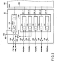
- Fig. 2 is a diagram schematically illustrating the power switch circuit used for the LSI device of the present embodiment.
- the power switch circuit 20 includes a first switch block 210 and a second switch block 290.
- the switch blocks 210 and 290 are connected between the power supply line 900 and an internal power supply line (also referred to as a virtual power supply line) 909 in a circuit block 190 in the CPU 10.
- an internal power supply line also referred to as a virtual power supply line
- elements and modules are connected to the internal power supply line 909.
- a plurality of internal power supply lines 909 may be provided in one circuit block 190.
- Each of the switch blocks 210 and 290 includes one or more switch cells SC arranged in parallel.
- Each of the switch cells SC includes one or more switch elements PSW.
- the switch element PSW is, for example, a P channel field-effect transistor (hereinafter referred to as a P-type transistor).
- a current path through the switch element PSW is connected between and in series with the power supply lines 900 and 909.
- the first switch block 210 can continuously supply the power supply voltage VDD to the circuit block 190 at a somewhat constant ramp-up speed when the supply of the power supply voltage to the circuit block 190 is started (for example, when the circuit block shifts from the off state to the on state).
- the first switch block 210 receives a first control signal PSW_ENa from an external control device 7.
- the first switch block 210 sets the switch element PSW to the on state or the off state based on the first control signal PSW_ENa.
- the first control signal PSW_ENa is supplied to the switch element (P-type transistor) PSW in the switch cell SC via an inverter 204.
- the control signal PSW_ENa may be generated in the CPU 10 based on the control by the external control device 7. At least one of the system controller 70 and the low power controller 79 generates the control signal PSW_ENa.
- the first switch block 210 outputs a notification signal PSW_ACK to the outside of the first switch block 210.
- the notification signal (completion notification signal) PSW_ACK is a signal indicating that control of the first switch block 210 (turn-on or -off of the switch element) has completed.
- the second switch block 290 includes a plurality of switch sections (switch groups) 291-1 to 291-5.
- a plurality of switch sections 291 is provided for one circuit block 190.
- the plurality of switch sections 291-1 to 291-5 is connected in parallel with each other between the power supply line 900 and the internal power supply line 909 in the circuit block 190.
- Each of the plurality of switch sections 291-1 to 291-5 includes one or more switch cells SC connected between the power supply line 900 and the internal power supply line 909.
- the second switch block 290 receives the notification signal PSW_ACK from the first switch block 210, for example, via the inverter 205.
- the notification signal PSW_ACK controls at least one of the plurality of switch sections 291-1 to 291-5.
- the power switch circuit 20 allows operations of the second switch block 290 (activation and inactivation) to be performed inside the CPU 10 in conjunction with operations of the first switch block 210 without the wait for the control from the external control device 7 based on the notification signal PSW_ACK.
- the second switch block 290 receives a plurality of second control signals PSW_ENb1 to PSW_ENb5 from the external control device 7.
- One of the plurality of second control signals PSW_ENb1 to PSW_ENb5 is supplied to one of the plurality of switch sections 291-1 to 291-5, for example, via a inverter 208.
- At least one of the system controller 70 and the low power controller 79 generates the control signals PSW_ENb1 to PSW_ENb5.
- the control signals PSW_ENb1 to PSW_ENb5 may be generated in the CPU 10 based on the control by the external control device 7.
- the plurality of switch sections 291-1 to 291-5 can be, for example, activated (on state) or inactivated (off state) at different timings in accordance with the plurality of control signals PSW_ENb1 to PSW_ENb5.
- the switch sections 291-1 to 291-5 are set to the on state at different timings.
- the switch sections 291-1 to 291-5 are set to the on state, current paths formed between the internal power supply line 909 and the power supply line 900 are formed in the switch sections 291-1 to 291-5.
- the independent switch sections 291 allow the power supply voltage (power) to be supplied to the internal power supply line 909 in the circuit block 190 in a time sharing manner (at different timings).
- how the power switch circuit 20, particularly the second switch block 290, is controlled can be adjusted and selectively controlled via software or firmware based on a user's specification, standards for the semiconductor system 800 to which the CPU 10 (LSI device 1) is applied, or the results of a test process for obtaining appropriate driving conditions for the LSI device 1.
- Control information (setting information) CI indicative of a control scheme for the power switch circuit 20 is, for example, stored in a memory area in the system controller 70 or the low power controller 79.
- the control information CI can be externally rewritten by the user via software (program) or firmware.
- the control information CI for the power switch circuit 20 may be stored in a memory circuit in the LSI device 1 or in a memory area in the CPU 10.
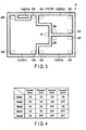
- Fig. 3 illustrates an example of an internal configuration (layout) of the CPU 10 included in the LSI device 1 of the present embodiment.
- a circuit in which a plurality of circuit blocks described below is provided may be a circuit other than the CPU.
- the CPU 10 includes a plurality of circuit blocks 100, 101, 102, and 103.
- Each of the circuit blocks 100 to 103 belong to different power supply systems (power supply shutdown area and voltage division area).
- circuit blocks belonging to different power supply systems are referred to as power domains.
- the power domain may be a circuit area with a certain logical function like a calculator such as an ALU, or a circuit area defined regardless of the logical function.
- Each of the power domains 100 to 103 have a circuit (element or module) and a function that allow processing of the CPU 10 to be executed.
- the power domain (PD0) 100 is a port area.
- the power domain 100 includes a plurality of ports.
- the ports include, for example, I/O ports (control ports) used for a retention flip flop circuit (hereinafter referred to as an RFF), a retention SRAM (hereinafter referred to as an RSRAM), a retention latch, an AOB (Always On Buffer), and an isolation cell.
- the I/O ports in the power domain 100 are used to receive and output a control signal for power-on and -off of cells such as an RFF and a control signal for management of the power-on and -off of the cells. It is also acceptable that the I/O ports for a retention circuit such as the RFF, the RSRAM, or a retention latch are not provided in the power domain 100.
- the RFF, the RSRAM, and the retention latch temporarily retain data such as the setting information for the CPU 10.
- the AOB is a buffer to which the power supply voltage is normally supplied so as to enable the control signal to be transmitted and received even when the power domain is in the off state.
- the isolation cell is a circuit that performs control so that an indefinite signal from the circuit switched from the off state to the on state (power domain) is prevented from propagating to another circuit.
- an I/O circuit such as a buffer circuit (not depicted in the drawings) is provided in the power domain 100.
- the I/O port is connected to an I/O circuit.
- Each of the power domains 101 to 103 includes a plurality of modules that allows a predetermined signal process and a predetermined calculation process to be executed.
- Each of power domains (PD1, PD2, and PD3) 101, 102, and 103 among the plurality of power domains executes a predetermined signal process and a predetermined calculation process according to the operating statuses of the semiconductor system and the LSI device 1.
- the power domain (PD1) 101 is a circuit block that can be set to an off state, for example, only when the power domains (PD2 and PD3) 102 and 103 are in the off state.
- the whole CPU 10 except for the I/O ports is set to the sleep state.
- the number of the power domains in the CPU 10 is not limited to four.
- a port area to which the power supply voltage VDD is normally applied may be provided inside the power domain 101, 102, or 103.
- the CPU 10 including the plurality of power domains 100 to 103 is driven in a plurality of operation modes according to the operating status of the semiconductor system 800 and the LSI device 1.
- the CPU 10 allows the power domains 100 to 103 on which no signal processing is executed to be set to the non-driven state (sleep mode) according to the operation mode of the CPU 10.
- Fig. 4 is a diagram illustrating an example of a correspondence between the operation mode of the CPU 10 and the operating state of each power domain.
- the CPU 10 is set to one of the operation modes that corresponds to the operating status of the semiconductor system.
- the operation mode of the CPU 10 is continually switched according to the operating status of the semiconductor system 800.
- the CPU 10 has five operation modes.
- Each of the power domains 100 to 103 is set to one of the on state (run state) and the off state (sleep state) according to the operation mode set for the CPU 10.
- the power domain (PD0) 100 provided with a port is set to the on state in all of the operation modes 1 to 5 in order to transmit and receive signals and to maintain the functions of the circuit.
- the three power domains 101 to 103 are set to the off state.
- one or more of the power domains 101 to 103 in which no signal processing is executed are set to the off state.
- the semiconductor system of the present embodiment allows only one power domain to be woken up or allows a plurality of power domains to be simultaneously woken up.
- controlling each of the power domains inside the CPU 10 enables the supply of the power supply voltage VDD to the CPU 10 to be controlled.
- the power switch circuit 20 supplies power to the power domain and shuts down the power supply to the power domain to control the off state and on state of each of the power domains 100 to 103.
- the power switch circuit 20 is provided in at least one of a boundary area 199 between the power domains 100 to 103 and an inside of the power domain 100 to 103. Consequently, the power domains 100 to 103 are separated from one another to allow turn-on and -off (supply of the power supply voltage) of the power domains 100 to 103 to be independently controlled.
- the power switch circuit 20 supplies the power supply voltage VDD to the power domains 100 to 103.
- the power switch circuit 20 electrically separates the power domains 100 to 103 from the power supply line 900 to shut down the supply of the power supply voltage VDD to the power domains 100 to 103.
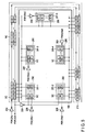
- Fig. 5 schematically depicts a configuration example of the power switch circuit in a certain power domain.
- the layout of the components depicted in Fig. 5 is schematically illustrated, and the present embodiment is not limited to the layout depicted in Fig. 5 .
- the power switch circuit 20 includes two types of switch blocks 210 and 290.
- the switch block 210 has a configuration and a control scheme both of which are referred to as a slew-rate control type
- the switch block 290 has a configuration and a control scheme both of which are referred to as a time-sharing control type.
- the first switch block 210 is referred to as the slew-rate control switch block 210
- the second switch block 290 is referred to as the time-sharing control switch block.
- the plurality of switch cells SC are, for example, arranged around the power domain 190 (101 to 103).
- the switch cells SC may be provided inside the power domain 190 as long as the switch cells SC enable design rules for the power domain 190 and the switch block 210 to be met, and enable the desired potential to be applied to the inside of the power domain 190.
- the switch cells SC are connected between the power supply line 900 and the internal power supply line 909 as current paths that connect the internal power supply line 909 to the power supply line 900.
- the plurality of switches SC is connected to a common control signal line.
- the switch cells SC connected to the common control signal line are also referred to as a switch string.
- the control signal PSW_ENa is supplied though a first end of the arranged switch cells (switch string) SC.
- the control signal PSW_ENa propagates on the control signal line from the one end of the arranged plurality of switch cells (a first end of the switch string) toward the other end of the arranged plurality of switch cells (a second end of the switch string).
- the control signal PSW_ENa having reached the other end of the switch string propagates on the control signal line in the opposite direction from the other end toward the one end of the switch string.
- a buffer, an inverter, and a repeater cell RC may be provided in the switch string so as to connect to the control signal line at predetermined intervals of the switch cells SC.
- Fig. 6 is an equivalent circuit diagram depicting a configuration example of switch cells in the power switch circuit in the present embodiment.
- Fig. 6 depicts an example of an internal configuration of switch cells in the slew-rate control switch block 210.
- the switch cells SC includes at least two types of switch elements WS1 and SS1 (PSW).
- One of the two switch elements, the switch element WS1, is hereinafter referred to as the weak switch WS1, and the other switch SS1 is hereinafter referred to as the strong switch SS1.
- a driving force for the P-type transistor WS1 serving as the weak switch WS1 is weaker than a driving force for the P-type transistor SS serving as the strong switch SS1.
- the element size (for example, the effective channel width/channel length) of the P-type transistor WS1 is smaller than the element size of the P-type transistor SS1.
- the strong switch SS1 with the strong driving force is turned on. This allows an internal voltage VDDV of the power domain to increase slowly.
- the weak switch WS1 and the strong switch SS1 are utilized to supply the power supply voltage VDD to the power domain 190, thus reducing a flow-through current(rush current) through the power domain 190 (and hard macros).
- the two P-type transistors WS1 and SS1 are connected together in parallel between the power supply line 900 and the internal power supply line 909.
- one of a source and a drain (for example, the source) of the P-type transistor WS1 is connected to the power supply line 900.
- the other of the source and drain (for example, the drain) of the P-type transistor WS1 is connected to the internal power supply line 909.
- one of a source and a drain (for example, the source) of the P-type transistor SS1 is connected to the power supply line 900.
- the other of the source and drain (for example, the drain) of the P-type transistor SS1 is connected to the internal power supply line 909.
- a gate of the P-type transistor WS1 is connected to a control signal line 950.
- a gate of the P-type transistor SS1 is connected to a control signal line 951.
- the control signal line 950 is connected to an output terminal of the inverter 204.
- the control signal line 950 is connected to the control signal line 951 via a buffer 952.
- a buffer 959 as the repeater cell RC is connected to the control signal lines 950 and 951.
- the buffer 959 reduces an excessive increase in signal delay to a value proportional to a line length.
- the slew-rate control switch block 210 includes two types of switch cells.
- Switch cells SC1 are different from switch cells SC2 in circuit configuration.
- the switch cell SC1 includes a capacitor (for example, a capacitor with a metal-oxide-metal structure) 954.
- the capacitor 954 is connected to the P-type transistor (weak switch) WS1.
- One end of the capacitor 954 is connected to the gate of the P-type transistor WS1, and the other end of the capacitor 954 is connected to the source/drain (in this case, the drain) of the P-type transistor on the power domain (virtual power supply line) side.
- Capacitive coupling of the capacitor 954 suppresses a decrease in the potential between the gate and drain resulting from an increase in the drain potential of the weak switch WS1. This allows adjustment of a ramp-up speed of the weak switch WS1.
- the switch cell SC2 includes no capacitor.
- the internal configuration of the switch cell SC2 is substantially the same as the internal configuration of the switch cell SC1 except for the absence of a capacitor.
- the switch cell SC1 with the capacitor 954 is provided on an input side for the control signal PSW_ENa (the first end of the switch string).
- the switch cell SC2 with no capacitor is arranged contiguously with the switch cell SC1 along an extending direction of the control signal lines 950 and 951.
- the control signal PSW_ENa output from the external control device 7 is supplied to a control terminal (gate of the transistor) for a switch of each switch cell SC to control turn-on and -off of the switch cell (switch element).
- the control signal PSW_ENa is hereinafter also referred to as the enable signal.
- the enable signal PSW_ENa propagates from the control signal line 950 to the control signal line 951 via the buffer 952.
- the buffer 952 amplifies the signal level.
- the weak switches WS1 are sequentially set to the on state from the switch cells SC1, located on the input side for the enable signal PSW_ENa, toward the switch cells SC2, located on the terminal of the switch block 210.
- the strong switches SS1 are sequentially set to the on state from the switch cells SC2, located on the terminal (buffer 952 side), toward the switch cells SC1, located on the input side for the enable signal (inverter 204 side).
- Each of the control signal lines 950 and 951 includes capacitive components and resistive components. At a speed corresponding to a time constant based on the capacitive components and the resistive components, the signal level of the enable signal PSW_ENa shifts from the H level to the L level. At a speed corresponding to the transition speed of the signal level, the P-type transistors WS1 and SS1, which serve as switch elements, gradually change from the off state to the on state.
- a current (drain current) with a magnitude corresponding to the driving forces and gate voltages of the P-type transistors WS1 and SS1 flows from the power supply line 900 to the internal power supply line 909 in the power domain 190 via the switch cells SC1 and SC2 to gradually increase the potential of the internal power supply line 909.
- the P-type transistors WS1 and SS1 are not in the complete on state, and output currents from the transistors WS1 and SS1 are relatively small.
- a current (the amount of current) flowing from the power supply line 900 to the internal power supply line 909 via the switch cells SC is small, suppressing the rush current.
- the capacitive components included in the control signal lines 950 and 951 are, for example, the capacitors 954 connected to the control signal lines 950 and 951 and the gate capacitances of the transistors WS1 and SS1 connected to the control signal lines 950 and 951 and line capacitances.
- the resistive components included in the control signal lines 950 and 951 are, for example, the on resistance of the transistors in the inverters or buffers connected to the control signal lines 950 and 951 and the line resistance.
- the number of the switch cells SC1 and SC2 in the slew-rate control switch block 210 corresponding to a certain power domain is set so as to set desired values (for example, values determined with the magnitude of the rush current and a startup period for the power domain taken into account) for a time constant that determines a transition speed for the signal levels of the control signal lines 950 and 951 (capacitive components and resistive components of the control signal lines), and a change speed for the potential VDDV of the internal power supply line in the power domain corresponding to the time constant.
- the switch elements WS1 and SS1 of the switch cells SC are gradually set to the on state to allow the switch cells SC to supply the internal power supply line 909 with drain currents with magnitudes corresponding to the driving states of the P-type transistors serving as the switch elements WS1 and SS1.
- the supply of the drain currents to the internal power supply line 909 results in charging of the internal power supply line 909, and the potential of the internal power supply line 909 increases in an analog manner (continuously) until the potential of the internal power supply line 909 becomes the same as the potential of the power supply line 900, that is, the VDDV.
- the above-described control of the switch elements WS1 and SS1 from the off state to the on state continuously starts up (turns on) the switches in the slew-rate control switch block 210 at a certain constant ramp-up speed and flattens currents generated by turn-on of the switches.
- the power switch circuit 20 including the slew-rate control switch block 210 allows a possible flow-through current to be suppressed.
- the slew-rate control switch block 210 outputs the notification signal PSW_ACK to the outside of the switch block 210 in association with the enable signal PSW_ENa.
- the notification signal PSW_ACK is a signal generated by outputting the enable signal PSW_ENa on the control signal line 951 via the inverter 953.
- the above-described circuit configuration and control scheme allows the slew-rate control switch block 210 to increase the internal voltage VDDV in the power domain 190 in an analog manner.
- a plurality of slew-rate control switch blocks 210 may be provided for one power domain 190.
- the plurality of slew-rate control switch blocks 210 uses different control signals (enable signals) to control the supply of power to the one power domain 190 (101 to 103) and the shutdown of the power.
- the plurality of slew-rate control switch blocks 210 may independently output the notification signal PSW_ACK.
- a plurality of switch strings controlled independently of one another function as a plurality of slew-rate control switch blocks 210.
- the time-sharing control switch block 290 includes the plurality of switch sections 291-1, 291-2, 291-3, 291-4, and 291-5.
- the switch sections 291-1 to 291-5 are distributively arranged inside the power domain 190.
- the switch sections 291-1 to 291-5 may be arranged in an outer peripheral area of the power domain 190 for which the supply of the power supply voltage VDD and the shutdown of the power are controlled (for example, in the boundary area 199 between the power domains).
- Fig. 5 illustrates an example in which the five switch sections 291-1 to 291-5 are provided.
- the number of switch sections in the time-sharing control switch block 290 may be four or less or six or more according to a circuit scale of the power domain 190.
- the switch sections 291-1 to 291-5 are controlled by control signals (enable signals) PSW_ENb1 to PSW_ENb5, respectively, from the external control device 7.
- Independent enable signals PSW_ENb1 to PSW_ENb5 are supplied to the switch sections 291-1 to 291-5, respectively.
- the time-sharing control switch block 290 may be controlled using, in addition to the enable signal PSW_ENa, the notification signal PSW_ACK from the slew-rate control switch block 210.
- the notification signal PSW_ACK from the slew-rate control switch block 210 is supplied to one or more of the plurality of switch sections 291.
- the notification signal PSW_ACK is supplied to the two switch sections 291-1 and 291-2. Besides the enable signals PSW_ENb1 and PSW_ENb2, the switch sections 291-1 and 291-2 use the notification signal PSW_ACK as a control signal for turn-on and -off of the switch cells (switch elements).
- the notification signal PSW_ACK is supplied to the switch sections 291-1 and 291-2 via the inverter 205.
- the configuration of the switch cells in the switch section may vary with the switch section.
- Fig. 7A and Fig. 7B are equivalent circuit diagrams depicting a configuration example of the switch cells in the power switch circuit.
- Fig. 7A and Fig. 7B depict an example of an internal configuration of the switch section 291 in the time-sharing control switch block 290.
- a switch cell SC3 like the switch cell in Fig. 6 , includes a weak switch WS2 and a strong switch SS2.
- a current path of the P-type transistor WS2 serving as the weak switch WS1 is connected between the power supply line 900 and the internal power supply line 909.
- a gate of the P-type transistor WS2 is connected to the control signal line 960.
- a current path of the P-type transistor SS2 serving as the strong switch SS2 is connected between the power supply line 900 and the internal power supply line 909.
- a gate of the P-type transistor SS2 is connected to the control signal line 961.
- the control signal line 961 is separated from the control signal line 960, and the two control signal lines 960 and 961 are independent of each other.
- the enable signal PSW_ENb1 is supplied to the gate of the P-type transistor WS2 serving as the weak switch WS2.
- the notification signal PSW_ACK is supplied to the gate of the P-type transistor SS2 serving as the strong switch SS2.
- turn-on and - off of the weak switch WS2 is controlled by the enable signal PSW_ENb1.
- Turn-on and -off of the strong switch SS2 may be controlled by the notification signal PSW_ACK.
- Fig. 7B depicts a switch cell configured differently from the switch cell in Fig. 7A .
- the time-sharing control switch block 290 may use a switch cell including one type of switch element.
- a switch cell SC4 does not include the weak switch and includes only a strong switch SS3.
- a current path of the P-type transistor SS3 serving as the strong switch SS3 is connected between the power supply line 900 and the internal power supply line 909.
- a gate of the P-type transistor SS3 is connected to a control signal line 970.
- the switch element in each of the switch cells SC3 and SC4 allows the internal power supply line 909 to be supplied with a current corresponding to the driving force and driving state of the P-type transistor serving as the switch element. Consequently, the internal power supply line 909 is charged to increase the potential of the internal power supply line 909.
- the number of switch cells in those of the plurality of switch sections 291 which are activated first is preferably smaller than the number of switch cells in the subsequently activated switch sections in order to suppress the rush current.
- the number of the switch cells in the switch section 291 increases in order of activation of the switch section.
- Switch cells with capacitors depicted in Fig. 6 may be used as the switch cells in the time-sharing control switch block 290.
- the above-described circuit configuration and control scheme allow the time-sharing control switch block 290 to, for example, digitally (discontinuously or discretely) increase the internal voltage VDDV of the power domain 190 based on the control by the plurality of switch sections 291.
- the plurality of switch sections 291 in the time-sharing control switch block 290 starts the supply of the power supply voltage VDD to the power domain 190 at different timings in parallel with the supply of the power supply voltage VDD by the slew-rate control switch block 210, based on the plurality of control signals PSW_ENb and the notification signal PSW_ACK.
- the time-sharing control switch block 290 may be operated in a supplementary manner for the supply of power by the slew-rate control switch block 210.
- the plurality of switch blocks 210 and 290 with the different control schemes performs power supply to increase the speed of the recovery operation of the circuit blocks.
- the power switch circuit 20 including the slew-rate control switch block 210 and the time-sharing control switch block 290 is not limited to the power switch circuit in the CPU 10.
- the power switch circuit 20 in Figs. 3 to 7 is applicable to a power switch circuit for the whole LSI device 1, or a power switch circuit in a circuit other than the CPU in the LSI device 1.
- Switch cells depicted in Fig. 6 , Fig. 7A, and Fig. 7B are illustrative. Switch cells other than the switch cells configured as depicted in Fig. 6 , Fig. 7A, and Fig. 7B may be used for the slew-rate control switch block 210 and the time-sharing control switch block 290.
- buffers or inverters may be connected to I/O terminals of the switch blocks 210 and 290 and the switch section 291 provided that the switch blocks 210 and 290 and the switch section 291 can perform predetermined control.
- the semiconductor system may fail to perform an amount of work (signal processing) per unit time, causing a malfunction of the system (breakdown of the system).
- an IR drop caused by an excessive rush current may occur in a circuit block to be woken up and in another circuit.
- a significant IR drop may cause malfunctioning of a circuit block switched from the off state to the on state or of a circuit other than that circuit block.
- the power switch circuit 20 in the LSI device of the present embodiment includes the plurality of switch blocks 210 and 290.
- the internal voltage of the circuit block is gradually increased so as not to cause a rush current.
- the internal voltage is rapidly increased to shorten the period of supply of the power supply voltage (power). In this manner, in the switch circuit 20 in the LSI device of the present embodiment, the two switch blocks 210 and 290 with the different control schemes for the supply of the power supply voltage, supply the power supply voltage to the circuit block 190 to be woken up.
- the power switch circuit 20 of the present embodiment allows the operating state of the circuit block to be switched from the off state to the on state at high speed, with an excessive rush current and an IR drop caused by the rush current suppressed.
- the LSI device including the power switch circuit of the present embodiment meets a demand for the shutdown of the power supply voltage expected for power saving while achieving operations required for the system, enabling a reduction in power consumption.
- the semiconductor integrated circuit of the present embodiment enables a reduction in the power consumption of the circuit (and the system) and thus an increase in the speed of operation.
- FIG. 8 and Fig. 9 an operation example (a method for controlling the LSI device) of the semiconductor integrated circuit of the present embodiment will be described.
- FIGs. 1 to 7 operations of the power switch circuit included in the semiconductor integrated circuit will be described.
- Fig. 8 is a timing chart illustrating the operation example of the LSI device of the present embodiment.
- Fig 8 illustrates timings for changes in control signals occurring when a certain power domain (circuit block) 190 in the CPU 10 returns from the off state (sleep state or non-driven state) to the on state (run state or driven state).
- the external control device 7 sets the enable signal (control signal) PSW_ENa or PSW_ENb to the L level.
- the slew-rate control switch block 210 and the time-sharing control switch block 290 when the L level enable signal PSW_ENa or PSW_ENb is supplied to the switch cells SC in Fig. 6 , Fig. 7A, and Fig. 7B , the signal level of the enable signal PSW_ENa or PSW_ENb is inverted from the L level to the H level by the inverter 204 or 208.
- the H level signals PSW_ENa and PSW_ENb turn off the switch elements WS1, WS2, SS1, and SS3 of the P-type transistor.
- the slew-rate control switch block 210 is in the non-driven state, and thus the signal level of the notification signal PSW_ACK is the L level.
- the switch SS2 of the P-type transistor is in the off state.
- the switch elements WS and SS in the off state electrically separate the power domain 190 from the power supply line 900 to set the power domain 190 to the off state.
- the operation mode of at least one power domain 190 shifts from the off state to the on state (wakes up).
- the external control device 7 controls the signal level of the enable signal PSW_ENa or PSW_ENb for the power switch circuit 20 corresponding to the power domain 190 to be woken up.
- the power switch circuit 20 starts supplying the power supply voltage VDD to the power domain 190 in the off state.
- the external control device 7 asserts the enable signal PSW_ENa for the slew-rate control switch block 210.
- the signal level of the enable signal PSW_ENa shifts from the L level to H level at a point in time (time instant) ta.
- the signal level of the enable signal PSW_ENa is inverted by the inverter 204.
- the L level enable signal PSW_ENa is supplied to each of the switch cells SC1 and SC2 via the control signal line 950. Consequently, the weak switch WS1 of the two switch elements in the switch cell SC is turned on.
- the strong switch SS1 is turned on by the L level enable signal PSW_ENa on the control signal line 951.
- the supply of the power supply voltage VDD by the slew-rate control switch block 210 increases the internal voltage VDDV of the power domain 190 at a speed corresponding to the ramp-up speed based on the characteristics of the plurality of switch elements WS1 and SS1 (time constant and driving power). As a result, the generation of a current in the power domain is flattened to suppress an excessive large flow-through current.
- the time-sharing control switch block 290 After the enable signal PSW_ENa is asserted, the plurality of enable signals PSW_ENb for the time-sharing control switch block 290 is asserted, for example, by the external control device 7. Consequently, in parallel with the supply of the power supply voltage VDD by the slew-rate control switch block 210, the time-sharing control switch block 290 starts supplying the power supply voltage VDD to the power domain 190 to be woken up.
- the signal levels of the plurality of enable signals PSW_ENb1 to PSW_ENb5 shifts from the L level to the H level at different timings (points in time tb1 to tb5). Consequently, the plurality of switch sections is sequentially set to the on state.
- the enable signal PSW_ENb1 shifts from the L level to the H level.
- the enable signal PSW_ENb2 is set to the H level.
- the L level signals PSW_ENb1 and PSW_ENb2 are supplied via the inverter 208 to the switch cells SC3 in the switch sections 291-1 and 291-2 at different timings.
- the switch cells SC3 in the switch sections 291-1 and 291-2 includes the weak switch WS2 and the strong switch SS2.
- the switch turned on by the enable signal PSW_ENb1 and PSW_ENb2 is the weak switch WS2.
- the strong switch SS2 is a switch element controlled by the notification signal PSW_ACK. Thus, the strong switch SS1 is not turned on at point in time tb1 or tb2.
- the enable signal PSW_ENb3 is set to the H level.
- the signal level of the enable signal PSW_ENa is inverted by the inverter 208, and the L level signal is supplied to the switch cell SC4 in the switch section 291-3.
- the switch cell SC4 includes no weak switch.
- the strong switch SS3 is controlled by the enable signal PSW_ENb3. Therefore, the enable signal PSW_ENb3 turns on the strong switch SS3.
- the enable signal PSW_ENb4 is set to the H level.
- the enable signal PSW_ENb5 is set to the H level.
- the enable signals PSW_ENb4 and PSW_ENb5 respectively are sequentially supplied to the switch sections 291-4 and 291-5 with the signal levels thereof inverted from the H level to the L level.
- the switch cells SC3 in the switch sections 291-4 and 291-5 include no weak switch. Therefore, the enable signals PSW_ENb4 and PSW_ENb5 turn on the strong switches SS3 in the switch sections 291-4 and 291-5 at different timings.
- the notification signal PSW_ACK is at the L level. Therefore, when the strong switches SS3 in the switch sections 291-3 to 291-5 are turned on, the strong switches SS1 in the switch sections 291-1 and 291-2 are in the off state.
- the slew-rate control switch block 210 After the asserted enable signal PSW_ENb is supplied to the switch section 291 in the time-sharing control switch block 290, at point in time tz, the slew-rate control switch block 210, having completed turn-on of the switch elements, outputs the asserted notification signal PSW_ACK.
- the signal level of the notification signal PSW_ACK shifts from the L level to the H level.
- the timing for the output of the asserted notification signal PSW_ACK is preset by firmware (and software) for the external control device 7 or a delay circuit added to the switch block 290.
- the H level notification signal PSW_ACK is output from the slew-rate control switch block 210.
- the notification signal PSW_ACK is supplied to the external control device 7 and to the time-sharing control switch block 290.
- the signal level of the notification signal PSW_ACK is inverted from the H level to the L level by the inverter 205, and the L level signal PSW_ACK is supplied to the strong switches SS2 in the switch sections 291-1 and 291-2. Consequently, the strong switches SS2 in the switch sections 291-1 and 291-2 are turned on.
- the switch sections 291 in the time-sharing control switch block 290 are activated at temporally divided timings (at different timings).
- the switch sections 291 independently start and execute the supply of the power supply voltage to the power domain with a plurality of switch sections.
- the power domain is powered on (for example, at or after point in time tz), and then, the external control device 7 transmits, for example, a control signal allowing recovery from the sleep state to the CPU 10.
- the control of the power switch circuit 20 included in the LSI device of the present embodiment is completed by the control signals PSW_ENa and PSW_ENb from the external control device 7 and the notification signal PSW_ACK generated inside the power switch circuit 20. Consequently, the power supply voltage is supplied to the power domain via the power switch circuit 20.
- the switch blocks 210 and 290 are set to the off state (inactivated state) at a time by the control signals PSW_ENa and PSW_ENb.
- the wakeup operation for one power domain has been described. However, the above-described operation may allow the wakeup operation to be simultaneously performed on the plurality of power domains 101 to 103 at the same time.
- each of the times (time instants) ta, tb1 to tb5 and tz represents a value from a starting point (for example, a start of the wakeup operation) to a transition point of signal level of the control signal.
- each of the times ta, tb1 to tb5 and tz is preset based on at least one of a design rule and a result of a test process.
- Each of the times ta, tb1 to tb5 and tz may be dynamically changes based on the monitoring result of the potential of the internal power supply line during the wakeup operation.
- Fig. 9 is a diagram depicting changes in the internal voltage of the power domain during the recovery operation in the present operation example.
- the horizontal axis corresponds to time, and the vertical axis corresponds to the internal voltage (potential of the virtual power supply line) VDDV of the power domain.
- a solid line L1 represents changes in the internal voltage of the power domain during the recovery operation performed by the power switch circuit of the present embodiment.
- a dashed line L2 represents, as a comparative example, changes in the internal voltage of the power domain during a recovery operation performed by an LSI device using a power switch circuit including only a slew-rate control switch block.
- the slew-rate control switch block 210 starts supplying a voltage.
- the switch sections 291 in the time-sharing control switch block 290 are sequentially set to the on state.
- a current from the switch section 291 in the on state is supplied to the internal power supply line 909 separately from a current from the slew-rate control switch block 210.
- the additional charging of the internal power supply line 909 by the switch section 291 increases the rate of increase in the internal voltage VDDV at the timing when the switch section 291 is turned on in comparison to the rate of increase in potential when power is supplied only by the slew-rate control switch block 210.
- the time for the internal voltage VDDV of the power domain to reach a target voltage value can be shortened. Consequently, the amount of time until the start of driving of the power domain to be woken up (the amount of time to switch the power domain from the off state to the on state) is reduced.
- the slew-rate control switch block 210 changes the internal voltage in an analog manner
- the time-sharing control switch block 290 also changes the internal voltage VDDV in a supplementary manner.
- the internal voltage increases under the control of the slew-rate control switch block 210. Therefore, in the present embodiment, when the operating state of the power domain 190 switches from the off state to the on state, no excessive rush current is generated.
- the method for controlling the power switch circuit 20 in the LSI device of the present embodiment allows the power domain 190 to be switched from the off state to the on state for restarting, in the condition where the occurrence of an excessive rush current and the overhead of the processing time, which is caused by the time to switch the circuit block between the on state and the off state, are suppressed.
- the LSI device of the present embodiment enables a reduction in power consumption and an increase in the speed of the device.
- the power switch circuit includes two switch blocks based on different control schemes to allow a control scheme (a scheme in which a power supply voltage is supplied to a power domain) for the power switch circuit 20 to be changed in accordance with a user's specifications and standards for the LSI/system.
- a control scheme a scheme in which a power supply voltage is supplied to a power domain
- Control information CI in the external control device 7 is rewritten by software or firmware to change the control scheme for the power switch circuit 20.
- a timing for assertion of an enable signal indicated in the control information CI is changed to enable a change in a scheme in which the power supply voltage is supplied to the power domain, using the same circuit configuration as that in the first embodiment.
- time-sharing control switch block 290 may be controlled using only the control signal PSW_ENb from the external control device 7 in accordance with the user's specifications and the standards applied to the semiconductor system.
- the LSI device of the present embodiment allows the supply of the power supply voltage to the power domain to be controlled without depending on the supply of power by the time-sharing control switch block 290, and using only the slew-rate control switch block 210.
- Fig. 10 is a timing chart illustrating the operation example of the LSI device of the present embodiment.
- Fig. 10 illustrates timings for changes in control signals in the power switch circuit.
- the operation of the power switch circuit 20 can be changed by changing the control information CI for the power switch circuit 20 via software (or firmware) in accordance with the user's specifications and the LSI standards.
- the time-sharing control switch block 290 in the power switch circuit 20 allows the plurality of switch sections 291 to be set to the on state at a time by changing the control scheme via software in accordance with the user's specifications and the LSI standards.
- the external control device 7 shifts the enable signal PSW_ENa for the slew-rate control switch block 210 from the L level to the H level.
- the slew-rate control switch block 210 When the operation in the switch block 210 is complete, the slew-rate control switch block 210 outputs the H level notification signal PSW_ACK.
- the external control device 7 shifts the enable signals PSW_ENb for the time-sharing control switch block 290 from the L level to the H level at substantially the same timing.
- the signal levels of the enable signals PSW_ENb are set to the H level in synchronism with the timing when the notification signal PSW_ACK is set to the H level.
- the timing when the signal levels of the enable signals PSW_ENb are set to the H level may be different from the timing when the notification signal PSW_ACK is set to the H level.
- such control of the time-sharing control switch block 290 that sets the plurality of switch sections 291 to the on state at one time does not depend on the notification signal PSW_ACK from the slew-rate control switch block 210.
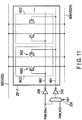
- Fig. 11 is an equivalent circuit diagram depicting a modification example of the power switch circuit in the present embodiment.
- a selector 209 to which the enable signal PSW_ENb and the notification signal PSW_ACK are supplied may be connected to an input section of the control signal line 961 (for example, connected to an upstream side of the inverter 205).
- the external control device 7 supplies a control signal (select signal) CNT to the selector 209.
- the selector selects one of the enable signal PSW_ENb1 and the notification signal PSW_ACK.
- the above-described operation allows the power supply voltage VDD to be supplied to the power domain 190 (101 to 103) via the power switch circuit 20.
- the LSI device of the present embodiment enables an operation of the LSI device different from the operation in Fig. 10 , as depicted in Fig. 12 .
- Fig. 12 is a timing chart illustrating an operation example of the LSI device of the present embodiment.
- Fig. 12 depicts timings for changes in control signals in the power switch circuit.
- Driving of the slew-rate control switch block 210 may be started after driving of the time-sharing control switch block 290 is started.
- Such a method for controlling the power switch circuit 20 may be changed by allowing the external control device 7 to rewrite the control information CI using software (or firmware).
- the signal levels of the plurality of enable signals PSW_ENb1 to PSW_ENb5 are sequentially set to the H level.
- the plurality of switch sections 291 are sequentially activated at different timings.
- the power domain 190 is made electrically continuous with the power supply line 900 via the time-sharing control switch block 290 in the on state.
- the switch sections start supplying the power supply voltage (power) at different timings.
- the enable signal PSW_ENb is set to the H level.
- the enable signal PSW_ENa is set to the H level substantially simultaneously with the timing when the enable signal PSW_ENb5 is set to the H level.
- the weak switch WS1 and the strong switch SS1 in the slew-rate control switch block 210 are sequentially activated. Consequently, the power domain 190 is made electrically continuous with the power supply line 900 via the slew-rate control switch block 210 in the on state.
- the slew-rate control switch block 210 starts supplying the power supply voltage VDD.
- the strong switches SS2 in the time-sharing control switch block 290 are activated.
- the above-described operation allows the power supply voltage VDD to be supplied to the power domain via the power switch circuit 20.
- the CPU and LSI device including the power switch circuit 20 driven by the operation illustrated in Fig. 12 produces effects substantially similar to the effects of the control (the operation of recovering the power domain) of the power switch circuit 20 driven by the operation illustrated in Fig. 8 .
- Fig. 13 is a timing chart illustrating an operation example of the LSI device of the present embodiment.
- Fig. 13 illustrates timings for change in control signals in the power switch circuit.
- some of the switch elements in the power switch circuit 20 may be maintained in the on state as depicted in Fig. 13 .
- the enable signal PSW_ENb1 is normally set to the H level, with the switch elements in the switch section 291-1 set to the on state.
- the enable signals PSW_ENa, and PSW_ENb2 to PSW_ENB5 are set to the L level in the off state of the power domain, the switch elements corresponding to the enable signals PSW_ENa and PSW_ENb2 set to the off state. And then, when the power domain is recovered from the sleep state, the signal levels of the enable signals PSW_ENa and PSW_ENb2 to PSW_ENB5 are shifted from L level to H level in order.
- the switch elements in the on state allows low power (for example, a small current) to be supplied, during a sleep operation, to the internal power supply line 909 through the power supply line 900, the internal power supply line 909 is weakly charged to the extent that the power domain 190 is not driven.
- the present embodiment allows the CPU and LSI device including the power switch circuit 20 driven by the operation illustrated in Fig. 13 to achieve an operation of quickly recovering (waking up) the power domain 190.
- the number of switch elements (switch sections) set to the on state in the sleep state is smaller than the number of switch elements set to the off state, so as to prevent the power domain 190 from being driven during the sleep.
- the number of switch elements set to the on state in the sleep state is preferably set so as to achieve a reduction in the power consumption in the power domain 190.
- Fig. 13 illustrates an example of a method for controlling the power switch circuit 20 depicted in Fig. 8 in which some of the switch elements (switch sections) are on while the power domain 190 is in the off state.
- some of the switch elements (switch sections) may be turned on while the power domain 190 is sleeping in order to achieve an operation of quickly recovering the power domain 190.
- control information CI for the power switch circuit 20 is rewritten via software, the operation of the power switch circuit 20, including the switch block 210 and 290 based on the different control schemes, can be flexibly changed in accordance with the user's specifications or the standards/design for the LSI device, without the need to significantly change the internal configuration of the power switch circuit 20.
- the LSI device of the present embodiment enables the enhancement of flexibility of design for system LSI, a reduction in design period for the LSI device and the semiconductor system, and a reduction in manufacturing costs for the LSI device and the semiconductor system.
- the switch circuit 20 included in the semiconductor integrated circuit in the above-described embodiments is applicable to devices other than the CPU, for example, an image sensor and a semiconductor memory.
Landscapes
- Engineering & Computer Science (AREA)
- General Engineering & Computer Science (AREA)
- Theoretical Computer Science (AREA)
- Physics & Mathematics (AREA)
- Computer Hardware Design (AREA)
- Computing Systems (AREA)
- General Physics & Mathematics (AREA)
- Mathematical Physics (AREA)
- Semiconductor Integrated Circuits (AREA)
- Logic Circuits (AREA)
- Electronic Switches (AREA)
Claims (8)
- Halbleiterbauelement, das Folgendes umfasst:eine Spannungsleitung (900), an die eine erste Spannung angelegt ist;eine erste Schaltung (10), die konfiguriert ist, um durch Verwenden der ersten Spannung zu arbeiten; undeine zweite Schaltung (20), die konfiguriert ist, um eine Verbindung zwischen der Spannungsleitung und der ersten Schaltung zu steuern;wobei die zweite Schaltung Folgendes beinhaltet:mindestens einen ersten Schaltkreis (210), der eine Vielzahl erster Schaltzellen (SC) beinhaltet; undeinen zweiten Schaltkreis (290), der eine Vielzahl von Schaltabschnitten (291-1 bis 291-5) beinhaltet,wobei die Vielzahl erster Schaltzellen konfiguriert ist, um die erste Schaltung und die Spannungsleitung basierend auf einem ersten Steuersignal (PSW_ENa) zu verbinden,wobei die Vielzahl von Schaltabschnitten konfiguriert ist, um die erste Schaltung und die Spannungsleitung basierend auf einer Vielzahl zweiter Steuersignale (PSW_ENb1 bis PSW_ENb5), die von dem ersten Steuersignal unterschiedlich sind, zu verbinden,wobei jedes der Vielzahl zweiter Steuersignale zu unterschiedlichen Zeiten bestätigt wird,wobei der erste Schaltkreis ein verzögertes Signal (PSW_ACK) des ersten Steuersignals ausgibt, nachdem die Vielzahl erster Schaltzellen sequenziell eingeschaltet wurde,jeder der Vielzahl von Schaltabschnitten auf einen Zustand zu unterschiedlichen Zeitpunkten basierend auf der Vielzahl zweiter Steuersignale eingestellt ist, undein erster Schaltabschnitt (291-1) der Vielzahl von Schaltabschnitten basierend auf dem verzögerten Signal und einem ersten Signal (PSW_ENb1) der Vielzahl zweiter Steuersignale eingeschaltet wird, dadurch gekennzeichnet, dass das verzögerte Signal angibt, dass die Verbindung zwischen der ersten Schaltung und der Spannungsleitung über den ersten Schaltkreis abgeschlossen ist, da sie das Einschalten der Schaltelemente in dem ersten Schaltkreis abgeschlossen hat.
- Halbleiterbauelement nach Anspruch 1, wobei der erste Schaltkreis das verzögerte Signal basierend auf dem ersten Steuersignal erzeugt.
- Halbleiterbauelement nach Anspruch 1, wobei, während einer Periode, wenn die erste Schaltung auf einen Nicht-Betriebszustand gestellt ist,
der erste Schaltkreis ausgeschaltet ist, und
mindestens einer der Vielzahl von Schaltabschnitten eingeschaltet ist, und die restlichen Schaltabschnitte ausgeschaltet sind. - Halbleiterbauelement nach Anspruch 1, wobei der erste Schaltkreis eine erste Schaltzelle beinhaltet, und
mindestens eine der Vielzahl erster Schaltzellen ein erstes Schaltelement und ein zweites Schaltelement beinhaltet, das von dem ersten Steuersignal gesteuert wird,
das zweite Schaltelement eingeschaltet wird, nachdem das erste Schaltelement eingeschaltet wurde, und
eine Ansteuerkraft des zweiten Schaltelements größer ist als eine Ansteuerkraft des ersten Schaltelements. - Halbleiterbauelement nach Anspruch 1, wobei der erste Schaltabschnitt mindestens eine zweite Schaltzelle beinhaltet,
die zweite Schaltzelle ein drittes Schaltelement beinhaltet, das von dem ersten Signal gesteuert wird, und ein viertes Schaltelement, das von dem verzögerten Signal gesteuert wird, und
das vierte Schaltelement eingeschaltet wird, nachdem das dritte Schaltelement eingeschaltet wurde, und
eine Ansteuerkraft des vierten Schaltelements größer ist als eine Ansteuerkraft des dritten Schaltelements. - Halbleiterbauelement nach Anspruch 1, wobei
der erste Schaltabschnitt mindestens eine zweite Schaltzelle beinhaltet,
ein zweiter Schaltabschnitt der Vielzahl von Schaltabschnitten mindestens eine dritte Schaltzelle beinhaltet,
die Vielzahl der ersten Schaltzellen sequenziell in einer ersten Periode von einem ersten Zeitpunkt bis zu einem zweiten Zeitpunkt eingeschaltet wird,
die zweite Schaltzelle in einem dritten Zeitpunkt eingeschaltet wird, der von dem ersten und zweiten Zeitpunkt in der ersten Periode unterschiedlich ist, und
die dritte Schaltzelle in einem vierten Zeitpunkt eingeschaltet wird, der von dem ersten, zweiten und dritten Zeitpunkt in der ersten Periode unterschiedlich ist. - Halbleiterbauelement nach Anspruch 1, das weiter Folgendes umfasst:einen Controller (7), der konfiguriert ist, um die zweite Schaltung zu steuern,wobei der Controller das erste Steuersignal und die Vielzahl zweiter Steuersignale zu der zweiten Schaltung ausgibt.
- Halbleiterbauelement nach Anspruch 7, wobei der Controller Steuerinformation beinhaltet, um den ersten und den zweiten Schaltkreis zu steuern.
Applications Claiming Priority (1)
| Application Number | Priority Date | Filing Date | Title |
|---|---|---|---|
| JP2014259422A JP6320290B2 (ja) | 2014-12-22 | 2014-12-22 | 半導体集積回路 |
Publications (3)
| Publication Number | Publication Date |
|---|---|
| EP3046258A2 EP3046258A2 (de) | 2016-07-20 |
| EP3046258A3 EP3046258A3 (de) | 2016-10-12 |
| EP3046258B1 true EP3046258B1 (de) | 2020-06-03 |
Family
ID=54146955
Family Applications (1)
| Application Number | Title | Priority Date | Filing Date |
|---|---|---|---|
| EP15184047.7A Active EP3046258B1 (de) | 2014-12-22 | 2015-09-07 | Halbleiterbauelement |
Country Status (5)
| Country | Link |
|---|---|
| US (1) | US9608625B2 (de) |
| EP (1) | EP3046258B1 (de) |
| JP (1) | JP6320290B2 (de) |
| CN (1) | CN105718021B (de) |
| TW (1) | TWI596902B (de) |
Families Citing this family (2)
| Publication number | Priority date | Publication date | Assignee | Title |
|---|---|---|---|---|
| JP6602278B2 (ja) * | 2016-09-16 | 2019-11-06 | 株式会社東芝 | 半導体装置 |
| JP2023183889A (ja) * | 2022-06-17 | 2023-12-28 | キオクシア株式会社 | 半導体集積回路 |
Citations (1)
| Publication number | Priority date | Publication date | Assignee | Title |
|---|---|---|---|---|
| US20130002339A1 (en) * | 2011-06-29 | 2013-01-03 | Suganth Paul | Low-power, low-latency power-gate apparatus and method |
Family Cites Families (18)
| Publication number | Priority date | Publication date | Assignee | Title |
|---|---|---|---|---|
| JP4967532B2 (ja) * | 2006-08-25 | 2012-07-04 | 富士通セミコンダクター株式会社 | 半導体集積回路および半導体集積回路のテスト方法 |
| CN101765973A (zh) * | 2007-09-27 | 2010-06-30 | 松下电器产业株式会社 | 半导体集成电路装置、通信装置、信息再生装置、图像显示装置、电子装置、电子控制装置以及移动体 |
| US7977822B2 (en) * | 2007-11-05 | 2011-07-12 | Arm Limited | Dynamically changing control of sequenced power gating |
| US7586325B1 (en) | 2007-12-03 | 2009-09-08 | Lattice Semiconductor Corporation | Integrated circuit having independent voltage and process/temperature control |
| JP2009151573A (ja) | 2007-12-20 | 2009-07-09 | Fujitsu Microelectronics Ltd | 半導体集積回路 |
| JP4535134B2 (ja) * | 2008-01-16 | 2010-09-01 | ソニー株式会社 | 半導体集積回路およびその電源制御方法 |
| JP2009264948A (ja) * | 2008-04-25 | 2009-11-12 | Sony Corp | 半導体装置 |
| JP2010093318A (ja) * | 2008-10-03 | 2010-04-22 | Panasonic Corp | 半導体集積回路及びlsiシステム |
| JP2010258267A (ja) | 2009-04-27 | 2010-11-11 | Toshiba Corp | 半導体集積装置 |
| JP2011243794A (ja) | 2010-05-19 | 2011-12-01 | Renesas Electronics Corp | 半導体装置、電源スイッチの制御方法及びその設計方法 |
| JP5576248B2 (ja) * | 2010-11-19 | 2014-08-20 | ルネサスエレクトロニクス株式会社 | 電源スイッチ回路 |
| JP5714924B2 (ja) * | 2011-01-28 | 2015-05-07 | ラピスセミコンダクタ株式会社 | 電圧識別装置及び時計制御装置 |
| JP5163761B2 (ja) * | 2011-02-09 | 2013-03-13 | 富士ゼロックス株式会社 | 電力供給制御装置、画像処理装置、電力供給制御プログラム |
| JP2012248674A (ja) * | 2011-05-27 | 2012-12-13 | Renesas Electronics Corp | 半導体集積回路 |
| JP2013125774A (ja) * | 2011-12-13 | 2013-06-24 | Toshiba Corp | 半導体集積回路装置 |
| KR102022355B1 (ko) | 2012-07-10 | 2019-09-18 | 삼성전자주식회사 | 파워 게이팅 회로 |
| FR2999832A1 (fr) * | 2012-12-14 | 2014-06-20 | St Microelectronics Sa | Procede et dispositif de gestion d'une mise sous tension d'un domaine d'un circuit electronique |
| JP2015053612A (ja) * | 2013-09-06 | 2015-03-19 | 株式会社東芝 | 半導体集積回路 |
-
2014
- 2014-12-22 JP JP2014259422A patent/JP6320290B2/ja active Active
-
2015
- 2015-09-03 US US14/845,138 patent/US9608625B2/en active Active
- 2015-09-07 EP EP15184047.7A patent/EP3046258B1/de active Active
- 2015-12-01 TW TW104140212A patent/TWI596902B/zh active
- 2015-12-18 CN CN201510959074.2A patent/CN105718021B/zh active Active
Patent Citations (1)
| Publication number | Priority date | Publication date | Assignee | Title |
|---|---|---|---|---|
| US20130002339A1 (en) * | 2011-06-29 | 2013-01-03 | Suganth Paul | Low-power, low-latency power-gate apparatus and method |
Also Published As
| Publication number | Publication date |
|---|---|
| EP3046258A3 (de) | 2016-10-12 |
| CN105718021B (zh) | 2019-03-12 |
| US20160182041A1 (en) | 2016-06-23 |
| EP3046258A2 (de) | 2016-07-20 |
| JP6320290B2 (ja) | 2018-05-09 |
| TW201635704A (zh) | 2016-10-01 |
| CN105718021A (zh) | 2016-06-29 |
| JP2016119422A (ja) | 2016-06-30 |
| US9608625B2 (en) | 2017-03-28 |
| TWI596902B (zh) | 2017-08-21 |
Similar Documents
| Publication | Publication Date | Title |
|---|---|---|
| JP6113930B2 (ja) | 供給電圧バイアス回路によるスタティックランダムアクセスメモリ(sram)における耐プロセス電流リーケージ低減 | |
| JP6026191B2 (ja) | 電力制御回路、それを含む半導体装置及び該電力制御回路の動作方法 | |
| US9720434B2 (en) | Power gating in an electronic device | |
| KR20170116042A (ko) | 독립적인 전력 콜랩스 방법론 | |
| EP3132327B1 (de) | Schaltbare entkopplungskondensatoren | |
| CN101304250B (zh) | 半导体集成电路及其操作方法 | |
| KR20070047645A (ko) | 클럭 드라이버 | |
| KR20180026781A (ko) | 집적 회로용 전력 멀티플렉서 | |
| JP2010515277A (ja) | インラッシュ制限用電力アイランドを有するシステム、方法、および集積回路 | |
| US8723592B2 (en) | Adjustable body bias circuit | |
| US9425792B2 (en) | Reconfigurable power switch chains for efficient dynamic power saving | |
| EP3046258B1 (de) | Halbleiterbauelement | |
| JP5333219B2 (ja) | 半導体集積回路 | |
| JP5278167B2 (ja) | 半導体集積回路装置及び電源システム | |
| US9854531B2 (en) | Integrated circuit system and integrated circuit | |
| US20120206186A1 (en) | Output circuit, system including output circuit, and method of controlling output circuit | |
| JP2014038382A (ja) | 半導体装置とその電源制御方法 | |
| TW202024843A (zh) | 電子裝置以及供電方法 | |
| CN103684421A (zh) | 电路装置 | |
| US20160036439A1 (en) | Semiconductor integrated circuit device | |
| US8199601B2 (en) | System and method of selectively varying supply voltage without level shifting data signals | |
| US20110234297A1 (en) | Semiconductor integrated circuit and its control technique | |
| US9483100B2 (en) | Method and apparatus for power gating hardware components in a chip device | |
| US10804903B1 (en) | Asynchronous circuit stacking for simplified power management | |
| JP7801017B2 (ja) | 低オーバーヘッド広帯域幅再構成可能な相互接続装置及び方法 |
Legal Events
| Date | Code | Title | Description |
|---|---|---|---|
| PUAI | Public reference made under article 153(3) epc to a published international application that has entered the european phase |
Free format text: ORIGINAL CODE: 0009012 |
|
| 17P | Request for examination filed |
Effective date: 20150907 |
|
| AK | Designated contracting states |
Kind code of ref document: A2 Designated state(s): AL AT BE BG CH CY CZ DE DK EE ES FI FR GB GR HR HU IE IS IT LI LT LU LV MC MK MT NL NO PL PT RO RS SE SI SK SM TR |
|
| AX | Request for extension of the european patent |
Extension state: BA ME |
|
| PUAL | Search report despatched |
Free format text: ORIGINAL CODE: 0009013 |
|
| AK | Designated contracting states |
Kind code of ref document: A3 Designated state(s): AL AT BE BG CH CY CZ DE DK EE ES FI FR GB GR HR HU IE IS IT LI LT LU LV MC MK MT NL NO PL PT RO RS SE SI SK SM TR |
|
| AX | Request for extension of the european patent |
Extension state: BA ME |
|
| RIC1 | Information provided on ipc code assigned before grant |
Ipc: G06F 1/32 20060101ALI20160907BHEP Ipc: H03K 19/00 20060101AFI20160907BHEP |
|
| STAA | Information on the status of an ep patent application or granted ep patent |
Free format text: STATUS: EXAMINATION IS IN PROGRESS |
|
| 17Q | First examination report despatched |
Effective date: 20181116 |
|
| GRAP | Despatch of communication of intention to grant a patent |
Free format text: ORIGINAL CODE: EPIDOSNIGR1 |
|
| STAA | Information on the status of an ep patent application or granted ep patent |
Free format text: STATUS: GRANT OF PATENT IS INTENDED |
|
| INTG | Intention to grant announced |
Effective date: 20200109 |
|
| GRAS | Grant fee paid |
Free format text: ORIGINAL CODE: EPIDOSNIGR3 |
|
| GRAA | (expected) grant |
Free format text: ORIGINAL CODE: 0009210 |
|
| STAA | Information on the status of an ep patent application or granted ep patent |
Free format text: STATUS: THE PATENT HAS BEEN GRANTED |
|
| AK | Designated contracting states |
Kind code of ref document: B1 Designated state(s): AL AT BE BG CH CY CZ DE DK EE ES FI FR GB GR HR HU IE IS IT LI LT LU LV MC MK MT NL NO PL PT RO RS SE SI SK SM TR |
|
| REG | Reference to a national code |
Ref country code: GB Ref legal event code: FG4D |
|
| REG | Reference to a national code |
Ref country code: CH Ref legal event code: EP Ref country code: AT Ref legal event code: REF Ref document number: 1278092 Country of ref document: AT Kind code of ref document: T Effective date: 20200615 |
|
| REG | Reference to a national code |
Ref country code: DE Ref legal event code: R096 Ref document number: 602015053658 Country of ref document: DE |
|
| REG | Reference to a national code |
Ref country code: LT Ref legal event code: MG4D |
|
| PG25 | Lapsed in a contracting state [announced via postgrant information from national office to epo] |
Ref country code: SE Free format text: LAPSE BECAUSE OF FAILURE TO SUBMIT A TRANSLATION OF THE DESCRIPTION OR TO PAY THE FEE WITHIN THE PRESCRIBED TIME-LIMIT Effective date: 20200603 Ref country code: LT Free format text: LAPSE BECAUSE OF FAILURE TO SUBMIT A TRANSLATION OF THE DESCRIPTION OR TO PAY THE FEE WITHIN THE PRESCRIBED TIME-LIMIT Effective date: 20200603 Ref country code: NO Free format text: LAPSE BECAUSE OF FAILURE TO SUBMIT A TRANSLATION OF THE DESCRIPTION OR TO PAY THE FEE WITHIN THE PRESCRIBED TIME-LIMIT Effective date: 20200903 Ref country code: GR Free format text: LAPSE BECAUSE OF FAILURE TO SUBMIT A TRANSLATION OF THE DESCRIPTION OR TO PAY THE FEE WITHIN THE PRESCRIBED TIME-LIMIT Effective date: 20200904 Ref country code: FI Free format text: LAPSE BECAUSE OF FAILURE TO SUBMIT A TRANSLATION OF THE DESCRIPTION OR TO PAY THE FEE WITHIN THE PRESCRIBED TIME-LIMIT Effective date: 20200603 |
|
| REG | Reference to a national code |
Ref country code: NL Ref legal event code: MP Effective date: 20200603 |
|
| PG25 | Lapsed in a contracting state [announced via postgrant information from national office to epo] |
Ref country code: LV Free format text: LAPSE BECAUSE OF FAILURE TO SUBMIT A TRANSLATION OF THE DESCRIPTION OR TO PAY THE FEE WITHIN THE PRESCRIBED TIME-LIMIT Effective date: 20200603 Ref country code: HR Free format text: LAPSE BECAUSE OF FAILURE TO SUBMIT A TRANSLATION OF THE DESCRIPTION OR TO PAY THE FEE WITHIN THE PRESCRIBED TIME-LIMIT Effective date: 20200603 Ref country code: BG Free format text: LAPSE BECAUSE OF FAILURE TO SUBMIT A TRANSLATION OF THE DESCRIPTION OR TO PAY THE FEE WITHIN THE PRESCRIBED TIME-LIMIT Effective date: 20200903 Ref country code: RS Free format text: LAPSE BECAUSE OF FAILURE TO SUBMIT A TRANSLATION OF THE DESCRIPTION OR TO PAY THE FEE WITHIN THE PRESCRIBED TIME-LIMIT Effective date: 20200603 |
|
| REG | Reference to a national code |
Ref country code: AT Ref legal event code: MK05 Ref document number: 1278092 Country of ref document: AT Kind code of ref document: T Effective date: 20200603 |
|
| PG25 | Lapsed in a contracting state [announced via postgrant information from national office to epo] |
Ref country code: NL Free format text: LAPSE BECAUSE OF FAILURE TO SUBMIT A TRANSLATION OF THE DESCRIPTION OR TO PAY THE FEE WITHIN THE PRESCRIBED TIME-LIMIT Effective date: 20200603 Ref country code: AL Free format text: LAPSE BECAUSE OF FAILURE TO SUBMIT A TRANSLATION OF THE DESCRIPTION OR TO PAY THE FEE WITHIN THE PRESCRIBED TIME-LIMIT Effective date: 20200603 |
|
| PG25 | Lapsed in a contracting state [announced via postgrant information from national office to epo] |
Ref country code: PT Free format text: LAPSE BECAUSE OF FAILURE TO SUBMIT A TRANSLATION OF THE DESCRIPTION OR TO PAY THE FEE WITHIN THE PRESCRIBED TIME-LIMIT Effective date: 20201006 Ref country code: RO Free format text: LAPSE BECAUSE OF FAILURE TO SUBMIT A TRANSLATION OF THE DESCRIPTION OR TO PAY THE FEE WITHIN THE PRESCRIBED TIME-LIMIT Effective date: 20200603 Ref country code: ES Free format text: LAPSE BECAUSE OF FAILURE TO SUBMIT A TRANSLATION OF THE DESCRIPTION OR TO PAY THE FEE WITHIN THE PRESCRIBED TIME-LIMIT Effective date: 20200603 Ref country code: CZ Free format text: LAPSE BECAUSE OF FAILURE TO SUBMIT A TRANSLATION OF THE DESCRIPTION OR TO PAY THE FEE WITHIN THE PRESCRIBED TIME-LIMIT Effective date: 20200603 Ref country code: SM Free format text: LAPSE BECAUSE OF FAILURE TO SUBMIT A TRANSLATION OF THE DESCRIPTION OR TO PAY THE FEE WITHIN THE PRESCRIBED TIME-LIMIT Effective date: 20200603 Ref country code: IT Free format text: LAPSE BECAUSE OF FAILURE TO SUBMIT A TRANSLATION OF THE DESCRIPTION OR TO PAY THE FEE WITHIN THE PRESCRIBED TIME-LIMIT Effective date: 20200603 Ref country code: AT Free format text: LAPSE BECAUSE OF FAILURE TO SUBMIT A TRANSLATION OF THE DESCRIPTION OR TO PAY THE FEE WITHIN THE PRESCRIBED TIME-LIMIT Effective date: 20200603 Ref country code: EE Free format text: LAPSE BECAUSE OF FAILURE TO SUBMIT A TRANSLATION OF THE DESCRIPTION OR TO PAY THE FEE WITHIN THE PRESCRIBED TIME-LIMIT Effective date: 20200603 |
|
| PG25 | Lapsed in a contracting state [announced via postgrant information from national office to epo] |
Ref country code: PL Free format text: LAPSE BECAUSE OF FAILURE TO SUBMIT A TRANSLATION OF THE DESCRIPTION OR TO PAY THE FEE WITHIN THE PRESCRIBED TIME-LIMIT Effective date: 20200603 Ref country code: SK Free format text: LAPSE BECAUSE OF FAILURE TO SUBMIT A TRANSLATION OF THE DESCRIPTION OR TO PAY THE FEE WITHIN THE PRESCRIBED TIME-LIMIT Effective date: 20200603 Ref country code: IS Free format text: LAPSE BECAUSE OF FAILURE TO SUBMIT A TRANSLATION OF THE DESCRIPTION OR TO PAY THE FEE WITHIN THE PRESCRIBED TIME-LIMIT Effective date: 20201003 |
|
| REG | Reference to a national code |
Ref country code: DE Ref legal event code: R097 Ref document number: 602015053658 Country of ref document: DE |
|
| PLBE | No opposition filed within time limit |
Free format text: ORIGINAL CODE: 0009261 |
|
| STAA | Information on the status of an ep patent application or granted ep patent |
Free format text: STATUS: NO OPPOSITION FILED WITHIN TIME LIMIT |
|
| PG25 | Lapsed in a contracting state [announced via postgrant information from national office to epo] |
Ref country code: MC Free format text: LAPSE BECAUSE OF FAILURE TO SUBMIT A TRANSLATION OF THE DESCRIPTION OR TO PAY THE FEE WITHIN THE PRESCRIBED TIME-LIMIT Effective date: 20200603 Ref country code: DK Free format text: LAPSE BECAUSE OF FAILURE TO SUBMIT A TRANSLATION OF THE DESCRIPTION OR TO PAY THE FEE WITHIN THE PRESCRIBED TIME-LIMIT Effective date: 20200603 |
|
| REG | Reference to a national code |
Ref country code: CH Ref legal event code: PL |
|
| 26N | No opposition filed |
Effective date: 20210304 |
|
| PG25 | Lapsed in a contracting state [announced via postgrant information from national office to epo] |
Ref country code: SI Free format text: LAPSE BECAUSE OF FAILURE TO SUBMIT A TRANSLATION OF THE DESCRIPTION OR TO PAY THE FEE WITHIN THE PRESCRIBED TIME-LIMIT Effective date: 20200603 |
|
| REG | Reference to a national code |
Ref country code: BE Ref legal event code: MM Effective date: 20200930 |
|
| PG25 | Lapsed in a contracting state [announced via postgrant information from national office to epo] |
Ref country code: LU Free format text: LAPSE BECAUSE OF NON-PAYMENT OF DUE FEES Effective date: 20200907 |
|
| PG25 | Lapsed in a contracting state [announced via postgrant information from national office to epo] |
Ref country code: FR Free format text: LAPSE BECAUSE OF NON-PAYMENT OF DUE FEES Effective date: 20200930 |
|
| PG25 | Lapsed in a contracting state [announced via postgrant information from national office to epo] |
Ref country code: IE Free format text: LAPSE BECAUSE OF NON-PAYMENT OF DUE FEES Effective date: 20200907 Ref country code: LI Free format text: LAPSE BECAUSE OF NON-PAYMENT OF DUE FEES Effective date: 20200930 Ref country code: BE Free format text: LAPSE BECAUSE OF NON-PAYMENT OF DUE FEES Effective date: 20200930 Ref country code: CH Free format text: LAPSE BECAUSE OF NON-PAYMENT OF DUE FEES Effective date: 20200930 |
|
| PG25 | Lapsed in a contracting state [announced via postgrant information from national office to epo] |
Ref country code: TR Free format text: LAPSE BECAUSE OF FAILURE TO SUBMIT A TRANSLATION OF THE DESCRIPTION OR TO PAY THE FEE WITHIN THE PRESCRIBED TIME-LIMIT Effective date: 20200603 Ref country code: MT Free format text: LAPSE BECAUSE OF FAILURE TO SUBMIT A TRANSLATION OF THE DESCRIPTION OR TO PAY THE FEE WITHIN THE PRESCRIBED TIME-LIMIT Effective date: 20200603 Ref country code: CY Free format text: LAPSE BECAUSE OF FAILURE TO SUBMIT A TRANSLATION OF THE DESCRIPTION OR TO PAY THE FEE WITHIN THE PRESCRIBED TIME-LIMIT Effective date: 20200603 |
|
| PG25 | Lapsed in a contracting state [announced via postgrant information from national office to epo] |
Ref country code: MK Free format text: LAPSE BECAUSE OF FAILURE TO SUBMIT A TRANSLATION OF THE DESCRIPTION OR TO PAY THE FEE WITHIN THE PRESCRIBED TIME-LIMIT Effective date: 20200603 |
|
| PGFP | Annual fee paid to national office [announced via postgrant information from national office to epo] |
Ref country code: DE Payment date: 20250702 Year of fee payment: 11 |
|
| PGFP | Annual fee paid to national office [announced via postgrant information from national office to epo] |
Ref country code: GB Payment date: 20250703 Year of fee payment: 11 |