EP3026440B1 - Sonde und kontaktinspektionsvorrichtung - Google Patents
Sonde und kontaktinspektionsvorrichtung Download PDFInfo
- Publication number
- EP3026440B1 EP3026440B1 EP15195356.9A EP15195356A EP3026440B1 EP 3026440 B1 EP3026440 B1 EP 3026440B1 EP 15195356 A EP15195356 A EP 15195356A EP 3026440 B1 EP3026440 B1 EP 3026440B1
- Authority
- EP
- European Patent Office
- Prior art keywords
- probe
- contact
- rotation
- rotation restricted
- portions
- Prior art date
- Legal status (The legal status is an assumption and is not a legal conclusion. Google has not performed a legal analysis and makes no representation as to the accuracy of the status listed.)
- Active
Links
Images


Classifications
-
- G—PHYSICS
- G01—MEASURING; TESTING
- G01R—MEASURING ELECTRIC VARIABLES; MEASURING MAGNETIC VARIABLES
- G01R1/00—Details of instruments or arrangements of the types included in groups G01R5/00 - G01R13/00 and G01R31/00
- G01R1/02—General constructional details
- G01R1/06—Measuring leads; Measuring probes
- G01R1/067—Measuring probes
- G01R1/073—Multiple probes
-
- G—PHYSICS
- G01—MEASURING; TESTING
- G01R—MEASURING ELECTRIC VARIABLES; MEASURING MAGNETIC VARIABLES
- G01R31/00—Arrangements for testing electric properties; Arrangements for locating electric faults; Arrangements for electrical testing characterised by what is being tested not provided for elsewhere
- G01R31/28—Testing of electronic circuits, e.g. by signal tracer
- G01R31/2851—Testing of integrated circuits [IC]
- G01R31/2886—Features relating to contacting the IC under test, e.g. probe heads; chucks
- G01R31/2891—Features relating to contacting the IC under test, e.g. probe heads; chucks related to sensing or controlling of force, position, temperature
-
- G—PHYSICS
- G01—MEASURING; TESTING
- G01R—MEASURING ELECTRIC VARIABLES; MEASURING MAGNETIC VARIABLES
- G01R1/00—Details of instruments or arrangements of the types included in groups G01R5/00 - G01R13/00 and G01R31/00
- G01R1/02—General constructional details
- G01R1/06—Measuring leads; Measuring probes
- G01R1/067—Measuring probes
- G01R1/06711—Probe needles; Cantilever beams; "Bump" contacts; Replaceable probe pins
- G01R1/06716—Elastic
-
- G—PHYSICS
- G01—MEASURING; TESTING
- G01R—MEASURING ELECTRIC VARIABLES; MEASURING MAGNETIC VARIABLES
- G01R1/00—Details of instruments or arrangements of the types included in groups G01R5/00 - G01R13/00 and G01R31/00
- G01R1/02—General constructional details
- G01R1/06—Measuring leads; Measuring probes
- G01R1/067—Measuring probes
- G01R1/06711—Probe needles; Cantilever beams; "Bump" contacts; Replaceable probe pins
- G01R1/06733—Geometry aspects
- G01R1/06738—Geometry aspects related to tip portion
-
- G—PHYSICS
- G01—MEASURING; TESTING
- G01R—MEASURING ELECTRIC VARIABLES; MEASURING MAGNETIC VARIABLES
- G01R1/00—Details of instruments or arrangements of the types included in groups G01R5/00 - G01R13/00 and G01R31/00
- G01R1/02—General constructional details
- G01R1/06—Measuring leads; Measuring probes
- G01R1/067—Measuring probes
- G01R1/073—Multiple probes
- G01R1/07307—Multiple probes with individual probe elements, e.g. needles, cantilever beams or bump contacts, fixed in relation to each other, e.g. bed of nails fixture or probe card
- G01R1/07314—Multiple probes with individual probe elements, e.g. needles, cantilever beams or bump contacts, fixed in relation to each other, e.g. bed of nails fixture or probe card the body of the probe being perpendicular to test object, e.g. bed of nails or probe with bump contacts on a rigid support
-
- G—PHYSICS
- G01—MEASURING; TESTING
- G01R—MEASURING ELECTRIC VARIABLES; MEASURING MAGNETIC VARIABLES
- G01R1/00—Details of instruments or arrangements of the types included in groups G01R5/00 - G01R13/00 and G01R31/00
- G01R1/02—General constructional details
- G01R1/06—Measuring leads; Measuring probes
- G01R1/067—Measuring probes
- G01R1/073—Multiple probes
- G01R1/07307—Multiple probes with individual probe elements, e.g. needles, cantilever beams or bump contacts, fixed in relation to each other, e.g. bed of nails fixture or probe card
- G01R1/07357—Multiple probes with individual probe elements, e.g. needles, cantilever beams or bump contacts, fixed in relation to each other, e.g. bed of nails fixture or probe card with flexible bodies, e.g. buckling beams
Definitions
- the present invention relates to a probe and a contact inspection device provided with such a probe, for use in an energization test of semiconductor integrated circuits, and so on.
- An energization test is conventionally performed on test objects, such as semiconductor integrated circuits, to determine whether the test objects are produced in accordance with exact specifications.
- Such an energization test is performed using a contact inspection device, such as a probe card, probe unit, and probe block, having plural probes as contacts which are individually pressed against a part to be inspected of a test object.
- a contact inspection device of this type is used to perform inspection by electrically connecting the parts to be inspected of a test object with a tester.
- a contact inspection device of this type establishes electrical connection by applying pressure to the parts to be inspected of a test object with plural probes being in contact thereto.
- the semiconductor integrated circuits become smaller and more complex, the size of a probe for inspecting the parts to be inspected of a test object has become so small, accordingly.
- the probe may buckle if the pressing force that acts on the probe during inspection of a test object is large, or the neighboring probes may contact each other and cause a shortcircuit, all leading to a problem that the inspection of the test object may not be able to be performed properly.
- each probe is provided with an extendable portion.
- the extendable portions expand and contract to absorb a part of the pressing force that acts on the probe during inspection of a test object. Accordingly, buckling of the probe and shortcircuit caused by neighboring probes can be controlled (refer to JP 2010 281583 A ).
- a probe is defined in independent claim 1, specific embodiments thereof are defined in the dependent claims, a contact inspection device is defined in independent claim 8.
- This contact inspection device includes: a probe made of a cylindrical member that contacts the parts to be inspected of a test object; a head portion that guides a tip portion of the probe to a predetermined position; a retaining portion that holds an intermediate portion of the probe; a base portion that guides a rear end portion of the probe; and an electrode portion that electrically connects to the rear end portion of the probe guided by the base portion.
- extendable portions having spiral slits are provided between the tip portion and the intermediate portion of the probe as well as between the intermediate portion and the rear end portion of the probe. Accordingly, when the probe is pressed against the parts to be inspected of a test object, the extendable portion bends in the axial direction of the probe and absorbs a part of the pressing force such that the pressing force acting between the probe and the parts to be inspected can be of an appropriate strength.
- this probe absorbs a part of the pressing force by the extendable portion bending in the axial direction of the probe. At that time, a part of the pressing force acts on the spiral-shaped extendable portion in the direction of the spiral, and gives the probe a rotating force about the axial direction of the probe. This may cause the probe to rotate about the axial direction. If the probe rotates about the axial direction, the rear end of the probe that is in contact with the electrode portion also rotates about the axial direction. As a result, wear and damage are generated at the electrode portion which is in contact with the rear end portion of the probe. Accordingly, the contact between the rear end portion of the probe and the electrode portion becomes unstable, possibly leading to a contact failure. Consequently, the electrical connection between the probe and the electrode portion may become unstable such that the reliability of the contact inspection device is deteriorated.
- the present invention has been made in view of the above-mentioned drawbacks, and thus, the purpose of the present invention is to provide a probe that can stabilize electrical connection between the probe and a circuit board as well as a contact inspection device provided with such probe.
- a probe according to a first aspect of the present invention is a probe having a first end that is configured to contact and separate from a test object and a second end that is configured to contact a circuit board to perform inspection of the test object, wherein the second end is provided with a rotation restricted portion that is configured to restrict rotation of the probe about the axial direction thereof.
- the second end of the probe is formed by a tubular member.
- the rotation restricted portion is formed so as not to protrude radially outwards from an outer circumference formed by the tubular member where the rotation restricted portion of the probe is provided, and the rotation restricted portion is formed as a cutaway portion formed by cutting away a part of the second end.
- a cutaway portion formed by cutting away a part of the second end includes not only forming a cutaway by cutting away a part of the second end, but also includes forming the cutaway portion on the second end by methods other than cutting, such as by pressing and other forming methods.
- the rotation restricted portion is formed as a cutaway portion, the rotation restricted portion can be easily formed on the second end.
- the rotation restricted portion restricts the rotation of the probe about the axial direction, wear and damage generated at the contact portion between the second end and the circuit board can be controlled. Consequently, the electrical connection between the probe and the circuit board can be stabilized, and thus the reliability of the contact inspection device can be improved.
- the second end of the probe is constituted by a tubular member. Therefore, when rotation occurs repeatedly between the probe and the circuit board, the contact portion of the circuit board wears out annularly. In other words, wear is concentrated on the same portion. As a result, fluctuation in contact pressure occurs between the probe and the circuit board, and electrical connection between the probe and the circuit board becomes unstable.
- a probe according to a second aspect of the present invention is a probe having a first end that is configured to contact and separate from a test object and a second end that is configured to contact a circuit board to perform inspection of the test object, wherein the second end is provided with a rotation restricted portion that is configured to restrict rotation of the probe about the axial direction thereof.
- the second end of the probe is formed by a tubular member.
- the rotation restricted portion is provided at an end portion in an axial direction of the tubular member.
- the rotation restricted portion is formed so as not to protrude radially outwards from an outer circumference formed by the tubular member where the rotation restricted portion of the probe is provided, and the rotation restricted portion is formed into a polygonal shape.
- the rotation restricted portion is formed by forming the second end made of a tubular member into a polygonal shape.
- force that acts on the rotation restricted portions to restrict the rotation about the axial direction can be dispersed to each surface of the polygonal shape. Accordingly, less force is required to control the rotation at the second end of the probe.
- a probe according to a third aspect of the present invention is a probe having a first end that is configured to contact and separate from a test object and a second end that is configured to contact a circuit board to perform inspection of the test object, wherein the second end is provided with a rotation restricted portion that is configured to restrict rotation of the probe about the axial direction thereof.
- the second end of the probe is formed by a tubular member.
- the rotation restricted portion is provided at an end portion in an axial direction of the tubular member.
- the rotation restricted portion is formed as a protrusion that protrudes radially outwards from an outer circumference formed by the tubular member where the rotation restricted portion of the probe is provided, and the protrusion has a polygonal shape.
- a probe according to a fourth aspect of the present invention is a probe having a first contact portion forming a first end, the first contact portion being configured to contact and separate from a test object; and a second contact portion forming a second end, the second contact portion being configured to contact a circuit board to perform inspection of the test object.
- the first contact portion and the second contact portion are connected to each end portion of an intermediate portion formed by a tubular member.
- the second contact portion is provided with a rotation restricted portion that is configured to restrict rotation of a probe about the axial direction thereof.
- the rotation restricted portion is formed as a protrusion that protrudes radially outwards from an outer circumference of the second contact portion, and the protrusion is formed into a polygonal shape with a diameter greater than the intermediate portion.
- the probe according to a fifth aspect of the present invention is the probe according to any of the preceding aspects, wherein an extendable portion, which is freely extendable and contractible in the axial direction of the probe and has at least one spiral slit, is provided between the first end and the second end.
- the extendable portion having the spiral slits provided between the first end and the second end contracts in the axial direction and absorbs a part of the pressing force. Then, a part of the pressing force acts on the probe to cause it to rotate about the axial direction.
- the rotation restricted portion that restricts the rotation of the probe about the axial direction is provided on the second end, the rotation of the probe at the second end thereof about the axial direction is restricted. As a result, wear and damage generated at the contact portion between the second end and the circuit board can be controlled. Accordingly, the electrical connection between the probe and the circuit board can be stabilized, and thus the reliability of the contact inspection device can be improved.
- rotation of the second end is restricted by the rotation restricted portion. Accordingly, the rotation at the second end is restricted even when the second end is formed by a tubular member. Thus, generation of wear and damage between the second end and the circuit board can be controlled even more effectively, and the electrical connection between the probe and the circuit board can be stabilized.
- the probe according to a sixth aspect of the present invention is the probe according to any of the preceding aspects, wherein at least two of the extendable portions are provided between the first end and the second end, and an intermediate portion is formed between the extendable portions.
- the contact area between the second end and the circuit board increases, thereby increasing the frictional force between the second end and the circuit board.
- the rotation of the probe can be controlled.
- the contact pressure per unit area between the second end and the circuit board can be reduced.
- wear can be reduced and the electrical connection between the probe and the circuit board can be stabilized.
- the rotation restricted portion is formed by press forming the second end made of a tubular member, the rotation restricted portion can be easily formed on the second end. Also, because the tubular member is formed into a polygonal shape, the strength (rigidity) of the tubular member can be improved.
- the probe according to a seventh aspect of the present invention is the probe according to the fourth aspect, wherein the second contact portion is configured to make a line contact with the circuit board.
- the contact inspection device is a contact inspection device that is configured to perform contact inspection of a test object, including the probes according to any of the preceding aspects, a circuit board that is configured to contact a second end of the probe, and a probe head through which the plural probes are inserted and which is detachably attached to the circuit board, wherein a rotation restricting portion that engages with the rotation restricted portion of the probe is provided on the probe head on a side opposing the circuit board.
- the rotation restricting portion that engages with the rotation restricted portion of the probe is provided on the probe head on a side opposing the circuit board, rotation of the second end about the axial direction is surely restricted while permitting rotation about the axial direction with respect to the test object on the first end when the first end of the probe is brought into contact with the test object. Accordingly, the electrical connection between the probe and the circuit board can be stabilized, and thus the reliability of the contact inspection device can be improved.
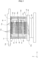
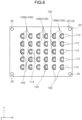
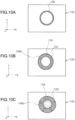
- FIG. 1 and FIG. 2 illustrate a probe card 90 as one embodiment of a "contact inspection device.”
- the probe card 90 includes a probe substrate 12 as a “circuit board”, a reinforcing plate 14, a probe head 16, and plural probes 100.
- the probe card 90 is electrically connected to a tester (not shown) and is attached to the tester for swingable motion relative to the tester.
- the probe substrate 12 has a disk-like shape, and is constituted as a multi-layer substrate including a ceramic substrate and a wiring substrate although not shown.
- Plural conductive contact portions 12a are provided on the -Z side surface as viewed in FIG. 1 (which is hereinafter referred to as "lower surface") of the probe substrate 12.
- the Z-axis in FIG. 1 indicates the "vertical direction,” and the "+Z side” and “-Z side” mean the "upside” and "downside,” respectively.
- each wiring path is electrically connected at one end to one of the probes 100 via one of the conductive contact portions 12a provided on the lower surface of the probe substrate 12, and it is connected at the other end to one of plural conductive portions (not shown) provided on the +Z side surface (which is hereinafter referred to as "upper surface") of the probe substrate 12.
- Each conductive portion (not shown) on the upper surface of the probe substrate 12 is connected to a tester (not shown).
- the reinforcing plate 14 is attached to the upper surface of the probe substrate 12.
- the reinforcing plate 14 has a disk-like shape and is formed with a metal member.
- the -Z side surface of the reinforcing plate 14, in other words, the lower surface of the reinforcing plate 14, which faces the upper surface of the probe substrate 12, is formed as a flat surface 14a.
- the flat surface 14a of the reinforcing plate 14 (refer to FIG. 1 ) is formed to have a predetermined flatness (for example, 30 pm) or better. Because the probe substrate 12 attached to the reinforcing plate 14 is forced to have the same flatness as the flat surface 14a, the reinforcing plate 14 defines the flatness of the probe substrate 12.
- the probe head 16 is detachably attached to the lower surface of the probe substrate 12 via fastening members 20.
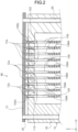
- the probe head 16 includes an upper probe head 22, a lower probe head 24, and an intermediate retaining member 26.
- the upper probe head 22 and the lower probe head 24 are spaced apart in the vertical direction.
- the upper probe head 22 is placed above and the lower probe head 24 is placed below in the vertical direction.
- the upper probe head 22 and the lower probe head 24 are formed of non-conductive material such as ceramic.
- the intermediate retaining member 26 is interposed between the upper probe head 22 and the lower probe head 24 in the vertical direction.
- the intermediate retaining member 26 is constituted as a film member made of non-conductive resin material.
- the upper probe head 22 has plural rotation restricting portions 102 (refer to FIG. 5 ), while the lower probe head 24 and the intermediate retaining member 26 have plural holes 24a and 26a respectively.
- the plural rotation restricting portion 102 and the plural holes 24a and 26a extend in the vertical direction, and have common axes extending in the vertical direction. In other words, each rotation restricting portion 102 and the holes 24a and 26a corresponding thereto are arranged coaxially.
- the rotation restricting portion 102 will be described in detail later.
- each probe 100 is inserted through a set of coaxially-arranged rotation restricting portion 102 and corresponding holes 24a and 26a.
- the probes 100 are inserted through the upper probe head 22, the lower probe head 24, and the intermediate retaining member 26.
- each probe 100 has a first end (lower end) 100a (refer to FIG. 3 ) and a second end (upper end) 100b (refer to FIG. 3 ) that individually protrude vertically from the probe head 16.
- the intermediate retaining member 26 In the state where the probes 100 are inserted through the rotation restricting portions 102 and the holes 24a and 26a, the intermediate retaining member 26 is forced to move in the direction intersecting the axial direction of the probes 100 (X-axis direction or Y-axis direction in FIG. 1 ). As a result, an intermediate portion 110 of each probe 100 is pressed by the intermediate retaining member 26 in the direction intersecting the axial direction such that mainly the intermediate portion 110 of the probe 100 bends in the direction intersecting the axial direction. In other words, the probes 100 bend in an arch-shape within the probe head 16, and the probes 100 are retained by the probe head 16.
- the plural probes 100 are bent and aligned in the direction intersecting the axial direction, that is, in the same direction, within the probe head 16, by the intermediate retaining member 26. Accordingly, the probe card 90, even when an overdrive acts on each probe 100 during inspection of the test object, is prevented from being short-circuited by the neighboring probes coming into contact each other in the bent state since the bending direction of the probes 100 are regulated in advance by the intermediate retaining member 26.
- an inspection stage 28 is provided below the probe card 90.
- the inspection stage 28 is constituted by combining an X-stage, a Y-stage, a Z-stage, and a ⁇ -stage.
- a chuck top 30 is mounted on top of the inspection stage 28.
- the chuck top 30 is positionally adjustable in an X-axis direction, a Y-axis direction orthogonal to the X-axis direction on a horizontal plane, and a vertical direction orthogonal to the horizontal plane (XY plane), i.e., a Z-axis direction.
- the chuck top 30 is also adjustable in its rotational position ( ⁇ -direction) about the Z-axis.
- a mounting surface 32, on which a test object 34 is mounted, is provided on top of the chuck top 30.
- the test object 34 is a semiconductor wafer into which multiple integrated circuits have been incorporated.
- Plural electrodes 34a are provided on an upper surface of the test object 34. Because the plural electrodes 34a are brought into contact with the first ends 100a of the probes 100 with the second ends 100b of the probes 100 being in contact with the contact portions 12a of the probe substrate 12, an electrical connection is established between the probe card 90 and the test object 34.
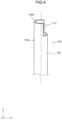
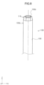
- Each probe 100 includes a first contact portion 104 forming the first end 100a of the probe 100 and an elastic portion 106.
- the elastic portion 106 is formed as a tubular member in this embodiment.
- the elastic portion 106 is provided with an extendable portion 108 having at least one spiral slit in the axial direction thereof.
- two extendable portions 108A and 108B are provided in the elastic portion 106.
- the intermediate portion 110 is provided between the extendable portions 108A and 108B.
- the first contact portion 104 is connected to a first end of the elastic portion 106. Specifically, the first contact portion 104 is welded to the first end of the elastic portion 106 ("lower end side" in FIG. 3 ).
- the elastic portion 106 has a welding part 106a at which the elastic portion 106 is welded to the first contact portion 104.
- the welding part 106a is larger in diameter than other parts of the elastic portion 106.
- the holes 24a and 26a of the probe head 16 have a diameter that is greater than that of the welding part 106a, i.e., the maximum diameter of the probes 100.
- extendable portions 108A and 108B are formed as spiral slits along the axial direction (vertical direction) of the elastic portion 106.
- the extendable portions 108A and 108B are capable of expanding and contracting along the axial direction of the elastic portion 106.
- the intermediate portion 110 which corresponds to the intermediate retaining member 26 when the probe 100 is inserted through the probe head 16, is provided between the extendable portions 108A and 108B.
- a contact point portion 106b and a rotation restricted portion 112 are provided on a second end of the elastic portion 106 ("upper end side" in FIG. 3 ).
- the contact point portion 106b is provided on the second end of the elastic portion 106, that is, on the second end 100b of the probe 100.
- a part of the elastic portion 106 on the side of the second end is cut away and is formed as a cutaway portion.
- the rotation restricted portion 112 is formed as the cutaway portion. It should be noted that while a cutaway amount of the cutaway portion in the radial direction of the elastic portion 106 is set to be smaller than the radius of the elastic portion 106 in this embodiment, the cutaway amount may also be set to a value larger than the radius of the elastic portion 106.
- the probes 100 are formed of conductive metal material.
- the probes 100 are formed of a conductive metal material having high toughness, such as nickel (Ni), nickel-phosphorus alloys (Ni-P), nickel-tungsten alloys (Ni-W), phosphor bronze, palladium-cobalt alloys (Pd-Co) and palladium-nickel-cobalt alloys (Pd-Ni-Co).
- the plural rotation restricting portions 102 in this embodiment are provided in the upper probe head 22 of the probe head 16. More specifically, the rotation restricting portions 102 are provided in the upper probe head 22 such that the rotation restricting portions 102 face the contact portions 12a of the probe substrate 12 with the probe head 16 being attached to the probe substrate 12.
- the rotation restricting portions 102 are formed in the shape of the second end of the probe 100, i.e., in the shape corresponding to the shape of the rotation restricted portions 112. More specifically, the rotation restricting portions 102 of this embodiment are formed in the shape of the second end of the probe 100, that is, a letter D-shape corresponding to the shape of the cutaway portion. Further, the rotation restricting portion 102 penetrates through the upper probe head 22.
- the rotation restricted portion 112 engages with the rotation restricting portion 102 of the probe head 16 to restrict the rotation of the probe 100 about the axial direction of the probe 100 in a state where the second end 100b of the probe 100, that is, the contact point portion 106b is in contact with the contact portion 12a of the probe substrate 12.
- generation of wear and damage of the contact portion between the contact point portion 106b and the contact portion 12a of the probe substrate 12 can be controlled.
- electrical connection between the probe 100 and the probe substrate 12 can be stabilized, and thus the reliability of the probe card 90 can be improved.
- the extendable portion 108 having a spiral slit provided between the first contact portion 104 and the contact point portion 106b contracts in the axial direction and absorbs a part of the pressing force. Then, although a part of the pressing force acts on the probe 100 to rotate the probe 100 about the axial direction, due to provision of the rotation restricted portion 112 that restricts the rotation of the probe 100 about the axial direction of the probe 100 on the second end 100b of the probe 100, the rotation of the probe at the second end 100b thereof about the axial direction is controlled.
- the elastic portion 106 of the probe 100 is formed of a tubular member. Therefore, when rotation occurs repeatedly between the contact point portion 106b of the elastic portion 106 of the probe 100 and the contact portion 12a of the probe substrate 12, the contact portion 12a of the probe substrate 12 wears out annularly. In other words, wear is concentrated on the same portion. As a result, fluctuation in contact pressure occurs between the probe 100 and the probe substrate 12, and electrical connection between the probe 100 and the probe substrate 12 becomes unstable.
- rotation of the contact point portion 106b about the axial direction of the probe 100 is restricted by the rotation restricted portion 112. Accordingly, the rotation at the contact point portion 106b is restricted even when the elastic portion 106 is formed by a tubular member. Thus, generation of wear and damage between the contact point portion 106b and the contact portion 12a of the probe substrate 12 can be controlled even more effectively, and electrical connection between the probe 100 and the probe substrate 12 can be stabilized.
- the rotation restricted portion 112 is formed as a cutaway portion, the rotation restricted portion 112 can be formed easily on the second end of the elastic portion 106.
- rotation restricted portions 116 and 118 are formed on the elastic portion 106 in a polygonal shape, force that acts on the rotation restricted portions 116 and 118 to restrict the rotation about the axial direction can be dispersed to each surface of the polygonal shape. Accordingly, less force is required to control the rotation of the second end 100b of the probe 100.
- an annular contact region 12b is formed when the contact point portion 106b rotates relative to the contact portion 12a of the probe substrate 12.
- an annular contact region 12c is formed when the contact point portion 106b rotates relative to the contact portion 12a of the probe substrate 12.
- This contact region 12c is a region formed between a circumscribed circle passing through vertices on an outer peripheral side of the hexagon and an inscribed circle passing through vertices on an inner peripheral side of the hexagon. Further, an area of the contact region 12c is larger than an area of the contact region 12b. As a result, frictional force between the contact portion 12a and the contact point portion 106b increases and this frictional force acts to prevent the rotation of the elastic portion 106. Thus, the rotation of the elastic portion 106 can be controlled. In addition, due to an increase in the contact area between the contact point portion 106b and the contact portion 12a, the contact pressure per unit area between the contact point portion 106b and the contact portion 12a can be reduced. Thus, wear of the contact portion 12a is reduced.
- FIG. 10(C) illustrates a case in which the shape of the rotation restricted portion 118 of the elastic portion 106 is formed as a star.
- a contact region 12d is a region formed between a circumscribed circle passing through vertices on an outer peripheral side of the star and an inscribed circle passing through vertices on an inner peripheral side of the star. With this configuration, an area of the contact region 12d is larger than that of the contact regions 12b and 12c. Thus, more of the above-described effect can be obtained by the contact region 12d than by the contact region 12c.
- the rotation restricted portions 116 and 118 on the second end of the elastic portion 106 into a polygonal shape, the contact area between the contact point portion 106b provided on the second end and the contact portion 12a of the probe substrate 12 increases, thereby increasing the frictional force between the contact point portion 106b and the contact portion 12a.
- the rotation of the probe 100 can be controlled.
- complex shapes can be easily formed on the second end of the elastic portion 106 (second end 100b of the probe 100).
- the strength (rigidity) of the tubular member can be increased.
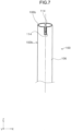
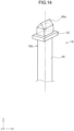
- a probe 68 according to the second embodiment includes a first contact portion 70 and an elastic portion 72.
- the elastic portion 72 is connected to the first contact portion 70 at an end on the -Z side in FIG. 11 .
- the elastic portion 72 has two extendable portions 74A and 74B with spiral slits (refer to FIG. 11 ) which are provided at an interval in the axial direction of the probe 68 (Z-axis direction in FIG. 11 ).
- an end of the elastic portion 72 on the +Z side in FIG. 11 shall be referred to as a contact point portion 76.
- An end of the elastic portion 72 with the contact point portion 76 is provided with the rotation restricted portion 78 (refer to FIG. 12 ).
- the rotation restricted portion 78 is formed as a protrusion that protrudes from the elastic portion 72 in the radial direction of the elastic portion 72.
- the rotation restricted portion 78 in this embodiment is formed in a rectangular shape.
- the rotation restricting portion 102 provided on the upper probe head 22 of the probe head 16 is formed as a rectangular through hole of a size corresponding to the rectangular rotation restricted portion 78. In other words, when the probe 68 is inserted through the probe head 16, the rotation restricted portion 78 of the probe 68 is in engagement with the rectangular rotation restricting portion 102 of the probe head 16. As a result, the rotation restricting portion 102 restricts the rotation of the rotation restricted portion 78, and thus the rotation of the probe 68 about the axial direction thereof is restricted.
- the probe card 10 of this embodiment is different from the first embodiment in that plural positioning members 36 and 38 are provided between the probe head 16 and the probe substrate 12 and that rotation restricting portions 56 and 58 are formed on the positioning members 36 and 38.
- plural holes 22a are formed in the upper probe head 22 of the probe head 16, instead of the rotation restricting portion 102.
- the plural holes 22a extend in the vertical direction (Z-axis), and have common axes extending in the vertical direction with the holes 24a and 26a.
- the axes of a set of holes 22a, 24a, and 26a are arranged coaxially.
- each probe 18 is inserted through a set of coaxially-arranged holes 22a, 24a, and 26a.
- the probes 18 are inserted through the upper probe head 22, the lower probe head 24, and the intermediate retaining member 26.
- each probe 18 has a first end 18a (refer to FIG. 13 ) and a second end 18b (refer to FIG. 13 ) that individually protrude vertically from the probe head 16.
- plural positioning members 36 and 38 are attached to an upper surface of the probe head 16, i.e., an upper surface of the upper probe head 22, via fastening members 40 and positioning pins 42.
- the positioning members 36 and 38 include a first positioning member 36 and a second positioning member 38.
- the positioning members 36 and 38 are described in detail later.
- the second ends 18b (refer to FIG. 13 ) of the probes 18 are inserted through the positioning members 36 and 38, and protrude toward the probe substrate 12 from the positioning members 36 and 38.
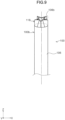
- Each probe 18 includes a first contact portion 44 forming the first end 18a of the probe 18, a second contact portion 46 forming the second end 18b of the probe 18, and an elastic portion 48.
- the first contact portion 44 and the second contact portion 46 are connected to opposite ends of the elastic portion 48.
- the first contact portion 44 and the second contact portion 46 are welded to opposite ends of the elastic portion 48.
- the elastic portion 48 has welding parts 48a and 48b at which the elastic portion 48 is welded to the first contact portion 44 and the second contact portion 46.
- the welding parts 48a and 48b are larger in diameter than other parts of the elastic portion 48.
- the holes 22a, 24a, and 26a of the probe head 16 have a diameter that is greater than that of the welding parts 48a and 48b, i.e., the maximum diameter of the probes 18.
- the elastic portion 48 is provided with extendable portions 50A and 50B (refer to FIG. 13 ) having spiral slits that generate an elastic force in the axial direction of the elastic portion 48 (in the vertical direction).
- the extendable portions 50A and 50B are provided at two locations spaced apart in the axial direction.
- An intermediate portion 48c which corresponds to the intermediate retaining member 26 when the probe 18 is inserted through the probe head 16, is provided between the extendable portions 50A and 50B.
- the second contact portion 46 has a polygonal rotation restricted portion 52. As shown in FIG. 14 , in this embodiment, the rotation restricted portion 52 has a rectangular shape. In this embodiment, the thickness of the rotation restricted portion 52 in the axial direction is at least larger than that of the first positioning member 36. In other words, the rotation restricted portion 52 has a sufficient thickness to engage the first positioning member 36 and the second positioning member 38 when the probe 18 is inserted through the first positioning member 36 and the second positioning member 38.
- the rotation restricted portion 52 has a size that is larger than the diameter of the holes 22a, 24a, and 26a of the probe head 16. In other words, when the probe 18 is inserted through the probe head 16, the rotation restricted portion 52 cannot pass through the hole 22a and the lower surface of the rotation restricted portion 52 abuts against the upper surface of the upper probe head 22. Thus, when the first contact portion 44 of the probe 18 is passed through its corresponding holes 22a, 24a, and 26a of the probe head 16 until it protrudes from the lower probe head 24, the rotation restricted portion 52 is supported by the upper probe head 22.
- the second contact portion 46 has a tip portion 46a having the shape of a triangular prism extending in a direction orthogonal to the axial direction (vertical direction), i.e., in the X-axis direction or Y-axis direction.
- One edge of the triangular prism extending in the axial direction thereof is located at the top of the tip portion 46a in the vertical direction, in other words, forms a ridge.
- the probes 18 are formed of conductive metal material similar to the probes 100.
- the first positioning member 36 and the second positioning member 38 are described.
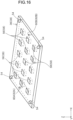
- the first positioning member 36 and the second positioning member 38 are formed as plate-like members made of non-conductive material such as ceramic. It should be noted that the first positioning member 36 is shown in FIG. 16 for descriptive purposes, and description is made using the first positioning member 36.
- the first positioning member 36 has through holes 54 (refer to FIG. 16 ), at its four corners, for fastening members 40 that are used to detachably attach the first positioning member 36 and the second positioning member 38 to the upper probe head 22.
- the through holes 54 are formed as slotted holes extending in a diagonal direction of the first positioning member 36 and the second positioning member 38. In FIG. 17 and FIG. 18 , illustration of the through holes 54 is omitted.
- the first positioning member 36 has plural rotation restricting portions 56 aligned at appropriate intervals in the X-axis direction and Y-axis direction.
- the rotation restricting portions 56 have a polygonal shape. In this embodiment, the rotation restricting portions 56 have a rectangular shape.
- the rotation restricting portions 56 have a size that is large enough that the rotation restricted portions 52 of the probes 18 can pass through them.
- the second positioning member 38 also has rotation restricting portions 58, which are similar to the rotation restricting portions 56 of the first positioning member 36.
- the first positioning member 36 has plural positioning holes 60A and 60B for receiving the positioning pins 42.
- the second positioning member 38 also has plural positioning holes 62A and 62B.
- the positioning holes 60A and 60B of the first positioning member 36 and the positioning holes 62A and 62B of the second positioning member 38 are formed such that the axes of the positioning holes 60A and 60B coincide with the axes of the positioning holes 62A and 62B when the first positioning member 36 and the second positioning member 38 are moved relative to each other, as described later.
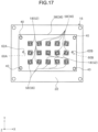
- the rectangular rotation restricting portions 56 of the first positioning member 36 and the rectangular restricting portions 58 of the second positioning member 38 are located at the same positions in the X-axis direction and Y-axis direction and overlap with each other at an upper part of the upper probe head 22. It should be noted that, in this state, the positioning holes 60A and 60B of the first positioning member 36 and the positioning holes 62A and 62B of the second positioning member 38 are offset from each other in the X-axis direction and Y- axis direction.
- FIG. 17 shows that the probes 18 are inserted from above the first positioning member 36 and the second positioning member 38 into the probe head 16 through the rotation restricting portions 56 and 58.
- FIG. 17 shows that the rotation restricted portions 52 of the probes 18 are received in the rotation restricting portions 56 and 58.
- the rotation restricted portions 52 are still unaligned, in other words, the ridges of the tip portions 46a of the second contact portions 46 are directed in different directions in the rotation restricting portions 56.
- the fastening members 40 are loosened.
- the first positioning member 36 and the second positioning member 38 are moved relative to each other on the upper probe head 22 without being removed therefrom. Specifically, the first positioning member 36 and the second positioning member 38 are moved along a diagonal of the rectangular rotation restricting portions 56 and 58.
- each of the first positioning member 36 and the second positioning member 38 engages two sets of two sides facing each other at rectangular rotation restricted portions 52, the rotation restricted portions 52 are restricted from moving in the X-axis direction and Y-axis direction. In other words, the rotation restricted portions 52 are positioned by the first positioning member 36 and the second positioning member 38. In addition, because the rotation restricting portions 56 and 58 engage the four sides of the rotation restricted portions 52, the rotation restricting portions 56 and 58 can restrict the rotation restricted portions 52 from rotating about the axes of the probes 18.
- the positioning pins 42 are inserted into the positioning hole 62A corresponding to the positioning hole 60A and into the positioning hole 62B corresponding to the positioning hole 60B, respectively.
- the positioning pins 42 are inserted into the positioning hole 62A corresponding to the positioning hole 60A and into the positioning hole 62B corresponding to the positioning hole 60B, respectively.
- the plural fastening members 40 by tightening the plural fastening members 40, relative positions of the first positioning member 36 and the second positioning member 38 can be fixed, and the position and rotation restricted state of each rotation restricted portion 52 can be maintained.
- the probes 18 can be switched from a rotation unrestricted state to a rotation restricted state.
- the first positioning member 36 and the second positioning member 38 can be moved relative to each other. Then, the probes 18 can be switched from the rotation restricted state to the rotation unrestricted state. Then, because the probes 18 can be individually pulled out from the probe head 16, any probes 18 damaged in the probe head 16 can be easily replaced.
- the probes 18 can be positioned and restricted from rotating simply by inserting the probes 18 into the probe head 16 and moving the first positioning member 36 and the second positioning member 38 relative to each other, the probe head 16 can be assembled easily.
- first positioning member 36 and the second positioning member 38 are provided at the upper part of the upper probe head 22 in this embodiment, only the first positioning member 36 may be provided at the upper part of the upper probe head 22.
- the size of the rotation restricting portion 56 of the first positioning member 36 a size corresponding to the rotation restricted portion 52 of the probe 18, the rotation of the probe 18 about the axial direction thereof can be restricted merely by receiving the rotation restricted portion 52 of the probe 18 by the rotation restricting portion 56.
Landscapes
- Physics & Mathematics (AREA)
- General Physics & Mathematics (AREA)
- Geometry (AREA)
- Engineering & Computer Science (AREA)
- Computer Hardware Design (AREA)
- Microelectronics & Electronic Packaging (AREA)
- General Engineering & Computer Science (AREA)
- Measuring Leads Or Probes (AREA)
- Testing Or Measuring Of Semiconductors Or The Like (AREA)
Claims (8)
- Sonde (100), die ein erstes Ende (100a) aufweist, das so konfiguriert ist, dass es mit einem Testobjekt (34) in Kontakt ist und davon trennt, und ein zweites Ende (100b), das so konfiguriert ist, dass es mit einer Leiterplatte (12) in Kontakt ist, um Inspektion des Testobjekts (34) durchzuführen, wobei das zweite Ende (100b) mit einem Abschnitt (52, 78, 112, 114, 116, 118) mit eingeschränkter Drehung bereitgestellt ist, der so konfiguriert ist, dass er Drehung einer Sonde (100) um die Axialrichtung davon einschränkt, dadurch gekennzeichnet ist, dassdas zweite Ende (100b) der Sonde (100) durch ein röhrenförmiges Element (106) gebildet ist,der Abschnitt (52, 78, 112, 114, 116, 118) mit eingeschränkter Drehung an einem Endabschnitt in einer Axialrichtung des röhrenförmigen Elements (106) bereitgestellt ist,ein ausstreckbarer Abschnitt (108), der in der Axialrichtung der Sonde (100) frei ausstreckbar und einziehbar ist und mindestens einen spiralförmigen Schlitz aufweist, zwischen dem ersten Ende (100a) und dem zweiten Ende (100b) bereitgestellt ist.
- Sonde (100) nach Anspruch 1, wobeider Abschnitt (52, 78, 112, 114, 116, 118) mit eingeschränkter Drehung so gebildet ist, dass er von einem durch das röhrenförmige Element (106) gebildeten Außenumfang nicht radial nach außen vorsteht, wo der Abschnitt (52, 78, 112, 114, 116, 118) mit eingeschränkter Drehung der Sonde (100) bereitgestellt ist, undder Abschnitt (52, 78, 112, 114, 116, 118) mit eingeschränkter Drehung als ein abgeschnittener Abschnitt gebildet ist, der durch Abschneiden eines Teils des röhrenförmigen Elements (106) des zweiten Endes (100b) gebildet ist.
- Sonde (100) nach Anspruch 1, wobeider Abschnitt (52, 78, 112, 114, 116, 118) mit eingeschränkter Drehung so gebildet ist, dass er von einem durch das röhrenförmige Element (106) gebildeten Außenumfang nicht radial nach außen vorsteht, wo der Abschnitt (52, 78, 112, 114, 116, 118) mit eingeschränkter Drehung der Sonde (100) bereitgestellt ist, undder Abschnitt (52, 78, 112, 114, 116, 118) mit eingeschränkter Drehung in einer polygonalen Form gebildet ist.
- Sonde (100) nach Anspruch 1, wobeider Abschnitt (52, 78, 112, 114, 116, 118) mit eingeschränkter Drehung als Vorsprung gebildet ist, der von einem durch das röhrenförmige Element (106) gebildeten Außenumfang radial nach außen vorsteht, wo der Abschnitt (52, 78, 112, 114, 116, 118) mit eingeschränkter Drehung der Sonde (100) bereitgestellt ist, undder Vorsprung eine polygonale Form aufweist.
- Sonde (100) nach Anspruch 1, wobeidas erste Ende (100a) durch einen ersten Kontaktabschnitt (44, 70, 104) gebildet ist,das zweite Ende (100b) durch einen zweiten Kontaktabschnitt (46) gebildet ist,wobei der erste Kontaktabschnitt (44, 70, 104) und der zweite Kontaktabschnitt (46) mit jedem Endabschnitt eines Zwischenabschnitts (48c, 110) verbunden sind, der durch das röhrenförmige Element (106) gebildet ist,der Abschnitt (52, 78, 112, 114, 116, 118) mit eingeschränkter Drehung als Vorsprung gebildet ist, der von einem Außenumfang des zweiten Kontaktabschnitts (46) radial nach außen vor vorsteht, undder Vorsprung in einer polygonalen Form mit einem größeren Durchmesser als der Zwischenabschnitt (48c, 110) gebildet ist.
- Sonde (100) nach einem der Ansprüche 1 bis 5, wobeimindestens zwei der ausstreckbaren Abschnitte (108A, 108B) zwischen dem ersten Ende (100a) und dem zweiten Ende (100b) bereitgestellt sind, undein Zwischenabschnitt (48c, 110) zwischen den ausstreckbaren Abschnitten (108A, 108B) gebildet ist.
- Sonde (100) nach Anspruch 5,
wobei der zweite Kontaktabschnitt (46) so konfiguriert ist, dass er einen Linienkontakt mit der Leiterplatte (12) herstellt. - Kontaktinspektionsvorrichtung, die so konfiguriert ist, dass sie Sondenkontaktinspektion eines Testobjekts (34) durchführt, umfassend:eine Leiterplatte (12), die so konfiguriert ist, dass sie mit einem zweiten Ende (100b) der Sonde (100) in Kontakt ist; undeinen Sondenkopf (16), durch den die mehreren Sonden (100) eingeführt werden und der abnehmbar an der Leiterplatte (12) befestigt ist, dadurch gekennzeichnet ist, dassdie Sonden (100) nach einem der Ansprüche 1 bis 7 sind, undeine Drehung einschränkender Abschnitt (56, 102), der in den Abschnitt (52, 78, 112, 114, 116, 118) mit eingeschränkter Drehung der Sonde (100) eingreift, an dem Sondenkopf (16) an einer Seite gegenüber der Leiterplatte (12) bereitgestellt ist.
Applications Claiming Priority (2)
| Application Number | Priority Date | Filing Date | Title |
|---|---|---|---|
| JP2014238713 | 2014-11-26 | ||
| JP2015148607A JP6484137B2 (ja) | 2014-11-26 | 2015-07-28 | プローブ及び接触検査装置 |
Publications (3)
| Publication Number | Publication Date |
|---|---|
| EP3026440A2 EP3026440A2 (de) | 2016-06-01 |
| EP3026440A3 EP3026440A3 (de) | 2016-06-08 |
| EP3026440B1 true EP3026440B1 (de) | 2024-08-21 |
Family
ID=54608393
Family Applications (1)
| Application Number | Title | Priority Date | Filing Date |
|---|---|---|---|
| EP15195356.9A Active EP3026440B1 (de) | 2014-11-26 | 2015-11-19 | Sonde und kontaktinspektionsvorrichtung |
Country Status (3)
| Country | Link |
|---|---|
| US (1) | US10024908B2 (de) |
| EP (1) | EP3026440B1 (de) |
| CN (1) | CN105628987B (de) |
Families Citing this family (14)
| Publication number | Priority date | Publication date | Assignee | Title |
|---|---|---|---|---|
| JP6221031B1 (ja) | 2016-12-16 | 2017-11-01 | 日本電産リード株式会社 | コンタクトプローブ及び電気接続治具 |
| JP7005939B2 (ja) * | 2017-05-25 | 2022-01-24 | 日本電産リード株式会社 | コンタクトプローブ |
| KR101860923B1 (ko) * | 2017-05-30 | 2018-05-24 | 황동원 | 반도체 디바이스 테스트용 콘택트 및 테스트 소켓장치 |
| USD847757S1 (en) * | 2017-08-30 | 2019-05-07 | Kabushiki Kaisha Nihon Micronics | Probe pin |
| CN109581006B (zh) * | 2017-09-29 | 2021-09-07 | 中华精测科技股份有限公司 | 探针装置及其矩形探针 |
| TWI748171B (zh) * | 2018-04-27 | 2021-12-01 | 日商日本電產理德股份有限公司 | 筒狀體及其製造方法 |
| US20200116755A1 (en) * | 2018-10-15 | 2020-04-16 | AIS Technology, Inc. | Test interface system and method of manufacture thereof |
| TWI857011B (zh) * | 2019-02-22 | 2024-10-01 | 日商日本電產理德股份有限公司 | 檢查治具 |
| TWI766154B (zh) * | 2019-03-27 | 2022-06-01 | 旺矽科技股份有限公司 | 探針頭及探針卡 |
| JP7620385B2 (ja) * | 2019-04-25 | 2025-01-23 | オムロン株式会社 | プローブピン、検査治具および検査ユニット |
| JP2021056158A (ja) * | 2019-10-01 | 2021-04-08 | 株式会社日本マイクロニクス | 電気的接触子、電気的接続構造及び電気的接続装置 |
| JP7566493B2 (ja) * | 2020-05-27 | 2024-10-15 | 株式会社日本マイクロニクス | 接続装置 |
| IT202000027149A1 (it) * | 2020-11-12 | 2022-05-12 | Technoprobe Spa | Testa di misura con un contatto migliorato tra sonde di contatto e fori guida metallizzati |
| TWI790065B (zh) * | 2021-12-27 | 2023-01-11 | 冠銓科技實業股份有限公司 | 應用高頻量測之測試針座結構改良 |
Citations (2)
| Publication number | Priority date | Publication date | Assignee | Title |
|---|---|---|---|---|
| US20020155735A1 (en) * | 2000-02-14 | 2002-10-24 | Yu Zhou | Contact structure and production method thereof and probe contact assembly using same |
| US20060191136A1 (en) * | 2002-07-24 | 2006-08-31 | Formfactor, Inc. | Method Of Making Microelectronic Spring Contact Array |
Family Cites Families (13)
| Publication number | Priority date | Publication date | Assignee | Title |
|---|---|---|---|---|
| US5521519A (en) * | 1992-07-30 | 1996-05-28 | International Business Machines Corporation | Spring probe with piloted and headed contact and method of tip formation |
| US7148709B2 (en) * | 2004-05-21 | 2006-12-12 | Microprobe, Inc. | Freely deflecting knee probe with controlled scrub motion |
| US8018242B2 (en) * | 2005-12-05 | 2011-09-13 | Nhk Spring Co., Ltd. | Probe card |
| JP2010281583A (ja) * | 2009-06-02 | 2010-12-16 | Nidec-Read Corp | 検査用治具 |
| JP5776687B2 (ja) * | 2010-04-19 | 2015-09-09 | 日本電産リード株式会社 | 検査用接触子及び検査用治具 |
| JP2011247838A (ja) * | 2010-05-31 | 2011-12-08 | Ricoh Co Ltd | スイッチプローブ、基板検査装置及び基板検査システム |
| CN103026242A (zh) * | 2010-07-29 | 2013-04-03 | 西川秀雄 | 检验夹具及触头 |
| JP2012042330A (ja) * | 2010-08-19 | 2012-03-01 | Micronics Japan Co Ltd | プローブカードの製造方法 |
| JP5487050B2 (ja) * | 2010-08-19 | 2014-05-07 | 株式会社日本マイクロニクス | プローブカードの製造方法 |
| JP5597108B2 (ja) * | 2010-11-29 | 2014-10-01 | 株式会社精研 | 接触検査用治具 |
| JP5944755B2 (ja) * | 2012-06-18 | 2016-07-05 | 株式会社日本マイクロニクス | 垂直動作式プローブカード |
| JP5947647B2 (ja) | 2012-07-25 | 2016-07-06 | 株式会社日本マイクロニクス | プローブカード、及び検査装置 |
| CN103852107A (zh) * | 2012-12-05 | 2014-06-11 | 上海清美绿色食品有限公司 | 生鲜食品物流用远程温湿传感系统 |
-
2015
- 2015-11-19 EP EP15195356.9A patent/EP3026440B1/de active Active
- 2015-11-19 US US14/945,655 patent/US10024908B2/en active Active
- 2015-11-26 CN CN201510836524.9A patent/CN105628987B/zh active Active
Patent Citations (2)
| Publication number | Priority date | Publication date | Assignee | Title |
|---|---|---|---|---|
| US20020155735A1 (en) * | 2000-02-14 | 2002-10-24 | Yu Zhou | Contact structure and production method thereof and probe contact assembly using same |
| US20060191136A1 (en) * | 2002-07-24 | 2006-08-31 | Formfactor, Inc. | Method Of Making Microelectronic Spring Contact Array |
Also Published As
| Publication number | Publication date |
|---|---|
| US10024908B2 (en) | 2018-07-17 |
| CN105628987A (zh) | 2016-06-01 |
| CN105628987B (zh) | 2019-05-17 |
| EP3026440A2 (de) | 2016-06-01 |
| EP3026440A3 (de) | 2016-06-08 |
| US20160146885A1 (en) | 2016-05-26 |
Similar Documents
| Publication | Publication Date | Title |
|---|---|---|
| EP3026440B1 (de) | Sonde und kontaktinspektionsvorrichtung | |
| EP3026439B1 (de) | Kontaktinspektionsvorrichtung | |
| EP3715866B1 (de) | Sondenkopf und sondenkarte | |
| JP6404008B2 (ja) | 電気的接触子及び電気的接続装置 | |
| US9535095B2 (en) | Anti-rotation for wire probes in a probe head of a die tester | |
| US8975908B2 (en) | Electrical test probe and probe assembly with improved probe tip | |
| KR20220116266A (ko) | 감소된 피치의 애플리케이션을 위한 프로브 헤드 | |
| JP2020504302A (ja) | 検査用プローブ及びソケット | |
| EP1243931A1 (de) | Prüfkopf mit vertikalen Prüfstiften für integrierte Halbleiterbausteine | |
| US10018653B2 (en) | Kelvin contact assembly in a testing apparatus for integrated circuits | |
| EP3605116A1 (de) | Vorrichtung für elektrische verbindung | |
| JP6484136B2 (ja) | 接触検査装置 | |
| US11029334B2 (en) | Low force wafer test probe | |
| EP3893005B1 (de) | Elektrische verbindungsvorrichtung und inspektionsverfahren | |
| US10571517B1 (en) | Probe head assembly | |
| US6407568B1 (en) | Apparatus for probing ends of pins | |
| TWI745750B (zh) | 電性連接件及電性連接裝置 | |
| US20180017596A1 (en) | Low force wafer test probe with variable geometry | |
| TWI879126B (zh) | 電性接觸子、電性連接構造及電性連接裝置 | |
| US20080088330A1 (en) | Nonconductive substrate with imbedded conductive pin(s) for contacting probe(s) | |
| JP2009145069A (ja) | プローブ装置 | |
| TWI671956B (zh) | 針腳插接元件以及具有該針腳插接元件之插座 | |
| KR20120086477A (ko) | 프로브카드용 니들탑재기판 |
Legal Events
| Date | Code | Title | Description |
|---|---|---|---|
| PUAL | Search report despatched |
Free format text: ORIGINAL CODE: 0009013 |
|
| PUAI | Public reference made under article 153(3) epc to a published international application that has entered the european phase |
Free format text: ORIGINAL CODE: 0009012 |
|
| AK | Designated contracting states |
Kind code of ref document: A2 Designated state(s): AL AT BE BG CH CY CZ DE DK EE ES FI FR GB GR HR HU IE IS IT LI LT LU LV MC MK MT NL NO PL PT RO RS SE SI SK SM TR |
|
| AX | Request for extension of the european patent |
Extension state: BA ME |
|
| AK | Designated contracting states |
Kind code of ref document: A3 Designated state(s): AL AT BE BG CH CY CZ DE DK EE ES FI FR GB GR HR HU IE IS IT LI LT LU LV MC MK MT NL NO PL PT RO RS SE SI SK SM TR |
|
| AX | Request for extension of the european patent |
Extension state: BA ME |
|
| RIC1 | Information provided on ipc code assigned before grant |
Ipc: G01R 1/073 20060101AFI20160429BHEP |
|
| 17P | Request for examination filed |
Effective date: 20161025 |
|
| RBV | Designated contracting states (corrected) |
Designated state(s): AL AT BE BG CH CY CZ DE DK EE ES FI FR GB GR HR HU IE IS IT LI LT LU LV MC MK MT NL NO PL PT RO RS SE SI SK SM TR |
|
| STAA | Information on the status of an ep patent application or granted ep patent |
Free format text: STATUS: EXAMINATION IS IN PROGRESS |
|
| 17Q | First examination report despatched |
Effective date: 20200406 |
|
| REG | Reference to a national code |
Ref country code: DE Ref legal event code: R079 Free format text: PREVIOUS MAIN CLASS: G01R0001073000 Ipc: G01R0001067000 Ref country code: DE Ref legal event code: R079 Ref document number: 602015089589 Country of ref document: DE Free format text: PREVIOUS MAIN CLASS: G01R0001073000 Ipc: G01R0001067000 |
|
| GRAP | Despatch of communication of intention to grant a patent |
Free format text: ORIGINAL CODE: EPIDOSNIGR1 |
|
| STAA | Information on the status of an ep patent application or granted ep patent |
Free format text: STATUS: GRANT OF PATENT IS INTENDED |
|
| RIC1 | Information provided on ipc code assigned before grant |
Ipc: G01R 1/073 20060101ALI20240305BHEP Ipc: G01R 1/067 20060101AFI20240305BHEP |
|
| INTG | Intention to grant announced |
Effective date: 20240322 |
|
| GRAS | Grant fee paid |
Free format text: ORIGINAL CODE: EPIDOSNIGR3 |
|
| GRAA | (expected) grant |
Free format text: ORIGINAL CODE: 0009210 |
|
| STAA | Information on the status of an ep patent application or granted ep patent |
Free format text: STATUS: THE PATENT HAS BEEN GRANTED |
|
| P01 | Opt-out of the competence of the unified patent court (upc) registered |
Free format text: CASE NUMBER: APP_40566/2024 Effective date: 20240709 |
|
| AK | Designated contracting states |
Kind code of ref document: B1 Designated state(s): AL AT BE BG CH CY CZ DE DK EE ES FI FR GB GR HR HU IE IS IT LI LT LU LV MC MK MT NL NO PL PT RO RS SE SI SK SM TR |
|
| REG | Reference to a national code |
Ref country code: GB Ref legal event code: FG4D |
|
| REG | Reference to a national code |
Ref country code: CH Ref legal event code: EP |
|
| REG | Reference to a national code |
Ref country code: IE Ref legal event code: FG4D |
|
| REG | Reference to a national code |
Ref country code: DE Ref legal event code: R096 Ref document number: 602015089589 Country of ref document: DE |
|
| REG | Reference to a national code |
Ref country code: LT Ref legal event code: MG9D |
|
| REG | Reference to a national code |
Ref country code: NL Ref legal event code: MP Effective date: 20240821 |
|
| PG25 | Lapsed in a contracting state [announced via postgrant information from national office to epo] |
Ref country code: NO Free format text: LAPSE BECAUSE OF FAILURE TO SUBMIT A TRANSLATION OF THE DESCRIPTION OR TO PAY THE FEE WITHIN THE PRESCRIBED TIME-LIMIT Effective date: 20241121 |
|
| REG | Reference to a national code |
Ref country code: AT Ref legal event code: MK05 Ref document number: 1715982 Country of ref document: AT Kind code of ref document: T Effective date: 20240821 |
|
| PG25 | Lapsed in a contracting state [announced via postgrant information from national office to epo] |
Ref country code: FI Free format text: LAPSE BECAUSE OF FAILURE TO SUBMIT A TRANSLATION OF THE DESCRIPTION OR TO PAY THE FEE WITHIN THE PRESCRIBED TIME-LIMIT Effective date: 20240821 Ref country code: NL Free format text: LAPSE BECAUSE OF FAILURE TO SUBMIT A TRANSLATION OF THE DESCRIPTION OR TO PAY THE FEE WITHIN THE PRESCRIBED TIME-LIMIT Effective date: 20240821 Ref country code: PT Free format text: LAPSE BECAUSE OF FAILURE TO SUBMIT A TRANSLATION OF THE DESCRIPTION OR TO PAY THE FEE WITHIN THE PRESCRIBED TIME-LIMIT Effective date: 20241223 Ref country code: PL Free format text: LAPSE BECAUSE OF FAILURE TO SUBMIT A TRANSLATION OF THE DESCRIPTION OR TO PAY THE FEE WITHIN THE PRESCRIBED TIME-LIMIT Effective date: 20240821 Ref country code: GR Free format text: LAPSE BECAUSE OF FAILURE TO SUBMIT A TRANSLATION OF THE DESCRIPTION OR TO PAY THE FEE WITHIN THE PRESCRIBED TIME-LIMIT Effective date: 20241122 |
|
| PG25 | Lapsed in a contracting state [announced via postgrant information from national office to epo] |
Ref country code: BG Free format text: LAPSE BECAUSE OF FAILURE TO SUBMIT A TRANSLATION OF THE DESCRIPTION OR TO PAY THE FEE WITHIN THE PRESCRIBED TIME-LIMIT Effective date: 20240821 |
|
| PG25 | Lapsed in a contracting state [announced via postgrant information from national office to epo] |
Ref country code: LV Free format text: LAPSE BECAUSE OF FAILURE TO SUBMIT A TRANSLATION OF THE DESCRIPTION OR TO PAY THE FEE WITHIN THE PRESCRIBED TIME-LIMIT Effective date: 20240821 |
|
| PG25 | Lapsed in a contracting state [announced via postgrant information from national office to epo] |
Ref country code: AT Free format text: LAPSE BECAUSE OF FAILURE TO SUBMIT A TRANSLATION OF THE DESCRIPTION OR TO PAY THE FEE WITHIN THE PRESCRIBED TIME-LIMIT Effective date: 20240821 Ref country code: IS Free format text: LAPSE BECAUSE OF FAILURE TO SUBMIT A TRANSLATION OF THE DESCRIPTION OR TO PAY THE FEE WITHIN THE PRESCRIBED TIME-LIMIT Effective date: 20241221 |
|
| PG25 | Lapsed in a contracting state [announced via postgrant information from national office to epo] |
Ref country code: HR Free format text: LAPSE BECAUSE OF FAILURE TO SUBMIT A TRANSLATION OF THE DESCRIPTION OR TO PAY THE FEE WITHIN THE PRESCRIBED TIME-LIMIT Effective date: 20240821 |
|
| PG25 | Lapsed in a contracting state [announced via postgrant information from national office to epo] |
Ref country code: RS Free format text: LAPSE BECAUSE OF FAILURE TO SUBMIT A TRANSLATION OF THE DESCRIPTION OR TO PAY THE FEE WITHIN THE PRESCRIBED TIME-LIMIT Effective date: 20241121 Ref country code: ES Free format text: LAPSE BECAUSE OF FAILURE TO SUBMIT A TRANSLATION OF THE DESCRIPTION OR TO PAY THE FEE WITHIN THE PRESCRIBED TIME-LIMIT Effective date: 20240821 |
|
| PG25 | Lapsed in a contracting state [announced via postgrant information from national office to epo] |
Ref country code: RS Free format text: LAPSE BECAUSE OF FAILURE TO SUBMIT A TRANSLATION OF THE DESCRIPTION OR TO PAY THE FEE WITHIN THE PRESCRIBED TIME-LIMIT Effective date: 20241121 Ref country code: PT Free format text: LAPSE BECAUSE OF FAILURE TO SUBMIT A TRANSLATION OF THE DESCRIPTION OR TO PAY THE FEE WITHIN THE PRESCRIBED TIME-LIMIT Effective date: 20241223 Ref country code: PL Free format text: LAPSE BECAUSE OF FAILURE TO SUBMIT A TRANSLATION OF THE DESCRIPTION OR TO PAY THE FEE WITHIN THE PRESCRIBED TIME-LIMIT Effective date: 20240821 Ref country code: NO Free format text: LAPSE BECAUSE OF FAILURE TO SUBMIT A TRANSLATION OF THE DESCRIPTION OR TO PAY THE FEE WITHIN THE PRESCRIBED TIME-LIMIT Effective date: 20241121 Ref country code: NL Free format text: LAPSE BECAUSE OF FAILURE TO SUBMIT A TRANSLATION OF THE DESCRIPTION OR TO PAY THE FEE WITHIN THE PRESCRIBED TIME-LIMIT Effective date: 20240821 Ref country code: LV Free format text: LAPSE BECAUSE OF FAILURE TO SUBMIT A TRANSLATION OF THE DESCRIPTION OR TO PAY THE FEE WITHIN THE PRESCRIBED TIME-LIMIT Effective date: 20240821 Ref country code: IS Free format text: LAPSE BECAUSE OF FAILURE TO SUBMIT A TRANSLATION OF THE DESCRIPTION OR TO PAY THE FEE WITHIN THE PRESCRIBED TIME-LIMIT Effective date: 20241221 Ref country code: HR Free format text: LAPSE BECAUSE OF FAILURE TO SUBMIT A TRANSLATION OF THE DESCRIPTION OR TO PAY THE FEE WITHIN THE PRESCRIBED TIME-LIMIT Effective date: 20240821 Ref country code: GR Free format text: LAPSE BECAUSE OF FAILURE TO SUBMIT A TRANSLATION OF THE DESCRIPTION OR TO PAY THE FEE WITHIN THE PRESCRIBED TIME-LIMIT Effective date: 20241122 Ref country code: FI Free format text: LAPSE BECAUSE OF FAILURE TO SUBMIT A TRANSLATION OF THE DESCRIPTION OR TO PAY THE FEE WITHIN THE PRESCRIBED TIME-LIMIT Effective date: 20240821 Ref country code: ES Free format text: LAPSE BECAUSE OF FAILURE TO SUBMIT A TRANSLATION OF THE DESCRIPTION OR TO PAY THE FEE WITHIN THE PRESCRIBED TIME-LIMIT Effective date: 20240821 Ref country code: BG Free format text: LAPSE BECAUSE OF FAILURE TO SUBMIT A TRANSLATION OF THE DESCRIPTION OR TO PAY THE FEE WITHIN THE PRESCRIBED TIME-LIMIT Effective date: 20240821 Ref country code: AT Free format text: LAPSE BECAUSE OF FAILURE TO SUBMIT A TRANSLATION OF THE DESCRIPTION OR TO PAY THE FEE WITHIN THE PRESCRIBED TIME-LIMIT Effective date: 20240821 |
|
| PG25 | Lapsed in a contracting state [announced via postgrant information from national office to epo] |
Ref country code: RO Free format text: LAPSE BECAUSE OF FAILURE TO SUBMIT A TRANSLATION OF THE DESCRIPTION OR TO PAY THE FEE WITHIN THE PRESCRIBED TIME-LIMIT Effective date: 20240821 Ref country code: DK Free format text: LAPSE BECAUSE OF FAILURE TO SUBMIT A TRANSLATION OF THE DESCRIPTION OR TO PAY THE FEE WITHIN THE PRESCRIBED TIME-LIMIT Effective date: 20240821 Ref country code: SM Free format text: LAPSE BECAUSE OF FAILURE TO SUBMIT A TRANSLATION OF THE DESCRIPTION OR TO PAY THE FEE WITHIN THE PRESCRIBED TIME-LIMIT Effective date: 20240821 |
|
| PG25 | Lapsed in a contracting state [announced via postgrant information from national office to epo] |
Ref country code: EE Free format text: LAPSE BECAUSE OF FAILURE TO SUBMIT A TRANSLATION OF THE DESCRIPTION OR TO PAY THE FEE WITHIN THE PRESCRIBED TIME-LIMIT Effective date: 20240821 |
|
| PG25 | Lapsed in a contracting state [announced via postgrant information from national office to epo] |
Ref country code: CZ Free format text: LAPSE BECAUSE OF FAILURE TO SUBMIT A TRANSLATION OF THE DESCRIPTION OR TO PAY THE FEE WITHIN THE PRESCRIBED TIME-LIMIT Effective date: 20240821 |
|
| PG25 | Lapsed in a contracting state [announced via postgrant information from national office to epo] |
Ref country code: SK Free format text: LAPSE BECAUSE OF FAILURE TO SUBMIT A TRANSLATION OF THE DESCRIPTION OR TO PAY THE FEE WITHIN THE PRESCRIBED TIME-LIMIT Effective date: 20240821 |
|
| REG | Reference to a national code |
Ref country code: DE Ref legal event code: R097 Ref document number: 602015089589 Country of ref document: DE |
|
| PLBE | No opposition filed within time limit |
Free format text: ORIGINAL CODE: 0009261 |
|
| STAA | Information on the status of an ep patent application or granted ep patent |
Free format text: STATUS: NO OPPOSITION FILED WITHIN TIME LIMIT |
|
| REG | Reference to a national code |
Ref country code: CH Ref legal event code: PL |
|
| PG25 | Lapsed in a contracting state [announced via postgrant information from national office to epo] |
Ref country code: MC Free format text: LAPSE BECAUSE OF FAILURE TO SUBMIT A TRANSLATION OF THE DESCRIPTION OR TO PAY THE FEE WITHIN THE PRESCRIBED TIME-LIMIT Effective date: 20240821 |
|
| PG25 | Lapsed in a contracting state [announced via postgrant information from national office to epo] |
Ref country code: LU Free format text: LAPSE BECAUSE OF NON-PAYMENT OF DUE FEES Effective date: 20241119 |
|
| REG | Reference to a national code |
Ref country code: CH Ref legal event code: PL |
|
| GBPC | Gb: european patent ceased through non-payment of renewal fee |
Effective date: 20241121 |
|
| PG25 | Lapsed in a contracting state [announced via postgrant information from national office to epo] |
Ref country code: CH Free format text: LAPSE BECAUSE OF NON-PAYMENT OF DUE FEES Effective date: 20241130 |
|
| 26N | No opposition filed |
Effective date: 20250522 |
|
| REG | Reference to a national code |
Ref country code: BE Ref legal event code: MM Effective date: 20241130 |
|
| PG25 | Lapsed in a contracting state [announced via postgrant information from national office to epo] |
Ref country code: SE Free format text: LAPSE BECAUSE OF FAILURE TO SUBMIT A TRANSLATION OF THE DESCRIPTION OR TO PAY THE FEE WITHIN THE PRESCRIBED TIME-LIMIT Effective date: 20240821 |
|
| PG25 | Lapsed in a contracting state [announced via postgrant information from national office to epo] |
Ref country code: BE Free format text: LAPSE BECAUSE OF NON-PAYMENT OF DUE FEES Effective date: 20241130 Ref country code: GB Free format text: LAPSE BECAUSE OF NON-PAYMENT OF DUE FEES Effective date: 20241121 |
|
| PG25 | Lapsed in a contracting state [announced via postgrant information from national office to epo] |
Ref country code: IE Free format text: LAPSE BECAUSE OF NON-PAYMENT OF DUE FEES Effective date: 20241119 |
|
| PGFP | Annual fee paid to national office [announced via postgrant information from national office to epo] |
Ref country code: DE Payment date: 20251119 Year of fee payment: 11 |
|
| PGFP | Annual fee paid to national office [announced via postgrant information from national office to epo] |
Ref country code: IT Payment date: 20251125 Year of fee payment: 11 |
|
| PGFP | Annual fee paid to national office [announced via postgrant information from national office to epo] |
Ref country code: FR Payment date: 20251125 Year of fee payment: 11 |