EP3015765B1 - High-power led lamp cooling device and manufacturing method therefor - Google Patents
High-power led lamp cooling device and manufacturing method therefor Download PDFInfo
- Publication number
- EP3015765B1 EP3015765B1 EP14818281.9A EP14818281A EP3015765B1 EP 3015765 B1 EP3015765 B1 EP 3015765B1 EP 14818281 A EP14818281 A EP 14818281A EP 3015765 B1 EP3015765 B1 EP 3015765B1
- Authority
- EP
- European Patent Office
- Prior art keywords
- type semiconductor
- semiconductor element
- column
- semiconductor elements
- led lamp
- Prior art date
- Legal status (The legal status is an assumption and is not a legal conclusion. Google has not performed a legal analysis and makes no representation as to the accuracy of the status listed.)
- Not-in-force
Links
Images
Classifications
-
- H—ELECTRICITY
- H10—SEMICONDUCTOR DEVICES; ELECTRIC SOLID-STATE DEVICES NOT OTHERWISE PROVIDED FOR
- H10H—INORGANIC LIGHT-EMITTING SEMICONDUCTOR DEVICES HAVING POTENTIAL BARRIERS
- H10H20/00—Individual inorganic light-emitting semiconductor devices having potential barriers, e.g. light-emitting diodes [LED]
- H10H20/80—Constructional details
- H10H20/85—Packages
- H10H20/858—Means for heat extraction or cooling
-
- F—MECHANICAL ENGINEERING; LIGHTING; HEATING; WEAPONS; BLASTING
- F21—LIGHTING
- F21V—FUNCTIONAL FEATURES OR DETAILS OF LIGHTING DEVICES OR SYSTEMS THEREOF; STRUCTURAL COMBINATIONS OF LIGHTING DEVICES WITH OTHER ARTICLES, NOT OTHERWISE PROVIDED FOR
- F21V29/00—Protecting lighting devices from thermal damage; Cooling or heating arrangements specially adapted for lighting devices or systems
- F21V29/50—Cooling arrangements
- F21V29/51—Cooling arrangements using condensation or evaporation of a fluid, e.g. heat pipes
-
- F—MECHANICAL ENGINEERING; LIGHTING; HEATING; WEAPONS; BLASTING
- F21—LIGHTING
- F21V—FUNCTIONAL FEATURES OR DETAILS OF LIGHTING DEVICES OR SYSTEMS THEREOF; STRUCTURAL COMBINATIONS OF LIGHTING DEVICES WITH OTHER ARTICLES, NOT OTHERWISE PROVIDED FOR
- F21V29/00—Protecting lighting devices from thermal damage; Cooling or heating arrangements specially adapted for lighting devices or systems
- F21V29/50—Cooling arrangements
- F21V29/51—Cooling arrangements using condensation or evaporation of a fluid, e.g. heat pipes
- F21V29/52—Cooling arrangements using condensation or evaporation of a fluid, e.g. heat pipes electrically powered, e.g. refrigeration systems
-
- F—MECHANICAL ENGINEERING; LIGHTING; HEATING; WEAPONS; BLASTING
- F21—LIGHTING
- F21V—FUNCTIONAL FEATURES OR DETAILS OF LIGHTING DEVICES OR SYSTEMS THEREOF; STRUCTURAL COMBINATIONS OF LIGHTING DEVICES WITH OTHER ARTICLES, NOT OTHERWISE PROVIDED FOR
- F21V29/00—Protecting lighting devices from thermal damage; Cooling or heating arrangements specially adapted for lighting devices or systems
- F21V29/50—Cooling arrangements
- F21V29/54—Cooling arrangements using thermoelectric means, e.g. Peltier elements
-
- F—MECHANICAL ENGINEERING; LIGHTING; HEATING; WEAPONS; BLASTING
- F21—LIGHTING
- F21V—FUNCTIONAL FEATURES OR DETAILS OF LIGHTING DEVICES OR SYSTEMS THEREOF; STRUCTURAL COMBINATIONS OF LIGHTING DEVICES WITH OTHER ARTICLES, NOT OTHERWISE PROVIDED FOR
- F21V29/00—Protecting lighting devices from thermal damage; Cooling or heating arrangements specially adapted for lighting devices or systems
- F21V29/50—Cooling arrangements
- F21V29/70—Cooling arrangements characterised by passive heat-dissipating elements, e.g. heat-sinks
-
- F—MECHANICAL ENGINEERING; LIGHTING; HEATING; WEAPONS; BLASTING
- F21—LIGHTING
- F21Y—INDEXING SCHEME ASSOCIATED WITH SUBCLASSES F21K, F21L, F21S and F21V, RELATING TO THE FORM OR THE KIND OF THE LIGHT SOURCES OR OF THE COLOUR OF THE LIGHT EMITTED
- F21Y2115/00—Light-generating elements of semiconductor light sources
- F21Y2115/10—Light-emitting diodes [LED]
-
- H—ELECTRICITY
- H10—SEMICONDUCTOR DEVICES; ELECTRIC SOLID-STATE DEVICES NOT OTHERWISE PROVIDED FOR
- H10H—INORGANIC LIGHT-EMITTING SEMICONDUCTOR DEVICES HAVING POTENTIAL BARRIERS
- H10H20/00—Individual inorganic light-emitting semiconductor devices having potential barriers, e.g. light-emitting diodes [LED]
- H10H20/01—Manufacture or treatment
- H10H20/036—Manufacture or treatment of packages
- H10H20/0365—Manufacture or treatment of packages of means for heat extraction or cooling
-
- H—ELECTRICITY
- H10—SEMICONDUCTOR DEVICES; ELECTRIC SOLID-STATE DEVICES NOT OTHERWISE PROVIDED FOR
- H10H—INORGANIC LIGHT-EMITTING SEMICONDUCTOR DEVICES HAVING POTENTIAL BARRIERS
- H10H20/00—Individual inorganic light-emitting semiconductor devices having potential barriers, e.g. light-emitting diodes [LED]
- H10H20/80—Constructional details
- H10H20/85—Packages
- H10H20/858—Means for heat extraction or cooling
- H10H20/8584—Means for heat extraction or cooling electrically controlled, e.g. Peltier elements
-
- H—ELECTRICITY
- H10—SEMICONDUCTOR DEVICES; ELECTRIC SOLID-STATE DEVICES NOT OTHERWISE PROVIDED FOR
- H10N—ELECTRIC SOLID-STATE DEVICES NOT OTHERWISE PROVIDED FOR
- H10N10/00—Thermoelectric devices comprising a junction of dissimilar materials, i.e. devices exhibiting Seebeck or Peltier effects
- H10N10/10—Thermoelectric devices comprising a junction of dissimilar materials, i.e. devices exhibiting Seebeck or Peltier effects operating with only the Peltier or Seebeck effects
- H10N10/13—Thermoelectric devices comprising a junction of dissimilar materials, i.e. devices exhibiting Seebeck or Peltier effects operating with only the Peltier or Seebeck effects characterised by the heat-exchanging means at the junction
-
- H—ELECTRICITY
- H10—SEMICONDUCTOR DEVICES; ELECTRIC SOLID-STATE DEVICES NOT OTHERWISE PROVIDED FOR
- H10W—GENERIC PACKAGES, INTERCONNECTIONS, CONNECTORS OR OTHER CONSTRUCTIONAL DETAILS OF DEVICES COVERED BY CLASS H10
- H10W40/00—Arrangements for thermal protection or thermal control
- H10W40/20—Arrangements for cooling
- H10W40/25—Arrangements for cooling characterised by their materials
-
- H—ELECTRICITY
- H10—SEMICONDUCTOR DEVICES; ELECTRIC SOLID-STATE DEVICES NOT OTHERWISE PROVIDED FOR
- H10W—GENERIC PACKAGES, INTERCONNECTIONS, CONNECTORS OR OTHER CONSTRUCTIONAL DETAILS OF DEVICES COVERED BY CLASS H10
- H10W40/00—Arrangements for thermal protection or thermal control
- H10W40/20—Arrangements for cooling
- H10W40/25—Arrangements for cooling characterised by their materials
- H10W40/251—Organics
Definitions
- the present invention relates to a high-power LED lamp cooling device and a method for manufacturing the same, which belongs to the field of heat-dissipating and cooling technology for a high-power LED lamp.
- the light-emitting efficiency of an LED lamp not only depends on quality of LED lamp bulb, but more importantly also depends on the temperature of the LED lamp during operation, especially when a high-power LED lamp is in operation, once the temperature is above 55°C, the light-emitting efficiency thereof reduces by about 2% for each degree increase in temperature, and therefore, cooling treatment is very important when an LED lamp, especially a high-power LED lamp is in operation.
- the high-power LED lamp is usually cooled by air cooling or with a semiconductor cooling device. The feature, that different temperatures are generated at a hot end and a cold end of a P-type semiconductor element and an N-type semiconductor element while being energized, has been widely applied in the field of manufacturing a semiconductor cooling or heating device.
- the N-type or P-type semiconductor elements are used to manufacture a cooling device, directions of the N-type or P-type semiconductor elements are always not taken into account, that is, when the N-type or P-type semiconductor elements are connected, the head end and the tail end of the N-type or P-type semiconductor elements are not distinguished, but arbitrary ends of the N-type or P-type semiconductor elements are connected mutually, such a mode of connection irrespective of the head end and the tail end not only reduces working efficiency of the semiconductor element, increases energy consumption, but also makes the manufactured cooling device fail to reach a required cooling temperature.
- the temperature difference between the hot end and the cold end thereof only can reach about 60 degrees.
- US 2010/127299 A1 discloses an actively cooled led lighting system and a method for making the same, where the lighting system can comprise one or more light emitting diodes (“LEDs”) that emit substantially white light and a thermoelectric cooler (“TEC”) for maintaining the LEDs within a temperature range (see Abstract).
- LEDs light emitting diodes
- TEC thermoelectric cooler
- an object of the present invention is to provide a high-power LED lamp cooling device and a method for manufacturing the same, which is featured by a better cooling effect, higher working efficiency and lower energy consumption.
- the present invention are implemented as follows: in the method for manufacturing a high-power LED lamp cooling device made of N-type semiconductor elements or P-type semiconductor elements, when the N-type semiconductor elements or the P-type semiconductor elements are used to manufacture the high-power LED lamp cooling device, manufacturing a semiconductor crystal bar used for manufacturing N-type semiconductor elements or P-type semiconductor elements in advance into a cone-shaped crystal bar of which one end has a large diameter and the other end has a small diameter, cutting the cone-shaped semiconductor crystal bar into slices to obtain wafers with the same thickness, the small-diameter end of the wafer being the head end the large-diameter end being the tail end, and then making a color mark on the tail end surface of each wafer; and then cutting and pelletizing the conical surface of each wafer to the same polygonal cylindrical shape, the polygonal cylindrical semiconductor is the N-type semiconductor elements or the P-type semiconductor elements with a head end and a tail end, arranging the N-type semiconductor elements and the P-type semiconductor elements in a matrix form between two
- the polygonal cylinder is a quadrangular, or square, or regular hexagonal, or regular octagonal, or regular decagonal or regular dodecagonal cylinder.
- a high-power LED lamp cooling device constructed according to the above method includes: N-type semiconductor elements and P-type semiconductor elements arranged in a matrix form between an upper beryllium-oxide ceramic wafer and a lower beryllium-oxide ceramic wafer which are provided with conductive circuits, an end of both the N-type semiconductor and the P-type semiconductor is provided with a conductive color mark, the end with the color mark is regarded as the tail end of the N-type semiconductor element or the P-type semiconductor element, the end without the color mark is regarded as the head end of the N-type semiconductor element or the P-type semiconductor element, each column of N-type semiconductor element and each column of P-type semiconductor element are connected in series respectively through an upper conductive plate provided on the upper beryllium-oxide ceramic wafer and through a lower conductive plate provided on the lower beryllium-oxide ceramic wafer, and the head end of each column of N-type semiconductor element is connected with the tail end of each column of P-type semiconductor element or the tail end of each column of N-
- a beryllium copper plate pressing block is attached on the upper surface of the upper beryllium-oxide ceramic wafer
- a heat dissipating aluminum base is mounted on the beryllium copper plate pressing block
- the bottom surface of the lower beryllium-oxide ceramic wafer is attached with a heat-conducting uniform temperature plate, through a graphene thermal conductive grease layer
- the heat-conducting uniform temperature plate is provided with a high-power LED lamp circuit which is mounted with an LED bulb, and both ends of the heat-conducting uniform temperature plate are connected to the aluminum base with screws, respectively
- the aluminum base is provided with a thermal pipe mounting hole for mounting a thermal conductive pipe of the heat sink.
- the heat-conducting uniform temperature plate is a printed circuit board for mounting a high power LED lamp circuit of an LED bulb.
- the semiconductor crystal bar is made with a color mark after being cut, so that the head end and tail end of the N-type semiconductor element or the P-type semiconductor element can be distinguished in a convenient way, and the arranging orientation of the head end or tail end is in consistent with that of the crystal bar before being cut.
- the semiconductor element in the present invention it is easy to distinguish the tail end and the head end, thus avoiding the occurrence of disordered connection when the N-type semiconductor element is connected in the prior art due to the undistinguishable head end and tail end.
- N-type or P-type semiconductor elements in the present invention are used to manufacture a cooling device, orderly connection in a head-to-tail sequence can be achieved in a convenient way, thereby effectively improving working efficiency of each N-type or P-type semiconductor element, as well as a cooling effect of the entire cooling device.
- the high-power LED lamp cooling device manufactured according to the present invention When the high-power LED lamp cooling device manufactured according to the present invention is adopted, the temperature difference between the cold end and the hot end thereof reaches about 73°C to 78°C, when the cooling device according to the present invention is mounted to a high-power LED lamp of 200W for use, it can be ensured that the circuit board of the high-power LED lamp can be stabilized under 45°C for a long time, thus effectively improving working efficiency of the high-power LED lamp and prolonging the service life of the high-power LED lamp.
- the present invention not only has a good cooling effect, a high working efficiency and a low energy consumption, but is also capable of reducing the light failure of a high power LED lamp, and prolonging the service life of the high-power LED lamp.
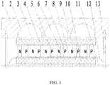
- FIG. 1 is a structural schematic diagram of the present invention.
- the embodiments are as follows: in the method for manufacturing a high-power LED lamp cooling device made of N-type semiconductor elements or P-type semiconductor elements, when the N-type semiconductor elements or the P-type semiconductor elements are used to manufacture the high-power LED lamp cooling device using a traditional process, manufacturing a semiconductor crystal bar used for manufacturing N-type semiconductor elements or P-type semiconductor elements into a cone-shaped crystal bar in advance, of which one end has a large diameter and the other end has a small diameter, cutting the cone-shaped semiconductor crystal bar into slices to obtain wafers with the same thickness, the small-diameter end of the wafer being the head end the large-diameter end being the tail end, and then making a color mark on the tail end surface of each wafer with colors made of conductive materials (for example, color materials made of conductive materials, such as copper, aluminium or silver); and then cutting and pelletizing the conical surface of each wafer to the same polygonal cylinder shape, the polygonal cylinder can be made as a quadrangular, square, regular hexagon
- the structural schematic diagram of the high-power LED lamp cooling device constructed according to the above method is as shown in FIG. 1 , and the cooling device includes: N-type semiconductor elements 6 and P-type semiconductor elements 7 arranged, in a matrix form, between an upper beryllium-oxide ceramic wafer 4 and a lower beryllium-oxide ceramic wafer 9 which are provided with conductive circuits, an end of both the N-type semiconductor 6 and the P-type semiconductor 7 is provided with a conductive color mark, the end with the color mark is regarded as the tail end of the N-type semiconductor element 6 or of the P-type semiconductor element 7, the end without the color mark is regarded as the head end of the N-type semiconductor element 6 or of the P-type semiconductor element 7, each column of N-type semiconductor element 6 and each column of P-type semiconductor element 7 are connected in series respectively through an upper conductive plate 5 provided on the upper beryllium-oxide ceramic wafer 4 and through a lower conductive plate 8 provided on the lower beryllium-oxide ceramic wafer 9, and the head
- a beryllium copper plate pressing block 3 is attached on the upper surface of the upper beryllium-oxide ceramic wafer 4, a heat dissipating aluminum base 1 is mounted on the beryllium copper plate pressing block 3, and meanwhile, the aluminum base 1 is manufactured with a thermal pipe mounting hole 2 for mounting a thermal conductive pipe of the heat sink; the bottom surface of the lower beryllium-oxide ceramic wafer 9 is attached with a heat-conducting uniform temperature plate 11, through a graphene thermal conductive grease layer 10, the heat-conducting uniform temperature plate 11 is manufactured with a high-power LED lamp circuit which is mounted with an LED bulb according to a traditional high-power LED lamp circuit, and the heat-conducting uniform temperature plate 11 also can directly adopt the existing printed circuit board for mounting a high power LED lamp circuit of an LED bulb; and finally both ends of the heat-conducting uniform temperature plate 11 are connected to the aluminum base 1 with screws 13, respectively.
- the high-power LED lamp cooling device When using the high-power LED lamp cooling device according to the present invention, it is only necessary to mount the device within a high-power LED lamp housing, mount the LED bulb on the heat-conducting uniform temperature plate 11, meanwhile clamp the thermal conductive pipe of the heat sink into the thermal pipe mounting hole 2 of the aluminum base 1, and connect power lines on the conductive wire 12 and the heat-conducting uniform temperature plate 11 respectively with the direct current power source.
Landscapes
- Engineering & Computer Science (AREA)
- General Engineering & Computer Science (AREA)
- Led Device Packages (AREA)
- Arrangement Of Elements, Cooling, Sealing, Or The Like Of Lighting Devices (AREA)
- Cooling Or The Like Of Semiconductors Or Solid State Devices (AREA)
Description
- The present invention relates to a high-power LED lamp cooling device and a method for manufacturing the same, which belongs to the field of heat-dissipating and cooling technology for a high-power LED lamp.
- The light-emitting efficiency of an LED lamp not only depends on quality of LED lamp bulb, but more importantly also depends on the temperature of the LED lamp during operation, especially when a high-power LED lamp is in operation, once the temperature is above 55°C, the light-emitting efficiency thereof reduces by about 2% for each degree increase in temperature, and therefore, cooling treatment is very important when an LED lamp, especially a high-power LED lamp is in operation. In the prior art, the high-power LED lamp is usually cooled by air cooling or with a semiconductor cooling device. The feature, that different temperatures are generated at a hot end and a cold end of a P-type semiconductor element and an N-type semiconductor element while being energized, has been widely applied in the field of manufacturing a semiconductor cooling or heating device. Currently, when the N-type or P-type semiconductor elements are used to manufacture a cooling device, directions of the N-type or P-type semiconductor elements are always not taken into account, that is, when the N-type or P-type semiconductor elements are connected, the head end and the tail end of the N-type or P-type semiconductor elements are not distinguished, but arbitrary ends of the N-type or P-type semiconductor elements are connected mutually, such a mode of connection irrespective of the head end and the tail end not only reduces working efficiency of the semiconductor element, increases energy consumption, but also makes the manufactured cooling device fail to reach a required cooling temperature. Generally speaking, in terms of the cooling device manufactured with the traditional method, the temperature difference between the hot end and the cold end thereof only can reach about 60 degrees. Accordingly, the effect of usage of the existing P-type semiconductor elements and N-type semiconductor elements for manufacturing a cooling device, especially a high-power LED lamp cooling device is less than desired.
US 2010/127299 A1 discloses an actively cooled led lighting system and a method for making the same, where the lighting system can comprise one or more light emitting diodes ("LEDs") that emit substantially white light and a thermoelectric cooler ("TEC") for maintaining the LEDs within a temperature range (see Abstract). - In order to overcome the defects in the prior art, an object of the present invention is to provide a high-power LED lamp cooling device and a method for manufacturing the same, which is featured by a better cooling effect, higher working efficiency and lower energy consumption.
- The present invention are implemented as follows: in the method for manufacturing a high-power LED lamp cooling device made of N-type semiconductor elements or P-type semiconductor elements, when the N-type semiconductor elements or the P-type semiconductor elements are used to manufacture the high-power LED lamp cooling device, manufacturing a semiconductor crystal bar used for manufacturing N-type semiconductor elements or P-type semiconductor elements in advance into a cone-shaped crystal bar of which one end has a large diameter and the other end has a small diameter, cutting the cone-shaped semiconductor crystal bar into slices to obtain wafers with the same thickness, the small-diameter end of the wafer being the head end the large-diameter end being the tail end, and then making a color mark on the tail end surface of each wafer; and then cutting and pelletizing the conical surface of each wafer to the same polygonal cylindrical shape, the polygonal cylindrical semiconductor is the N-type semiconductor elements or the P-type semiconductor elements with a head end and a tail end, arranging the N-type semiconductor elements and the P-type semiconductor elements in a matrix form between two beryllium-oxide ceramic chips which are provided with conductive circuits, and connecting each column of N-type semiconductor elements to the P-type semiconductor elements in series mutually, so that the head end of each column of N-type semiconductor elements in series is connected to the tail end of the P-type semiconductor elements or the tail end of each column of N-type semiconductor elements is connected to the head end of the P-type semiconductor elements.
- The polygonal cylinder is a quadrangular, or square, or regular hexagonal, or regular octagonal, or regular decagonal or regular dodecagonal cylinder.
- A high-power LED lamp cooling device constructed according to the above method, includes: N-type semiconductor elements and P-type semiconductor elements arranged in a matrix form between an upper beryllium-oxide ceramic wafer and a lower beryllium-oxide ceramic wafer which are provided with conductive circuits, an end of both the N-type semiconductor and the P-type semiconductor is provided with a conductive color mark, the end with the color mark is regarded as the tail end of the N-type semiconductor element or the P-type semiconductor element, the end without the color mark is regarded as the head end of the N-type semiconductor element or the P-type semiconductor element, each column of N-type semiconductor element and each column of P-type semiconductor element are connected in series respectively through an upper conductive plate provided on the upper beryllium-oxide ceramic wafer and through a lower conductive plate provided on the lower beryllium-oxide ceramic wafer, and the head end of each column of N-type semiconductor element is connected with the tail end of each column of P-type semiconductor element or the tail end of each column of N-type semiconductor element is connected with the head end of each column of P-type semiconductor element, each column of N-type semiconductor element and each column of P-type semiconductor element are connected with a direct current power source through a conductive wire on the upper conductive plate or the lower conductive plate provided at two outmost ends of the column. Where, a beryllium copper plate pressing block is attached on the upper surface of the upper beryllium-oxide ceramic wafer, a heat dissipating aluminum base is mounted on the beryllium copper plate pressing block, the bottom surface of the lower beryllium-oxide ceramic wafer is attached with a heat-conducting uniform temperature plate, through a graphene thermal conductive grease layer, the heat-conducting uniform temperature plate is provided with a high-power LED lamp circuit which is mounted with an LED bulb, and both ends of the heat-conducting uniform temperature plate are connected to the aluminum base with screws, respectively
- The aluminum base is provided with a thermal pipe mounting hole for mounting a thermal conductive pipe of the heat sink.
- The heat-conducting uniform temperature plate is a printed circuit board for mounting a high power LED lamp circuit of an LED bulb.
- Due to the above technical solution, based on the conventional manufacturing of N-type semiconductor element and P-type semiconductor element, the semiconductor crystal bar is made with a color mark after being cut, so that the head end and tail end of the N-type semiconductor element or the P-type semiconductor element can be distinguished in a convenient way, and the arranging orientation of the head end or tail end is in consistent with that of the crystal bar before being cut. In this way, when the semiconductor element in the present invention is used, it is easy to distinguish the tail end and the head end, thus avoiding the occurrence of disordered connection when the N-type semiconductor element is connected in the prior art due to the undistinguishable head end and tail end. When the N-type or P-type semiconductor elements in the present invention are used to manufacture a cooling device, orderly connection in a head-to-tail sequence can be achieved in a convenient way, thereby effectively improving working efficiency of each N-type or P-type semiconductor element, as well as a cooling effect of the entire cooling device. Through a test, when the high-power LED lamp cooling device manufactured according to the present invention is adopted, the temperature difference between the cold end and the hot end thereof reaches about 73°C to 78°C, when the cooling device according to the present invention is mounted to a high-power LED lamp of 200W for use, it can be ensured that the circuit board of the high-power LED lamp can be stabilized under 45°C for a long time, thus effectively improving working efficiency of the high-power LED lamp and prolonging the service life of the high-power LED lamp. Therefore, as compared with the prior art, the present invention not only has a good cooling effect, a high working efficiency and a low energy consumption, but is also capable of reducing the light failure of a high power LED lamp, and prolonging the service life of the high-power LED lamp.
-
FIG. 1 is a structural schematic diagram of the present invention. - Reference signs: 1-Aluminum base, 2-Thermal pipe mounting hole, 3-Beryllium copper plate pressing block, 4-Upper beryllium-oxide ceramic wafer, 5-Upper conductive plate, 6-N-type semiconductor element, 7-P-type semiconductor element, 8-Lower conductive plate, 9-Lower beryllium-oxide ceramic wafer, 10-Graphene thermal conductive grease layer, 11-Heat-conducting uniform temperature plate , 12-Conductive wire, 13-Screw.
- The present invention is described below in further detail with reference to accompanying drawings and the embodiments.
- The embodiments are as follows: in the method for manufacturing a high-power LED lamp cooling device made of N-type semiconductor elements or P-type semiconductor elements, when the N-type semiconductor elements or the P-type semiconductor elements are used to manufacture the high-power LED lamp cooling device using a traditional process, manufacturing a semiconductor crystal bar used for manufacturing N-type semiconductor elements or P-type semiconductor elements into a cone-shaped crystal bar in advance, of which one end has a large diameter and the other end has a small diameter, cutting the cone-shaped semiconductor crystal bar into slices to obtain wafers with the same thickness, the small-diameter end of the wafer being the head end the large-diameter end being the tail end, and then making a color mark on the tail end surface of each wafer with colors made of conductive materials (for example, color materials made of conductive materials, such as copper, aluminium or silver); and then cutting and pelletizing the conical surface of each wafer to the same polygonal cylinder shape, the polygonal cylinder can be made as a quadrangular, square, regular hexagonal, regular octagonal, regular decagonal or regular dodecagonal cylinder according to needs of use, the manufactured semiconductor with polygonal cylinder shape is the N-type semiconductor elements or the P-type semiconductor elements with a head end and a tail end; arranging the N-type semiconductor elements and the P-type semiconductor elements in a traditional matrix form between two beryllium-oxide ceramic chips which are provided with conductive circuits, and connecting each column of N-type semiconductor elements to the P-type semiconductor elements in series mutually, so that the head end of each column of N-type semiconductor elements in series can be connected to the tail end of the P-type semiconductor elements or the tail end of each column of N-type semiconductor elements can be connected to the head end of the P-type semiconductor elements.
- The structural schematic diagram of the high-power LED lamp cooling device constructed according to the above method is as shown in
FIG. 1 , and the cooling device includes: N-type semiconductor elements 6 and P-type semiconductor elements 7 arranged, in a matrix form, between an upper beryllium-oxideceramic wafer 4 and a lower beryllium-oxideceramic wafer 9 which are provided with conductive circuits, an end of both the N-type semiconductor 6 and the P-type semiconductor 7 is provided with a conductive color mark, the end with the color mark is regarded as the tail end of the N-type semiconductor element 6 or of the P-type semiconductor element 7, the end without the color mark is regarded as the head end of the N-type semiconductor element 6 or of the P-type semiconductor element 7, each column of N-type semiconductor element 6 and each column of P-type semiconductor element 7 are connected in series respectively through an upperconductive plate 5 provided on the upper beryllium-oxideceramic wafer 4 and through a lowerconductive plate 8 provided on the lower beryllium-oxideceramic wafer 9, and the head end of each column of N-type semiconductor element 6 is connected with the tail end of each column of P-type semiconductor element 7 or the tail end of each column of N-type semiconductor element 6 is connected with the head end of each column of P-type semiconductor element 7, each column of N-type semiconductor element 6 and each column of P-type semiconductor element 7 are connected with the direct current power source through aconductive wire 12 on the upperconductive plate 5 or the lowerconductive plate 8 provided at two outmost ends of the column (as shown inFIG. 1 ); during manufacturing, a beryllium copperplate pressing block 3 is attached on the upper surface of the upper beryllium-oxideceramic wafer 4, a heat dissipatingaluminum base 1 is mounted on the beryllium copperplate pressing block 3, and meanwhile, thealuminum base 1 is manufactured with a thermalpipe mounting hole 2 for mounting a thermal conductive pipe of the heat sink; the bottom surface of the lower beryllium-oxideceramic wafer 9 is attached with a heat-conductinguniform temperature plate 11, through a graphene thermalconductive grease layer 10, the heat-conductinguniform temperature plate 11 is manufactured with a high-power LED lamp circuit which is mounted with an LED bulb according to a traditional high-power LED lamp circuit, and the heat-conductinguniform temperature plate 11 also can directly adopt the existing printed circuit board for mounting a high power LED lamp circuit of an LED bulb; and finally both ends of the heat-conductinguniform temperature plate 11 are connected to thealuminum base 1 withscrews 13, respectively. - When using the high-power LED lamp cooling device according to the present invention, it is only necessary to mount the device within a high-power LED lamp housing, mount the LED bulb on the heat-conducting
uniform temperature plate 11, meanwhile clamp the thermal conductive pipe of the heat sink into the thermalpipe mounting hole 2 of thealuminum base 1, and connect power lines on theconductive wire 12 and the heat-conductinguniform temperature plate 11 respectively with the direct current power source.
Claims (5)
- A method for manufacturing a high-power LED lamp cooling device, comprising using an N-type semiconductor element and a P-type semiconductor element as a cooling component of the high-power LED lamp cooling device, and comprising: when the N-type semiconductor element and the P-type semiconductor element are used as cooling component of the high-power LED lamp cooling device, manufacturing a semiconductor crystal bar used for manufacturing the N-type semiconductor elements or the P-type semiconductor elements in advance into a cone-shaped crystal bar, of which one end has a large diameter and the other end has a small diameter, cutting the cone-shaped semiconductor crystal bar into slices to obtain wafers with the same thickness, the small-diameter end of the wafer being the head end and the large-diameter end being the tail end, and then making a color mark on the tail end surface of each wafer; and then cutting and pelletizing the conical surface of each wafer to the same polygonal cylindrical shape, the polygonal cylindrical semiconductor is the N-type semiconductor elements or the P-type semiconductor elements with a head end and a tail end, arranging the N-type semiconductor elements and the P-type semiconductor elements in a matrix form between two beryllium-oxide ceramic chips which are provided with conductive circuits, and connecting each column of N-type semiconductor elements to the P-type semiconductor elements in series mutually, so that the head end of each column of N-type semiconductor elements in series is connected to the tail end of the P-type semiconductor elements or the tail end of each column of N-type semiconductor elements is connected to the head end of the P-type semiconductor elements.
- The method for manufacturing a high-power LED lamp cooling device according to claim 1, wherein, the polygonal cylinder is a quadrangular, or square, or regular hexagonal, or regular octagonal, or regular decagonal or regular dodecagonal cylinder.
- A high-power LED lamp cooling device, comprising: N-type semiconductor elements (6) and P-type semiconductor elements (7) arranged in a matrix form between an upper beryllium-oxide ceramic wafer (4) and a lower beryllium-oxide ceramic wafer (9) which are provided with conductive circuits, wherein, an end of both the N-type semiconductor (6) and the P-type semiconductor (7) is provided with a conductive color mark, the end with the color mark is regarded as the tail end of the N-type semiconductor element (6) or the P-type semiconductor element (7), the end without the color mark is regarded as the head end of the N-type semiconductor element (6) or the P-type semiconductor element (7), each column of N-type semiconductor element (6) and each column of P-type semiconductor element (7) are connected in series respectively through an upper conductive plate (5) provided on the upper beryllium-oxide ceramic wafer (4) and through a lower conductive plate (8) provided on the lower beryllium-oxide ceramic wafer (9), and the head end of each column of N-type semiconductor element (6) is connected with the tail end of each column of P-type semiconductor element (7) or the tail end of each column of N-type semiconductor element (6) is connected with the head end of each column of P-type semiconductor element (7), each column of N-type semiconductor element (6) and each column of P-type semiconductor element (7) are connected with a direct current power source through a conductive wire (12) on the upper conductive plate (5) or the lower conductive plate (8) provided at two outmost ends of the column;
wherein, a beryllium copper plate pressing block (3) is attached on an upper surface of the upper beryllium-oxide ceramic wafer (4), a heat dissipating aluminum base (1) is mounted on the beryllium copper plate pressing block (3), a bottom surface of the lower beryllium-oxide ceramic wafer (9) is attached with a heat-conducting uniform temperature plate (11), through a graphene thermal conductive grease layer (10), the heat-conducting uniform temperature plate (11) is provided with a high-power LED lamp circuit which is mounted with an LED bulb, and both ends of the heat-conducting uniform temperature plate (11) are connected to the aluminum base (1) with screws (13), respectively. - The high-power LED lamp cooling device according to claim 3, wherein, the aluminum base (1) is manufactured with a thermal pipe mounting hole (2) for mounting a thermal conductive pipe of a heat sink.
- The high-power LED lamp cooling device according to claim 3, wherein, the heat-conducting uniform temperature plate (11) is a printed circuit board for mounting a high power LED lamp circuit of an LED bulb.
Applications Claiming Priority (2)
| Application Number | Priority Date | Filing Date | Title |
|---|---|---|---|
| CN201310257924.5A CN103353098B (en) | 2013-06-25 | 2013-06-25 | A kind of high-powered LED lamp cooling device and preparation method thereof |
| PCT/CN2014/078443 WO2014206166A1 (en) | 2013-06-25 | 2014-05-26 | High-power led lamp cooling device and manufacturing method therefor |
Publications (3)
| Publication Number | Publication Date |
|---|---|
| EP3015765A1 EP3015765A1 (en) | 2016-05-04 |
| EP3015765A4 EP3015765A4 (en) | 2016-06-29 |
| EP3015765B1 true EP3015765B1 (en) | 2018-08-08 |
Family
ID=49309494
Family Applications (1)
| Application Number | Title | Priority Date | Filing Date |
|---|---|---|---|
| EP14818281.9A Not-in-force EP3015765B1 (en) | 2013-06-25 | 2014-05-26 | High-power led lamp cooling device and manufacturing method therefor |
Country Status (7)
| Country | Link |
|---|---|
| US (1) | US9412925B2 (en) |
| EP (1) | EP3015765B1 (en) |
| JP (1) | JP6151449B2 (en) |
| CN (1) | CN103353098B (en) |
| AU (1) | AU2014301912B2 (en) |
| DK (1) | DK3015765T3 (en) |
| WO (1) | WO2014206166A1 (en) |
Families Citing this family (8)
| Publication number | Priority date | Publication date | Assignee | Title |
|---|---|---|---|---|
| CN103353098B (en) * | 2013-06-25 | 2015-09-23 | 陈志明 | A kind of high-powered LED lamp cooling device and preparation method thereof |
| CN103779288A (en) * | 2014-01-18 | 2014-05-07 | 西安交通大学 | Serial-parallel coupler-in-emulsion semiconductor refrigeration module based on double power supplies |
| CN105376971A (en) * | 2015-10-08 | 2016-03-02 | 京东方科技集团股份有限公司 | A shell of a mobile electronic apparatus and a mobile electronic apparatus |
| CN105202800A (en) * | 2015-10-24 | 2015-12-30 | 唐玉敏 | Semiconductor cooling and heating chip |
| JP7151068B2 (en) * | 2016-12-26 | 2022-10-12 | 三菱マテリアル株式会社 | Thermoelectric conversion module with case |
| US11616185B2 (en) * | 2017-06-01 | 2023-03-28 | Qualcomm Incorporated | Energy harvesting device for electronic devices |
| US20190178486A1 (en) * | 2017-12-13 | 2019-06-13 | Wei Chen | Module for led lighting fixture |
| CN111726934B (en) * | 2020-07-02 | 2022-11-11 | 西安电子科技大学芜湖研究院 | Heat dissipation drive plate utilizing semiconductor for cooling |
Family Cites Families (29)
| Publication number | Priority date | Publication date | Assignee | Title |
|---|---|---|---|---|
| JPH0770856B2 (en) * | 1989-02-27 | 1995-07-31 | 太陽誘電株式会社 | Position detection method for hybrid integrated circuit board |
| US5209786A (en) * | 1990-10-09 | 1993-05-11 | Thermo Electron Technologies Corporation | Integrity-enhanced thermoelectrics |
| JP3465879B2 (en) * | 1999-02-23 | 2003-11-10 | オリオン機械株式会社 | Manufacturing method of thermoelectric conversion module |
| JP2002076451A (en) * | 2000-09-04 | 2002-03-15 | Eco Twenty One:Kk | Manufacturing method of thermoelectric conversion element and thermoelectric conversion element |
| JP2004335499A (en) * | 2003-04-30 | 2004-11-25 | Yamaha Corp | Thermoelectric material and its manufacturing method |
| CN100397671C (en) * | 2003-10-29 | 2008-06-25 | 京瓷株式会社 | Thermoelectric conversion module |
| EP2572932B1 (en) * | 2003-12-11 | 2015-04-22 | Philips Solid-State Lighting Solutions, Inc. | Thermal management for lighting devices |
| JP4385891B2 (en) * | 2004-08-18 | 2009-12-16 | ソニー株式会社 | Display device |
| JP2007066696A (en) * | 2005-08-31 | 2007-03-15 | Matsushita Electric Ind Co Ltd | Lighting device |
| US8143769B2 (en) * | 2008-09-08 | 2012-03-27 | Intematix Corporation | Light emitting diode (LED) lighting device |
| US20100127299A1 (en) * | 2008-11-25 | 2010-05-27 | Cooper Technologies Company | Actively Cooled LED Lighting System and Method for Making the Same |
| US8809820B2 (en) * | 2010-01-27 | 2014-08-19 | Heraeus Noblelight Fusion Uv Inc. | Micro-channel-cooled high heat load light emitting device |
| US8931933B2 (en) * | 2010-03-03 | 2015-01-13 | Cree, Inc. | LED lamp with active cooling element |
| KR101055095B1 (en) * | 2010-03-09 | 2011-08-08 | 엘지이노텍 주식회사 | Light emitting device |
| US8807799B2 (en) * | 2010-06-11 | 2014-08-19 | Intematix Corporation | LED-based lamps |
| KR101822600B1 (en) * | 2010-07-29 | 2018-01-26 | 엘지이노텍 주식회사 | Led lighting apparatus comprising led module embedded thermoelectric cooling module |
| CN201819471U (en) * | 2010-10-15 | 2011-05-04 | 常山县万谷电子科技有限公司 | High power refrigeration piece |
| US9068701B2 (en) * | 2012-01-26 | 2015-06-30 | Cree, Inc. | Lamp structure with remote LED light source |
| US9234655B2 (en) * | 2011-02-07 | 2016-01-12 | Cree, Inc. | Lamp with remote LED light source and heat dissipating elements |
| US9103540B2 (en) * | 2011-04-21 | 2015-08-11 | Optalite Technologies, Inc. | High efficiency LED lighting system with thermal diffusion |
| CN102297544A (en) * | 2011-08-26 | 2011-12-28 | 陈志明 | Semiconductor refrigerating or heating module and production method thereof |
| US20130088848A1 (en) * | 2011-10-06 | 2013-04-11 | Intematix Corporation | Solid-state lamps with improved radial emission and thermal performance |
| US8992051B2 (en) * | 2011-10-06 | 2015-03-31 | Intematix Corporation | Solid-state lamps with improved radial emission and thermal performance |
| CN202521346U (en) * | 2012-04-24 | 2012-11-07 | 山西吉天利半导体照明有限公司 | Light emitting diode (LED) light source module cooled by adopting semiconductor cooler |
| CN102810620A (en) * | 2012-07-13 | 2012-12-05 | 重庆绿色科技开发有限公司 | Light emitting diode (LED) encapsulated by adopting semiconductor refrigeration plate as support |
| CN103398358B (en) * | 2013-06-25 | 2015-10-21 | 陈志明 | A kind of low light attenuation high-power LED street lamp and preparation method thereof |
| CN103353098B (en) * | 2013-06-25 | 2015-09-23 | 陈志明 | A kind of high-powered LED lamp cooling device and preparation method thereof |
| CN203336367U (en) * | 2013-06-25 | 2013-12-11 | 陈志明 | Low-light-failure and high-power LED street lamp |
| CN203336546U (en) * | 2013-06-25 | 2013-12-11 | 陈志明 | High-power LED lamp cooling device |
-
2013
- 2013-06-25 CN CN201310257924.5A patent/CN103353098B/en not_active Expired - Fee Related
-
2014
- 2014-05-26 AU AU2014301912A patent/AU2014301912B2/en not_active Ceased
- 2014-05-26 EP EP14818281.9A patent/EP3015765B1/en not_active Not-in-force
- 2014-05-26 WO PCT/CN2014/078443 patent/WO2014206166A1/en not_active Ceased
- 2014-05-26 DK DK14818281.9T patent/DK3015765T3/en active
- 2014-05-26 JP JP2016522205A patent/JP6151449B2/en not_active Expired - Fee Related
-
2015
- 2015-12-24 US US14/998,284 patent/US9412925B2/en not_active Expired - Fee Related
Non-Patent Citations (1)
| Title |
|---|
| None * |
Also Published As
| Publication number | Publication date |
|---|---|
| JP6151449B2 (en) | 2017-06-21 |
| CN103353098A (en) | 2013-10-16 |
| WO2014206166A1 (en) | 2014-12-31 |
| AU2014301912A1 (en) | 2016-02-11 |
| EP3015765A4 (en) | 2016-06-29 |
| CN103353098B (en) | 2015-09-23 |
| EP3015765A1 (en) | 2016-05-04 |
| US20160133811A1 (en) | 2016-05-12 |
| AU2014301912B2 (en) | 2017-10-19 |
| US9412925B2 (en) | 2016-08-09 |
| JP2016530674A (en) | 2016-09-29 |
| DK3015765T3 (en) | 2018-11-26 |
Similar Documents
| Publication | Publication Date | Title |
|---|---|---|
| US9412925B2 (en) | High-power LED lamp cooling device and method for manufacturing the same | |
| EP3015764B1 (en) | Low-light-failure high-power led road lamp and manufacturing method therefor | |
| CN201110527Y (en) | A high-power LED light source | |
| CN106678563A (en) | Photo-thermal integration type LED lighting lamp and manufacturing method thereof | |
| Cheng | Thermal management of high-power white LED package | |
| CN203336367U (en) | Low-light-failure and high-power LED street lamp | |
| CN102878455A (en) | Intelligent semiconductor heat radiating LED (light-emitting diode) lamp | |
| CN103050607B (en) | LED heat radiation substrate | |
| CN202024135U (en) | High-efficiency LED bulbs | |
| CN203336546U (en) | High-power LED lamp cooling device | |
| CN201331035Y (en) | High-power luminous LED illumination device based on semiconductor refrigeration heat radiation | |
| CN201462470U (en) | Semiconductor light-emitting diode floodlight with radiator | |
| CN201547725U (en) | A cooling device for an LED lamp | |
| CN206582553U (en) | A kind of light-heat integration LED illumination lamp | |
| CN203297992U (en) | LED bulb lamp emitting light by 360 degrees | |
| CN203258459U (en) | LED single-board ceramic lamp | |
| CN203810340U (en) | LED (light-emitting diode) high bay light with plurality of radiators | |
| CN201285012Y (en) | LED light projector | |
| CN204114879U (en) | LED module and LED light device | |
| CN201628123U (en) | A LED energy-saving light bulb | |
| CN100520153C (en) | Method for producing light-alltenuation proof high-power semiconductor lighting lamp | |
| CN206236665U (en) | A kind of great power LED heat sink structure | |
| CN103939772A (en) | LED photoelectricity-heat integrated module lamp | |
| CN203147707U (en) | Ceramic heat radiator for LED lamp | |
| CN203812918U (en) | Concave-type all-metal composite substrate in flip package main heat-dissipation channel |
Legal Events
| Date | Code | Title | Description |
|---|---|---|---|
| PUAI | Public reference made under article 153(3) epc to a published international application that has entered the european phase |
Free format text: ORIGINAL CODE: 0009012 |
|
| 17P | Request for examination filed |
Effective date: 20160122 |
|
| AK | Designated contracting states |
Kind code of ref document: A1 Designated state(s): AL AT BE BG CH CY CZ DE DK EE ES FI FR GB GR HR HU IE IS IT LI LT LU LV MC MK MT NL NO PL PT RO RS SE SI SK SM TR |
|
| AX | Request for extension of the european patent |
Extension state: BA ME |
|
| REG | Reference to a national code |
Ref country code: DE Ref legal event code: R079 Ref document number: 602014030143 Country of ref document: DE Free format text: PREVIOUS MAIN CLASS: F21V0029000000 Ipc: F21V0029540000 |
|
| RIN1 | Information on inventor provided before grant (corrected) |
Inventor name: CHEN, ZHIMING Inventor name: GU, WEI |
|
| A4 | Supplementary search report drawn up and despatched |
Effective date: 20160530 |
|
| RIC1 | Information provided on ipc code assigned before grant |
Ipc: H01L 35/30 20060101ALI20160523BHEP Ipc: F21Y 115/10 20160101ALI20160523BHEP Ipc: H01L 35/34 20060101ALI20160523BHEP Ipc: F21V 29/54 20150101AFI20160523BHEP |
|
| DAX | Request for extension of the european patent (deleted) | ||
| STAA | Information on the status of an ep patent application or granted ep patent |
Free format text: STATUS: EXAMINATION IS IN PROGRESS |
|
| 17Q | First examination report despatched |
Effective date: 20170719 |
|
| GRAP | Despatch of communication of intention to grant a patent |
Free format text: ORIGINAL CODE: EPIDOSNIGR1 |
|
| STAA | Information on the status of an ep patent application or granted ep patent |
Free format text: STATUS: GRANT OF PATENT IS INTENDED |
|
| INTG | Intention to grant announced |
Effective date: 20180226 |
|
| RIN1 | Information on inventor provided before grant (corrected) |
Inventor name: CHEN, ZHIMING Inventor name: GU, WEI |
|
| GRAS | Grant fee paid |
Free format text: ORIGINAL CODE: EPIDOSNIGR3 |
|
| GRAA | (expected) grant |
Free format text: ORIGINAL CODE: 0009210 |
|
| STAA | Information on the status of an ep patent application or granted ep patent |
Free format text: STATUS: THE PATENT HAS BEEN GRANTED |
|
| AK | Designated contracting states |
Kind code of ref document: B1 Designated state(s): AL AT BE BG CH CY CZ DE DK EE ES FI FR GB GR HR HU IE IS IT LI LT LU LV MC MK MT NL NO PL PT RO RS SE SI SK SM TR |
|
| REG | Reference to a national code |
Ref country code: GB Ref legal event code: FG4D |
|
| REG | Reference to a national code |
Ref country code: CH Ref legal event code: EP Ref country code: AT Ref legal event code: REF Ref document number: 1027421 Country of ref document: AT Kind code of ref document: T Effective date: 20180815 |
|
| REG | Reference to a national code |
Ref country code: IE Ref legal event code: FG4D |
|
| REG | Reference to a national code |
Ref country code: DE Ref legal event code: R096 Ref document number: 602014030143 Country of ref document: DE |
|
| REG | Reference to a national code |
Ref country code: NL Ref legal event code: FP |
|
| REG | Reference to a national code |
Ref country code: DK Ref legal event code: T3 Effective date: 20181119 |
|
| REG | Reference to a national code |
Ref country code: LT Ref legal event code: MG4D |
|
| PG25 | Lapsed in a contracting state [announced via postgrant information from national office to epo] |
Ref country code: FI Free format text: LAPSE BECAUSE OF FAILURE TO SUBMIT A TRANSLATION OF THE DESCRIPTION OR TO PAY THE FEE WITHIN THE PRESCRIBED TIME-LIMIT Effective date: 20180808 Ref country code: PL Free format text: LAPSE BECAUSE OF FAILURE TO SUBMIT A TRANSLATION OF THE DESCRIPTION OR TO PAY THE FEE WITHIN THE PRESCRIBED TIME-LIMIT Effective date: 20180808 Ref country code: GR Free format text: LAPSE BECAUSE OF FAILURE TO SUBMIT A TRANSLATION OF THE DESCRIPTION OR TO PAY THE FEE WITHIN THE PRESCRIBED TIME-LIMIT Effective date: 20181109 Ref country code: SE Free format text: LAPSE BECAUSE OF FAILURE TO SUBMIT A TRANSLATION OF THE DESCRIPTION OR TO PAY THE FEE WITHIN THE PRESCRIBED TIME-LIMIT Effective date: 20180808 Ref country code: BG Free format text: LAPSE BECAUSE OF FAILURE TO SUBMIT A TRANSLATION OF THE DESCRIPTION OR TO PAY THE FEE WITHIN THE PRESCRIBED TIME-LIMIT Effective date: 20181108 Ref country code: NO Free format text: LAPSE BECAUSE OF FAILURE TO SUBMIT A TRANSLATION OF THE DESCRIPTION OR TO PAY THE FEE WITHIN THE PRESCRIBED TIME-LIMIT Effective date: 20181108 Ref country code: RS Free format text: LAPSE BECAUSE OF FAILURE TO SUBMIT A TRANSLATION OF THE DESCRIPTION OR TO PAY THE FEE WITHIN THE PRESCRIBED TIME-LIMIT Effective date: 20180808 Ref country code: LT Free format text: LAPSE BECAUSE OF FAILURE TO SUBMIT A TRANSLATION OF THE DESCRIPTION OR TO PAY THE FEE WITHIN THE PRESCRIBED TIME-LIMIT Effective date: 20180808 Ref country code: IS Free format text: LAPSE BECAUSE OF FAILURE TO SUBMIT A TRANSLATION OF THE DESCRIPTION OR TO PAY THE FEE WITHIN THE PRESCRIBED TIME-LIMIT Effective date: 20181208 |
|
| PG25 | Lapsed in a contracting state [announced via postgrant information from national office to epo] |
Ref country code: HR Free format text: LAPSE BECAUSE OF FAILURE TO SUBMIT A TRANSLATION OF THE DESCRIPTION OR TO PAY THE FEE WITHIN THE PRESCRIBED TIME-LIMIT Effective date: 20180808 Ref country code: AL Free format text: LAPSE BECAUSE OF FAILURE TO SUBMIT A TRANSLATION OF THE DESCRIPTION OR TO PAY THE FEE WITHIN THE PRESCRIBED TIME-LIMIT Effective date: 20180808 Ref country code: LV Free format text: LAPSE BECAUSE OF FAILURE TO SUBMIT A TRANSLATION OF THE DESCRIPTION OR TO PAY THE FEE WITHIN THE PRESCRIBED TIME-LIMIT Effective date: 20180808 |
|
| PG25 | Lapsed in a contracting state [announced via postgrant information from national office to epo] |
Ref country code: ES Free format text: LAPSE BECAUSE OF FAILURE TO SUBMIT A TRANSLATION OF THE DESCRIPTION OR TO PAY THE FEE WITHIN THE PRESCRIBED TIME-LIMIT Effective date: 20180808 Ref country code: CZ Free format text: LAPSE BECAUSE OF FAILURE TO SUBMIT A TRANSLATION OF THE DESCRIPTION OR TO PAY THE FEE WITHIN THE PRESCRIBED TIME-LIMIT Effective date: 20180808 Ref country code: EE Free format text: LAPSE BECAUSE OF FAILURE TO SUBMIT A TRANSLATION OF THE DESCRIPTION OR TO PAY THE FEE WITHIN THE PRESCRIBED TIME-LIMIT Effective date: 20180808 Ref country code: RO Free format text: LAPSE BECAUSE OF FAILURE TO SUBMIT A TRANSLATION OF THE DESCRIPTION OR TO PAY THE FEE WITHIN THE PRESCRIBED TIME-LIMIT Effective date: 20180808 |
|
| REG | Reference to a national code |
Ref country code: DE Ref legal event code: R097 Ref document number: 602014030143 Country of ref document: DE |
|
| PG25 | Lapsed in a contracting state [announced via postgrant information from national office to epo] |
Ref country code: SK Free format text: LAPSE BECAUSE OF FAILURE TO SUBMIT A TRANSLATION OF THE DESCRIPTION OR TO PAY THE FEE WITHIN THE PRESCRIBED TIME-LIMIT Effective date: 20180808 Ref country code: SM Free format text: LAPSE BECAUSE OF FAILURE TO SUBMIT A TRANSLATION OF THE DESCRIPTION OR TO PAY THE FEE WITHIN THE PRESCRIBED TIME-LIMIT Effective date: 20180808 |
|
| PLBE | No opposition filed within time limit |
Free format text: ORIGINAL CODE: 0009261 |
|
| STAA | Information on the status of an ep patent application or granted ep patent |
Free format text: STATUS: NO OPPOSITION FILED WITHIN TIME LIMIT |
|
| 26N | No opposition filed |
Effective date: 20190509 |
|
| PG25 | Lapsed in a contracting state [announced via postgrant information from national office to epo] |
Ref country code: SI Free format text: LAPSE BECAUSE OF FAILURE TO SUBMIT A TRANSLATION OF THE DESCRIPTION OR TO PAY THE FEE WITHIN THE PRESCRIBED TIME-LIMIT Effective date: 20180808 |
|
| REG | Reference to a national code |
Ref country code: CH Ref legal event code: PL |
|
| GBPC | Gb: european patent ceased through non-payment of renewal fee |
Effective date: 20190526 |
|
| PG25 | Lapsed in a contracting state [announced via postgrant information from national office to epo] |
Ref country code: CH Free format text: LAPSE BECAUSE OF NON-PAYMENT OF DUE FEES Effective date: 20190531 Ref country code: MC Free format text: LAPSE BECAUSE OF FAILURE TO SUBMIT A TRANSLATION OF THE DESCRIPTION OR TO PAY THE FEE WITHIN THE PRESCRIBED TIME-LIMIT Effective date: 20180808 Ref country code: LI Free format text: LAPSE BECAUSE OF NON-PAYMENT OF DUE FEES Effective date: 20190531 |
|
| REG | Reference to a national code |
Ref country code: BE Ref legal event code: MM Effective date: 20190531 |
|
| PG25 | Lapsed in a contracting state [announced via postgrant information from national office to epo] |
Ref country code: LU Free format text: LAPSE BECAUSE OF NON-PAYMENT OF DUE FEES Effective date: 20190526 |
|
| PG25 | Lapsed in a contracting state [announced via postgrant information from national office to epo] |
Ref country code: TR Free format text: LAPSE BECAUSE OF FAILURE TO SUBMIT A TRANSLATION OF THE DESCRIPTION OR TO PAY THE FEE WITHIN THE PRESCRIBED TIME-LIMIT Effective date: 20180808 |
|
| PG25 | Lapsed in a contracting state [announced via postgrant information from national office to epo] |
Ref country code: IE Free format text: LAPSE BECAUSE OF NON-PAYMENT OF DUE FEES Effective date: 20190526 Ref country code: GB Free format text: LAPSE BECAUSE OF NON-PAYMENT OF DUE FEES Effective date: 20190526 |
|
| PG25 | Lapsed in a contracting state [announced via postgrant information from national office to epo] |
Ref country code: BE Free format text: LAPSE BECAUSE OF NON-PAYMENT OF DUE FEES Effective date: 20190531 |
|
| PG25 | Lapsed in a contracting state [announced via postgrant information from national office to epo] |
Ref country code: FR Free format text: LAPSE BECAUSE OF NON-PAYMENT OF DUE FEES Effective date: 20190531 Ref country code: PT Free format text: LAPSE BECAUSE OF FAILURE TO SUBMIT A TRANSLATION OF THE DESCRIPTION OR TO PAY THE FEE WITHIN THE PRESCRIBED TIME-LIMIT Effective date: 20181208 |
|
| REG | Reference to a national code |
Ref country code: AT Ref legal event code: UEP Ref document number: 1027421 Country of ref document: AT Kind code of ref document: T Effective date: 20180808 |
|
| PG25 | Lapsed in a contracting state [announced via postgrant information from national office to epo] |
Ref country code: CY Free format text: LAPSE BECAUSE OF FAILURE TO SUBMIT A TRANSLATION OF THE DESCRIPTION OR TO PAY THE FEE WITHIN THE PRESCRIBED TIME-LIMIT Effective date: 20180808 |
|
| PG25 | Lapsed in a contracting state [announced via postgrant information from national office to epo] |
Ref country code: MT Free format text: LAPSE BECAUSE OF FAILURE TO SUBMIT A TRANSLATION OF THE DESCRIPTION OR TO PAY THE FEE WITHIN THE PRESCRIBED TIME-LIMIT Effective date: 20180808 Ref country code: HU Free format text: LAPSE BECAUSE OF FAILURE TO SUBMIT A TRANSLATION OF THE DESCRIPTION OR TO PAY THE FEE WITHIN THE PRESCRIBED TIME-LIMIT; INVALID AB INITIO Effective date: 20140526 |
|
| PG25 | Lapsed in a contracting state [announced via postgrant information from national office to epo] |
Ref country code: MK Free format text: LAPSE BECAUSE OF FAILURE TO SUBMIT A TRANSLATION OF THE DESCRIPTION OR TO PAY THE FEE WITHIN THE PRESCRIBED TIME-LIMIT Effective date: 20180808 |
|
| P01 | Opt-out of the competence of the unified patent court (upc) registered |
Effective date: 20230530 |
|
| PGFP | Annual fee paid to national office [announced via postgrant information from national office to epo] |
Ref country code: NL Payment date: 20230525 Year of fee payment: 10 Ref country code: IT Payment date: 20230526 Year of fee payment: 10 Ref country code: DK Payment date: 20230526 Year of fee payment: 10 Ref country code: DE Payment date: 20230516 Year of fee payment: 10 |
|
| PGFP | Annual fee paid to national office [announced via postgrant information from national office to epo] |
Ref country code: AT Payment date: 20230525 Year of fee payment: 10 |
|
| REG | Reference to a national code |
Ref country code: DE Ref legal event code: R119 Ref document number: 602014030143 Country of ref document: DE |
|
| REG | Reference to a national code |
Ref country code: DK Ref legal event code: EBP Effective date: 20240531 |
|
| REG | Reference to a national code |
Ref country code: NL Ref legal event code: MM Effective date: 20240601 |
|
| REG | Reference to a national code |
Ref country code: AT Ref legal event code: MM01 Ref document number: 1027421 Country of ref document: AT Kind code of ref document: T Effective date: 20240526 |
|
| PG25 | Lapsed in a contracting state [announced via postgrant information from national office to epo] |
Ref country code: AT Free format text: LAPSE BECAUSE OF NON-PAYMENT OF DUE FEES Effective date: 20240526 |
|
| PG25 | Lapsed in a contracting state [announced via postgrant information from national office to epo] |
Ref country code: AT Free format text: LAPSE BECAUSE OF NON-PAYMENT OF DUE FEES Effective date: 20240526 |
|
| PG25 | Lapsed in a contracting state [announced via postgrant information from national office to epo] |
Ref country code: NL Free format text: LAPSE BECAUSE OF NON-PAYMENT OF DUE FEES Effective date: 20240601 |
|
| PG25 | Lapsed in a contracting state [announced via postgrant information from national office to epo] |
Ref country code: DE Free format text: LAPSE BECAUSE OF NON-PAYMENT OF DUE FEES Effective date: 20241203 |
|
| PG25 | Lapsed in a contracting state [announced via postgrant information from national office to epo] |
Ref country code: DK Free format text: LAPSE BECAUSE OF NON-PAYMENT OF DUE FEES Effective date: 20240531 |
|
| PG25 | Lapsed in a contracting state [announced via postgrant information from national office to epo] |
Ref country code: IT Free format text: LAPSE BECAUSE OF NON-PAYMENT OF DUE FEES Effective date: 20240526 |