EP3004979B1 - Adaptiveoptik mit flüssigkristallanordnungsvorrichtung und mäanderwiderständen - Google Patents
Adaptiveoptik mit flüssigkristallanordnungsvorrichtung und mäanderwiderständen Download PDFInfo
- Publication number
- EP3004979B1 EP3004979B1 EP13727011.2A EP13727011A EP3004979B1 EP 3004979 B1 EP3004979 B1 EP 3004979B1 EP 13727011 A EP13727011 A EP 13727011A EP 3004979 B1 EP3004979 B1 EP 3004979B1
- Authority
- EP
- European Patent Office
- Prior art keywords
- pixels
- pixel
- resistors
- array
- adaptive optic
- Prior art date
- Legal status (The legal status is an assumption and is not a legal conclusion. Google has not performed a legal analysis and makes no representation as to the accuracy of the status listed.)
- Active
Links
Images

Classifications
-
- G—PHYSICS
- G02—OPTICS
- G02B—OPTICAL ELEMENTS, SYSTEMS OR APPARATUS
- G02B27/00—Optical systems or apparatus not provided for by any of the groups G02B1/00 - G02B26/00, G02B30/00
- G02B27/0025—Optical systems or apparatus not provided for by any of the groups G02B1/00 - G02B26/00, G02B30/00 for optical correction, e.g. distorsion, aberration
- G02B27/0068—Optical systems or apparatus not provided for by any of the groups G02B1/00 - G02B26/00, G02B30/00 for optical correction, e.g. distorsion, aberration having means for controlling the degree of correction, e.g. using phase modulators, movable elements
-
- G—PHYSICS
- G02—OPTICS
- G02B—OPTICAL ELEMENTS, SYSTEMS OR APPARATUS
- G02B26/00—Optical devices or arrangements for the control of light using movable or deformable optical elements
- G02B26/06—Optical devices or arrangements for the control of light using movable or deformable optical elements for controlling the phase of light
-
- G—PHYSICS
- G02—OPTICS
- G02B—OPTICAL ELEMENTS, SYSTEMS OR APPARATUS
- G02B27/00—Optical systems or apparatus not provided for by any of the groups G02B1/00 - G02B26/00, G02B30/00
- G02B27/0025—Optical systems or apparatus not provided for by any of the groups G02B1/00 - G02B26/00, G02B30/00 for optical correction, e.g. distorsion, aberration
-
- G—PHYSICS
- G02—OPTICS
- G02F—OPTICAL DEVICES OR ARRANGEMENTS FOR THE CONTROL OF LIGHT BY MODIFICATION OF THE OPTICAL PROPERTIES OF THE MEDIA OF THE ELEMENTS INVOLVED THEREIN; NON-LINEAR OPTICS; FREQUENCY-CHANGING OF LIGHT; OPTICAL LOGIC ELEMENTS; OPTICAL ANALOGUE/DIGITAL CONVERTERS
- G02F1/00—Devices or arrangements for the control of the intensity, colour, phase, polarisation or direction of light arriving from an independent light source, e.g. switching, gating or modulating; Non-linear optics
- G02F1/01—Devices or arrangements for the control of the intensity, colour, phase, polarisation or direction of light arriving from an independent light source, e.g. switching, gating or modulating; Non-linear optics for the control of the intensity, phase, polarisation or colour
- G02F1/13—Devices or arrangements for the control of the intensity, colour, phase, polarisation or direction of light arriving from an independent light source, e.g. switching, gating or modulating; Non-linear optics for the control of the intensity, phase, polarisation or colour based on liquid crystals, e.g. single liquid crystal display cells
- G02F1/133—Constructional arrangements; Operation of liquid crystal cells; Circuit arrangements
- G02F1/1333—Constructional arrangements; Manufacturing methods
- G02F1/1343—Electrodes
- G02F1/134309—Electrodes characterised by their geometrical arrangement
-
- G—PHYSICS
- G02—OPTICS
- G02F—OPTICAL DEVICES OR ARRANGEMENTS FOR THE CONTROL OF LIGHT BY MODIFICATION OF THE OPTICAL PROPERTIES OF THE MEDIA OF THE ELEMENTS INVOLVED THEREIN; NON-LINEAR OPTICS; FREQUENCY-CHANGING OF LIGHT; OPTICAL LOGIC ELEMENTS; OPTICAL ANALOGUE/DIGITAL CONVERTERS
- G02F1/00—Devices or arrangements for the control of the intensity, colour, phase, polarisation or direction of light arriving from an independent light source, e.g. switching, gating or modulating; Non-linear optics
- G02F1/01—Devices or arrangements for the control of the intensity, colour, phase, polarisation or direction of light arriving from an independent light source, e.g. switching, gating or modulating; Non-linear optics for the control of the intensity, phase, polarisation or colour
- G02F1/13—Devices or arrangements for the control of the intensity, colour, phase, polarisation or direction of light arriving from an independent light source, e.g. switching, gating or modulating; Non-linear optics for the control of the intensity, phase, polarisation or colour based on liquid crystals, e.g. single liquid crystal display cells
- G02F1/133—Constructional arrangements; Operation of liquid crystal cells; Circuit arrangements
- G02F1/1333—Constructional arrangements; Manufacturing methods
- G02F1/1345—Conductors connecting electrodes to cell terminals
-
- G—PHYSICS
- G02—OPTICS
- G02F—OPTICAL DEVICES OR ARRANGEMENTS FOR THE CONTROL OF LIGHT BY MODIFICATION OF THE OPTICAL PROPERTIES OF THE MEDIA OF THE ELEMENTS INVOLVED THEREIN; NON-LINEAR OPTICS; FREQUENCY-CHANGING OF LIGHT; OPTICAL LOGIC ELEMENTS; OPTICAL ANALOGUE/DIGITAL CONVERTERS
- G02F1/00—Devices or arrangements for the control of the intensity, colour, phase, polarisation or direction of light arriving from an independent light source, e.g. switching, gating or modulating; Non-linear optics
- G02F1/29—Devices or arrangements for the control of the intensity, colour, phase, polarisation or direction of light arriving from an independent light source, e.g. switching, gating or modulating; Non-linear optics for the control of the position or the direction of light beams, i.e. deflection
- G02F1/292—Devices or arrangements for the control of the intensity, colour, phase, polarisation or direction of light arriving from an independent light source, e.g. switching, gating or modulating; Non-linear optics for the control of the position or the direction of light beams, i.e. deflection by controlled diffraction or phased-array beam steering
-
- G—PHYSICS
- G02—OPTICS
- G02F—OPTICAL DEVICES OR ARRANGEMENTS FOR THE CONTROL OF LIGHT BY MODIFICATION OF THE OPTICAL PROPERTIES OF THE MEDIA OF THE ELEMENTS INVOLVED THEREIN; NON-LINEAR OPTICS; FREQUENCY-CHANGING OF LIGHT; OPTICAL LOGIC ELEMENTS; OPTICAL ANALOGUE/DIGITAL CONVERTERS
- G02F2203/00—Function characteristic
- G02F2203/18—Function characteristic adaptive optics, e.g. wavefront correction
-
- G—PHYSICS
- G02—OPTICS
- G02F—OPTICAL DEVICES OR ARRANGEMENTS FOR THE CONTROL OF LIGHT BY MODIFICATION OF THE OPTICAL PROPERTIES OF THE MEDIA OF THE ELEMENTS INVOLVED THEREIN; NON-LINEAR OPTICS; FREQUENCY-CHANGING OF LIGHT; OPTICAL LOGIC ELEMENTS; OPTICAL ANALOGUE/DIGITAL CONVERTERS
- G02F2203/00—Function characteristic
- G02F2203/50—Phase-only modulation
-
- G—PHYSICS
- G09—EDUCATION; CRYPTOGRAPHY; DISPLAY; ADVERTISING; SEALS
- G09G—ARRANGEMENTS OR CIRCUITS FOR CONTROL OF INDICATING DEVICES USING STATIC MEANS TO PRESENT VARIABLE INFORMATION
- G09G2300/00—Aspects of the constitution of display devices
- G09G2300/04—Structural and physical details of display devices
- G09G2300/0421—Structural details of the set of electrodes
- G09G2300/0426—Layout of electrodes and connections
-
- G—PHYSICS
- G09—EDUCATION; CRYPTOGRAPHY; DISPLAY; ADVERTISING; SEALS
- G09G—ARRANGEMENTS OR CIRCUITS FOR CONTROL OF INDICATING DEVICES USING STATIC MEANS TO PRESENT VARIABLE INFORMATION
- G09G2320/00—Control of display operating conditions
- G09G2320/02—Improving the quality of display appearance
- G09G2320/0223—Compensation for problems related to R-C delay and attenuation in electrodes of matrix panels, e.g. in gate electrodes or on-substrate video signal electrodes
Definitions
- the structures and techniques described herein relate to optical transmit-receive systems and more particularly to free-space laser/optical transmit-receive systems.
- an adaptive optic (AO) actuator provides means to correct a phase front on a pixel by pixel level.
- AO actuators operate as so-called “reflective-mode” devices and are typically implemented via deformable mirrors or MEMS mirrors. With exception of liquid crystal cells, all known technologies for realizing an AO are inherently limited to reflective-mode operation.
- reflective-mode AO devices Use of reflective-mode AO devices often results in unnecessarily complicated optical layouts. Furthermore, reflective-mode AO actuators are generally larger and heavier than desired for many applications. Additionally, such reflective-mode AO actuators are not as fast as desired, do not handle phase fronts with phase discontinuities, do not have sufficient spatial resolution, and do not handle high levels of optical power.
- Prior-art transmissive AOs based on liquid crystal technologies which alleviate a number of the difficulties with mechanical AOs, are known but suffer from low bandwidth and also variable response time from pixel to pixel.
- US2014267965 / WO2013073148 discloses an optical deflector based on an electrically controllable grating.
- the grazing is generated by applying a voltage to electrodes which sandwich a liquid crystal material. Electrical leads address a single stripe shaped electrode in an array of stripe shaped electrodes.
- US20070285370 discloses an LCD display having compensating resistors between the driving circuits and the pixel electrodes, the compensation resistors equalise the time constant across the display device.
- an adaptive optic actuator includes a two-dimensional array of pixels with each of the pixels comprising a meander-resistor with the layout of each meander-resistor selected to provide a uniform time constants to all pixels across the aperture.
- an adaptive optic having a specially designed electrode layout resulting in uniform time constants to all pixels across the aperture is provided.
- an adaptive optic actuator includes a two-dimensional array of pixels with each of the pixels being furnished with a resistor having a resistance value selected to equalize an RC rise time to that pixel.
- an adaptive optic actuator includes an array of pixels each of which is provided from a liquid crystal cell comprising: a superstate having an inner surface; a substrate having an inner surface opposed to the surface of the superstate; said substrate and superstrate having electrically conductive structures formed thereon and disposed as electrodes which permit different voltages to be applied to each pixel; an electrical signal path, capable of carrying one or more control signals, coupled to each pixel in said array of pixels, wherein each electrode signal path is provided having a path length and resistance such that a substantially uniform time constant is provided to all pixels across said array of pixels.
- An adaptive optic actuator comprising a two-dimensional array of pixels each of the pixels having an associated control line signal path electrically coupled thereto with each control line signal path being furnished with a resistor having a resistance value selected to equalize an RC rise time to the associated pixel.
- each control line is capable of carrying one or more control signals, and the control line signal path is configured such that a uniform time constant is provided to all pixels across the array of pixels.
- the pixels are provided having a square cross-sectional shape to better support the intended use of an AO with square beams.
- an electrode layout which results in uniform time constants to all pixels across the aperture is used.
- the pixels are square to better support the intended use of the AO with square beams. It should, of course, be appreciated that the concepts, systems and techniques described herein are not limited to square beams and that any beam shape may be used.
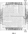
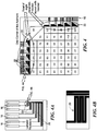
- an adaptive optic comprises a voltage-addressable, transmission-mode, liquid-crystal (LC) cell, as is generally known in the art, having substrates 12 patterned into an array of independent pixels generally denoted 14 to support two-dimensional (2-D) addressing for use as an AO actuator.
- LC liquid-crystal
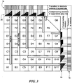
- each individual pixel in Figs. 1-4B is also provided having a unique alpha-numeric designation (e.g. A1 - A4; B1 - B12; C1 - C20, D1 - D28; E1 - E36, F1 - F44, G1 - G40).
- the adaptive optic is provided having a plurality of pixels having various shapes (squares and triangles) and arranged in columns and rows. Each of the pixels is coupled to a corresponding one of an output of a control circuit (not shown in Figs. 1-4B ).
- control circuits may be disposed on a substrate of the LC, via "flip-chip” or other chip-on-glass assembly technique, or else the control circuits may be "off-glass".
- the control circuits are coupled to pixels 14 via electrical signal paths which coupled control signals to conductors disposed on the substrate.
- each pixel 14 is individually addressable via the leads which are very narrow and are not clearly shown on the figures, but which run from each compensating resistor to its corresponding pixel, being routed in the narrow gaps between pixels.
- the control circuit(s) are capable of providing one or more control signals to each of the pixels of the AO.
- Each signal path coupled between the flex circuit and pixels includes an RC balancing resistor, generally denoted 20.
- the resistors are provided having a meander-resistor layout ( Fig. 4B ).
- the path lengths in the meander-resistor layout are selected so as to result in a substantially uniform speed in controlling pixels across the array. That is, the time it takes for any pixel in the AO pixel array to respond to a control signal is substantially the same regardless of pixel location within the AO.
- any effects (such as decrease of RMS voltage arising from delay and attenuation between the voltage source and the pixel) will be equalized across all pixels, enabling compensation for such voltage decrease in the calibration tables already needed for any liquid-crystal device.
- the AO includes a specially designed electrode layout which results in uniform time constants to all pixels across the aperture.
- a meander-resistor layout is used to achieve the desired uniform time constants.
- Each pixel has a capacitance which is known in advance, given its area and the device thickness as well as the properties of the liquid crystal, and thus resistors may be designed which make the product of R i C i the same, where i runs over for all pixels.
- the meander resistor chosen for this pixel would be of minimal resistance, preferably zero resistance, i.e., would be absent from the substrate layout.
- Compensating resistors 20 may be disposed in the superstrate glue line (i.e. a space into which sealant or "glue" is disposed to form sidewalls and couple a superstrate to a substrate) and resistors 20 are coupled via connecting elements 16 which provide a transition to leadouts (and eventually to flex circuits 18a, 18b and controllers) outside of the superstrate.
- the superstrate glue line i.e. a space into which sealant or "glue” is disposed to form sidewalls and couple a superstrate to a substrate
- connecting elements 16 which provide a transition to leadouts (and eventually to flex circuits 18a, 18b and controllers) outside of the superstrate.
- an electrode layout which results in uniform time constants to all pixels across the aperture is used,
- the pixels are square to better support the intended use of the AO with square beams.
- the concepts, systems and techniques described herein are not limited to square beams and that any beam shape may be used.
- an AO with a different pixel geometry than square may employ compensation resistors designed according to this teaching.
- a hexagonal close-packed array as is known in the art, a useful geometry for an AO.
- the feed lines for the pixels are of variable length, with longer ones for the central pixels, so the compensation resistor technique here taught is applicable for equalizing the response time and hence enabling more convenient drive voltage circuitry having the same calibration table for all pixels.
Claims (4)
- Adaptiver optischer Aktor, der Folgendes umfasst:ein Array aus Pixeln (14),wobei jedes der Pixel von einer Flüssigkristallzelle bereitgestellt wird, die Folgendes umfasst:ein Superstrat mit einer Innenoberfläche; ein Substrat (12) einer Innenoberfläche, die der Oberfläche des Superstrats gegenüberliegt; wobei das Substrat und Superstrat elektrisch leitfähige Strukturen aufweisen, die darauf gebildet sind und als Elektroden angeordnet sind, die ermöglichen, dass unterschiedliche Spannungen an jedes Pixel angelegt werden;mehrere elektrische Zuleitungen (16), wobei jede elektrische Zuleitung dazu in der Lage ist, ein oder mehrere Steuersignale zu führen, wobei jede elektrische Zuleitung mit einem einzigen Pixel in dem Array aus Pixeln gekoppelt ist; undmehrere Kompensationswiderstände (20), wobei jeder Kompensationswiderstand mit einer entsprechenden der mehreren elektrischen Zuleitungen verbunden ist, sodass eine im Wesentlichen gleichmäßige Zeitkonstante für alle Pixel über das Array aus Pixeln bereitgestellt wird.
- Adaptiver optischer Aktor nach Anspruch 1, wobei wenigstens manche der mehreren Kompensationswiderstände als Mäander-Widerstände bereitgestellt sind.
- Adaptiver optischer Aktor nach Anspruch 1, wobei die Flüssigkristallzelle als eine spannungsansteuerbare Transmissionsmodus-Flüssigkristallzelle bereitgestellt ist.
- Adaptiver optischer Aktor nach Anspruch 1, wobei wenigstens manche der Pixel mit einer Form bereitgestellt sind, die einer quadratischen Querschnittsform und/oder einer dreieckigen Querschnittsform entspricht.
Applications Claiming Priority (1)
| Application Number | Priority Date | Filing Date | Title |
|---|---|---|---|
| PCT/US2013/042638 WO2014189522A1 (en) | 2013-05-24 | 2013-05-24 | Adaptive - optics liquid - crystal array device having meander resistors |
Publications (2)
| Publication Number | Publication Date |
|---|---|
| EP3004979A1 EP3004979A1 (de) | 2016-04-13 |
| EP3004979B1 true EP3004979B1 (de) | 2019-01-16 |
Family
ID=48576602
Family Applications (1)
| Application Number | Title | Priority Date | Filing Date |
|---|---|---|---|
| EP13727011.2A Active EP3004979B1 (de) | 2013-05-24 | 2013-05-24 | Adaptiveoptik mit flüssigkristallanordnungsvorrichtung und mäanderwiderständen |
Country Status (8)
| Country | Link |
|---|---|
| US (1) | US9835856B2 (de) |
| EP (1) | EP3004979B1 (de) |
| JP (1) | JP6359088B2 (de) |
| AU (1) | AU2013389971B2 (de) |
| CA (1) | CA2910592C (de) |
| IL (1) | IL242306B (de) |
| NZ (1) | NZ713761A (de) |
| WO (1) | WO2014189522A1 (de) |
Families Citing this family (1)
| Publication number | Priority date | Publication date | Assignee | Title |
|---|---|---|---|---|
| US9971183B1 (en) | 2017-06-02 | 2018-05-15 | Raytheon Company | High power adaptive optic system and components therein |
Citations (2)
| Publication number | Priority date | Publication date | Assignee | Title |
|---|---|---|---|---|
| US20070285370A1 (en) * | 2006-06-08 | 2007-12-13 | Dong-Gyu Kim | Thin film transistor substrate and liquid crystal display panel having the same |
| WO2013073148A1 (ja) * | 2011-11-18 | 2013-05-23 | シャープ株式会社 | 光偏向素子 |
Family Cites Families (99)
| Publication number | Priority date | Publication date | Assignee | Title |
|---|---|---|---|---|
| US4482249A (en) | 1976-01-02 | 1984-11-13 | Raytheon Company | Electromagnetic wave ring resonator |
| US4141651A (en) | 1977-01-10 | 1979-02-27 | Raytheon Company | Laser gyroscope output optics structure |
| US4135789A (en) | 1977-07-01 | 1979-01-23 | Beckman Instruments, Inc. | Seal for liquid crystal display |
| US4548501A (en) | 1978-01-03 | 1985-10-22 | Raytheon Company | Laser gyroscope system |
| US4284329A (en) | 1978-01-03 | 1981-08-18 | Raytheon Company | Laser gyroscope system |
| US4229106A (en) | 1978-05-18 | 1980-10-21 | Raytheon Company | Electromagnetic wave ring resonator |
| US4525028A (en) | 1981-04-23 | 1985-06-25 | Raytheon Company | Enhanced magnetic mirror |
| US4418102A (en) | 1981-05-14 | 1983-11-29 | Eaton Corporation | Liquid crystal displays having improved hermetic seal |
| US4687331A (en) | 1982-05-19 | 1987-08-18 | Raytheon Company | Ring laser gyroscope |
| US4813774A (en) | 1982-08-27 | 1989-03-21 | Raytheon Company | Skewed rhombus ring laser gyro |
| US5412475A (en) | 1982-08-27 | 1995-05-02 | Raytheon Company | Diagonal pathlength control |
| US5333046A (en) | 1982-08-27 | 1994-07-26 | Raytheon Company | Diagonal pathlength control |
| US4818087A (en) | 1982-08-27 | 1989-04-04 | Raytheon Company | Orthohedral ring laser gyro |
| EP0112945B1 (de) | 1982-12-30 | 1987-05-06 | International Business Machines Corporation | Mit einer Flüssigkeit gefüllte Anzeigezelle und Verfahren zum Einfüllen und zur Siegelung einer solchen Zelle |
| DE3574292D1 (en) | 1985-01-02 | 1989-12-21 | Ibm | Electro-optic display cell and method of making same |
| US4695490A (en) | 1985-10-15 | 1987-09-22 | Rca Corporation | Seal for liquid crystal display |
| US5004343A (en) | 1986-03-14 | 1991-04-02 | Raytheon Company | Multiple ring paths in one block |
| US4964251A (en) | 1987-06-25 | 1990-10-23 | Allied-Signal Inc. | Dual-pane thermal window with liquid crystal shade |
| US5151814A (en) | 1987-08-19 | 1992-09-29 | Hughes Aircraft Company | Phased array for optical beam control |
| US4882235A (en) | 1988-03-02 | 1989-11-21 | Raytheon Company | Liquid crystal cell window |
| US4813766A (en) | 1988-03-02 | 1989-03-21 | Raytheon Company | Optical time delay apparatus |
| US4964701A (en) | 1988-10-04 | 1990-10-23 | Raytheon Company | Deflector for an optical beam |
| US5018835A (en) | 1989-01-03 | 1991-05-28 | Raytheon Company | Deflector for an optical beam including refractive means |
| US4943709A (en) | 1989-05-11 | 1990-07-24 | Hughes Aircraft Company | Liquid crystal adaptive optics system |
| JPH03164713A (ja) | 1989-11-24 | 1991-07-16 | Semiconductor Energy Lab Co Ltd | 強誘電性液晶電気光学装置とその作製方法 |
| US6545563B1 (en) | 1990-07-16 | 2003-04-08 | Raytheon Company | Digitally controlled monolithic microwave integrated circuits |
| US5126869A (en) | 1990-12-03 | 1992-06-30 | Raytheon Company | Two-dimensional, phased-array optical beam steerer |
| US5253033A (en) | 1990-12-03 | 1993-10-12 | Raytheon Company | Laser radar system with phased-array beam steerer |
| US5084898A (en) | 1990-12-18 | 1992-01-28 | Raytheon Company | Passive pathlength control mirror for laser |
| US5093740A (en) | 1991-02-28 | 1992-03-03 | Raytheon Company | Optical beam steerer having subaperture addressing |
| US5093747A (en) | 1991-02-28 | 1992-03-03 | Raytheon Company | Method for providing beam steering in a subaperture-addressed optical beam steerer |
| US5241995A (en) | 1991-09-24 | 1993-09-07 | Litton Systems Canada Limited | Method of filling a suspended particle display |
| US5246042A (en) | 1991-09-24 | 1993-09-21 | Litton Systems Canada Limited | Method of filling a suspended particle display |
| US5233673A (en) | 1991-10-09 | 1993-08-03 | Hughes Aircraft Company | Output steerable optical phased array |
| US5216729A (en) | 1991-11-18 | 1993-06-01 | Harmonic Lightwaves, Inc. | Active alignment system for laser to fiber coupling |
| US5276747A (en) | 1993-01-21 | 1994-01-04 | E-Tek Dynamics, Inc. | Polarization-independent optical switch/attenuator |
| US5363228A (en) | 1993-03-05 | 1994-11-08 | General Electric Company | Optical device with spatial light modulators for switching arbitrarily polarized light |
| JP3185831B2 (ja) | 1993-07-30 | 2001-07-11 | 富士写真フイルム株式会社 | 偏光コヒーレント合波レーザ |
| US6704474B1 (en) | 1994-05-24 | 2004-03-09 | Raytheon Company | Optical beam steering system |
| US5963682A (en) | 1994-05-24 | 1999-10-05 | Raytheon Company | Optical beam steering system |
| US5740288A (en) | 1995-02-22 | 1998-04-14 | E-Tek Dynamics, Inc. | Variable polarization beam splitter, combiner and mixer |
| US5898041A (en) | 1995-03-01 | 1999-04-27 | Matsushita Electric Industrial Co., Ltd. | Production process of liquid crystal display panel, seal material for liquid crystal cell and liquid crystal display |
| US6867888B2 (en) | 1996-07-12 | 2005-03-15 | Science Applications International Corporation | Switchable polymer-dispersed liquid crystal optical elements |
| JPH1048660A (ja) * | 1996-08-06 | 1998-02-20 | Toshiba Corp | 液晶表示装置 |
| US6103604A (en) | 1997-02-10 | 2000-08-15 | Trw Inc. | High electron mobility transparent conductor |
| AU747260B2 (en) | 1997-07-25 | 2002-05-09 | Nichia Chemical Industries, Ltd. | Nitride semiconductor device |
| US6282224B1 (en) | 1999-01-13 | 2001-08-28 | Raytheon Company | Non-planar Q-switched ring laser system |
| US6177903B1 (en) | 1999-06-14 | 2001-01-23 | Time Domain Corporation | System and method for intrusion detection using a time domain radar array |
| US6246369B1 (en) | 1999-09-14 | 2001-06-12 | Navsys Corporation | Miniature phased array antenna system |
| US6673497B2 (en) | 2000-01-04 | 2004-01-06 | University Of Central Florida | High efficiency volume diffractive elements in photo-thermo-refractive glass |
| JP3285341B2 (ja) | 2000-06-01 | 2002-05-27 | 士郎 酒井 | 窒化ガリウム系化合物半導体の製造方法 |
| FR2810415B1 (fr) | 2000-06-16 | 2002-12-06 | France Telecom | Aiguilleur optique a cristaux liquides a commande fiabilisee |
| JP3466144B2 (ja) | 2000-09-22 | 2003-11-10 | 士郎 酒井 | 半導体の表面を荒くする方法 |
| US6473148B1 (en) | 2000-11-28 | 2002-10-29 | Yafo Networks, Inc. | Seal pattern for liquid crystal device |
| US7088323B2 (en) * | 2000-12-21 | 2006-08-08 | Lg.Philips Lcd Co., Ltd. | Liquid crystal display device and method for fabricating the same |
| US6490076B2 (en) | 2001-01-11 | 2002-12-03 | Hrl Laboratories, Llc | Optical phased array for depolarized optical beam control |
| JP2002221730A (ja) * | 2001-01-24 | 2002-08-09 | Sony Corp | 液晶表示装置 |
| JP3585444B2 (ja) | 2001-02-05 | 2004-11-04 | ドーピー建設工業株式会社 | コンクリート部材の連結構造 |
| US6760512B2 (en) | 2001-06-08 | 2004-07-06 | Hrl Laboratories, Llc | Electro-optical programmable true-time delay generator |
| US6974517B2 (en) | 2001-06-13 | 2005-12-13 | Raytheon Company | Lid with window hermetically sealed to frame, and a method of making it |
| US6597836B2 (en) | 2001-06-20 | 2003-07-22 | The Boeing Company | Optical phased array control system |
| JP3548735B2 (ja) | 2001-06-29 | 2004-07-28 | 士郎 酒井 | 窒化ガリウム系化合物半導体の製造方法 |
| US6745449B2 (en) | 2001-11-06 | 2004-06-08 | Raytheon Company | Method and apparatus for making a lid with an optically transmissive window |
| US7005685B2 (en) | 2002-02-28 | 2006-02-28 | Shiro Sakai | Gallium-nitride-based compound semiconductor device |
| EP1502139A4 (de) | 2002-03-15 | 2005-06-29 | Pd Ld Inc | Faseroptische einrichtung mit volumen-bragg-gitter-elementen |
| JP4261123B2 (ja) * | 2002-04-30 | 2009-04-30 | 東芝松下ディスプレイテクノロジー株式会社 | 液晶表示装置 |
| KR100840330B1 (ko) * | 2002-08-07 | 2008-06-20 | 삼성전자주식회사 | 액정 표시 장치 및 이에 사용하는 구동 집적 회로 |
| US7166182B2 (en) | 2002-09-04 | 2007-01-23 | Sipix Imaging, Inc. | Adhesive and sealing layers for electrophoretic displays |
| US6988338B1 (en) | 2002-10-10 | 2006-01-24 | Raytheon Company | Lid with a thermally protected window |
| US7006747B2 (en) | 2003-01-17 | 2006-02-28 | 3M Innovative Properties Company | Optical devices incorporating photo reactive polymers |
| US7352428B2 (en) | 2003-02-21 | 2008-04-01 | Xtellus Inc. | Liquid crystal cell platform |
| US7355671B2 (en) | 2003-02-21 | 2008-04-08 | Xtellus Inc. | Fabrication method for liquid crystal cell |
| US6842200B1 (en) * | 2003-06-18 | 2005-01-11 | Hannstar Display Corporation | Liquid crystal panel having compensation capacitors for balancing RC delay effect |
| US6947627B2 (en) | 2003-09-30 | 2005-09-20 | Agilent Technologies, Inc. | Compact optical switches |
| US7196758B2 (en) | 2003-12-30 | 2007-03-27 | 3M Innovative Properties Company | Method of alignment of liquid crystals comprising exposing an alignment material to an interference pattern |
| US7215472B2 (en) | 2004-08-12 | 2007-05-08 | Raytheon Company | Wide-angle beam steering system |
| US7889767B2 (en) | 2004-10-13 | 2011-02-15 | Raytheon Company | Self-coherent combining technique for high power laser implementation and method |
| US7095925B2 (en) | 2004-11-03 | 2006-08-22 | Intel Corporation | Optical phased array transmitter/receiver |
| KR20060058987A (ko) * | 2004-11-26 | 2006-06-01 | 삼성전자주식회사 | 게이트 라인 구동 회로와, 이를 갖는 표시 장치와, 이의구동 장치 및 방법 |
| WO2006092758A2 (en) | 2005-03-01 | 2006-09-08 | Dutch Polymer Institute | Polarization gratings in mesogenic films |
| JP4617938B2 (ja) | 2005-03-16 | 2011-01-26 | 日立電線株式会社 | 光送信器 |
| US7226850B2 (en) | 2005-05-19 | 2007-06-05 | Raytheon Company | Gallium nitride high electron mobility transistor structure |
| EP1883381A4 (de) | 2005-05-25 | 2010-03-17 | Biolase Tech Inc | Elektromagnetische energieabgebende vorrichtung mit erhöhter punktgrösse |
| US20070030294A1 (en) * | 2005-08-05 | 2007-02-08 | Texas Instruments Incorporated | System and method for implementation of transition zone associated with an actuator for an optical device in a display system |
| JP2007114278A (ja) | 2005-10-18 | 2007-05-10 | Fuji Xerox Co Ltd | 光アドレス型空間光変調素子の駆動方法、および光アドレス型空間光変調素子駆動装置 |
| EP1962260A4 (de) | 2005-12-15 | 2010-08-18 | Sumitomo Electric Industries | Transparentes spinel-substrat, transparentes substrat für eine optische engine, rückprojektions-fernsehempfänger damit und bildprojektor mit flüssigkristall |
| JP5727120B2 (ja) * | 2006-08-25 | 2015-06-03 | 三星ディスプレイ株式會社Samsung Display Co.,Ltd. | 液晶表示装置 |
| US7557378B2 (en) | 2006-11-08 | 2009-07-07 | Raytheon Company | Boron aluminum nitride diamond heterostructure |
| KR20080050822A (ko) | 2006-12-04 | 2008-06-10 | 엘지디스플레이 주식회사 | 액정표시장치 |
| US7848370B2 (en) | 2007-01-26 | 2010-12-07 | Telaris Inc. | Electronically phase-locked laser systems |
| US7872838B2 (en) | 2007-02-09 | 2011-01-18 | Headway Technologies, Inc. | Uniformity in CCP magnetic read head devices |
| US20090044496A1 (en) | 2007-08-16 | 2009-02-19 | Botelho John W | Method and apparatus for sealing a glass package |
| KR100884998B1 (ko) * | 2007-08-29 | 2009-02-20 | 엘지디스플레이 주식회사 | 액정 표시 장치의 데이터 구동 장치 및 방법 |
| WO2009073158A1 (en) | 2007-11-30 | 2009-06-11 | Raytheon Company | Method and apparatus for maintaining a coherent combined beam during arbitrary steering |
| US8268707B2 (en) | 2009-06-22 | 2012-09-18 | Raytheon Company | Gallium nitride for liquid crystal electrodes |
| JP2013545124A (ja) | 2010-10-01 | 2013-12-19 | レイセオン カンパニー | 高充填比電子ビームステアリング |
| KR101917753B1 (ko) * | 2011-06-24 | 2018-11-13 | 가부시키가이샤 한도오따이 에네루기 켄큐쇼 | 표시 장치 |
| WO2013177519A1 (en) | 2012-05-24 | 2013-11-28 | Raytheon Company | Liquid crystal control structure, tip-tilt-focus optical phased array and high power adaptive optic |
| US20140268328A1 (en) | 2013-03-13 | 2014-09-18 | Raytheon Company | Polarization Grating Stack |
-
2013
- 2013-05-24 NZ NZ713761A patent/NZ713761A/en unknown
- 2013-05-24 CA CA2910592A patent/CA2910592C/en active Active
- 2013-05-24 WO PCT/US2013/042638 patent/WO2014189522A1/en active Application Filing
- 2013-05-24 JP JP2016513914A patent/JP6359088B2/ja active Active
- 2013-05-24 AU AU2013389971A patent/AU2013389971B2/en active Active
- 2013-05-24 EP EP13727011.2A patent/EP3004979B1/de active Active
- 2013-05-24 US US14/780,580 patent/US9835856B2/en active Active
-
2015
- 2015-10-27 IL IL242306A patent/IL242306B/en active IP Right Grant
Patent Citations (3)
| Publication number | Priority date | Publication date | Assignee | Title |
|---|---|---|---|---|
| US20070285370A1 (en) * | 2006-06-08 | 2007-12-13 | Dong-Gyu Kim | Thin film transistor substrate and liquid crystal display panel having the same |
| WO2013073148A1 (ja) * | 2011-11-18 | 2013-05-23 | シャープ株式会社 | 光偏向素子 |
| US20140267965A1 (en) * | 2011-11-18 | 2014-09-18 | Sharp Kabushiki Kaisha | Optical deflector |
Also Published As
| Publication number | Publication date |
|---|---|
| US20160077333A1 (en) | 2016-03-17 |
| EP3004979A1 (de) | 2016-04-13 |
| JP2016521010A (ja) | 2016-07-14 |
| WO2014189522A1 (en) | 2014-11-27 |
| NZ713761A (en) | 2017-05-26 |
| CA2910592A1 (en) | 2014-11-27 |
| JP6359088B2 (ja) | 2018-07-18 |
| AU2013389971B2 (en) | 2017-03-09 |
| IL242306B (en) | 2020-11-30 |
| US9835856B2 (en) | 2017-12-05 |
| CA2910592C (en) | 2017-11-21 |
| AU2013389971A1 (en) | 2015-11-12 |
Similar Documents
| Publication | Publication Date | Title |
|---|---|---|
| EP3182200B1 (de) | Lichtmodulationsvorrichtung einschliesslich einer dielektrischen antenne | |
| EP3157100A2 (de) | Phasengesteuertes gruppenantennensystem mit einer modularen steuerung und überwachungsarchitektur | |
| US20070069999A1 (en) | Spatial light modulator employing voltage gradient pixels, and associated methods | |
| EP3004979B1 (de) | Adaptiveoptik mit flüssigkristallanordnungsvorrichtung und mäanderwiderständen | |
| CN108845416B (zh) | 光路径调整装置以及显示器件 | |
| KR20160103600A (ko) | 표시 장치 | |
| CN103149682A (zh) | 用于波前相位校正的光控变形镜装置 | |
| EP2856250B1 (de) | Flüssigkristall-steuerungsstruktur, optisches tip-tilt-fokus-phasenarray und adaptive hochleistungsoptik | |
| JP2019070764A (ja) | 位相変調装置 | |
| US20130088682A1 (en) | Controllable optical device and the forming method thereof | |
| JP2018136567A (ja) | 蛇行抵抗器を有する適応光学液晶アレイデバイス | |
| EP3696598B1 (de) | Phasenmodulator | |
| JP2020086210A5 (de) | ||
| US11506824B2 (en) | Circuit for controlling liquid lens | |
| CN111146588B (zh) | 相控阵天线 | |
| US9471174B2 (en) | Control apparatus and method of addressing two-dimensional signal | |
| EP2015125A1 (de) | Optisch angesteuerter verformbarer Spiegel | |
| KR101882734B1 (ko) | 전기 영동 표시 장치 | |
| JP2016521010A5 (de) | ||
| KR102245987B1 (ko) | 미러의 자체 각도 조절 기능을 갖는 광 스캐너 및 그의 미러 각도 조절 방법 | |
| WO2016079955A1 (ja) | 光導波路用ヒータ及び光導波路用ヒータの構成方法 | |
| JP5319411B2 (ja) | ミラー装置およびミラーアレイ | |
| KR102362731B1 (ko) | 액체 렌즈 제어 회로 | |
| EP2339391A1 (de) | Betätigungseinrichtung für ein adaptatives optisches Instrument | |
| JP5519614B2 (ja) | 光通信装置およびミラー素子 |
Legal Events
| Date | Code | Title | Description |
|---|---|---|---|
| PUAI | Public reference made under article 153(3) epc to a published international application that has entered the european phase |
Free format text: ORIGINAL CODE: 0009012 |
|
| 17P | Request for examination filed |
Effective date: 20151203 |
|
| AK | Designated contracting states |
Kind code of ref document: A1 Designated state(s): AL AT BE BG CH CY CZ DE DK EE ES FI FR GB GR HR HU IE IS IT LI LT LU LV MC MK MT NL NO PL PT RO RS SE SI SK SM TR |
|
| AX | Request for extension of the european patent |
Extension state: BA ME |
|
| DAX | Request for extension of the european patent (deleted) | ||
| REG | Reference to a national code |
Ref country code: DE Ref legal event code: R079 Ref document number: 602013049869 Country of ref document: DE Free format text: PREVIOUS MAIN CLASS: G02F0001134500 Ipc: G02F0001134300 |
|
| GRAP | Despatch of communication of intention to grant a patent |
Free format text: ORIGINAL CODE: EPIDOSNIGR1 |
|
| STAA | Information on the status of an ep patent application or granted ep patent |
Free format text: STATUS: GRANT OF PATENT IS INTENDED |
|
| RIC1 | Information provided on ipc code assigned before grant |
Ipc: G02F 1/1343 20060101AFI20180731BHEP Ipc: G02F 1/29 20060101ALI20180731BHEP |
|
| INTG | Intention to grant announced |
Effective date: 20180817 |
|
| GRAS | Grant fee paid |
Free format text: ORIGINAL CODE: EPIDOSNIGR3 |
|
| GRAA | (expected) grant |
Free format text: ORIGINAL CODE: 0009210 |
|
| STAA | Information on the status of an ep patent application or granted ep patent |
Free format text: STATUS: THE PATENT HAS BEEN GRANTED |
|
| AK | Designated contracting states |
Kind code of ref document: B1 Designated state(s): AL AT BE BG CH CY CZ DE DK EE ES FI FR GB GR HR HU IE IS IT LI LT LU LV MC MK MT NL NO PL PT RO RS SE SI SK SM TR |
|
| REG | Reference to a national code |
Ref country code: GB Ref legal event code: FG4D |
|
| REG | Reference to a national code |
Ref country code: CH Ref legal event code: EP |
|
| REG | Reference to a national code |
Ref country code: IE Ref legal event code: FG4D |
|
| REG | Reference to a national code |
Ref country code: DE Ref legal event code: R096 Ref document number: 602013049869 Country of ref document: DE |
|
| REG | Reference to a national code |
Ref country code: AT Ref legal event code: REF Ref document number: 1090146 Country of ref document: AT Kind code of ref document: T Effective date: 20190215 |
|
| REG | Reference to a national code |
Ref country code: NL Ref legal event code: MP Effective date: 20190116 |
|
| REG | Reference to a national code |
Ref country code: LT Ref legal event code: MG4D |
|
| PG25 | Lapsed in a contracting state [announced via postgrant information from national office to epo] |
Ref country code: NL Free format text: LAPSE BECAUSE OF FAILURE TO SUBMIT A TRANSLATION OF THE DESCRIPTION OR TO PAY THE FEE WITHIN THE PRESCRIBED TIME-LIMIT Effective date: 20190116 |
|
| REG | Reference to a national code |
Ref country code: AT Ref legal event code: MK05 Ref document number: 1090146 Country of ref document: AT Kind code of ref document: T Effective date: 20190116 |
|
| PG25 | Lapsed in a contracting state [announced via postgrant information from national office to epo] |
Ref country code: PT Free format text: LAPSE BECAUSE OF FAILURE TO SUBMIT A TRANSLATION OF THE DESCRIPTION OR TO PAY THE FEE WITHIN THE PRESCRIBED TIME-LIMIT Effective date: 20190516 Ref country code: SE Free format text: LAPSE BECAUSE OF FAILURE TO SUBMIT A TRANSLATION OF THE DESCRIPTION OR TO PAY THE FEE WITHIN THE PRESCRIBED TIME-LIMIT Effective date: 20190116 Ref country code: FI Free format text: LAPSE BECAUSE OF FAILURE TO SUBMIT A TRANSLATION OF THE DESCRIPTION OR TO PAY THE FEE WITHIN THE PRESCRIBED TIME-LIMIT Effective date: 20190116 Ref country code: PL Free format text: LAPSE BECAUSE OF FAILURE TO SUBMIT A TRANSLATION OF THE DESCRIPTION OR TO PAY THE FEE WITHIN THE PRESCRIBED TIME-LIMIT Effective date: 20190116 Ref country code: NO Free format text: LAPSE BECAUSE OF FAILURE TO SUBMIT A TRANSLATION OF THE DESCRIPTION OR TO PAY THE FEE WITHIN THE PRESCRIBED TIME-LIMIT Effective date: 20190416 Ref country code: ES Free format text: LAPSE BECAUSE OF FAILURE TO SUBMIT A TRANSLATION OF THE DESCRIPTION OR TO PAY THE FEE WITHIN THE PRESCRIBED TIME-LIMIT Effective date: 20190116 Ref country code: LT Free format text: LAPSE BECAUSE OF FAILURE TO SUBMIT A TRANSLATION OF THE DESCRIPTION OR TO PAY THE FEE WITHIN THE PRESCRIBED TIME-LIMIT Effective date: 20190116 |
|
| PG25 | Lapsed in a contracting state [announced via postgrant information from national office to epo] |
Ref country code: HR Free format text: LAPSE BECAUSE OF FAILURE TO SUBMIT A TRANSLATION OF THE DESCRIPTION OR TO PAY THE FEE WITHIN THE PRESCRIBED TIME-LIMIT Effective date: 20190116 Ref country code: GR Free format text: LAPSE BECAUSE OF FAILURE TO SUBMIT A TRANSLATION OF THE DESCRIPTION OR TO PAY THE FEE WITHIN THE PRESCRIBED TIME-LIMIT Effective date: 20190417 Ref country code: IS Free format text: LAPSE BECAUSE OF FAILURE TO SUBMIT A TRANSLATION OF THE DESCRIPTION OR TO PAY THE FEE WITHIN THE PRESCRIBED TIME-LIMIT Effective date: 20190516 Ref country code: LV Free format text: LAPSE BECAUSE OF FAILURE TO SUBMIT A TRANSLATION OF THE DESCRIPTION OR TO PAY THE FEE WITHIN THE PRESCRIBED TIME-LIMIT Effective date: 20190116 Ref country code: BG Free format text: LAPSE BECAUSE OF FAILURE TO SUBMIT A TRANSLATION OF THE DESCRIPTION OR TO PAY THE FEE WITHIN THE PRESCRIBED TIME-LIMIT Effective date: 20190416 Ref country code: RS Free format text: LAPSE BECAUSE OF FAILURE TO SUBMIT A TRANSLATION OF THE DESCRIPTION OR TO PAY THE FEE WITHIN THE PRESCRIBED TIME-LIMIT Effective date: 20190116 |
|
| REG | Reference to a national code |
Ref country code: DE Ref legal event code: R097 Ref document number: 602013049869 Country of ref document: DE |
|
| PG25 | Lapsed in a contracting state [announced via postgrant information from national office to epo] |
Ref country code: SK Free format text: LAPSE BECAUSE OF FAILURE TO SUBMIT A TRANSLATION OF THE DESCRIPTION OR TO PAY THE FEE WITHIN THE PRESCRIBED TIME-LIMIT Effective date: 20190116 Ref country code: RO Free format text: LAPSE BECAUSE OF FAILURE TO SUBMIT A TRANSLATION OF THE DESCRIPTION OR TO PAY THE FEE WITHIN THE PRESCRIBED TIME-LIMIT Effective date: 20190116 Ref country code: CZ Free format text: LAPSE BECAUSE OF FAILURE TO SUBMIT A TRANSLATION OF THE DESCRIPTION OR TO PAY THE FEE WITHIN THE PRESCRIBED TIME-LIMIT Effective date: 20190116 Ref country code: DK Free format text: LAPSE BECAUSE OF FAILURE TO SUBMIT A TRANSLATION OF THE DESCRIPTION OR TO PAY THE FEE WITHIN THE PRESCRIBED TIME-LIMIT Effective date: 20190116 Ref country code: IT Free format text: LAPSE BECAUSE OF FAILURE TO SUBMIT A TRANSLATION OF THE DESCRIPTION OR TO PAY THE FEE WITHIN THE PRESCRIBED TIME-LIMIT Effective date: 20190116 Ref country code: AT Free format text: LAPSE BECAUSE OF FAILURE TO SUBMIT A TRANSLATION OF THE DESCRIPTION OR TO PAY THE FEE WITHIN THE PRESCRIBED TIME-LIMIT Effective date: 20190116 Ref country code: EE Free format text: LAPSE BECAUSE OF FAILURE TO SUBMIT A TRANSLATION OF THE DESCRIPTION OR TO PAY THE FEE WITHIN THE PRESCRIBED TIME-LIMIT Effective date: 20190116 Ref country code: AL Free format text: LAPSE BECAUSE OF FAILURE TO SUBMIT A TRANSLATION OF THE DESCRIPTION OR TO PAY THE FEE WITHIN THE PRESCRIBED TIME-LIMIT Effective date: 20190116 |
|
| PLBE | No opposition filed within time limit |
Free format text: ORIGINAL CODE: 0009261 |
|
| STAA | Information on the status of an ep patent application or granted ep patent |
Free format text: STATUS: NO OPPOSITION FILED WITHIN TIME LIMIT |
|
| PG25 | Lapsed in a contracting state [announced via postgrant information from national office to epo] |
Ref country code: SM Free format text: LAPSE BECAUSE OF FAILURE TO SUBMIT A TRANSLATION OF THE DESCRIPTION OR TO PAY THE FEE WITHIN THE PRESCRIBED TIME-LIMIT Effective date: 20190116 |
|
| 26N | No opposition filed |
Effective date: 20191017 |
|
| REG | Reference to a national code |
Ref country code: CH Ref legal event code: PL |
|
| PG25 | Lapsed in a contracting state [announced via postgrant information from national office to epo] |
Ref country code: CH Free format text: LAPSE BECAUSE OF NON-PAYMENT OF DUE FEES Effective date: 20190531 Ref country code: LI Free format text: LAPSE BECAUSE OF NON-PAYMENT OF DUE FEES Effective date: 20190531 Ref country code: MC Free format text: LAPSE BECAUSE OF FAILURE TO SUBMIT A TRANSLATION OF THE DESCRIPTION OR TO PAY THE FEE WITHIN THE PRESCRIBED TIME-LIMIT Effective date: 20190116 |
|
| REG | Reference to a national code |
Ref country code: BE Ref legal event code: MM Effective date: 20190531 |
|
| PG25 | Lapsed in a contracting state [announced via postgrant information from national office to epo] |
Ref country code: SI Free format text: LAPSE BECAUSE OF FAILURE TO SUBMIT A TRANSLATION OF THE DESCRIPTION OR TO PAY THE FEE WITHIN THE PRESCRIBED TIME-LIMIT Effective date: 20190116 Ref country code: LU Free format text: LAPSE BECAUSE OF NON-PAYMENT OF DUE FEES Effective date: 20190524 |
|
| PG25 | Lapsed in a contracting state [announced via postgrant information from national office to epo] |
Ref country code: TR Free format text: LAPSE BECAUSE OF FAILURE TO SUBMIT A TRANSLATION OF THE DESCRIPTION OR TO PAY THE FEE WITHIN THE PRESCRIBED TIME-LIMIT Effective date: 20190116 |
|
| PG25 | Lapsed in a contracting state [announced via postgrant information from national office to epo] |
Ref country code: IE Free format text: LAPSE BECAUSE OF NON-PAYMENT OF DUE FEES Effective date: 20190524 |
|
| PG25 | Lapsed in a contracting state [announced via postgrant information from national office to epo] |
Ref country code: BE Free format text: LAPSE BECAUSE OF NON-PAYMENT OF DUE FEES Effective date: 20190531 |
|
| PG25 | Lapsed in a contracting state [announced via postgrant information from national office to epo] |
Ref country code: CY Free format text: LAPSE BECAUSE OF FAILURE TO SUBMIT A TRANSLATION OF THE DESCRIPTION OR TO PAY THE FEE WITHIN THE PRESCRIBED TIME-LIMIT Effective date: 20190116 |
|
| PG25 | Lapsed in a contracting state [announced via postgrant information from national office to epo] |
Ref country code: MT Free format text: LAPSE BECAUSE OF FAILURE TO SUBMIT A TRANSLATION OF THE DESCRIPTION OR TO PAY THE FEE WITHIN THE PRESCRIBED TIME-LIMIT Effective date: 20190116 Ref country code: HU Free format text: LAPSE BECAUSE OF FAILURE TO SUBMIT A TRANSLATION OF THE DESCRIPTION OR TO PAY THE FEE WITHIN THE PRESCRIBED TIME-LIMIT; INVALID AB INITIO Effective date: 20130524 |
|
| PG25 | Lapsed in a contracting state [announced via postgrant information from national office to epo] |
Ref country code: MK Free format text: LAPSE BECAUSE OF FAILURE TO SUBMIT A TRANSLATION OF THE DESCRIPTION OR TO PAY THE FEE WITHIN THE PRESCRIBED TIME-LIMIT Effective date: 20190116 |
|
| P01 | Opt-out of the competence of the unified patent court (upc) registered |
Effective date: 20230530 |
|
| PGFP | Annual fee paid to national office [announced via postgrant information from national office to epo] |
Ref country code: FR Payment date: 20230420 Year of fee payment: 11 Ref country code: DE Payment date: 20230419 Year of fee payment: 11 |
|
| PGFP | Annual fee paid to national office [announced via postgrant information from national office to epo] |
Ref country code: GB Payment date: 20230420 Year of fee payment: 11 |