EP2997406B1 - Verfahren zur herstellung von in ein gehäuse hermetisch dicht einlötbaren fensterelementen und danach hergestellte freiformfensterelemente - Google Patents
Verfahren zur herstellung von in ein gehäuse hermetisch dicht einlötbaren fensterelementen und danach hergestellte freiformfensterelemente Download PDFInfo
- Publication number
- EP2997406B1 EP2997406B1 EP14741504.6A EP14741504A EP2997406B1 EP 2997406 B1 EP2997406 B1 EP 2997406B1 EP 14741504 A EP14741504 A EP 14741504A EP 2997406 B1 EP2997406 B1 EP 2997406B1
- Authority
- EP
- European Patent Office
- Prior art keywords
- carrier material
- layer
- window elements
- edge region
- optical coating
- Prior art date
- Legal status (The legal status is an assumption and is not a legal conclusion. Google has not performed a legal analysis and makes no representation as to the accuracy of the status listed.)
- Active
Links
Images


Classifications
-
- G—PHYSICS
- G02—OPTICS
- G02B—OPTICAL ELEMENTS, SYSTEMS OR APPARATUS
- G02B27/00—Optical systems or apparatus not provided for by any of the groups G02B1/00 - G02B26/00, G02B30/00
- G02B27/02—Viewing or reading apparatus
- G02B27/022—Viewing apparatus
-
- G—PHYSICS
- G01—MEASURING; TESTING
- G01J—MEASUREMENT OF INTENSITY, VELOCITY, SPECTRAL CONTENT, POLARISATION, PHASE OR PULSE CHARACTERISTICS OF INFRARED, VISIBLE OR ULTRAVIOLET LIGHT; COLORIMETRY; RADIATION PYROMETRY
- G01J5/00—Radiation pyrometry, e.g. infrared or optical thermometry
- G01J5/02—Constructional details
- G01J5/08—Optical arrangements
- G01J5/0875—Windows; Arrangements for fastening thereof
-
- G—PHYSICS
- G01—MEASURING; TESTING
- G01J—MEASUREMENT OF INTENSITY, VELOCITY, SPECTRAL CONTENT, POLARISATION, PHASE OR PULSE CHARACTERISTICS OF INFRARED, VISIBLE OR ULTRAVIOLET LIGHT; COLORIMETRY; RADIATION PYROMETRY
- G01J1/00—Photometry, e.g. photographic exposure meter
- G01J1/02—Details
- G01J1/0271—Housings; Attachments or accessories for photometers
-
- G—PHYSICS
- G01—MEASURING; TESTING
- G01J—MEASUREMENT OF INTENSITY, VELOCITY, SPECTRAL CONTENT, POLARISATION, PHASE OR PULSE CHARACTERISTICS OF INFRARED, VISIBLE OR ULTRAVIOLET LIGHT; COLORIMETRY; RADIATION PYROMETRY
- G01J5/00—Radiation pyrometry, e.g. infrared or optical thermometry
- G01J5/02—Constructional details
- G01J5/04—Casings
- G01J5/041—Mountings in enclosures or in a particular environment
- G01J5/045—Sealings; Vacuum enclosures; Encapsulated packages; Wafer bonding structures; Getter arrangements
-
- G—PHYSICS
- G02—OPTICS
- G02B—OPTICAL ELEMENTS, SYSTEMS OR APPARATUS
- G02B1/00—Optical elements characterised by the material of which they are made; Optical coatings for optical elements
- G02B1/02—Optical elements characterised by the material of which they are made; Optical coatings for optical elements made of crystals, e.g. rock-salt, semi-conductors
-
- G—PHYSICS
- G02—OPTICS
- G02B—OPTICAL ELEMENTS, SYSTEMS OR APPARATUS
- G02B1/00—Optical elements characterised by the material of which they are made; Optical coatings for optical elements
- G02B1/10—Optical coatings produced by application to, or surface treatment of, optical elements
-
- G—PHYSICS
- G02—OPTICS
- G02B—OPTICAL ELEMENTS, SYSTEMS OR APPARATUS
- G02B27/00—Optical systems or apparatus not provided for by any of the groups G02B1/00 - G02B26/00, G02B30/00
- G02B27/02—Viewing or reading apparatus
- G02B27/028—Viewing or reading apparatus characterised by the supporting structure
-
- G—PHYSICS
- G02—OPTICS
- G02B—OPTICAL ELEMENTS, SYSTEMS OR APPARATUS
- G02B7/00—Mountings, adjusting means, or light-tight connections, for optical elements
- G02B7/007—Pressure-resistant sight glasses
-
- H—ELECTRICITY
- H10—SEMICONDUCTOR DEVICES; ELECTRIC SOLID-STATE DEVICES NOT OTHERWISE PROVIDED FOR
- H10F—INORGANIC SEMICONDUCTOR DEVICES SENSITIVE TO INFRARED RADIATION, LIGHT, ELECTROMAGNETIC RADIATION OF SHORTER WAVELENGTH OR CORPUSCULAR RADIATION
- H10F77/00—Constructional details of devices covered by this subclass
- H10F77/40—Optical elements or arrangements
- H10F77/407—Optical elements or arrangements indirectly associated with the devices
-
- C—CHEMISTRY; METALLURGY
- C09—DYES; PAINTS; POLISHES; NATURAL RESINS; ADHESIVES; COMPOSITIONS NOT OTHERWISE PROVIDED FOR; APPLICATIONS OF MATERIALS NOT OTHERWISE PROVIDED FOR
- C09K—MATERIALS FOR MISCELLANEOUS APPLICATIONS, NOT PROVIDED FOR ELSEWHERE
- C09K13/00—Etching, surface-brightening or pickling compositions
Definitions
- the invention relates to a method for the production of window elements which can be soldered into a housing in a hermetically sealed manner and which have an optical coating and to freeform window elements produced according to the method.
- Window elements of this type are particularly suitable for hermetically sealing (vacuum-tight) housings of radiation detectors or sources while ensuring optical, in particular spectral, functions.
- window elements produced in this way result from frame-shaped partial areas which, due to their rectangular shape, can be processed well, but are limited in terms of their restriction of the radiation angle in the case of sensors or detectors with a minimized area.
- the window elements produced in this way lead to limitations in adapting to the existing housing and to quality losses in the case of small-dimensioned area sensors or image detectors.
- an optoelectronic semiconductor module which is equipped with a light-emitting semiconductor chip mounted on a chip carrier and a cover element which has an at least partially permeable cover plate over the semiconductor chip, and a frame part for lateral sheathing of the semiconductor chip, the cover plate and frame part being connected to one another without a joint by anodic bonding are.
- the frame part and the chip carrier can then be connected by soldering in the same way as conventional metallic chip carriers and caps.
- document JP2009276691 describes a method for producing a window element equipped with optical filters, in which the optical layers are covered with a protective layer before the rectangular window elements are mechanically separated, an edge area of the window surrounding the filter layers is removed and a metal layer over the entire window surface including the protective layer is applied. Together with the protective layer dissolved by a solvent, the metal layer over the optical layers is also removed, but remains on the substrate edge, on which a parting line is created in the substrate by means of a grinding wheel.
- the invention is based on the object of finding an improved way of producing optical window elements with an optical coating that can be hermetically soldered into a housing and that provide a permanently reliable hermetically gas-tight or vacuum-tight soldered connection to a metallic housing, even under alternating thermal loads allow and continue to keep the penetration of scattered and interfering radiation into the layer system of the optical coating low.
- window elements with flexible shape variants (free-form windows) made of optically transparent, flat carrier material, which can be manufactured cost-effectively in a desired small format in the range between 1 mm and 100 mm, can be soldered hermetically (vacuum-tight) and are permanently stable for the above Applications are.
- free-form surfaces of optical windows are understood to mean those window elements which - with a flat basic shape, preferably plane-parallel, but in special cases also with integrated optical lenses and / or filter functions - are round, oval, sickle-shaped, polygonal, for example triangular, rectangular, polygonal, but also semicircular, third- or quarter-circular, etc., with all shapes also preferably being able to be designed with rounded corners.
- the outline shape can also be designed in a freely definable form in accordance with a purpose of the window elements.
- the object is achieved in a method for producing window elements that can be soldered in a housing in a hermetically sealed manner by the features according to claim 1.
- a laser beam, a particle beam or an electron beam can advantageously be used as the directed machining beam.
- the directed machining beam of high-energy radiation is used to remove the locally machined peripheral edge area of the carrier material, which has at least one lowered step in an inner and a further step in an outer edge area with rounded edges with radii R between 50 and 150 ⁇ m, in order to obtain, in step e), through the complete coating with the solder layer system, a low-tension metallization of the locally processed peripheral edge area as well as an additional edge wrap for a later applied solder of the solder layer.
- the cleaning process can preferably be carried out by beam processing using a laser beam, particle beam, electron beam, glass bead beam or etching liquid beam.
- a large number of window elements are preferably produced on the wafer-shaped carrier material.
- step f) of detaching the metallization from the optical coating the individual window elements are cut out of the carrier material along separating lines.
- the individual window elements can also be cut out of the carrier material along the dividing lines immediately afterwards.
- the window elements are expediently cut out by severing the carrier material along the dividing lines from the front side, the front side being the surface of the carrier material provided for the solderable metallization.
- a holding substrate can additionally be provided and the carrier material can be attached to the holding substrate by means of an adhesive for each window element.
- the window elements can expediently be cut out by means of a directed machining beam of high-energy radiation by repeatedly crossing the separating lines with the directed machining beam, and at the same time rounded edges with desired radii R can be produced along the separating lines.
- the window elements can be cut out by repeatedly crossing the dividing lines with the directional processing beam directly in connection with the removal of the lowered step of the carrier material generated by the directional processing beam, and the rounded edges with the radii R in the double up to the three-digit micrometer range can be generated along the dividing lines.
- a silicon nitride, zinc sulfide or DLC (diamond-like carbon) layer or a layer made of an oxide of silicon, magnesium, aluminum can advantageously be used as a final layer of the optical coating or a layer made of a fluoride of yttrium, ytterbium, barium or a semiconductor layer made of germanium or silicon can be used.
- a metallic protective layer is preferably applied to the optical coating as a protective layer and lift-off make.
- the protective layer can be produced with at least one of the metallic materials from the group consisting of aluminum and aluminum alloys, such as aluminum-silicon, aluminum-magnesium, aluminum-lithium alloys, and nickel and nickel-iron alloys.
- the metallic protective layer can be supplemented by a polymer layer before it is covered with the solder layer system if the lift-off process is to be facilitated in the case of thick solder layer systems.
- a polymer layer e.g. a photoresist layer
- the freeform window elements produced according to one or more of the preceding production variants for openings of any shape in a housing are preferably used to produce gas- or vacuum-tight optoelectronic or electro-optical components.
- the invention is based on the empirical knowledge that the known additional adhesion promoter layers for increasing the reliability of the hermetically sealed soldered connection do not produce the desired permanent success under alternating thermal loads, so that the permanent guarantee of tightness of the Housing-window connection, an even closer contact of the soldering coating on the window material must be established, which also does not put additional technological strain on the optical filter layers and continues to keep the undesired extraneous radiation (scattered and other interference radiation) from the edge of the filter system low.
- the shape of the window should not be restricted to rectangular, square or circular windows, as was previously the case.
- these problems are solved by removing the optical coating in the edge area by beam processing with a high-energy beam (laser, electron or particle beam) right into the substrate of the window (removal of a substrate step of more than the thickness of the optical coating) takes place, which at the same time allows the production of any free-form surfaces with a material removal "circumscribing" the desired optically effective surface, and with a defined remaining surface roughness of the removal enables a direct application of the metallization with the solder layer system.
- a high-energy beam laser, electron or particle beam
- the invention allows the production of optical window elements that ensure a permanently reliable - even with thermal alternating load - hermetically gas- or vacuum-tight soldered connection with a metallic housing and also keep the penetration of scattered and interfering radiation into the optical layer system low.
- the type of edge removal also enables the production of free-form window surfaces, which at the same time increases the long-term stability of the soldered connection.
- the carrier material 1 used is preferably silicon, germanium, barium fluoride, calcium fluoride, zinc sulfide or even sapphire (only transparent up to 5.5 ⁇ m).
- Optical coatings can be of a wide variety of types. They range from anti-reflective coating systems (e.g. AR filter 21) to a wide variety of spectral edge and bandpass filters to interference filter systems with very special spectral characteristics (summarized below as spectral filter system 22 or abstracted as optical coating 2).
- the latter interference filter systems are preferably applied to the (technological) top side of the window element 6, which also carries the metallization 7 for the soldered connection, which later represents the inside of the window element 6 in the housing 9.
- the (technological) rear side of the window element 6, which is later installed as the outside on the housing 9, is more often - but not exclusively - covered with anti-reflective coatings, absorption filters and reflection filters.
- materials such as aluminum and alloys with it (e.g. Al-Si, Al-Mg, Al-Li) or also nickel and nickel-iron alloys are used, whereby large layer thicknesses (between 100 nm and 5 ⁇ m) for sufficient layer stability and short etching times (between 1 min and 10 min, ideally 2 - 3 min) are preferred for the lift-off process.
- alternative Protective layers 3 made of chromium or titanium only require smaller layer thicknesses (between 50 nm and 1 ⁇ m).
- the protective layer 3 For the layer removal by the machining beam 4, however, greater layer thicknesses of the protective layer 3 of up to 8 ⁇ m are sometimes required in order to provide sufficient protection (e.g. against plasma splashes). In such cases, thicker polymer layers (e.g. photoresist) or a composite of the aforementioned metal and polymer layers can also be formed.
- thicker polymer layers e.g. photoresist
- a composite of the aforementioned metal and polymer layers can also be formed.
- the continued gradual removal of material from the carrier material 1 by means of the processing beam 4 is an essential process step.
- a defined roughness of the edge area 62 is created around the desired optically effective free-form surface 61, which is set as homogeneously as possible in the range between 0.5 ⁇ m and 2.5 ⁇ m in order to enable the solder layer system 71 to adhere reliably and permanently.
- the homogeneity is achieved by circling, parallel to the edge, the removal lines of the machining beam 4 around the optically effective free-form surface 61.
- the removal of at least one step 11, which is lowered more than the layer thickness of the optical coating 2 below the base level of the optical coating 2, ensures that later interference light coupling from the edge area 62 of the metallization 7 into the optical coating 2 is largely suppressed.
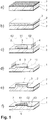
- window elements 6 Since the production of window elements 6 is always about technological effectiveness, the individual window elements 6 also have to be cut out for the production of a large number of different window elements 6 on a common carrier material 1 (so-called wafer) Make the coating and removal process can be done. For this purpose, different possibilities are given in the following process variants.
- Exemplary parameters of a laser beam for layer removal are preferably a spot diameter of 30 ⁇ m to 60 ⁇ m, a pulse frequency of 1 kHz to 1000 kHz with a laser power of 5 W to 60 W.
- a spot diameter of 30 ⁇ m to 60 ⁇ m preferably a spot diameter of 30 ⁇ m to 60 ⁇ m, a pulse frequency of 1 kHz to 1000 kHz with a laser power of 5 W to 60 W.
- the protective layer 3 for the optically effective free-form surfaces 61 is in a first embodiment a metallic protective layer 3, preferably made of aluminum (Al), which under defined process conditions during sputtering (e.g. substrate temperature ⁇ 180 ° C and relatively high working pressures of 1.066 Pa ⁇ p ⁇ 2.250 Pa) is deposited in layer thicknesses of 0.5 ⁇ m to 5 ⁇ m in order to produce a coarsely crystalline structure.
- Al aluminum
- This structure is decorated by etching, if necessary, so that the aluminum in the range of the laser light wavelength (preferably 1 ⁇ m) has a low reflectivity due to the surface roughness that has arisen.
- the protective layer 3 which can have a total thickness of up to three to five times the thickness of the solder layer system 71 for the formation of an effective lift-off mask, the contamination from laser smoke and plasma splashes that usually occur in the laser process is prevented and through Undercut the protective layer 3n is used as a lift-off mask in order to detach the metallization 7 above the optical coating 2.
- a pure Al layer with thicknesses of> 100 nm and ⁇ 5 ⁇ m will be used.
- a polymer layer for example known photoresist
- a composite of metal and polymer can also be used as materials for the protective layer 3.
- aluminum alloys such as aluminum-silicon, aluminum-magnesium or aluminum-lithium alloys
- nickel and nickel-iron alloys can also be used for metallic protective layers 3.
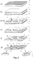
- Possible free-form variants of the window elements 6 are based on Figures 2 to 6 to recognize. It goes without saying that combinations of the shapes of the window elements 6 and the shapes of the carrier material 1 (wafers or plates in the range from 0.2 mm to 6 mm thick with optical coatings 2 for UV light, IR light and visible light) are possible and are encompassed by the disclosed subject matter of the invention.
- the selected utility technology for optimal use of space is useful or sufficient for cutting out the individual window elements 6 web widths between 0.5 mm and 1 mm if the proposed beam processing also involves cutting out with a processing beam 4 of high-energy radiation (e.g. laser beam).
- a processing beam 4 of high-energy radiation e.g. laser beam
- the beam processing is advantageously characterized in that, through a first phase of the beam processing, the metallic protective layer 3, which also includes the laser coupling in the optical coating 2 (also in the highly reflective coating) is initiated, the optical coating 2 is removed and fused, whereby a defined (selectable in the range 0.5 ⁇ m ⁇ Ra ⁇ 2.5 ⁇ m) and largely homogeneous surface roughness is created that independent of beam coupling of the properties of the individual optical layers, without the need for a special laser, and in a second phase a part of the carrier material 1 with at least one step 11 (with a height of more than the total thickness of the optical coating 2) below the basic level of the optical Coating 2 is removed and finished with the surface roughness specified above.
- the step 11 is preferably lowered to twice the layer thickness of the optical coating 2.
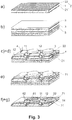
- the beam processing takes place in stage 11 and a further stage 12 (only in Fig. 3 , Step c) or d) drawn) in such a way that in the solder layer system 71 in the edge area 62 around the optically effective free-form surface 61 of the window element 6 a step 11 in the planar solder area of 50 ⁇ m-200 ⁇ m, which is slightly below the base area of the optical coating 2 is lowered deeper than the thickness of the optical coating 2, preferably up to twice the optical coating thickness, and a further step 12 in the range of 200 ⁇ m-500 ⁇ m is produced in the outer edge region 62.
- a step 11 in the planar solder area of 50 ⁇ m-200 ⁇ m which is slightly below the base area of the optical coating 2 is lowered deeper than the thickness of the optical coating 2, preferably up to twice the optical coating thickness, and a further step 12 in the range of 200 ⁇ m-500 ⁇ m is produced in the outer edge region 62.
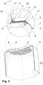
- the further step 12 which can also only be designed as a rounded edge 13 with a radius R between 50 and 150 ⁇ m (as in Fig. 5 shown), it is ensured that the metallization 7 is not only applied in a planar manner on the contact surface of the window element 6 to the housing 9, but also the edge of the window element 6 is coated with a solder layer 8 and thus notch cracking is minimized in the event of thermal or mechanical stress ( please refer Fig. 2 , Fig. 3 and especially the detail drawing in Fig. 5 ).
- the step 11 ensures a solder connection encompassing the edge of the housing for lowering the contact surface level below the base level of the optical coating 2 without reflection or scattered light or any other interfering light entering the filter layers of the optical coating 2 from the soldering layer 8.
- the step 11 of the carrier material removal down to below the base surface of the optical coating 2 contributes to the fact that the thickness of the protective layer 3, which should usually be three to five times the desired thickness of the overlying solder layer system 71, ensures sufficient stability for the lift.
- the protective layer 3 can be reduced to a thickness that is minimally greater than or equal to the thickness of the solder layer system 71.
- the roughness of the surface of the carrier material 1 is structured by the laser processing so that an enlarged surface is created which is available for the solder connection after the metallization 7 and thus contributes to improved system stability with regard to the hermetically sealed joining system. Due to the surface enlargement of the soldering contact surfaces produced by means of the roughness, but also by the rounded edge 13 and a beveled side surface 14, the so-called web width of the edge areas 62 of the window elements 6 from usually 500 ⁇ m to 800 ⁇ m to up to 100 ⁇ m can be achieved with improved system stability of the hermetic seal can be lowered, with an optimal range between 300 and 500 ⁇ m.
- the beveled side surfaces 14 of the window elements 6 are inclined towards the machined edge area 62 as a soldering contact surface (more clearly visible in the enlarged section of FIG Fig. 5 , with a bevel angle W of the outer edge between 1 ° and 15 ° relative to the surface normal of the solder contact surface being suitably selected, and bevel angles between 8 ° -12 ° are preferred.
- a housing 9, in which at least two window elements 2 of different shapes are inserted, is shown in a sectional view.
- the window elements 6 are quarter-shaped or semicircular free-form surfaces 62 with rounded corners.
- the optical coating 2 is applied only to the inside of the window element 6, without loss of generality.
- the metallization 7 and the solder layer 8 can only be seen. What is essential here is the formation of all edge transitions of the window element 6 as rounded edges 13, as a result of which the solder material of the soldering layer 8 clings to the solder ring structure of the window element in a stress-free and more durable manner.
- the thickness of the soldering layer 8 depends primarily on the selected roughness of the surface of the window element 6 removed as step 11 and is between 300 nm and 5 ⁇ m, preferably between 1 to 3 ⁇ m, the greater thicknesses with greater surface roughness (of up to 2.5 ⁇ m) are used.
- the laser coupling into the optical layers of the optical coating 2 can be initiated more easily. This can be supported by roughening by means of etching the Al layer (which should be> 100 nm and not larger than 5 ⁇ m) or thin absorbent layers made of Cr, Ti etc. (which have a layer thickness between 50 nm and 1 ⁇ m).
- Figures 7A-C show, for example, an anti-reflective coating (AR filter 21) for the range 3 - 11 ⁇ m on a Ge substrate ( Figure 7A ) or as an example of an optical coating 2, which is preferably on the Outside, but also alternatively on the inside of the window element 6, a long-pass filter for 8-12 ⁇ m on a Si substrate ( Figure 7B ) or a bandpass filter for 5.7 - 7 ⁇ m on a BaF2 substrate ( Figure 7C ).
- AR filter 21 anti-reflective coating
- Figure 7A an optical coating 2 for the range 3 - 11 ⁇ m on a Ge substrate
- an optical coating 2 which is preferably on the Outside, but also alternatively on the inside of the window element 6, a long-pass filter for 8-12 ⁇ m on a Si substrate ( Figure 7B ) or a bandpass filter for 5.7 - 7 ⁇ m on a BaF2 substrate ( Figure 7C ).
- an upper final layer can advantageously be applied, which is a silicon nitride, zinc sulfide or a DLC layer (diamond-like carbon layer) or a layer made of an oxide of silicon, magnesium, aluminum or a layer of a Fluoride of yttrium, ytterbium, barium or a semiconductor layer of germanium or silicon can be.
- the majority of the available optical coatings 2 (for example AR filters 21 and / or filter system 22) have either a transparent or reflective effect for the laser wavelength used here.
- the generated metallic protective layer 3 ensures process-stable absorption of the radiation energy in the material. This enables sublimation / ablation of the protective layer 3, the optical coating 2 and the carrier material 1.
- the metallic protective layer 3 is made of aluminum (Al), the Al being dissolved by NaOH with a low concentration (1 ... 5%).
- nickel or nickel alloys such as iron-nickel alloys, or also aluminum alloys, such as aluminum-silicon, aluminum-magnesium or aluminum-lithium alloys, can also be used as protective layer 3.
- the method can also be optimized in that after the partial ablative removal of the metallic protective layer 3 or the polymer protective layer (e.g. photoresist layer) and the optical coating 2, the optically effective free-form surface 61 is completely cut out and the window elements 6 previously partially in this way Holding substrate 5, as in Fig. 3 shown, have been fixed by selective gluing or pasting, so that in this variant they can be cleaned and coated with the solder layer system 71.
- the metallic protective layer 3 or the polymer protective layer e.g. photoresist layer
- the optically effective free-form surface 61 is completely cut out and the window elements 6 previously partially in this way Holding substrate 5, as in Fig. 3 shown, have been fixed by selective gluing or pasting, so that in this variant they can be cleaned and coated with the solder layer system 71.
- An optical coating 2 is used, the top layer of which is resistant to weak alkalis, which are used to etch back the protective layer 3.
- a silicon nitride, zinc sulfide or a DLC (Diamond.Like Carbon) layer is particularly suitable as a top layer.
Landscapes
- Physics & Mathematics (AREA)
- General Physics & Mathematics (AREA)
- Optics & Photonics (AREA)
- Spectroscopy & Molecular Physics (AREA)
- Chemical & Material Sciences (AREA)
- Crystallography & Structural Chemistry (AREA)
- Laser Beam Processing (AREA)
- Semiconductor Lasers (AREA)
- Mounting And Adjusting Of Optical Elements (AREA)
- Led Device Packages (AREA)
- Light Receiving Elements (AREA)
- Optical Couplings Of Light Guides (AREA)
Applications Claiming Priority (2)
| Application Number | Priority Date | Filing Date | Title |
|---|---|---|---|
| DE102013008478.4A DE102013008478A1 (de) | 2013-05-13 | 2013-05-13 | Verfahren zur Herstellung von in ein Gehäuse hermetisch dicht einlötbaren Fensterelementen und danach hergestellte Freiformfensterelemente |
| PCT/DE2014/100165 WO2014183746A1 (de) | 2013-05-13 | 2014-05-13 | Verfahren zur herstellung von in ein gehäuse hermetisch dicht einlötbaren fensterelementen und danach hergestellte freiformfensterelemente |
Publications (2)
| Publication Number | Publication Date |
|---|---|
| EP2997406A1 EP2997406A1 (de) | 2016-03-23 |
| EP2997406B1 true EP2997406B1 (de) | 2021-09-29 |
Family
ID=51211462
Family Applications (1)
| Application Number | Title | Priority Date | Filing Date |
|---|---|---|---|
| EP14741504.6A Active EP2997406B1 (de) | 2013-05-13 | 2014-05-13 | Verfahren zur herstellung von in ein gehäuse hermetisch dicht einlötbaren fensterelementen und danach hergestellte freiformfensterelemente |
Country Status (6)
| Country | Link |
|---|---|
| US (1) | US10330941B2 (enExample) |
| EP (1) | EP2997406B1 (enExample) |
| JP (1) | JP6388644B2 (enExample) |
| CN (1) | CN105209949B (enExample) |
| DE (2) | DE102013008478A1 (enExample) |
| WO (1) | WO2014183746A1 (enExample) |
Families Citing this family (8)
| Publication number | Priority date | Publication date | Assignee | Title |
|---|---|---|---|---|
| US9560781B2 (en) * | 2013-07-19 | 2017-01-31 | Materion Corporation | Metal cap assembly for optical communications |
| DE102017109913A1 (de) * | 2017-05-09 | 2018-11-15 | Henke-Sass, Wolf Gmbh | Linse für ein distales Ende eines Optikkanals eines Endoskopschaftes |
| DE112018004026A5 (de) * | 2017-08-07 | 2020-05-28 | Jenoptik Optical Systems Gmbh | Lagetoleranzunempfindliches kontaktierungsmodul zur kontaktierung optoelektronischer chips |
| CN109788643B (zh) * | 2017-11-10 | 2024-07-30 | 泰连公司 | 铝基可焊接的触头 |
| DE102018107697B4 (de) * | 2018-03-29 | 2020-12-10 | Hegla Boraident Gmbh & Co. Kg | Entschichtungseinrichtungen und -verfahren zum Entschichten von Glastafeln, vorzugsweise Verbundglastafeln |
| CN114895393B (zh) * | 2022-05-23 | 2023-09-05 | 无锡泓瑞航天科技有限公司 | 一种晶圆级金属化光学窗片及其制备方法 |
| CN115064599B (zh) * | 2022-06-10 | 2024-04-02 | 无锡泓瑞航天科技有限公司 | 一种红外探测器用金属化窗片的金属膜层制备方法 |
| CN118377099B (zh) * | 2024-03-15 | 2025-12-19 | 华侨大学 | 一种光学窗口的封装方法 |
Family Cites Families (14)
| Publication number | Priority date | Publication date | Assignee | Title |
|---|---|---|---|---|
| JPS51156770U (enExample) * | 1975-06-07 | 1976-12-14 | ||
| JPH07101721B2 (ja) * | 1988-06-03 | 1995-11-01 | 住友特殊金属株式会社 | 集積回路用Agろう付きシールリング及びその製造方法 |
| JPH06201454A (ja) * | 1992-12-30 | 1994-07-19 | Horiba Ltd | 赤外線検出器 |
| JPH0799368A (ja) * | 1993-09-29 | 1995-04-11 | Mitsubishi Electric Corp | 光半導体装置 |
| US5882988A (en) * | 1995-08-16 | 1999-03-16 | Philips Electronics North America Corporation | Semiconductor chip-making without scribing |
| JPH11211555A (ja) * | 1998-01-29 | 1999-08-06 | Horiba Ltd | 赤外線検出器 |
| US6962834B2 (en) * | 2002-03-22 | 2005-11-08 | Stark David H | Wafer-level hermetic micro-device packages |
| DE102004049134A1 (de) * | 2004-10-07 | 2006-04-13 | Schott Ag | Metallreflektor und Verfahren zu dessen Herstellung |
| DE102005024512B3 (de) | 2005-05-26 | 2007-02-08 | Jenoptik Laser, Optik, Systeme Gmbh | Verfahren zur Herstellung von in ein Gehäuse hermetisch dicht einlötbaren Fensterelementen |
| DE102007039291A1 (de) * | 2007-08-20 | 2009-02-26 | Osram Opto Semiconductors Gmbh | Optoelektronisches Halbleitermodul und Verfahren zur Herstellung eines solchen |
| JP2009276691A (ja) * | 2008-05-16 | 2009-11-26 | Nippon Shinku Kogaku Kk | 光学素子及びその製造方法 |
| JP2010045117A (ja) * | 2008-08-11 | 2010-02-25 | Disco Abrasive Syst Ltd | 光デバイスウエーハの加工方法 |
| JP5492213B2 (ja) * | 2009-08-17 | 2014-05-14 | パナソニック株式会社 | 赤外線センサ |
| US20140093688A1 (en) * | 2012-09-28 | 2014-04-03 | Yindar Chuo | Method for fabrication of nano-structures |
-
2013
- 2013-05-13 DE DE102013008478.4A patent/DE102013008478A1/de not_active Withdrawn
-
2014
- 2014-05-13 WO PCT/DE2014/100165 patent/WO2014183746A1/de not_active Ceased
- 2014-05-13 JP JP2016513228A patent/JP6388644B2/ja active Active
- 2014-05-13 DE DE112014002384.1T patent/DE112014002384A5/de not_active Withdrawn
- 2014-05-13 EP EP14741504.6A patent/EP2997406B1/de active Active
- 2014-05-13 CN CN201480027085.0A patent/CN105209949B/zh active Active
-
2015
- 2015-11-12 US US14/939,385 patent/US10330941B2/en active Active
Also Published As
| Publication number | Publication date |
|---|---|
| US20160062127A1 (en) | 2016-03-03 |
| EP2997406A1 (de) | 2016-03-23 |
| US10330941B2 (en) | 2019-06-25 |
| JP6388644B2 (ja) | 2018-09-12 |
| DE112014002384A5 (de) | 2016-07-14 |
| CN105209949B (zh) | 2018-08-24 |
| CN105209949A (zh) | 2015-12-30 |
| JP2016526290A (ja) | 2016-09-01 |
| WO2014183746A1 (de) | 2014-11-20 |
| WO2014183746A4 (de) | 2015-01-29 |
| DE102013008478A1 (de) | 2014-11-13 |
Similar Documents
| Publication | Publication Date | Title |
|---|---|---|
| EP2997406B1 (de) | Verfahren zur herstellung von in ein gehäuse hermetisch dicht einlötbaren fensterelementen und danach hergestellte freiformfensterelemente | |
| DE10164494B4 (de) | Verkapseltes Bauelement mit geringer Bauhöhe sowie Verfahren zur Herstellung | |
| DE102007051823B4 (de) | Sensor für eine physikalische Grösse und Verfahren zur Fertigung des Sensors | |
| DE102008005686B9 (de) | MEMS-Bauelement und Verfahren zur Herstellung eines MEMS-Bauelements | |
| WO2012136544A1 (de) | Waferlevel-package und verfahren zur herstellung | |
| DE10164502A1 (de) | Verfahren zur hermetischen Verkapselung eines Bauelements | |
| EP2041787A1 (de) | Verfahren zur verkapselung elektronischer bauelemente und integrierter schaltungen | |
| EP1866236A1 (de) | Mikromechanisches bauteil sowie verfahren zur herstellung eines mikromechanischen bauteils | |
| EP1869705B1 (de) | Verfahren zur herstellung gehäuster elektronischer bauelemente und gehäustes elektronisches bauelement | |
| DE10055081A1 (de) | Mikrostrukturbauelement | |
| EP3682474B1 (de) | Verbund aus mehreren adapterelementen und verfahren zur herstellung eines solchen verbunds | |
| EP4311819A1 (de) | Metall-keramik-substrat mit kontaktbereich | |
| US7468293B2 (en) | Method for the production of window elements which can be soldered into a housing in a hermetically tight manner and of a window element sealing a housing | |
| EP1111671A2 (de) | Verfahren zum Herstellen einer Halbleiteranordnung | |
| DE10350707A1 (de) | Elektrischer Kontakt für optoelektronischen Halbleiterchip und Verfahren zu dessen Herstellung | |
| DE112019006574T5 (de) | Strukturkörper, strukturkörperherstellungsverfahren und elektronisches gerät | |
| JPH11177186A (ja) | オプトエレクトロニック・アセンブリの製造における腐食の防止 | |
| DE102019219641A1 (de) | Verfahren zur Herstellung einer mikromechanischen Vorrichtung mittels eutektischem Bonden und mikromechanische Vorrichtung | |
| DE102015101878A1 (de) | Mit Aktivlot versiegelte Mikrosystemtechnik-Bauelemente, Komponenten hierfür und Lottransferverfahren zu ihrer Herstellung | |
| EP4037865B1 (de) | Verfahren zum bearbeiten und befestigen eines metall-keramik-substrate | |
| EP4663620A1 (de) | Verfahren zur herstellung eines metall-keramik-substrats und metall-keramik-substrat | |
| DE102015122434A1 (de) | MEMS Bauelement | |
| WO2024022743A1 (de) | Metall-keramik-substrat mit kontaktbereich | |
| DE102020205190A1 (de) | Herstellungsverfahren zum Herstellen zumindest einer Kappenvorrichtung oder eines Kappenwafers | |
| DE102009046461A1 (de) | Verfahren zur Herstellung verkappter mikroelektromechanischer Bauelemente |
Legal Events
| Date | Code | Title | Description |
|---|---|---|---|
| PUAI | Public reference made under article 153(3) epc to a published international application that has entered the european phase |
Free format text: ORIGINAL CODE: 0009012 |
|
| 17P | Request for examination filed |
Effective date: 20151211 |
|
| AK | Designated contracting states |
Kind code of ref document: A1 Designated state(s): AL AT BE BG CH CY CZ DE DK EE ES FI FR GB GR HR HU IE IS IT LI LT LU LV MC MK MT NL NO PL PT RO RS SE SI SK SM TR |
|
| AX | Request for extension of the european patent |
Extension state: BA ME |
|
| 17Q | First examination report despatched |
Effective date: 20160418 |
|
| DAX | Request for extension of the european patent (deleted) | ||
| STAA | Information on the status of an ep patent application or granted ep patent |
Free format text: STATUS: EXAMINATION IS IN PROGRESS |
|
| GRAP | Despatch of communication of intention to grant a patent |
Free format text: ORIGINAL CODE: EPIDOSNIGR1 |
|
| STAA | Information on the status of an ep patent application or granted ep patent |
Free format text: STATUS: GRANT OF PATENT IS INTENDED |
|
| RIC1 | Information provided on ipc code assigned before grant |
Ipc: H01L 31/0232 20140101ALI20210322BHEP Ipc: G01J 5/04 20060101ALI20210322BHEP Ipc: G01J 1/02 20060101ALI20210322BHEP Ipc: G01J 5/08 20060101ALI20210322BHEP Ipc: G02B 1/02 20060101ALI20210322BHEP Ipc: G02B 7/00 20210101AFI20210322BHEP |
|
| INTG | Intention to grant announced |
Effective date: 20210428 |
|
| GRAS | Grant fee paid |
Free format text: ORIGINAL CODE: EPIDOSNIGR3 |
|
| GRAA | (expected) grant |
Free format text: ORIGINAL CODE: 0009210 |
|
| STAA | Information on the status of an ep patent application or granted ep patent |
Free format text: STATUS: THE PATENT HAS BEEN GRANTED |
|
| AK | Designated contracting states |
Kind code of ref document: B1 Designated state(s): AL AT BE BG CH CY CZ DE DK EE ES FI FR GB GR HR HU IE IS IT LI LT LU LV MC MK MT NL NO PL PT RO RS SE SI SK SM TR |
|
| REG | Reference to a national code |
Ref country code: GB Ref legal event code: FG4D Free format text: NOT ENGLISH |
|
| REG | Reference to a national code |
Ref country code: CH Ref legal event code: EP Ref country code: AT Ref legal event code: REF Ref document number: 1434703 Country of ref document: AT Kind code of ref document: T Effective date: 20211015 |
|
| REG | Reference to a national code |
Ref country code: DE Ref legal event code: R096 Ref document number: 502014015906 Country of ref document: DE |
|
| REG | Reference to a national code |
Ref country code: IE Ref legal event code: FG4D Free format text: LANGUAGE OF EP DOCUMENT: GERMAN |
|
| REG | Reference to a national code |
Ref country code: LT Ref legal event code: MG9D |
|
| REG | Reference to a national code |
Ref country code: SE Ref legal event code: TRGR |
|
| PG25 | Lapsed in a contracting state [announced via postgrant information from national office to epo] |
Ref country code: HR Free format text: LAPSE BECAUSE OF FAILURE TO SUBMIT A TRANSLATION OF THE DESCRIPTION OR TO PAY THE FEE WITHIN THE PRESCRIBED TIME-LIMIT Effective date: 20210929 Ref country code: RS Free format text: LAPSE BECAUSE OF FAILURE TO SUBMIT A TRANSLATION OF THE DESCRIPTION OR TO PAY THE FEE WITHIN THE PRESCRIBED TIME-LIMIT Effective date: 20210929 Ref country code: NO Free format text: LAPSE BECAUSE OF FAILURE TO SUBMIT A TRANSLATION OF THE DESCRIPTION OR TO PAY THE FEE WITHIN THE PRESCRIBED TIME-LIMIT Effective date: 20211229 Ref country code: FI Free format text: LAPSE BECAUSE OF FAILURE TO SUBMIT A TRANSLATION OF THE DESCRIPTION OR TO PAY THE FEE WITHIN THE PRESCRIBED TIME-LIMIT Effective date: 20210929 Ref country code: BG Free format text: LAPSE BECAUSE OF FAILURE TO SUBMIT A TRANSLATION OF THE DESCRIPTION OR TO PAY THE FEE WITHIN THE PRESCRIBED TIME-LIMIT Effective date: 20211229 Ref country code: LT Free format text: LAPSE BECAUSE OF FAILURE TO SUBMIT A TRANSLATION OF THE DESCRIPTION OR TO PAY THE FEE WITHIN THE PRESCRIBED TIME-LIMIT Effective date: 20210929 |
|
| REG | Reference to a national code |
Ref country code: NL Ref legal event code: MP Effective date: 20210929 |
|
| PG25 | Lapsed in a contracting state [announced via postgrant information from national office to epo] |
Ref country code: LV Free format text: LAPSE BECAUSE OF FAILURE TO SUBMIT A TRANSLATION OF THE DESCRIPTION OR TO PAY THE FEE WITHIN THE PRESCRIBED TIME-LIMIT Effective date: 20210929 Ref country code: GR Free format text: LAPSE BECAUSE OF FAILURE TO SUBMIT A TRANSLATION OF THE DESCRIPTION OR TO PAY THE FEE WITHIN THE PRESCRIBED TIME-LIMIT Effective date: 20211230 |
|
| PG25 | Lapsed in a contracting state [announced via postgrant information from national office to epo] |
Ref country code: IS Free format text: LAPSE BECAUSE OF FAILURE TO SUBMIT A TRANSLATION OF THE DESCRIPTION OR TO PAY THE FEE WITHIN THE PRESCRIBED TIME-LIMIT Effective date: 20220129 Ref country code: SK Free format text: LAPSE BECAUSE OF FAILURE TO SUBMIT A TRANSLATION OF THE DESCRIPTION OR TO PAY THE FEE WITHIN THE PRESCRIBED TIME-LIMIT Effective date: 20210929 Ref country code: RO Free format text: LAPSE BECAUSE OF FAILURE TO SUBMIT A TRANSLATION OF THE DESCRIPTION OR TO PAY THE FEE WITHIN THE PRESCRIBED TIME-LIMIT Effective date: 20210929 Ref country code: PT Free format text: LAPSE BECAUSE OF FAILURE TO SUBMIT A TRANSLATION OF THE DESCRIPTION OR TO PAY THE FEE WITHIN THE PRESCRIBED TIME-LIMIT Effective date: 20220131 Ref country code: PL Free format text: LAPSE BECAUSE OF FAILURE TO SUBMIT A TRANSLATION OF THE DESCRIPTION OR TO PAY THE FEE WITHIN THE PRESCRIBED TIME-LIMIT Effective date: 20210929 Ref country code: NL Free format text: LAPSE BECAUSE OF FAILURE TO SUBMIT A TRANSLATION OF THE DESCRIPTION OR TO PAY THE FEE WITHIN THE PRESCRIBED TIME-LIMIT Effective date: 20210929 Ref country code: ES Free format text: LAPSE BECAUSE OF FAILURE TO SUBMIT A TRANSLATION OF THE DESCRIPTION OR TO PAY THE FEE WITHIN THE PRESCRIBED TIME-LIMIT Effective date: 20210929 Ref country code: EE Free format text: LAPSE BECAUSE OF FAILURE TO SUBMIT A TRANSLATION OF THE DESCRIPTION OR TO PAY THE FEE WITHIN THE PRESCRIBED TIME-LIMIT Effective date: 20210929 Ref country code: CZ Free format text: LAPSE BECAUSE OF FAILURE TO SUBMIT A TRANSLATION OF THE DESCRIPTION OR TO PAY THE FEE WITHIN THE PRESCRIBED TIME-LIMIT Effective date: 20210929 Ref country code: AL Free format text: LAPSE BECAUSE OF FAILURE TO SUBMIT A TRANSLATION OF THE DESCRIPTION OR TO PAY THE FEE WITHIN THE PRESCRIBED TIME-LIMIT Effective date: 20210929 |
|
| REG | Reference to a national code |
Ref country code: DE Ref legal event code: R097 Ref document number: 502014015906 Country of ref document: DE |
|
| PG25 | Lapsed in a contracting state [announced via postgrant information from national office to epo] |
Ref country code: DK Free format text: LAPSE BECAUSE OF FAILURE TO SUBMIT A TRANSLATION OF THE DESCRIPTION OR TO PAY THE FEE WITHIN THE PRESCRIBED TIME-LIMIT Effective date: 20210929 |
|
| PLBE | No opposition filed within time limit |
Free format text: ORIGINAL CODE: 0009261 |
|
| STAA | Information on the status of an ep patent application or granted ep patent |
Free format text: STATUS: NO OPPOSITION FILED WITHIN TIME LIMIT |
|
| 26N | No opposition filed |
Effective date: 20220630 |
|
| PG25 | Lapsed in a contracting state [announced via postgrant information from national office to epo] |
Ref country code: SI Free format text: LAPSE BECAUSE OF FAILURE TO SUBMIT A TRANSLATION OF THE DESCRIPTION OR TO PAY THE FEE WITHIN THE PRESCRIBED TIME-LIMIT Effective date: 20210929 |
|
| REG | Reference to a national code |
Ref country code: CH Ref legal event code: PL |
|
| REG | Reference to a national code |
Ref country code: BE Ref legal event code: MM Effective date: 20220531 |
|
| PG25 | Lapsed in a contracting state [announced via postgrant information from national office to epo] |
Ref country code: MC Free format text: LAPSE BECAUSE OF FAILURE TO SUBMIT A TRANSLATION OF THE DESCRIPTION OR TO PAY THE FEE WITHIN THE PRESCRIBED TIME-LIMIT Effective date: 20210929 Ref country code: LU Free format text: LAPSE BECAUSE OF NON-PAYMENT OF DUE FEES Effective date: 20220513 Ref country code: LI Free format text: LAPSE BECAUSE OF NON-PAYMENT OF DUE FEES Effective date: 20220531 Ref country code: IT Free format text: LAPSE BECAUSE OF FAILURE TO SUBMIT A TRANSLATION OF THE DESCRIPTION OR TO PAY THE FEE WITHIN THE PRESCRIBED TIME-LIMIT Effective date: 20210929 Ref country code: CH Free format text: LAPSE BECAUSE OF NON-PAYMENT OF DUE FEES Effective date: 20220531 |
|
| PG25 | Lapsed in a contracting state [announced via postgrant information from national office to epo] |
Ref country code: IE Free format text: LAPSE BECAUSE OF NON-PAYMENT OF DUE FEES Effective date: 20220513 Ref country code: FR Free format text: LAPSE BECAUSE OF NON-PAYMENT OF DUE FEES Effective date: 20220531 |
|
| PG25 | Lapsed in a contracting state [announced via postgrant information from national office to epo] |
Ref country code: BE Free format text: LAPSE BECAUSE OF NON-PAYMENT OF DUE FEES Effective date: 20220531 |
|
| REG | Reference to a national code |
Ref country code: AT Ref legal event code: MM01 Ref document number: 1434703 Country of ref document: AT Kind code of ref document: T Effective date: 20220513 |
|
| PG25 | Lapsed in a contracting state [announced via postgrant information from national office to epo] |
Ref country code: AT Free format text: LAPSE BECAUSE OF NON-PAYMENT OF DUE FEES Effective date: 20220513 |
|
| REG | Reference to a national code |
Ref country code: DE Ref legal event code: R082 Ref document number: 502014015906 Country of ref document: DE Representative=s name: GLEIM PETRI PATENT- UND RECHTSANWALTSPARTNERSC, DE |
|
| PG25 | Lapsed in a contracting state [announced via postgrant information from national office to epo] |
Ref country code: HU Free format text: LAPSE BECAUSE OF FAILURE TO SUBMIT A TRANSLATION OF THE DESCRIPTION OR TO PAY THE FEE WITHIN THE PRESCRIBED TIME-LIMIT; INVALID AB INITIO Effective date: 20140513 |
|
| PG25 | Lapsed in a contracting state [announced via postgrant information from national office to epo] |
Ref country code: SM Free format text: LAPSE BECAUSE OF FAILURE TO SUBMIT A TRANSLATION OF THE DESCRIPTION OR TO PAY THE FEE WITHIN THE PRESCRIBED TIME-LIMIT Effective date: 20210929 Ref country code: MK Free format text: LAPSE BECAUSE OF FAILURE TO SUBMIT A TRANSLATION OF THE DESCRIPTION OR TO PAY THE FEE WITHIN THE PRESCRIBED TIME-LIMIT Effective date: 20210929 Ref country code: CY Free format text: LAPSE BECAUSE OF FAILURE TO SUBMIT A TRANSLATION OF THE DESCRIPTION OR TO PAY THE FEE WITHIN THE PRESCRIBED TIME-LIMIT Effective date: 20210929 |
|
| PG25 | Lapsed in a contracting state [announced via postgrant information from national office to epo] |
Ref country code: MT Free format text: LAPSE BECAUSE OF FAILURE TO SUBMIT A TRANSLATION OF THE DESCRIPTION OR TO PAY THE FEE WITHIN THE PRESCRIBED TIME-LIMIT Effective date: 20210929 |
|
| PGFP | Annual fee paid to national office [announced via postgrant information from national office to epo] |
Ref country code: DE Payment date: 20250519 Year of fee payment: 12 |
|
| PGFP | Annual fee paid to national office [announced via postgrant information from national office to epo] |
Ref country code: GB Payment date: 20250522 Year of fee payment: 12 |
|
| PGFP | Annual fee paid to national office [announced via postgrant information from national office to epo] |
Ref country code: SE Payment date: 20250522 Year of fee payment: 12 |
|
| PG25 | Lapsed in a contracting state [announced via postgrant information from national office to epo] |
Ref country code: TR Free format text: LAPSE BECAUSE OF FAILURE TO SUBMIT A TRANSLATION OF THE DESCRIPTION OR TO PAY THE FEE WITHIN THE PRESCRIBED TIME-LIMIT Effective date: 20210929 |