EP2972598B1 - Mixed signal tdc with embedded t2v adc - Google Patents
Mixed signal tdc with embedded t2v adc Download PDFInfo
- Publication number
- EP2972598B1 EP2972598B1 EP14714891.0A EP14714891A EP2972598B1 EP 2972598 B1 EP2972598 B1 EP 2972598B1 EP 14714891 A EP14714891 A EP 14714891A EP 2972598 B1 EP2972598 B1 EP 2972598B1
- Authority
- EP
- European Patent Office
- Prior art keywords
- signal
- time
- voltage
- supply voltage
- digital converter
- Prior art date
- Legal status (The legal status is an assumption and is not a legal conclusion. Google has not performed a legal analysis and makes no representation as to the accuracy of the status listed.)
- Not-in-force
Links
Images





Classifications
-
- H—ELECTRICITY
- H03—ELECTRONIC CIRCUITRY
- H03M—CODING; DECODING; CODE CONVERSION IN GENERAL
- H03M1/00—Analogue/digital conversion; Digital/analogue conversion
- H03M1/12—Analogue/digital converters
- H03M1/50—Analogue/digital converters with intermediate conversion to time interval
-
- G—PHYSICS
- G04—HOROLOGY
- G04F—TIME-INTERVAL MEASURING
- G04F10/00—Apparatus for measuring unknown time intervals by electric means
- G04F10/005—Time-to-digital converters [TDC]
-
- H—ELECTRICITY
- H03—ELECTRONIC CIRCUITRY
- H03L—AUTOMATIC CONTROL, STARTING, SYNCHRONISATION OR STABILISATION OF GENERATORS OF ELECTRONIC OSCILLATIONS OR PULSES
- H03L7/00—Automatic control of frequency or phase; Synchronisation
- H03L7/06—Automatic control of frequency or phase; Synchronisation using a reference signal applied to a frequency- or phase-locked loop
- H03L7/08—Details of the phase-locked loop
-
- H—ELECTRICITY
- H03—ELECTRONIC CIRCUITRY
- H03L—AUTOMATIC CONTROL, STARTING, SYNCHRONISATION OR STABILISATION OF GENERATORS OF ELECTRONIC OSCILLATIONS OR PULSES
- H03L7/00—Automatic control of frequency or phase; Synchronisation
- H03L7/06—Automatic control of frequency or phase; Synchronisation using a reference signal applied to a frequency- or phase-locked loop
- H03L7/08—Details of the phase-locked loop
- H03L7/099—Details of the phase-locked loop concerning mainly the controlled oscillator of the loop
- H03L7/0991—Details of the phase-locked loop concerning mainly the controlled oscillator of the loop the oscillator being a digital oscillator, e.g. composed of a fixed oscillator followed by a variable frequency divider
-
- H—ELECTRICITY
- H03—ELECTRONIC CIRCUITRY
- H03L—AUTOMATIC CONTROL, STARTING, SYNCHRONISATION OR STABILISATION OF GENERATORS OF ELECTRONIC OSCILLATIONS OR PULSES
- H03L2207/00—Indexing scheme relating to automatic control of frequency or phase and to synchronisation
- H03L2207/50—All digital phase-locked loop
Definitions
- the present disclosure relates to electronic circuits, and more particualry to a time-to-digital converter.
- a time-to-digital converter is an electronic circuit that converts the difference between transition times of two signals to a digital signal whose value is proportional to such timing difference.
- a time-to-digital converter may be used in a phase-locked loop to convert the difference between the transition times of a reference clock signal and an oscillating signal to a digital signal in order to lock the phase of the oscillating signal to the phase of the clock signal.
- US 2008/169826 A1 discloses a time-to-digital converter comprising:
- a time-to-digital converter according to the present invention is defined in independent claim 1. Preferred embodiments are defined in the dependent claims 2-8.
- FIG. 1 is a block diagram of a time-to-digital converter (TDC) 50, in accordance with one exemplary embodiment of the present invention.
- TDC 50 is shown as including, in part, an edge detector 100, a time-to-voltage converter (T2V) 150, and an analog-to-digital converter (ADC) 300.
- edge detector 100 an edge detector 100
- T2V time-to-voltage converter
- ADC analog-to-digital converter
- Edge detector 100 is adapted to receive an oscillating signal DCO 10, and a reference clock signal FREF 12 that has a longer time period than signal DCO 10. Accordingly, during each period of signal FREF 12, a number of transitions (edges) occur on signal DCO 10. In one embodiment, during each period of signal FREF 12, edge detector 100 filters out all DCO 10 signal edges except the rising (or falling) DCO 10 edge that is closest in time to the rising (or falling) edge of signal FREF 12 in that period. The DCO 10 signal edge detected as being closest in time to the rising (or falling) edge of signal FREF 12 is supplied as output signal CKV 14. The corresponding edge of signal FREF 12 is supplied as output signal REF 16 by edge detector 100.
- edge detector 100 may detect the second closest DCO 10 edge to the FREF 12 signal edge. In yet other embodiments, during each period, edge detector 100 detects the DCO 10 edge satisfying a predefined relationship to the FREF 12 edge. The detected DCO 10 edge in all such embodiments is supplied as output signal CKV 14.
- T2V converter 150 is adapted to generate a voltage proportional to the difference in transition times (edges) of signals CKV 14 and REF 16. Accordingly, the longer is the time difference (delay) between transitions of signals CKV 14 and REF 16, the greater is the differential voltage generated across output nodes OUT 18 and OUT_B 20 of T2V converter 150.
- Signal RESET 26 is used to charge the voltage of output nodes OUT 18 and OUT B 20 to predefined voltage levels, as is described further below.
- ADC 300 is adapted to convert the differential voltage it receives from output nodes OUT 18, OUT_B 20 to a pair of differential N-bit digital signals B[1:N] 22 and BB[1:N] 24.
- ADC 300 may be a successive approximation register (SAR) ADC.
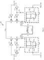
- FIG. 2A is a schematic diagram of a TDC 75 having disposed therein a T2V converter 200, in accordance with one exemplary embodiment of the present invention.
- T2V 200 which is one embodiment of T2V 150 of Figure 1 , is shown as including transistors 202, 204, 206, 212, 214, 216, capacitors 220, 222, as well inverters 208 and 218.
- Figure 2B is a timing diagram of a number of signals associated with T2V converter 200 of Fig. 2A .
- signal RESET 26 resets output nodes OUT 18 and OUT B 20 to supply voltage VDD via PMOS transistors 202 and 212, respectively.
- Capacitors 220, 222 retain the charges stored at nodes OUT 18, OUT_B 20.
- signal RESET 26 is shown as being low, thereby causing nodes OUT 18 and OUT B 20 to be reset to supply voltage VDD.
- the drop in voltage level of node OUT_B 20 from VDD to V1 is dependent on the period (T2-T1). In other words, the longer the delay between the arrival of corresponding edges of signals REF and CKV, the greater is the drop in the voltage level of node OUT_B.
- the drop in voltage level of node OUT 18 from VDD to V2 is dependent on the period (T5-T4). In other words, the longer is the delay between arrival times of the corresponding edges (i.e., transition times) of signals REF 16 and CKV 14, the greater is the drop in the voltage level of node OUT 18.
- the differential voltage across nodes OUT 18 and OUT B 20 is converted to a digital signal by an analog-to-digital converter whose output voltage represents the output of the TDC.
- FIG 3 is a schematic diagram of a T2V converter 225, in accordance with another exemplary embodiment of the present invention.
- T2V 225 which is one embodiment of T2V 150 of Figure 1 , is shown as including transistors 238, 240, 242, 258, 260, 262, inverters 230, 232, 234, 250, 252, 254 and capacitors 236, 256.
- T2V 225 operates in the same manner as T2V converter 200 except that in T2V converter 225, NMOS transistors 242 and 262 cause output nodes OUT 18 and OUT_B 20 to be charged to reference voltage Vref in response to reset signal RESET 16.
- transistors 240, 258 are tuned on to form a conductive path from node OUT 18 to supply voltage Vchg, or conversely, transistors 260, 238 are tuned on to form a conductive path from node OUT B 20 to supply voltage Vchg.
- the voltage of one of the nodes OUT 18 or OUT_B 20 is enable to increase from Vref, while the voltage of the other node remains at Vref.
- the magnitude of this voltage increase is dependent on the difference between the arrival times of the corresponding edges of signals CKV 14 and REF 16.
- transistors 240, 258 turn on to form a conductive path between node OUT 18 and supply voltage Vchg. Accordingly, the voltage of node OUT 18 is enabled to increase.
- the increase in the voltage level of node OUT 18 is dependent on the period defined by the difference in the arrival times of the rising edges of signal CKV 14 and REF 16. The greater this difference, the higher is the voltage increase at node OUT 18. Because transistors 260 and 238 remain off during this period, the voltage at node OUT B 20 remains at voltage Vref.
- the difference in voltages of nodes OUT 18 and OUT B 20 is converted to a digital signal representing the output voltage of the TDC. In one embodiment, Vref is the ground potential.
- node OUT B 20 is enabled to increase.
- the increase in the voltage level of node OUT B 20 is dependent on the period defined by the difference in the arrival times of the rising edges of signal CKV 14 and REF 16. The greater this difference, the higher is the voltage increase at node OUT B 20. Because transistors 240 and 258 remain off during such a period, the voltage at node OUT 18 remains at voltage Vref. The difference in voltages of nodes OUT 18 and OUT B 20 is converted to a digital signal representing the output voltage of the TDC.
- FIG 4 is a schematic diagram of a T2V converter 250, in accordance with another exemplary embodiment of the present invention.
- T2V converter 250 which is one embodiment of T2V 150 of Figure 1 , is similar to T2V converter 225 except that T2V converter 250 includes first and second capacitor banks 280, 290 in place of capacitors 244, 264.
- Capacitor banks 280 and 290 are parts of a successive approximation register (SAR) ADC. Accordingly, in such embodiments the capacitor banks of the ADC are integrated within the T2V circuitry.
- SAR successive approximation register
- Capacitor bank 280 includes N capacitors 282 i and N switches 284 i , where i is an integer varying from 1 to N.
- a first terminal of each capacitor 282 i is coupled to node OUT 18.
- a second terminal of each capacitor 282 i is coupled to supply voltage Vref via an associated switch 284 i which opens or closes in response to one of the N bits of signal PhiP.
- the second terminal of capacitor 282 i receives voltage Vref when bit i of N-bit signal PhiP is asserted in order to close an associated switch 284 i .
- capacitor bank 290 includes N capacitors 292 i and N switches 294 i .
- a first terminal of each capacitor 292 i is coupled to node OUT_B 20.
- a second terminal of each capacitor 292 i is coupled to supply voltage Vref via an associated switch 294 i which opens or closes in response to one of the N bits of signal PhiN.
- the second terminal of capacitor 292 i receives Vref when bit i of N-bit signal PhiN is asserted in order to close an associated switch 294 i .
- the differential voltage across output nodes OUT 18, OUT B 20 of capacitor banks 280, 290 is converted to a digital signal using an ADC.
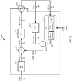
- FIG. 5 is a simplified block diagram of ADC 300 of Figure 1 , in accordance with one exemplary embodiment of the present invention.
- ADC 300 of Figure 5 is shown as being a SAR ADC, it is understood that ADC 300 may be any ADC.
- ADC 300 is adapted to convert the differential voltage supplied across nodes OUT 18, OUT B 20 to an N-bit digital signal.
- ADC 300 is shown as including comparator 310, control logic 320, and capacitor banks 280, 290, described above in reference to Figure 4 .
- Capacitors 282 i and 292 i of capacitor banks 280, 290 sample the voltages of nodes OUT 18, OUT B 20, and hold these voltages for comparison by comparator 310.
- the output of comparator 310 is a rail-to-rail differential voltage supplied across the comparator's output terminals P, N.
- Control logic 320 is adapted to digitize the differential voltage appearing across output terminals P, N of comparator 310 to generate a pair of N-bit differential signals B[1:N] and BB[1:N] representing the output of the TDC.
- Differential signals PhiP[1:N] and PhiN[1:N] controlling switches 284 i and 294 i of capacitors banks 280, 290 are also generated by control logic 320.
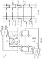
- Figures 6A and 7A together are a schematic diagram of edge detector 100 of Figure 1 , in accordance with one embodiment of the present invention.
- Figure 6A is a schematic diagram of an adjustable delay chain 450 adapted to generate a multitude of phases of clock signal Fref 12.
- Figure 7A is a block diagram of a logic circuit 500 adapted to generate signals CKV 14 and REF 16.
- delay chain 450 is shown as including a delay-locked loop 440, a multitude of buffers 404, 406, 408, 410, 412, 414, and a multitude of variable capacitors 424, 426, 428, 430, 432, 434 disposed between the buffers.
- the capacitances of the variable capacitors may be varied using delay-locked loop 440 such that the delay across any of the buffers having variable capacitors at its input and output terminals is one-quarter of the period of signal DCO 10. Accordingly, the delay across buffers 406, 408, 410, 412, and 414 is one-quarter of the period of signal DCO 10.
- Figure 6B is a timing diagram of signal Fref 12 and each of the delay signals Fref dl 42, Fref_d2 44, Fref_d3 46, Fref_d4 48, Fref_d5 50, and Fref_d6 52 generated by delay chain 450. As is seen, the delay across each buffer is one-quarter of the period of signal DCO 10.
- logic circuit 500 includes flip-flops 502, 506, 512, 514, inverter 504, and OR gate 508. During each period of signal FREF 12, logic circuit 500 filters out all transition (edges) of signal DCO 10 except the DCO 10 edge detected as being closest in time to the transition of signal FREF 12. The DCO 10 edge so detected is supplied as output signal CKV 14. The corresponding edge of signal FREF 12 is supplied as output signal REF 16.
- Signals Fref_d2 44 and DCO 10 are respectively applied to the clock and data input terminals of flip-flop 502. Assume signal DCO 10 leads signal Fref_d2 44, as shown in Figure 7B . Accordingly, on the rising edge of signal Fref_d2 44, the output signal of flip-flop 502, namely signal SYNC_CKV 54, makes a low-to-high transition (i.e., goes high), in turn causing the output of OR gate 508, namely signal EN 58 to go high. Because signals EN 58 and DCO 10 are respectively applied to the data and clock input terminals of flip-flop 512, on the next rising edge of signal DCO 10, signal CKV 14 goes high.
- signals VDD and Fref_d6 52 are respectively applied to the data and clock input terminals of flip-flop 514, on the next rising edge of signal Fref_d6 52, signal REF 16 goes high. Moreover, because signals Fref_d2 44and Fref_d6 52 are one DCO 10 period apart, signal REF 16 is asserted after substantially one period of signal DCO 10.
- Signal SYNC_CKVB 56 is the inverse of signal SYNC_CKV 54. Accordingly, when signal SYNC_CKV 54 is high, on the next rising edge of signal Fref_d5 50, output Q of flip-flop 506 goes low. Subsequently, when signal SYNC_CKV 54 goes low, signal EN also goes low until the next transition of signl Fref_d5 50 is received.
- Figure 7B is a timing diagram of a number of signals associated with logic block 500 when signal DCO 10 is assumed to lead signal Fref_d2 44 n phase.
- Signals DCO 10 and Fref_d2 44 are shown as being asserted respectively at times T1 and T2, with T1 occurring prior T2.
- Signals SYNC_CKV 54 and EN 58 are asserted at times T3, and T4, reflecting the delays across flip-flop 502 and OR logic 508.
- the next rising edge of signal DCO 10 occurs at time T5.
- signals CKV 14 and REF 16 are asserted reflecting the delays across flip-flops 510, and 512.
- Figure 7C is a timing diagram of a number of signals associated with logic circuit 500 when signal CKV 14 is assumed to lag signal Fref_d244 in phase.
- DCO 10 is assumed to go low.
- Fref_d2 44 is asserted, thereby causing signal SYNC CKVB 56 to go high at T3.
- T4 signal DCO 10 is shown as going high.
- T6 which is 3/4 of the period of signal DCO 10 after time T2
- signal Fref_d5 50 goes high, thereby causing signal EN 58 to go high at T6.
- FIG 8 is a block diagram of a digital phase-locked loop (PLL) 600 embodying a TDC, in accordance with one embodiment of the present invention.
- Digitally-controlled oscillator 608 generates a DCO 10 signal having a multitude of transitions during each period of reference clock signal FREF 12.
- TDC 50 is adapted to detect the DCO 10 edge that is closest in time to the edge of sinal FREF 12, and to generate in response a differential signal B 62 whose value is proportional to the timing difference between these two edges.
- Accumulator 612 is adapted to increment the DCO 10 value by one with each cycle of the clock thereby to generate a signal DCO_INC 64.
- Adder 610 sums the output values of TDC 50 and accumulator 612 to generate signal ADD_OUT 66 applied to phase detector 604.
- Delat-Sigma modulator 602 which receives the frequency control word (FCW) 70, is adapted to provide a finer PLL frequency resolution signal FCW_F 72 thereby to avoid the use of many control bits, and further to reduce the generation of spur.
- Phase detecotor 604 is adapted to detect the difference between the signal value supplied by adder 610, namely ADD_OUT 66, and the signal value supplied by delat-sigma modulator 602, namely signal FCW F to generate a phase error signal P_Error 74.
- Loop filter 606 is a low-pass filter adapted to filter out the high frequency components of the noise from signal P_Error and supply the filtered signal FIL_OUT 76 to DCO 608.
- the phase of the osciallting signal DCO 10 generated by digitally-controlled oscillator 608 is varied in accordance with the filtered signal it receives from loop-filter 606 so as to lock the phase of signal DCO 10 to the phase of signal FREF 12.
- a TDC in accordance with embodiments of the present invention, may be used in any other controlled-loop circuitry, such as frequency-locked loop, phase/frequency locked loop, and the like.
- Figure 9 is a flowchart 700 for converting the difference between the transition times of first and second signals to a digital voltage, in accordance with one embodiment of the present invention.
- a transition of the second signal that is closest in time to the transition of the first signal is detected 702.
- First and second differential outputs are charged 704 to a first supply voltage.
- a first conductive path is formed 706 between the first differential output and a second supply voltage in response to the transition of the first signal during a first time period, thereby enabling the first differential output to vary.
- a second conductive path is formed 708 between the second differential output and the second supply voltage in response to the detected edge of the second signal during a second time period, thereby enabling the second differential output to vary.
- the first and second time periods do not to overlap.
- a voltage proportional to the difference in time between the detected transition of the second signal and the transition of the first signal is generated 710 and digitized 712.
- embodiments of the present invention are illustrative and not limitative.
- embodiments of the present invention are not limited by the type of edge detector, time-to-voltage converter, analog-to-digital converter, buffer, or flip-flop used to convert the difference between the arrival times of two signals to a digital signal.
- Embodiments of the present invention are not limited by the type of device, wireless or otherwise, in which they may be disposed.
- the above embodiments of the present invention are described with reference to circuits using differential signals, it is understood that embodiments of the present invention are equally applicable to circuit using single-ended signals.
- the embodiments of the present invention are not limited by the type of the technology, CMOS, Bipolar, BICMOS or otherwise, that may be used to from the time-to-digital converter.
Landscapes
- Physics & Mathematics (AREA)
- General Physics & Mathematics (AREA)
- Engineering & Computer Science (AREA)
- Theoretical Computer Science (AREA)
- Analogue/Digital Conversion (AREA)
- Manipulation Of Pulses (AREA)
- Stabilization Of Oscillater, Synchronisation, Frequency Synthesizers (AREA)
Applications Claiming Priority (2)
| Application Number | Priority Date | Filing Date | Title |
|---|---|---|---|
| US13/842,481 US8957712B2 (en) | 2013-03-15 | 2013-03-15 | Mixed signal TDC with embedded T2V ADC |
| PCT/US2014/024035 WO2014150707A2 (en) | 2013-03-15 | 2014-03-12 | Mixed signal tdc with embedded t2v adc |
Publications (2)
| Publication Number | Publication Date |
|---|---|
| EP2972598A2 EP2972598A2 (en) | 2016-01-20 |
| EP2972598B1 true EP2972598B1 (en) | 2020-08-26 |
Family
ID=50424773
Family Applications (1)
| Application Number | Title | Priority Date | Filing Date |
|---|---|---|---|
| EP14714891.0A Not-in-force EP2972598B1 (en) | 2013-03-15 | 2014-03-12 | Mixed signal tdc with embedded t2v adc |
Country Status (6)
| Country | Link |
|---|---|
| US (1) | US8957712B2 (OSRAM) |
| EP (1) | EP2972598B1 (OSRAM) |
| JP (1) | JP6382292B2 (OSRAM) |
| KR (1) | KR20150129794A (OSRAM) |
| CN (1) | CN105191141B (OSRAM) |
| WO (1) | WO2014150707A2 (OSRAM) |
Families Citing this family (25)
| Publication number | Priority date | Publication date | Assignee | Title |
|---|---|---|---|---|
| US9164134B2 (en) * | 2012-11-13 | 2015-10-20 | Nvidia Corporation | High-resolution phase detector |
| US9471091B2 (en) | 2012-11-28 | 2016-10-18 | Nvidia Corporation | Periodic synchronizer using a reduced timing margin to generate a speculative synchronized output signal that is either validated or recalled |
| US9270288B2 (en) * | 2013-11-27 | 2016-02-23 | Silicon Laboratories Inc. | Time-to-digital converter based on a voltage controlled oscillator |
| US9344103B1 (en) * | 2015-07-21 | 2016-05-17 | Realtek Semiconductor Corporation | High-resolution time-to-digital converter and method thereof |
| TWI591457B (zh) * | 2015-09-15 | 2017-07-11 | 瑞昱半導體股份有限公司 | 高解析度時間至數位轉換器及其方法 |
| EP3217558B1 (en) * | 2016-03-11 | 2020-05-13 | Socionext Inc. | Timing-difference measurement |
| CN106168753B (zh) * | 2016-06-28 | 2018-10-23 | 中国科学院微电子研究所 | 时间数字转换器 |
| CN106066599B (zh) * | 2016-07-15 | 2018-10-12 | 中国地震局地震研究所 | 用于三维激光扫描仪的精密时间测量系统 |
| JP6819114B2 (ja) | 2016-07-25 | 2021-01-27 | セイコーエプソン株式会社 | コンパレーター、回路装置、物理量センサー、電子機器及び移動体 |
| JP6776691B2 (ja) * | 2016-07-25 | 2020-10-28 | セイコーエプソン株式会社 | 回路装置、電子機器、物理量センサー及び移動体 |
| US11038511B2 (en) | 2017-06-28 | 2021-06-15 | Analog Devices International Unlimited Company | Apparatus and methods for system clock compensation |
| EP3422580B1 (en) | 2017-06-28 | 2025-01-01 | Analog Devices, Inc. | Apparatus and methods for clock synchronization and frequency translation |
| WO2019167670A1 (ja) * | 2018-03-02 | 2019-09-06 | ソニーセミコンダクタソリューションズ株式会社 | 位相同期回路 |
| US11095295B2 (en) | 2018-06-26 | 2021-08-17 | Silicon Laboratories Inc. | Spur cancellation for spur measurement |
| US10659060B2 (en) | 2018-09-27 | 2020-05-19 | Silicon Laboratories Inc. | Spur cancellation with adaptive frequency tracking |
| US10680622B2 (en) | 2018-09-27 | 2020-06-09 | Silicon Laboratories Inc. | Spur canceller with multiplier-less correlator |
| US11101813B2 (en) * | 2019-08-16 | 2021-08-24 | Stmicroelectronics S.R.L. | Multiple input analog-to-digital converter device and corresponding method |
| US10819353B1 (en) | 2019-10-04 | 2020-10-27 | Silicon Laboratories Inc. | Spur cancellation in a PLL system with an automatically updated target spur frequency |
| CN111025884B (zh) * | 2019-12-08 | 2021-10-26 | 复旦大学 | 两步式高速动态时间数字转换器 |
| US11038521B1 (en) | 2020-02-28 | 2021-06-15 | Silicon Laboratories Inc. | Spur and quantization noise cancellation for PLLS with non-linear phase detection |
| US11316522B2 (en) | 2020-06-15 | 2022-04-26 | Silicon Laboratories Inc. | Correction for period error in a reference clock signal |
| US11456750B2 (en) * | 2020-11-12 | 2022-09-27 | Mediatek Inc. | Phase-locked loop circuit having linear voltage-domain time-to-digital converter with output subrange |
| US12107596B2 (en) * | 2022-10-07 | 2024-10-01 | Ciena Corporation | Successive approximation register based time-to-digital converter using a time difference amplifier |
| DE112023004394T5 (de) * | 2022-11-18 | 2025-08-14 | ams Sensors Germany GmbH | Optoelektronisches bauteil und verfahren zum erzeugen eines ausgangssignals |
| US12308853B1 (en) * | 2023-03-31 | 2025-05-20 | Advanced Micro Devices, Inc. | High performance time-to-digital converter |
Family Cites Families (36)
| Publication number | Priority date | Publication date | Assignee | Title |
|---|---|---|---|---|
| JPS62299786A (ja) * | 1986-06-20 | 1987-12-26 | Yokogawa Electric Corp | 時間計測装置 |
| JPH07280857A (ja) * | 1994-04-05 | 1995-10-27 | Sony Corp | パルス幅測定回路 |
| JP3740971B2 (ja) * | 2000-09-28 | 2006-02-01 | 横河電機株式会社 | タイムインターバル測定器 |
| US6868047B2 (en) | 2001-12-12 | 2005-03-15 | Teradyne, Inc. | Compact ATE with time stamp system |
| US6909672B2 (en) | 2002-09-24 | 2005-06-21 | General Electric Company | Time-to-voltage converter |
| US6956422B2 (en) | 2003-03-17 | 2005-10-18 | Indiana University Research And Technology Corporation | Generation and measurement of timing delays by digital phase error compensation |
| FR2878093B1 (fr) * | 2004-11-15 | 2007-02-09 | Commissariat Energie Atomique | Circuit de conversion temps-tension symetrique |
| US7205924B2 (en) | 2004-11-18 | 2007-04-17 | Texas Instruments Incorporated | Circuit for high-resolution phase detection in a digital RF processor |
| US7570182B2 (en) | 2006-09-15 | 2009-08-04 | Texas Instruments Incorporated | Adaptive spectral noise shaping to improve time to digital converter quantization resolution using dithering |
| US7460441B2 (en) * | 2007-01-12 | 2008-12-02 | Microchip Technology Incorporated | Measuring a long time period |
| US7567197B2 (en) * | 2007-09-17 | 2009-07-28 | Samsung Electronics Co., Ltd. | Cascade comparator and control method thereof |
| US7859442B2 (en) | 2007-10-05 | 2010-12-28 | Jorg Daniels | Asynchronous sigma delta analog to digital converter using a time to digital converter |
| US7843771B2 (en) | 2007-12-14 | 2010-11-30 | Guide Technology, Inc. | High resolution time interpolator |
| US7583152B2 (en) * | 2008-01-04 | 2009-09-01 | Qualcomm Incorporated | Phase-locked loop with self-correcting phase-to-digital transfer function |
| CN101515155B (zh) * | 2008-02-18 | 2010-10-13 | 瑞昱半导体股份有限公司 | 时间数字转换电路及其相关方法 |
| WO2010047005A1 (ja) | 2008-10-23 | 2010-04-29 | パナソニック株式会社 | デジタルpll回路及び通信装置 |
| JP5590867B2 (ja) * | 2008-12-01 | 2014-09-17 | 三星電子株式会社 | タイム/デジタルコンバーター及びデジタル位相ロックループ |
| US8283933B2 (en) | 2009-03-13 | 2012-10-09 | Qualcomm, Incorporated | Systems and methods for built in self test jitter measurement |
| CN101577546A (zh) * | 2009-06-22 | 2009-11-11 | 清华大学 | 基于全动态电压-时间转换电路的时间域比较器 |
| US7893861B2 (en) * | 2009-06-30 | 2011-02-22 | International Business Machines Corporation | Time-to-digital based analog-to-digital converter architecture |
| TWI382669B (zh) * | 2009-07-16 | 2013-01-11 | Ralink Technology Corp | 用於管線式類比數位轉換器之比較器及相關訊號取樣方法 |
| TWI347085B (en) * | 2009-10-09 | 2011-08-11 | Ind Tech Res Inst | Pipeline time-to-digital converter |
| CN201583811U (zh) * | 2009-10-15 | 2010-09-15 | 山东力创赢芯集成电路有限公司 | 带有温度测量和驱动功能的时间数字转换器 |
| JP5210289B2 (ja) * | 2009-11-26 | 2013-06-12 | 旭化成エレクトロニクス株式会社 | 逐次比較型a/d変換器 |
| KR101258877B1 (ko) | 2009-11-26 | 2013-04-29 | 한국전자통신연구원 | 클럭 검출기 및 이를 이용한 바이어스 전류 조절 회로 |
| US8324881B2 (en) * | 2010-04-21 | 2012-12-04 | Texas Instruments Incorporated | Bandgap reference circuit with sampling and averaging circuitry |
| US8223044B2 (en) * | 2010-04-22 | 2012-07-17 | Texas Instruments Incorporated | INL correction circuitry and method for SAR ADC |
| KR101629970B1 (ko) | 2010-04-23 | 2016-06-13 | 삼성전자주식회사 | 타임 투 디지털 컨버터 및 그의 동작 방법 |
| US8339302B2 (en) * | 2010-07-29 | 2012-12-25 | Freescale Semiconductor, Inc. | Analog-to-digital converter having a comparator for a multi-stage sampling circuit and method therefor |
| KR101212625B1 (ko) * | 2010-07-29 | 2012-12-14 | 연세대학교 산학협력단 | 시간-디지털 컨버터 및 그것의 동작 방법 |
| EP2421155B1 (en) * | 2010-08-02 | 2013-07-03 | Fraunhofer-Gesellschaft zur Förderung der Angewandten Forschung e.V. | A hybrid analog-to-digital converter, an image sensor and a method for providing a plurality of ditigal signals |
| JP5675299B2 (ja) * | 2010-11-26 | 2015-02-25 | 三菱電機株式会社 | パルス長計測回路 |
| US8324952B2 (en) | 2011-05-04 | 2012-12-04 | Phase Matrix, Inc. | Time interpolator circuit |
| WO2012153375A1 (ja) * | 2011-05-06 | 2012-11-15 | 富士通株式会社 | クロック生成回路 |
| JP5659950B2 (ja) * | 2011-05-24 | 2015-01-28 | 富士通株式会社 | A/d変換器 |
| KR20130069147A (ko) * | 2011-12-16 | 2013-06-26 | 삼성전자주식회사 | 기저대역 신호를 증폭하기 위한 장치 및 회로 |
-
2013
- 2013-03-15 US US13/842,481 patent/US8957712B2/en active Active
-
2014
- 2014-03-12 CN CN201480014340.8A patent/CN105191141B/zh not_active Expired - Fee Related
- 2014-03-12 KR KR1020157028038A patent/KR20150129794A/ko not_active Ceased
- 2014-03-12 EP EP14714891.0A patent/EP2972598B1/en not_active Not-in-force
- 2014-03-12 JP JP2016501405A patent/JP6382292B2/ja not_active Expired - Fee Related
- 2014-03-12 WO PCT/US2014/024035 patent/WO2014150707A2/en not_active Ceased
Non-Patent Citations (1)
| Title |
|---|
| None * |
Also Published As
| Publication number | Publication date |
|---|---|
| JP6382292B2 (ja) | 2018-08-29 |
| US20140266353A1 (en) | 2014-09-18 |
| WO2014150707A2 (en) | 2014-09-25 |
| CN105191141A (zh) | 2015-12-23 |
| US8957712B2 (en) | 2015-02-17 |
| EP2972598A2 (en) | 2016-01-20 |
| WO2014150707A3 (en) | 2015-07-23 |
| CN105191141B (zh) | 2018-06-19 |
| KR20150129794A (ko) | 2015-11-20 |
| JP2016517216A (ja) | 2016-06-09 |
Similar Documents
| Publication | Publication Date | Title |
|---|---|---|
| US8957712B2 (en) | Mixed signal TDC with embedded T2V ADC | |
| US7304510B2 (en) | Digital phase detector improving phase detection resolution thereof | |
| CN101867368B (zh) | 时钟数据恢复电路和倍频时钟生成电路 | |
| JP5590867B2 (ja) | タイム/デジタルコンバーター及びデジタル位相ロックループ | |
| US8390347B1 (en) | Single period phase to digital converter | |
| US7522084B2 (en) | Cycle time to digital converter | |
| US8415983B2 (en) | Digital phase comparator | |
| US20150263850A1 (en) | Clock-generating device and clock data recovery device | |
| US10819355B1 (en) | Phase to digital converter | |
| US8866522B1 (en) | Digital delay-locked loop circuit using phase-inversion algorithm and method for controlling the same | |
| JP6264852B2 (ja) | タイミング調整回路および半導体集積回路装置 | |
| US6496046B2 (en) | Method for increasing the control bandwidth of a frequency control circuit | |
| CN107026647B (zh) | 时间数字系统以及频率合成器 | |
| CN110518906B (zh) | 信号生成电路及其方法、数字时间转换电路及其方法 | |
| US8981824B2 (en) | Phase-locked loop, method of operating the same, and devices having the same | |
| CN110518907A (zh) | 信号生成电路及其方法、数字时间转换电路及其方法 | |
| JPS63263936A (ja) | データ検出器 | |
| US9287853B2 (en) | Signal conversion circuit, PLL circuit, delay adjustment circuit, and phase control circuit | |
| CN102055469B (zh) | 鉴相器及锁相环电路 | |
| US20100060333A1 (en) | Digital charge pump pll architecture | |
| US9548748B1 (en) | Digital phase locked loop (PLL) system and method with phase tracing | |
| Huang et al. | A time-to-digital converter based AFC for wideband frequency synthesizer | |
| KR20110078477A (ko) | 아날로그 디엘엘 | |
| Jalali et al. | A hybrid phase-locked loop for CDR Applications |
Legal Events
| Date | Code | Title | Description |
|---|---|---|---|
| PUAI | Public reference made under article 153(3) epc to a published international application that has entered the european phase |
Free format text: ORIGINAL CODE: 0009012 |
|
| 17P | Request for examination filed |
Effective date: 20150822 |
|
| AK | Designated contracting states |
Kind code of ref document: A2 Designated state(s): AL AT BE BG CH CY CZ DE DK EE ES FI FR GB GR HR HU IE IS IT LI LT LU LV MC MK MT NL NO PL PT RO RS SE SI SK SM TR |
|
| AX | Request for extension of the european patent |
Extension state: BA ME |
|
| DAX | Request for extension of the european patent (deleted) | ||
| GRAP | Despatch of communication of intention to grant a patent |
Free format text: ORIGINAL CODE: EPIDOSNIGR1 |
|
| STAA | Information on the status of an ep patent application or granted ep patent |
Free format text: STATUS: GRANT OF PATENT IS INTENDED |
|
| INTG | Intention to grant announced |
Effective date: 20200319 |
|
| RIN1 | Information on inventor provided before grant (corrected) |
Inventor name: TANG, YI Inventor name: SUN, BO |
|
| GRAS | Grant fee paid |
Free format text: ORIGINAL CODE: EPIDOSNIGR3 |
|
| GRAA | (expected) grant |
Free format text: ORIGINAL CODE: 0009210 |
|
| STAA | Information on the status of an ep patent application or granted ep patent |
Free format text: STATUS: THE PATENT HAS BEEN GRANTED |
|
| AK | Designated contracting states |
Kind code of ref document: B1 Designated state(s): AL AT BE BG CH CY CZ DE DK EE ES FI FR GB GR HR HU IE IS IT LI LT LU LV MC MK MT NL NO PL PT RO RS SE SI SK SM TR |
|
| REG | Reference to a national code |
Ref country code: GB Ref legal event code: FG4D |
|
| REG | Reference to a national code |
Ref country code: CH Ref legal event code: EP |
|
| REG | Reference to a national code |
Ref country code: AT Ref legal event code: REF Ref document number: 1306935 Country of ref document: AT Kind code of ref document: T Effective date: 20200915 |
|
| REG | Reference to a national code |
Ref country code: IE Ref legal event code: FG4D |
|
| REG | Reference to a national code |
Ref country code: DE Ref legal event code: R096 Ref document number: 602014069378 Country of ref document: DE |
|
| REG | Reference to a national code |
Ref country code: LT Ref legal event code: MG4D |
|
| PG25 | Lapsed in a contracting state [announced via postgrant information from national office to epo] |
Ref country code: LT Free format text: LAPSE BECAUSE OF FAILURE TO SUBMIT A TRANSLATION OF THE DESCRIPTION OR TO PAY THE FEE WITHIN THE PRESCRIBED TIME-LIMIT Effective date: 20200826 Ref country code: PT Free format text: LAPSE BECAUSE OF FAILURE TO SUBMIT A TRANSLATION OF THE DESCRIPTION OR TO PAY THE FEE WITHIN THE PRESCRIBED TIME-LIMIT Effective date: 20201228 Ref country code: SE Free format text: LAPSE BECAUSE OF FAILURE TO SUBMIT A TRANSLATION OF THE DESCRIPTION OR TO PAY THE FEE WITHIN THE PRESCRIBED TIME-LIMIT Effective date: 20200826 Ref country code: BG Free format text: LAPSE BECAUSE OF FAILURE TO SUBMIT A TRANSLATION OF THE DESCRIPTION OR TO PAY THE FEE WITHIN THE PRESCRIBED TIME-LIMIT Effective date: 20201126 Ref country code: HR Free format text: LAPSE BECAUSE OF FAILURE TO SUBMIT A TRANSLATION OF THE DESCRIPTION OR TO PAY THE FEE WITHIN THE PRESCRIBED TIME-LIMIT Effective date: 20200826 Ref country code: GR Free format text: LAPSE BECAUSE OF FAILURE TO SUBMIT A TRANSLATION OF THE DESCRIPTION OR TO PAY THE FEE WITHIN THE PRESCRIBED TIME-LIMIT Effective date: 20201127 Ref country code: NO Free format text: LAPSE BECAUSE OF FAILURE TO SUBMIT A TRANSLATION OF THE DESCRIPTION OR TO PAY THE FEE WITHIN THE PRESCRIBED TIME-LIMIT Effective date: 20201126 Ref country code: FI Free format text: LAPSE BECAUSE OF FAILURE TO SUBMIT A TRANSLATION OF THE DESCRIPTION OR TO PAY THE FEE WITHIN THE PRESCRIBED TIME-LIMIT Effective date: 20200826 |
|
| REG | Reference to a national code |
Ref country code: NL Ref legal event code: MP Effective date: 20200826 |
|
| REG | Reference to a national code |
Ref country code: AT Ref legal event code: MK05 Ref document number: 1306935 Country of ref document: AT Kind code of ref document: T Effective date: 20200826 |
|
| PG25 | Lapsed in a contracting state [announced via postgrant information from national office to epo] |
Ref country code: IS Free format text: LAPSE BECAUSE OF FAILURE TO SUBMIT A TRANSLATION OF THE DESCRIPTION OR TO PAY THE FEE WITHIN THE PRESCRIBED TIME-LIMIT Effective date: 20201226 Ref country code: NL Free format text: LAPSE BECAUSE OF FAILURE TO SUBMIT A TRANSLATION OF THE DESCRIPTION OR TO PAY THE FEE WITHIN THE PRESCRIBED TIME-LIMIT Effective date: 20200826 Ref country code: RS Free format text: LAPSE BECAUSE OF FAILURE TO SUBMIT A TRANSLATION OF THE DESCRIPTION OR TO PAY THE FEE WITHIN THE PRESCRIBED TIME-LIMIT Effective date: 20200826 Ref country code: LV Free format text: LAPSE BECAUSE OF FAILURE TO SUBMIT A TRANSLATION OF THE DESCRIPTION OR TO PAY THE FEE WITHIN THE PRESCRIBED TIME-LIMIT Effective date: 20200826 Ref country code: PL Free format text: LAPSE BECAUSE OF FAILURE TO SUBMIT A TRANSLATION OF THE DESCRIPTION OR TO PAY THE FEE WITHIN THE PRESCRIBED TIME-LIMIT Effective date: 20200826 |
|
| PG25 | Lapsed in a contracting state [announced via postgrant information from national office to epo] |
Ref country code: EE Free format text: LAPSE BECAUSE OF FAILURE TO SUBMIT A TRANSLATION OF THE DESCRIPTION OR TO PAY THE FEE WITHIN THE PRESCRIBED TIME-LIMIT Effective date: 20200826 Ref country code: CZ Free format text: LAPSE BECAUSE OF FAILURE TO SUBMIT A TRANSLATION OF THE DESCRIPTION OR TO PAY THE FEE WITHIN THE PRESCRIBED TIME-LIMIT Effective date: 20200826 Ref country code: DK Free format text: LAPSE BECAUSE OF FAILURE TO SUBMIT A TRANSLATION OF THE DESCRIPTION OR TO PAY THE FEE WITHIN THE PRESCRIBED TIME-LIMIT Effective date: 20200826 Ref country code: RO Free format text: LAPSE BECAUSE OF FAILURE TO SUBMIT A TRANSLATION OF THE DESCRIPTION OR TO PAY THE FEE WITHIN THE PRESCRIBED TIME-LIMIT Effective date: 20200826 Ref country code: SM Free format text: LAPSE BECAUSE OF FAILURE TO SUBMIT A TRANSLATION OF THE DESCRIPTION OR TO PAY THE FEE WITHIN THE PRESCRIBED TIME-LIMIT Effective date: 20200826 |
|
| REG | Reference to a national code |
Ref country code: DE Ref legal event code: R097 Ref document number: 602014069378 Country of ref document: DE |
|
| PG25 | Lapsed in a contracting state [announced via postgrant information from national office to epo] |
Ref country code: ES Free format text: LAPSE BECAUSE OF FAILURE TO SUBMIT A TRANSLATION OF THE DESCRIPTION OR TO PAY THE FEE WITHIN THE PRESCRIBED TIME-LIMIT Effective date: 20200826 Ref country code: AT Free format text: LAPSE BECAUSE OF FAILURE TO SUBMIT A TRANSLATION OF THE DESCRIPTION OR TO PAY THE FEE WITHIN THE PRESCRIBED TIME-LIMIT Effective date: 20200826 Ref country code: AL Free format text: LAPSE BECAUSE OF FAILURE TO SUBMIT A TRANSLATION OF THE DESCRIPTION OR TO PAY THE FEE WITHIN THE PRESCRIBED TIME-LIMIT Effective date: 20200826 |
|
| PG25 | Lapsed in a contracting state [announced via postgrant information from national office to epo] |
Ref country code: SK Free format text: LAPSE BECAUSE OF FAILURE TO SUBMIT A TRANSLATION OF THE DESCRIPTION OR TO PAY THE FEE WITHIN THE PRESCRIBED TIME-LIMIT Effective date: 20200826 |
|
| PLBE | No opposition filed within time limit |
Free format text: ORIGINAL CODE: 0009261 |
|
| STAA | Information on the status of an ep patent application or granted ep patent |
Free format text: STATUS: NO OPPOSITION FILED WITHIN TIME LIMIT |
|
| PG25 | Lapsed in a contracting state [announced via postgrant information from national office to epo] |
Ref country code: IT Free format text: LAPSE BECAUSE OF FAILURE TO SUBMIT A TRANSLATION OF THE DESCRIPTION OR TO PAY THE FEE WITHIN THE PRESCRIBED TIME-LIMIT Effective date: 20200826 |
|
| 26N | No opposition filed |
Effective date: 20210527 |
|
| PG25 | Lapsed in a contracting state [announced via postgrant information from national office to epo] |
Ref country code: SI Free format text: LAPSE BECAUSE OF FAILURE TO SUBMIT A TRANSLATION OF THE DESCRIPTION OR TO PAY THE FEE WITHIN THE PRESCRIBED TIME-LIMIT Effective date: 20200826 |
|
| REG | Reference to a national code |
Ref country code: DE Ref legal event code: R119 Ref document number: 602014069378 Country of ref document: DE |
|
| PG25 | Lapsed in a contracting state [announced via postgrant information from national office to epo] |
Ref country code: MC Free format text: LAPSE BECAUSE OF FAILURE TO SUBMIT A TRANSLATION OF THE DESCRIPTION OR TO PAY THE FEE WITHIN THE PRESCRIBED TIME-LIMIT Effective date: 20200826 |
|
| REG | Reference to a national code |
Ref country code: CH Ref legal event code: PL |
|
| GBPC | Gb: european patent ceased through non-payment of renewal fee |
Effective date: 20210312 |
|
| REG | Reference to a national code |
Ref country code: BE Ref legal event code: MM Effective date: 20210331 |
|
| PG25 | Lapsed in a contracting state [announced via postgrant information from national office to epo] |
Ref country code: DE Free format text: LAPSE BECAUSE OF NON-PAYMENT OF DUE FEES Effective date: 20211001 Ref country code: GB Free format text: LAPSE BECAUSE OF NON-PAYMENT OF DUE FEES Effective date: 20210312 Ref country code: IE Free format text: LAPSE BECAUSE OF NON-PAYMENT OF DUE FEES Effective date: 20210312 Ref country code: FR Free format text: LAPSE BECAUSE OF NON-PAYMENT OF DUE FEES Effective date: 20210331 Ref country code: CH Free format text: LAPSE BECAUSE OF NON-PAYMENT OF DUE FEES Effective date: 20210331 Ref country code: LI Free format text: LAPSE BECAUSE OF NON-PAYMENT OF DUE FEES Effective date: 20210331 Ref country code: LU Free format text: LAPSE BECAUSE OF NON-PAYMENT OF DUE FEES Effective date: 20210312 |
|
| PG25 | Lapsed in a contracting state [announced via postgrant information from national office to epo] |
Ref country code: BE Free format text: LAPSE BECAUSE OF NON-PAYMENT OF DUE FEES Effective date: 20210331 |
|
| PG25 | Lapsed in a contracting state [announced via postgrant information from national office to epo] |
Ref country code: HU Free format text: LAPSE BECAUSE OF FAILURE TO SUBMIT A TRANSLATION OF THE DESCRIPTION OR TO PAY THE FEE WITHIN THE PRESCRIBED TIME-LIMIT; INVALID AB INITIO Effective date: 20140312 |
|
| PG25 | Lapsed in a contracting state [announced via postgrant information from national office to epo] |
Ref country code: CY Free format text: LAPSE BECAUSE OF FAILURE TO SUBMIT A TRANSLATION OF THE DESCRIPTION OR TO PAY THE FEE WITHIN THE PRESCRIBED TIME-LIMIT Effective date: 20200826 |
|
| PG25 | Lapsed in a contracting state [announced via postgrant information from national office to epo] |
Ref country code: MK Free format text: LAPSE BECAUSE OF FAILURE TO SUBMIT A TRANSLATION OF THE DESCRIPTION OR TO PAY THE FEE WITHIN THE PRESCRIBED TIME-LIMIT Effective date: 20200826 |
|
| PG25 | Lapsed in a contracting state [announced via postgrant information from national office to epo] |
Ref country code: MT Free format text: LAPSE BECAUSE OF FAILURE TO SUBMIT A TRANSLATION OF THE DESCRIPTION OR TO PAY THE FEE WITHIN THE PRESCRIBED TIME-LIMIT Effective date: 20200826 |
|
| PG25 | Lapsed in a contracting state [announced via postgrant information from national office to epo] |
Ref country code: TR Free format text: LAPSE BECAUSE OF FAILURE TO SUBMIT A TRANSLATION OF THE DESCRIPTION OR TO PAY THE FEE WITHIN THE PRESCRIBED TIME-LIMIT Effective date: 20200826 |