EP2945267B1 - Multi-phase interleaved converter and control method thereof - Google Patents
Multi-phase interleaved converter and control method thereof Download PDFInfo
- Publication number
- EP2945267B1 EP2945267B1 EP14196268.8A EP14196268A EP2945267B1 EP 2945267 B1 EP2945267 B1 EP 2945267B1 EP 14196268 A EP14196268 A EP 14196268A EP 2945267 B1 EP2945267 B1 EP 2945267B1
- Authority
- EP
- European Patent Office
- Prior art keywords
- phase
- sub
- current
- circuits
- controller
- Prior art date
- Legal status (The legal status is an assumption and is not a legal conclusion. Google has not performed a legal analysis and makes no representation as to the accuracy of the status listed.)
- Active
Links
- 238000000034 method Methods 0.000 title claims description 50
- 230000008569 process Effects 0.000 claims description 21
- 238000012937 correction Methods 0.000 claims description 11
- 230000003247 decreasing effect Effects 0.000 claims description 8
- 230000003321 amplification Effects 0.000 claims description 4
- 238000003199 nucleic acid amplification method Methods 0.000 claims description 4
- 230000010363 phase shift Effects 0.000 claims description 2
- 230000007423 decrease Effects 0.000 claims 1
- 239000004065 semiconductor Substances 0.000 description 8
- 239000003990 capacitor Substances 0.000 description 3
- 238000012935 Averaging Methods 0.000 description 2
- 230000000694 effects Effects 0.000 description 2
- 230000004044 response Effects 0.000 description 2
- 238000004458 analytical method Methods 0.000 description 1
- 230000008859 change Effects 0.000 description 1
- 230000003111 delayed effect Effects 0.000 description 1
- 238000013461 design Methods 0.000 description 1
- 230000006870 function Effects 0.000 description 1
- 230000006872 improvement Effects 0.000 description 1
- 230000010354 integration Effects 0.000 description 1
- 238000012986 modification Methods 0.000 description 1
- 230000004048 modification Effects 0.000 description 1
- 238000012545 processing Methods 0.000 description 1
Images


Classifications
-
- H—ELECTRICITY
- H02—GENERATION; CONVERSION OR DISTRIBUTION OF ELECTRIC POWER
- H02M—APPARATUS FOR CONVERSION BETWEEN AC AND AC, BETWEEN AC AND DC, OR BETWEEN DC AND DC, AND FOR USE WITH MAINS OR SIMILAR POWER SUPPLY SYSTEMS; CONVERSION OF DC OR AC INPUT POWER INTO SURGE OUTPUT POWER; CONTROL OR REGULATION THEREOF
- H02M3/00—Conversion of dc power input into dc power output
- H02M3/02—Conversion of dc power input into dc power output without intermediate conversion into ac
- H02M3/04—Conversion of dc power input into dc power output without intermediate conversion into ac by static converters
- H02M3/10—Conversion of dc power input into dc power output without intermediate conversion into ac by static converters using discharge tubes with control electrode or semiconductor devices with control electrode
- H02M3/145—Conversion of dc power input into dc power output without intermediate conversion into ac by static converters using discharge tubes with control electrode or semiconductor devices with control electrode using devices of a triode or transistor type requiring continuous application of a control signal
- H02M3/155—Conversion of dc power input into dc power output without intermediate conversion into ac by static converters using discharge tubes with control electrode or semiconductor devices with control electrode using devices of a triode or transistor type requiring continuous application of a control signal using semiconductor devices only
- H02M3/156—Conversion of dc power input into dc power output without intermediate conversion into ac by static converters using discharge tubes with control electrode or semiconductor devices with control electrode using devices of a triode or transistor type requiring continuous application of a control signal using semiconductor devices only with automatic control of output voltage or current, e.g. switching regulators
- H02M3/158—Conversion of dc power input into dc power output without intermediate conversion into ac by static converters using discharge tubes with control electrode or semiconductor devices with control electrode using devices of a triode or transistor type requiring continuous application of a control signal using semiconductor devices only with automatic control of output voltage or current, e.g. switching regulators including plural semiconductor devices as final control devices for a single load
- H02M3/1584—Conversion of dc power input into dc power output without intermediate conversion into ac by static converters using discharge tubes with control electrode or semiconductor devices with control electrode using devices of a triode or transistor type requiring continuous application of a control signal using semiconductor devices only with automatic control of output voltage or current, e.g. switching regulators including plural semiconductor devices as final control devices for a single load with a plurality of power processing stages connected in parallel
-
- H—ELECTRICITY
- H02—GENERATION; CONVERSION OR DISTRIBUTION OF ELECTRIC POWER
- H02M—APPARATUS FOR CONVERSION BETWEEN AC AND AC, BETWEEN AC AND DC, OR BETWEEN DC AND DC, AND FOR USE WITH MAINS OR SIMILAR POWER SUPPLY SYSTEMS; CONVERSION OF DC OR AC INPUT POWER INTO SURGE OUTPUT POWER; CONTROL OR REGULATION THEREOF
- H02M1/00—Details of apparatus for conversion
- H02M1/14—Arrangements for reducing ripples from dc input or output
-
- H—ELECTRICITY
- H02—GENERATION; CONVERSION OR DISTRIBUTION OF ELECTRIC POWER
- H02M—APPARATUS FOR CONVERSION BETWEEN AC AND AC, BETWEEN AC AND DC, OR BETWEEN DC AND DC, AND FOR USE WITH MAINS OR SIMILAR POWER SUPPLY SYSTEMS; CONVERSION OF DC OR AC INPUT POWER INTO SURGE OUTPUT POWER; CONTROL OR REGULATION THEREOF
- H02M3/00—Conversion of dc power input into dc power output
- H02M3/02—Conversion of dc power input into dc power output without intermediate conversion into ac
- H02M3/04—Conversion of dc power input into dc power output without intermediate conversion into ac by static converters
- H02M3/10—Conversion of dc power input into dc power output without intermediate conversion into ac by static converters using discharge tubes with control electrode or semiconductor devices with control electrode
- H02M3/145—Conversion of dc power input into dc power output without intermediate conversion into ac by static converters using discharge tubes with control electrode or semiconductor devices with control electrode using devices of a triode or transistor type requiring continuous application of a control signal
- H02M3/155—Conversion of dc power input into dc power output without intermediate conversion into ac by static converters using discharge tubes with control electrode or semiconductor devices with control electrode using devices of a triode or transistor type requiring continuous application of a control signal using semiconductor devices only
- H02M3/156—Conversion of dc power input into dc power output without intermediate conversion into ac by static converters using discharge tubes with control electrode or semiconductor devices with control electrode using devices of a triode or transistor type requiring continuous application of a control signal using semiconductor devices only with automatic control of output voltage or current, e.g. switching regulators
- H02M3/158—Conversion of dc power input into dc power output without intermediate conversion into ac by static converters using discharge tubes with control electrode or semiconductor devices with control electrode using devices of a triode or transistor type requiring continuous application of a control signal using semiconductor devices only with automatic control of output voltage or current, e.g. switching regulators including plural semiconductor devices as final control devices for a single load
- H02M3/1584—Conversion of dc power input into dc power output without intermediate conversion into ac by static converters using discharge tubes with control electrode or semiconductor devices with control electrode using devices of a triode or transistor type requiring continuous application of a control signal using semiconductor devices only with automatic control of output voltage or current, e.g. switching regulators including plural semiconductor devices as final control devices for a single load with a plurality of power processing stages connected in parallel
- H02M3/1586—Conversion of dc power input into dc power output without intermediate conversion into ac by static converters using discharge tubes with control electrode or semiconductor devices with control electrode using devices of a triode or transistor type requiring continuous application of a control signal using semiconductor devices only with automatic control of output voltage or current, e.g. switching regulators including plural semiconductor devices as final control devices for a single load with a plurality of power processing stages connected in parallel switched with a phase shift, i.e. interleaved
Definitions
- the present disclosure relates to a converter, and more particularly, to a multi-phase interleaved converter and a control method thereof.
- An interleaved converter is a converter that is capable of reducing the amplitude of a whole current ripple due to a cancellation effect between currents, caused by the multi-division of current flow and the generation of phase differences.
- the interleaved converter is advantageously capable of reducing the capacity and volume of an input/output filter.
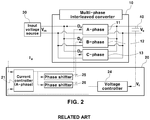
- FIGS. 1 and 2 are views showing current control methods of related art interleaved converters.
- V O represents an output voltage
- I A , I B and I C respectively represent phase currents
- D A , D B and D C respectively represent phase duty ratios (I X : X-phase current, and D X : X-phase duty ratio).
- I X X-phase current
- D X X-phase duty ratio
- the current control technique of a multi-phase interleaved converter uses two methods as shown in FIGS. 1 and 2 .
- the first method is most frequently used, and, as shown in FIG. 1 , is a method in which one voltage controller 24 is utilized, and as many current controllers 21, 22 and 23 are utilized as the number of the phases. That is, in this method, current controllers 21, 22 and 23 for the respective phases are utilized.
- the current controllers 21, 22 and 23 receive sensed currents I A , I B and I C of the phases to generate duty ratio signals D A , D B and D C for controlling converters for the phases, respectively. Further, the current controllers 21, 22 and 23 are individually applied, thereby achieving current balance.
- MICOM microcomputer
- the second method is a method in which one voltage controller 24 and one current controller 21 are utilized as shown in FIG. 2 .
- the current controller 21 receives sensed current I A of a first phase to generate a duty ratio D A by performing current control on the first phase, and the other phases are controlled by phase-shifting signals D B and D C having the same duty ratio to a predetermined size (different depending on the number of phases).
- the current controller 21 of the first phase is used, and hence changes in currents of the other phases are not instantaneously and exactly reflected. As a result, current imbalance may be created.
- the interleaved converter of FIG. 1 converts an output V IN output from an input voltage source 30, using a multi-phase interleaved converter 10, and transmits the converted output to an output terminal.
- an interleaved controller 20 controlling converters 11, 12 and 13 taking charge of the respective phases is provided with the current controllers 21, 22 and 23 for the converters 11, 12 and 13 taking charge of the respective phases. That is, a current controller 21 taking charge of phase A is provided to a sub-circuit 11 taking charge of the phase A, a current controller 22 taking charge of phase B is provided to a sub-circuit 12 taking charge of the phase B and, a current controller 23 taking charge of phase C is provided to a sub-circuit 13 taking charge of the phase C.
- the voltage controller 24 measures a voltage V O of an output terminal capacitor 40, and transmits the measured voltage to each of the current controllers 21, 22 and 23.
- the current controllers 21, 22 and 23 for the respective phases generate duty ratio signals D A , D B and D C controlling the respective phases, and transmit the generated duty ratios to the interleaved converter 10, thereby controlling current output from the converter.
- the current controllers 21, 22 and 23 taking charge of the respective phases facilitate a the balancing of the inductor.
- the load factor of the MICOM increases.
- FIG. 2 is a view showing a case where only one current controller is provided in the current control method.
- the interleaved converter of FIG. 2 also transmits an output V IN from the input voltage source 30 to an output terminal, using the multi-phase interleaved converter 10.
- the interleaved controller 20 controlling the converters 11, 12 and 13 taking charge of the respective phases is provided with only one current controller 21.
- the interleaved converters 12 and 13 of the other phases are controlled by phase-shifting an output signal from the one current controller 21. That is, when the current controller 21 takes charge of the phase A, the converters 12 and 13 respectively taking charge of the phases B and C can phase-shift the signal output from the current controller 21 taking charge of the phase A by 120 degrees and 240 degrees, using phase shifters 25 and 26, and the phase-shifted signals are used for controls of the phases B and C, respectively.
- a duty ratio D A for controlling current of one phase using the one current controller 21, and the other two phases are controlled by respectively phase-shifting signals D B and D C having the same duty ratio by 120 degrees and 240 degrees through phase shifters 25 and 26, respectively.
- the load factor of the MICOM can be reduced, but changes in currents of the other phases are not instantaneously and exactly reflected. Therefore, current imbalance may be created
- Document US201 3/320951 (WU Albert ) is, for example, a good prior art.
- the present disclosure provides a multi-phase interleaved converter which can effectively protect a power element by solving a problem of current imbalance between phases.
- the present disclosure also provides a multi-phase interleaved converter which can achieve an effect capable of solving current imbalance between phases, and reduce the load factor of a microprocessor (MICOM) by simplifying an operating process through the use of one current controller and one balancing controller.
- MICOM microprocessor
- the present disclosure provides a multi-phase interleaved converter, including: n sub-circuits of phases, configured to have inputs connected in parallel and outputs connected in parallel in order to convert a direct current (DC) or alternating current (AC) input voltage of one level into a DC or AC output voltage of another level; a current controller configured to: i) receive a current control command and a phase current value of a particular sub-circuit of a particular phase among the n sub-circuits of the respective phases and ii) output a control signal for controlling the particular sub-circuit of the particular phase; and a balancing controller configured to: i) receive phase current values of the n sub-circuits of the respective phases and a control signal output from the current controller and ii) adjust duty ratios of control signals applied to the other sub-circuits, based on the received phase current values of the sub-circuits of the respective phases and the received control signal of the current controller.
- DC direct current
- AC alternating current
- the present disclosure provides a method for controlling a multi-phase interleaved converter, the method including: sensing phase current values of n sub-circuits of the multi-phase interleaved converter; receiving, by a current controller, a current control command and a phase current value of a particular sub-circuit of a particular phase among the n sub-circuits of the respective phases; outputting, by the current controller, a control signal for controlling the particular sub-circuit of the particular phase; receiving, by a balancing controller, phase current values of the n sub-circuits of the respective phases and the control signal output from the current controller; and adjusting, by the balancing controller, duty ratios of control signals applied to the other sub-circuits based on the received phase current values of the sub-circuits of the respective phases and the received control signal of the current controller.
- the multi-phase interleaved converter according to the present disclosure has advantages as follows.
- the load factor of a MICOM it is possible to reduce the load factor of a MICOM.
- the number of MICOMs can be decreased as compared with the existing high-priced MICOMs, or the existing high-priced MICOMs can be replaced by low-priced MICOMs having low specifications, thereby saving costs.
- the load facture of the MICOM can be reduced as compared with the related art current control of each phase, thereby smoothly performing various controls.
- the inductor current that is output from the sub-circuits of the respective phases can be maintained in a balance state, thereby reducing ripples in the inductor current.
- the current referred to as inductor current is current transmitted as an output to the output terminal by the current controllers 21, 22 and 23 taking charge of the respective phases. Further, an instantaneous change in voltage/current of each phase can be reflected, thereby achieving a fast response.
- controller refers to a hardware device that can include, for example, a memory and a processor.
- the memory is configured to store program instructions
- the processor is configured to execute the program instructions to perform one or more processes which are described further below.
- FIG. 3 is a view showing a result obtained by comparing amplitudes of currents respectively output from sub-modules of a multi-phase interleaved converter according to an embodiment of the present disclosure.
- a sub-circuit may be referred to each branch of a converter (in the case of three phases of phases A, B and C, the multi-phases may be n phases) taking charge of phase A (first phase), phase B (second phase) or phase C (third phase).
- n sub-circuits are connected in parallel and outputs of the n sub-circuits are connected in parallel in order to convert a direct current (DC) or alternating current (AC) input voltage of one level into a DC or AC output voltage of another level.
- DC direct current
- AC alternating current
- Each branch may be implemented in the form of a half bridge or full bridge, using semiconductor switching elements.
- inductor current output from the sub-circuit taking charge of the phase B is greater than that output from the sub-circuit taking charge of the phase A
- inductor current output from the sub-circuit taking charge of the phase C is greater than that output from the sub-circuit taking charge of the phase B (I A ⁇ I B ⁇ I C ).
- the inductor current output from the sub-circuit taking charge of the phase B should be output later by 120 degrees in phase than that output from the sub-circuit taking charge of the phase A (in the case of the phase C, the inductor current output from the sub-circuit taking charge of the phase C should be output later by 120 degrees in phase than that output from the sub-circuit taking charge of the phase B).
- the sub-circuits have the same phase in order to efficiently compare the amplitudes of inductor currents output from the respective sub-circuits.
- a power element such as an insulated gate bipolar transistor (IGBT) employed as a semiconductor switching element in the sub-circuit of the phase B or C should take charge of a larger amount of conduction current, and therefore, an overload is applied to the power element.
- IGBT insulated gate bipolar transistor
- a deviation between the inductor currents output from the sub-circuits taking charge of the phases A, B and C is large, and therefore, the ripple of the entire output current becomes large.
- the duty of a control signal for controlling the sub-circuit of the phase A is increased, while the duty of a control signal for controlling the sub-circuit of the phase B or C is decreased.
- I C ⁇ I A ⁇ I B as shown in FIG. 3 (b) the duty of the phase C is increased, and the duty of the phase A or B is decreased.
- the duties of the respective phases are differently applied using a current error between the phases through a balancing controller.
- FIG. 4 is a view showing a state in which the duty ratios of control signals respectively applied to the sub-circuits of the multi-phase interleaved converter are controlled according to the embodiment of the present disclosure.
- the semiconductor switching element of the sub-circuit taking charge of the phase A performs an "On" process for a time longer than the current driving time
- the semiconductor switching element of the sub-circuit taking charge of the phase B or C performs the "On” process for a time shorter than the current driving time.
- the semiconductor switching element of the sub-circuit taking charge of the phase C performs the "On” process for a time longer than the current driving time, while the semiconductor switching element of the sub-circuit taking charge of the phase A or B performs the "On” process for a time shorter than the current driving time.
- the duties of the respective phases are differently applied using a current error between the phases through a balancing controller.
- the current imbalance state between the respective phases can be improved as shown in FIG. 5 .
- the phases have the same phase in order to compare the amplitudes of currents output from the respective sub-circuits of the phases.
- FIG. 6 is a view illustrating in detail the multi-phase interleaved converter for implementing the concept of the present disclosure, which illustrates an example in which the multi-phase interleaved converter is applied to the three phases A, B and C.
- the three-phase interleaved converter 100 may include a circuit topology implemented in a three-phase interleaved type, an interleaved controller 200, an input voltage source 300 (V IN ) and an output terminal capacitor 400.
- the circuit topology of the three-phase interleaved converter 100 according to the embodiment of the present disclosure may include a sub-circuit 110 taking charge of the phase A, a sub-circuit 120 taking charge of the phase B, and a sub-circuit 130 taking charge of the phase C.
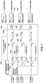
- the interleaved controller 200 applying a control signal to each of the sub-circuits 110, 120 and 130 may include a current controller 210, a balancing controller 220 positioned at the rear end of the current controller 210, phase shifters 231 and 232, and a voltage controller 240.
- the voltage controller 240 may receive output voltages of n sub-circuits, i.e., an output voltage V O of the output terminal capacitor 400 to transmit an output signal (e.g., current control command) that is in proportion to the amplitude of the received output voltage V O .
- the current controller 210 may receive the output signal (e.g., current control command) output from the voltage controller 240 and inductor current I A output from the sub-circuit 110 of one phase among the sub-circuits of the respective phases to generate and output a control signal D A for the one phase.
- the current controller 210 may receive I A that is current output from the sub-circuit 110 taking charge of the phase A and signal output from the voltage controller 240, and output, from the received current and signal, a duty ratio signal DA for controlling the sub-circuit 110 taking charge of the phase A.
- the balancing controller 220 has, as input information, current sensing information I A , I B and I C of the respective phases and the duty ratio (e.g., D A in FIG. 6 ) of an arbitrary one phase (e.g., the phase A in FIG. 6 , and the phase 1 in FIG. 6 ), which is an output of the current controller 210.
- a balance current command is set in the balancing controller 220, and sensed current of an arbitrary one phase is set as the balance current command.
- current e.g., I A that is current of the phase A in FIG. 6 , and sensing current of the phase 1 in FIG. 7
- used in the current controller 210 may be set as the balance current command.
- the balancing controller 220 may obtain and output duty ratios D B and D C for the other phases from the sensed currents I A , I B and I C of the respective phases, the duty ratio D A for the arbitrary one phase, and the balance current command I A .
- FIG. 7 is a view showing an internal control block of the balancing controller 220 in the multi-phases (n-phase) interleaved converter according to the embodiment of the present disclosure.
- phase 1, 2, 3, ..., n the phases in the multi-phase (n-phase) interleaved converter have been represented as phases 1, 2, 3, ..., n.
- the case where the phases 1, 2 and 3 are respectively represented as the phases A, B and C has been illustrated in FIG. 6 .
- the balancing controller 220 illustrated in FIG. 7 is set to use, as a balance current command, current of an arbitrary one phase among currents of the respective phases, i.e., current of the phase 1 (e.g., current of the phase A in FIG. 6 ), while receiving currents (currents of the n phases, and I A , I B and I C in FIG. 6 ) of the respective phases (the phases A, B and C in FIG. 6 ), which are sensed and output from sub-circuits (110, 120 130 in FIG. 6 ) taking charge of the respective phases (the phases 1, 2, 3, ..., n).
- the balancing controller 220 calculates, from input sensing information, errors between the balance current command and 2-phase current (B-phase current in FIG. 6 ), 3-phase current (C-phase current in FIG. 6 ), ..., n-phase current.
- the balancing controller 220 determines the duty ratios (2-phase duty ratio, 3-phase duty ratio, ..., n-phase duty ratio, and for example, D B and D C in FIG. 6 ) of control signals required to drive the sub-circuits (sub-circuits of the phases B and C, respectively designated by reference numerals 120 and 130 in FIG. 6 ) taking charge of the respective other phases (phases 2, 3, ..., n, and for example, the phases B and C in FIG. 6 ) except the phase 1 (e.g., the phase A in FIG. 6 ) by reflecting these errors.
- the phase-shifted control signals are applied to the respective sub-circuits (120 and 130 in FIG. 6 ).
- the multi-phase (n-phase) interleaved converter may go through a process of sensing currents (1-phase current, 2-phase current, 3-phase current, ..., n-phase current) output from the sub-circuits taking charge of the respective phases (phases 1, 2, 3, ..., n).
- the multi-phase (n-phase) interleaved converter calculates errors between the balance current command (1-phase current) and currents of the respective phases, and differently applies the duty ratios of control signals applied to the respective phases by reflecting the calculated errors.
- the multi-phase (n-phase) interleaved converter outputs the control signals of which duty ratios are adjusted as described above and applies the output control signals to the respective sub-circuits.
- the balancing controller 220 may receive currents of the respective phases, and obtain errors by subtracting a balance current command from the currents of the respective phases, using the current of any one phase (1-phase current) among the currents of the respective phases, which is used in generating the duty ratio in the current controller 210, as the balance current command. This process may be performed through adders 221.
- each error value may be amplified at a predetermined amplification rate.
- the error value may be amplified into gain values K p and K i . That is, this process may be performed through an amplifier 222 having the gain value K p and an amplifier 223 having the gain value K i .
- One of signals amplified with a predetermined value may be integrated through an integrator 224.
- the signal amplified with the value of K i may be amplified while passing through the amplifier 223.
- the values amplified through the predetermined gain value and a value among the amplified values, which is obtained through the integration process may pass through an adder 225, thereby obtaining ⁇ D that is a difference value between duty ratios to be adjusted.
- a process of obtaining a duty ratio to be appropriately adjusted from ⁇ D may be performed. That is, signals of the respective phases may be adjusted to 1- ⁇ D 2 , 1- ⁇ D 3 , ..., 1- ⁇ D n .
- the block for performing this process may be referred to as a duty adjuster 226.
- the signals may be multiplied by a signal output from the current controller 210 through a multiplier 227, thereby obtaining the duty ratios of control signals required to drive the sub-circuits taking charge of the respective phases except the phase 1.
- the driving signals for driving the sub-circuits taking charge of the phases 2, 3, ..., n may be respectively applied to semiconductor switching elements of the sub-circuits taking charge of the phases 2, 3, ..., n by phasing through the phase shifters 231 and 232. That is, the phases 2, 3, ..., n may be respectively delayed by 360/n ⁇ 1, 360/n ⁇ 2, ..., 360/n ⁇ (n-1) degrees with respect to the phase 1, to be input to the semiconductor switching elements of the sub-circuits taking charge of the respective phases.
- FIG. 7 illustrates a specific example in which the duty ratios of the respective phases are differently applied.
- error values between a balance current command and currents of the respective other phases except the arbitrary one phase e.g., the phase 1
- duty ratio difference values duty ratio correction values
- ⁇ D 2 , ⁇ D 3 , ..., ⁇ D n are then obtained
- the duty ratios of the respective other phases are obtained through a predetermined operation (addition, multiplication, subtraction, division, or the like), using the obtained values and the duty ratio of the arbitrary one phase (phase 1), thereby differently applying the duty ratios of the respective phases in the occurrence of current imbalance.
- the balancing controller may be configured to obtain difference values between the balance current command and current values from the sub-circuits of the respective other phases, obtain a duty ratio correction values by amplifying each difference value at a predetermined amplification rate K p , and then multiply the duty ratio of the control signal output from the current controller by the value obtained by subtracting the duty ratio correction value from 1, thereby applying the obtained control signal as a control signal to the sub-circuits of the other phases.
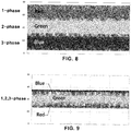
- FIGS. 8 and 9 are views comparing inductor currents before and after the multi-phase (three-phase) interleaved converter according to the embodiment of the present disclosure is applied.
- FIG. 8 is a graph showing inductor currents of the respective phases before the multi-phase (three-phase) interleaved converter according to the embodiment of the present disclosure is applied, i.e., in a state in which the balancing controller 220 is not provided.
- the red graph represents inductor current of the phase 1 (phase A)
- the green graph represents inductor current of the phase 2 (phase B)
- the blue graph represents inductor current of the phase 3 (phase C).
- FIG. 9 is a graph showing a result obtained by measuring current at the output terminal of the multi-phase (three-phase) interleaved converter to which the balancing converter 220 is applied according to the embodiment of the present disclosure.
- the red graph represents inductor current of the phase 1 (phase A)
- the green graph represents inductor current of the phase 2 (phase B)
- the blue graph represents inductor current of the phase 3 (phase C).
- FIG. 9 unlike the graph of FIG. 8 , the waveforms of the inductor currents of the respective phases almost correspond to one another.
- FIG. 7 illustrates an embodiment in which current of an arbitrary one phase is used as the balance current command.
- FIG. 10 illustrates an embodiment in which a separate balance current command generation block 228 for outputting a balance current command operated using one or multi-phase current information as an input is additionally provided in the balancing controller 220.
- the balance current command generation block 228 generates, as a balance current command, a value obtained through a predetermined operation from one or multi-phase current information, and the generated balance current command is used identically to that in the embodiment of FIG. 7 .
- the duty ratios of the respective phases are differently applied through the same process except that the separate balance current command generation block 228 is provided in the embodiment of FIG. 10 , and therefore, its detailed description will be omitted to avoid redundancy.
- FIG. 11 is a configuration view of a multi-phase interleaved converter according to another embodiment of the present disclosure.
- MICOM microprocessor
- a filter 500 for averaging sensing currents of each phase is additionally provided in the embodiment of FIG. 11 .
- the embodiment of FIG. 11 is not different from those of FIGS. 6 and 10 in function of components, operation processes, and the like, except that the filter 500 for each phase is additionally provided (in the case of n phases, n filters are provided).
- the balancing controller 220 uses, as input information, currents I A_filter , I B_filter and I C_filter averaged through the respective filters 500, rather than the sensed currents IA, I B and I C of the respective phases.
- FIG. 11 is not different from that of FIG. 5 in the operation process of the balancing controller 220, the phase shifting process of the phase shifters 231 and 232, and the like, except that the process of averaging current of each phase using the filter 500 is added, and therefore, their descriptions will be omitted to avoid redundancy.
- the current imbalance of the multi-phase interleaved converter may be caused by various hardware factors such as a processing tolerance of an inductor and a difference in resistance, and the current balance control does not require a fast response.
- the current for each phase, averaged using the simple filter 500 is transmitted as input information to the balancing controller 220, thereby performing the current balance control.
- the balance current control method of the interleave converter using the filter 500 it is possible to reduce the load factor of the MICOM by decreasing the operation time of the balancing controller 220 (applying the performance period capable of reducing the load factor). In addition, it is possible to prevent a problem of current imbalance between phases, which may occur in the interleaved converter, and overload and damage of a power element, caused by the current imbalance.
- FIG. 12 is a graph showing a result obtained by measuring current at the output terminal of the multi-phase interleaved converter in the embodiment of FIG. 11 .
- the red graph represents inductor current of the phase 1 (phase A)
- the green graph represents inductor current of the phase 2 (phase B)
- the blue graph represents inductor current of the phase 3 (phase C).
Landscapes
- Engineering & Computer Science (AREA)
- Power Engineering (AREA)
- Dc-Dc Converters (AREA)
- Ac-Ac Conversion (AREA)
- Rectifiers (AREA)
- Control Of Electrical Variables (AREA)
Applications Claiming Priority (1)
| Application Number | Priority Date | Filing Date | Title |
|---|---|---|---|
| KR1020140058241A KR101610469B1 (ko) | 2014-05-15 | 2014-05-15 | 다상 인터리브 컨버터 및 이의 제어 방법 |
Publications (3)
| Publication Number | Publication Date |
|---|---|
| EP2945267A2 EP2945267A2 (en) | 2015-11-18 |
| EP2945267A3 EP2945267A3 (en) | 2015-12-02 |
| EP2945267B1 true EP2945267B1 (en) | 2018-05-23 |
Family
ID=52002845
Family Applications (1)
| Application Number | Title | Priority Date | Filing Date |
|---|---|---|---|
| EP14196268.8A Active EP2945267B1 (en) | 2014-05-15 | 2014-12-04 | Multi-phase interleaved converter and control method thereof |
Country Status (5)
| Country | Link |
|---|---|
| US (1) | US9698692B2 (ko) |
| EP (1) | EP2945267B1 (ko) |
| JP (1) | JP6474595B2 (ko) |
| KR (1) | KR101610469B1 (ko) |
| CN (1) | CN105099152B (ko) |
Cited By (1)
| Publication number | Priority date | Publication date | Assignee | Title |
|---|---|---|---|---|
| US11329564B2 (en) | 2019-06-14 | 2022-05-10 | Samsung Sdi Co., Ltd. | Control system for a battery system |
Families Citing this family (18)
| Publication number | Priority date | Publication date | Assignee | Title |
|---|---|---|---|---|
| WO2018047691A1 (ja) * | 2016-09-12 | 2018-03-15 | 株式会社村田製作所 | 電源装置 |
| FR3056852B1 (fr) * | 2016-09-27 | 2018-09-28 | Renault S.A.S | Procede de commande d'un redresseur triphase pour un dispositif de charge embarque sur un vehicule electrique ou hybride |
| JPWO2018066042A1 (ja) * | 2016-10-03 | 2019-07-25 | 本田技研工業株式会社 | 変換装置、機器及び制御方法 |
| JP6873687B2 (ja) | 2016-12-27 | 2021-05-19 | 株式会社京三製作所 | 電源装置、及び電源装置の制御方法 |
| JP6749231B2 (ja) | 2016-12-27 | 2020-09-02 | 株式会社京三製作所 | 電源装置、及び電源装置の制御方法 |
| JP6947504B2 (ja) | 2016-12-27 | 2021-10-13 | 株式会社京三製作所 | 電源装置、及び電源装置の制御方法 |
| JP6712547B2 (ja) | 2016-12-27 | 2020-06-24 | 株式会社京三製作所 | 電源装置、及び電源装置の制御方法 |
| KR102395035B1 (ko) * | 2017-08-29 | 2022-05-13 | 삼성전자 주식회사 | 전류 편차를 보상하기 위한 전원 공급 장치 및 이의 동작 방법 |
| KR102099975B1 (ko) * | 2018-04-18 | 2020-04-13 | 현대종합금속 주식회사 | 전류제어를 통해 리플을 저감시키는 병렬 정류기 |
| DE112018007516T5 (de) * | 2018-04-25 | 2021-01-14 | Mitsubishi Electric Corporation | Leistungsumwandlungsvorrichtung |
| KR102611984B1 (ko) | 2018-10-10 | 2023-12-08 | 삼성전자주식회사 | 인터리빙 회로를 포함하는 다상 스위칭 레귤레이터 및 이의 스위칭 레귤레이팅 방법 |
| US11190101B2 (en) * | 2018-10-30 | 2021-11-30 | Lear Corporation | System and method for balancing current of converter phases |
| DE102018219277A1 (de) | 2018-11-12 | 2020-05-14 | Kaco New Energy Gmbh | Verfahren zum Betreiben eines PV-Wechselrichters und PV-Wechselrichter |
| KR102091589B1 (ko) | 2019-02-18 | 2020-03-20 | 주식회사 효원파워텍 | 상간 위상 제어 방식을 이용한 다상 모터 제어 시스템의 공통 모드 전압 저감 장치 |
| CN114651388A (zh) | 2019-11-14 | 2022-06-21 | 三菱电机株式会社 | 电力变换装置、马达驱动装置、送风机、压缩机以及空气调节机 |
| US11043891B1 (en) * | 2020-01-23 | 2021-06-22 | Hong Kong Applied Science and Technology Research Institute Company Limited | Controller for an AC/DC or a DC/AC multi-phase power converter |
| KR102644445B1 (ko) * | 2021-11-16 | 2024-03-06 | 계명대학교 산학협력단 | 충전 시 전기차용 배터리의 전류 리플 제거를 위한 위상 천이 풀 브릿지 컨버터 및 그 이용 방법 |
| US11990827B2 (en) * | 2022-01-24 | 2024-05-21 | Aes Global Holdings Pte Ltd. | Current balancing for interleaved power stages |
Family Cites Families (21)
| Publication number | Priority date | Publication date | Assignee | Title |
|---|---|---|---|---|
| JPH09331682A (ja) | 1996-06-12 | 1997-12-22 | Meidensha Corp | 電力変換器 |
| JPH10257773A (ja) | 1997-03-13 | 1998-09-25 | Brother Ind Ltd | 電力変換装置 |
| US6278263B1 (en) | 1999-09-01 | 2001-08-21 | Intersil Corporation | Multi-phase converter with balanced currents |
| US6215290B1 (en) * | 1999-11-15 | 2001-04-10 | Semtech Corporation | Multi-phase and multi-module power supplies with balanced current between phases and modules |
| KR100836180B1 (ko) | 2006-11-30 | 2008-06-09 | 한국항공우주연구원 | 출력전압 리플을 저감하는 병렬형 컨버터 시스템 및 그제어방법 |
| JP5097453B2 (ja) | 2007-06-06 | 2012-12-12 | 三菱電機株式会社 | 電力変換装置 |
| JP5230207B2 (ja) | 2008-01-07 | 2013-07-10 | 三菱重工業株式会社 | 双方向電力変換器およびその制御方法 |
| JP5075749B2 (ja) * | 2008-06-19 | 2012-11-21 | 本田技研工業株式会社 | Dc/dcコンバータ装置、ハイブリッド直流電源システム、電気車両及びdc/dcコンバータの制御方法 |
| US8120205B2 (en) * | 2008-07-18 | 2012-02-21 | Zilker Labs, Inc. | Adding and dropping phases in current sharing |
| US8239597B2 (en) * | 2008-07-18 | 2012-08-07 | Intersil Americas Inc. | Device-to-device communication bus for distributed power management |
| KR101034263B1 (ko) | 2008-12-29 | 2011-05-16 | 한국전기연구원 | 태양광 발전용 dc-dc 컨버터 |
| US8970195B2 (en) * | 2009-06-10 | 2015-03-03 | Stmicroelectronics S.R.L. | Method for controlling an interleaving multiphase regulator and corresponding system |
| CN101699740B (zh) * | 2009-10-15 | 2011-08-24 | 旭丽电子(广州)有限公司 | 电源供应装置 |
| US8441241B2 (en) * | 2010-05-03 | 2013-05-14 | Intel Corporation | Methods and systems to digitally balance currents of a multi-phase voltage regulator |
| US8624567B2 (en) * | 2011-12-30 | 2014-01-07 | O2Micro, Inc. | Controllers for DC/DC converters |
| US9077243B2 (en) | 2012-01-31 | 2015-07-07 | Analog Devices, Inc. | Current-balancing in interleaved circuit phases using a parameter common to the phases |
| JP5643777B2 (ja) * | 2012-02-21 | 2014-12-17 | 株式会社東芝 | マルチフェーズ・スイッチング電源回路 |
| US9077244B2 (en) * | 2012-05-30 | 2015-07-07 | Linear Technology Corporation | Expanding DC/DC converter into multiphase DC/DC converter |
| JP5847022B2 (ja) * | 2012-06-11 | 2016-01-20 | 三菱電機株式会社 | 空気調和機、およびそのインターリーブ制御方法 |
| CN103248231B (zh) * | 2013-04-02 | 2015-12-23 | 浙江大学 | 多相均流控制的并联调整电路控制方法 |
| JP5717838B2 (ja) * | 2013-12-26 | 2015-05-13 | 三菱電機株式会社 | 電力変換装置 |
-
2014
- 2014-05-15 KR KR1020140058241A patent/KR101610469B1/ko active IP Right Grant
- 2014-12-04 EP EP14196268.8A patent/EP2945267B1/en active Active
- 2014-12-04 JP JP2014245869A patent/JP6474595B2/ja active Active
- 2014-12-06 US US14/562,696 patent/US9698692B2/en active Active
- 2014-12-15 CN CN201410776681.0A patent/CN105099152B/zh active Active
Non-Patent Citations (1)
| Title |
|---|
| None * |
Cited By (1)
| Publication number | Priority date | Publication date | Assignee | Title |
|---|---|---|---|---|
| US11329564B2 (en) | 2019-06-14 | 2022-05-10 | Samsung Sdi Co., Ltd. | Control system for a battery system |
Also Published As
| Publication number | Publication date |
|---|---|
| JP2015220976A (ja) | 2015-12-07 |
| EP2945267A2 (en) | 2015-11-18 |
| CN105099152A (zh) | 2015-11-25 |
| EP2945267A3 (en) | 2015-12-02 |
| KR101610469B1 (ko) | 2016-04-07 |
| US20150333629A1 (en) | 2015-11-19 |
| US9698692B2 (en) | 2017-07-04 |
| JP6474595B2 (ja) | 2019-02-27 |
| CN105099152B (zh) | 2019-06-07 |
| KR20150131512A (ko) | 2015-11-25 |
Similar Documents
| Publication | Publication Date | Title |
|---|---|---|
| EP2945267B1 (en) | Multi-phase interleaved converter and control method thereof | |
| US9531272B2 (en) | Two-phase interleaved converter and method of controlling the same | |
| US7977898B2 (en) | Current sensing for a multi-phase DC/DC boost converter | |
| CN108028599B (zh) | 控制三相电力转换器 | |
| JP5161985B2 (ja) | 電力変換装置および電動パワーステアリングの制御装置 | |
| WO2013080744A1 (ja) | マトリクスコンバータ | |
| US10305373B2 (en) | Input reference signal generation systems and methods | |
| WO2019207747A1 (ja) | スイッチング電源装置 | |
| EP3522363A1 (en) | Control device for power converter | |
| US20140233276A1 (en) | Power converter control method | |
| JP2014143786A (ja) | 電力変換装置 | |
| US11529993B2 (en) | Motor controller and electric power steering apparatus | |
| JP2022031962A (ja) | スイッチング電源装置 | |
| WO2018131086A1 (ja) | 電力変換装置 | |
| WO2016114330A1 (ja) | 5レベル電力変換器および制御方法 | |
| CN116865543A (zh) | 交错pfc电路的均流控制方法、控制装置及存储介 | |
| KR101592744B1 (ko) | 다상 인터리브 컨버터의 전류 제어 방법 및 장치 | |
| JP4844180B2 (ja) | 電力変換器およびその制御方法 | |
| JP4649940B2 (ja) | コンバータの制御方法及びコンバータの制御装置 | |
| JP7211097B2 (ja) | 電力制御方法、及び、電力制御装置 | |
| KR20180078772A (ko) | Pfc 부스트 컨버터 및 그 제어방법 | |
| JP6410681B2 (ja) | 電力変換装置 | |
| KR101783915B1 (ko) | 교류 전동기 제어 장치 및 방법 | |
| JP2021078176A (ja) | 回転電動機の制御装置 | |
| JP2022020373A (ja) | 電力変換装置及びその制御方法 |
Legal Events
| Date | Code | Title | Description |
|---|---|---|---|
| PUAL | Search report despatched |
Free format text: ORIGINAL CODE: 0009013 |
|
| PUAI | Public reference made under article 153(3) epc to a published international application that has entered the european phase |
Free format text: ORIGINAL CODE: 0009012 |
|
| AK | Designated contracting states |
Kind code of ref document: A2 Designated state(s): AL AT BE BG CH CY CZ DE DK EE ES FI FR GB GR HR HU IE IS IT LI LT LU LV MC MK MT NL NO PL PT RO RS SE SI SK SM TR |
|
| AX | Request for extension of the european patent |
Extension state: BA ME |
|
| AK | Designated contracting states |
Kind code of ref document: A3 Designated state(s): AL AT BE BG CH CY CZ DE DK EE ES FI FR GB GR HR HU IE IS IT LI LT LU LV MC MK MT NL NO PL PT RO RS SE SI SK SM TR |
|
| AX | Request for extension of the european patent |
Extension state: BA ME |
|
| RIC1 | Information provided on ipc code assigned before grant |
Ipc: H02M 1/00 20070101AFI20151029BHEP Ipc: H02M 1/14 20060101ALI20151029BHEP |
|
| 17P | Request for examination filed |
Effective date: 20160602 |
|
| RBV | Designated contracting states (corrected) |
Designated state(s): AL AT BE BG CH CY CZ DE DK EE ES FI FR GB GR HR HU IE IS IT LI LT LU LV MC MK MT NL NO PL PT RO RS SE SI SK SM TR |
|
| RIC1 | Information provided on ipc code assigned before grant |
Ipc: H02M 1/14 20060101ALI20170927BHEP Ipc: H02M 1/00 20070101AFI20170927BHEP |
|
| GRAP | Despatch of communication of intention to grant a patent |
Free format text: ORIGINAL CODE: EPIDOSNIGR1 |
|
| STAA | Information on the status of an ep patent application or granted ep patent |
Free format text: STATUS: GRANT OF PATENT IS INTENDED |
|
| INTG | Intention to grant announced |
Effective date: 20171205 |
|
| GRAS | Grant fee paid |
Free format text: ORIGINAL CODE: EPIDOSNIGR3 |
|
| GRAA | (expected) grant |
Free format text: ORIGINAL CODE: 0009210 |
|
| STAA | Information on the status of an ep patent application or granted ep patent |
Free format text: STATUS: THE PATENT HAS BEEN GRANTED |
|
| AK | Designated contracting states |
Kind code of ref document: B1 Designated state(s): AL AT BE BG CH CY CZ DE DK EE ES FI FR GB GR HR HU IE IS IT LI LT LU LV MC MK MT NL NO PL PT RO RS SE SI SK SM TR |
|
| REG | Reference to a national code |
Ref country code: GB Ref legal event code: FG4D |
|
| REG | Reference to a national code |
Ref country code: CH Ref legal event code: EP |
|
| REG | Reference to a national code |
Ref country code: IE Ref legal event code: FG4D |
|
| REG | Reference to a national code |
Ref country code: AT Ref legal event code: REF Ref document number: 1002315 Country of ref document: AT Kind code of ref document: T Effective date: 20180615 |
|
| REG | Reference to a national code |
Ref country code: DE Ref legal event code: R096 Ref document number: 602014025801 Country of ref document: DE |
|
| REG | Reference to a national code |
Ref country code: NL Ref legal event code: MP Effective date: 20180523 |
|
| REG | Reference to a national code |
Ref country code: LT Ref legal event code: MG4D |
|
| PG25 | Lapsed in a contracting state [announced via postgrant information from national office to epo] |
Ref country code: SE Free format text: LAPSE BECAUSE OF FAILURE TO SUBMIT A TRANSLATION OF THE DESCRIPTION OR TO PAY THE FEE WITHIN THE PRESCRIBED TIME-LIMIT Effective date: 20180523 Ref country code: FI Free format text: LAPSE BECAUSE OF FAILURE TO SUBMIT A TRANSLATION OF THE DESCRIPTION OR TO PAY THE FEE WITHIN THE PRESCRIBED TIME-LIMIT Effective date: 20180523 Ref country code: BG Free format text: LAPSE BECAUSE OF FAILURE TO SUBMIT A TRANSLATION OF THE DESCRIPTION OR TO PAY THE FEE WITHIN THE PRESCRIBED TIME-LIMIT Effective date: 20180823 Ref country code: NO Free format text: LAPSE BECAUSE OF FAILURE TO SUBMIT A TRANSLATION OF THE DESCRIPTION OR TO PAY THE FEE WITHIN THE PRESCRIBED TIME-LIMIT Effective date: 20180823 Ref country code: ES Free format text: LAPSE BECAUSE OF FAILURE TO SUBMIT A TRANSLATION OF THE DESCRIPTION OR TO PAY THE FEE WITHIN THE PRESCRIBED TIME-LIMIT Effective date: 20180523 Ref country code: LT Free format text: LAPSE BECAUSE OF FAILURE TO SUBMIT A TRANSLATION OF THE DESCRIPTION OR TO PAY THE FEE WITHIN THE PRESCRIBED TIME-LIMIT Effective date: 20180523 |
|
| PG25 | Lapsed in a contracting state [announced via postgrant information from national office to epo] |
Ref country code: GR Free format text: LAPSE BECAUSE OF FAILURE TO SUBMIT A TRANSLATION OF THE DESCRIPTION OR TO PAY THE FEE WITHIN THE PRESCRIBED TIME-LIMIT Effective date: 20180824 Ref country code: RS Free format text: LAPSE BECAUSE OF FAILURE TO SUBMIT A TRANSLATION OF THE DESCRIPTION OR TO PAY THE FEE WITHIN THE PRESCRIBED TIME-LIMIT Effective date: 20180523 Ref country code: HR Free format text: LAPSE BECAUSE OF FAILURE TO SUBMIT A TRANSLATION OF THE DESCRIPTION OR TO PAY THE FEE WITHIN THE PRESCRIBED TIME-LIMIT Effective date: 20180523 Ref country code: NL Free format text: LAPSE BECAUSE OF FAILURE TO SUBMIT A TRANSLATION OF THE DESCRIPTION OR TO PAY THE FEE WITHIN THE PRESCRIBED TIME-LIMIT Effective date: 20180523 Ref country code: LV Free format text: LAPSE BECAUSE OF FAILURE TO SUBMIT A TRANSLATION OF THE DESCRIPTION OR TO PAY THE FEE WITHIN THE PRESCRIBED TIME-LIMIT Effective date: 20180523 |
|
| REG | Reference to a national code |
Ref country code: AT Ref legal event code: MK05 Ref document number: 1002315 Country of ref document: AT Kind code of ref document: T Effective date: 20180523 |
|
| PG25 | Lapsed in a contracting state [announced via postgrant information from national office to epo] |
Ref country code: AT Free format text: LAPSE BECAUSE OF FAILURE TO SUBMIT A TRANSLATION OF THE DESCRIPTION OR TO PAY THE FEE WITHIN THE PRESCRIBED TIME-LIMIT Effective date: 20180523 Ref country code: CZ Free format text: LAPSE BECAUSE OF FAILURE TO SUBMIT A TRANSLATION OF THE DESCRIPTION OR TO PAY THE FEE WITHIN THE PRESCRIBED TIME-LIMIT Effective date: 20180523 Ref country code: RO Free format text: LAPSE BECAUSE OF FAILURE TO SUBMIT A TRANSLATION OF THE DESCRIPTION OR TO PAY THE FEE WITHIN THE PRESCRIBED TIME-LIMIT Effective date: 20180523 Ref country code: EE Free format text: LAPSE BECAUSE OF FAILURE TO SUBMIT A TRANSLATION OF THE DESCRIPTION OR TO PAY THE FEE WITHIN THE PRESCRIBED TIME-LIMIT Effective date: 20180523 Ref country code: PL Free format text: LAPSE BECAUSE OF FAILURE TO SUBMIT A TRANSLATION OF THE DESCRIPTION OR TO PAY THE FEE WITHIN THE PRESCRIBED TIME-LIMIT Effective date: 20180523 Ref country code: DK Free format text: LAPSE BECAUSE OF FAILURE TO SUBMIT A TRANSLATION OF THE DESCRIPTION OR TO PAY THE FEE WITHIN THE PRESCRIBED TIME-LIMIT Effective date: 20180523 Ref country code: SK Free format text: LAPSE BECAUSE OF FAILURE TO SUBMIT A TRANSLATION OF THE DESCRIPTION OR TO PAY THE FEE WITHIN THE PRESCRIBED TIME-LIMIT Effective date: 20180523 |
|
| REG | Reference to a national code |
Ref country code: DE Ref legal event code: R097 Ref document number: 602014025801 Country of ref document: DE |
|
| PG25 | Lapsed in a contracting state [announced via postgrant information from national office to epo] |
Ref country code: SM Free format text: LAPSE BECAUSE OF FAILURE TO SUBMIT A TRANSLATION OF THE DESCRIPTION OR TO PAY THE FEE WITHIN THE PRESCRIBED TIME-LIMIT Effective date: 20180523 Ref country code: IT Free format text: LAPSE BECAUSE OF FAILURE TO SUBMIT A TRANSLATION OF THE DESCRIPTION OR TO PAY THE FEE WITHIN THE PRESCRIBED TIME-LIMIT Effective date: 20180523 |
|
| PLBE | No opposition filed within time limit |
Free format text: ORIGINAL CODE: 0009261 |
|
| STAA | Information on the status of an ep patent application or granted ep patent |
Free format text: STATUS: NO OPPOSITION FILED WITHIN TIME LIMIT |
|
| 26N | No opposition filed |
Effective date: 20190226 |
|
| PG25 | Lapsed in a contracting state [announced via postgrant information from national office to epo] |
Ref country code: SI Free format text: LAPSE BECAUSE OF FAILURE TO SUBMIT A TRANSLATION OF THE DESCRIPTION OR TO PAY THE FEE WITHIN THE PRESCRIBED TIME-LIMIT Effective date: 20180523 |
|
| REG | Reference to a national code |
Ref country code: CH Ref legal event code: PL |
|
| PG25 | Lapsed in a contracting state [announced via postgrant information from national office to epo] |
Ref country code: MC Free format text: LAPSE BECAUSE OF FAILURE TO SUBMIT A TRANSLATION OF THE DESCRIPTION OR TO PAY THE FEE WITHIN THE PRESCRIBED TIME-LIMIT Effective date: 20180523 Ref country code: LU Free format text: LAPSE BECAUSE OF NON-PAYMENT OF DUE FEES Effective date: 20181204 |
|
| REG | Reference to a national code |
Ref country code: IE Ref legal event code: MM4A |
|
| REG | Reference to a national code |
Ref country code: BE Ref legal event code: MM Effective date: 20181231 |
|
| PG25 | Lapsed in a contracting state [announced via postgrant information from national office to epo] |
Ref country code: IE Free format text: LAPSE BECAUSE OF NON-PAYMENT OF DUE FEES Effective date: 20181204 |
|
| PG25 | Lapsed in a contracting state [announced via postgrant information from national office to epo] |
Ref country code: AL Free format text: LAPSE BECAUSE OF FAILURE TO SUBMIT A TRANSLATION OF THE DESCRIPTION OR TO PAY THE FEE WITHIN THE PRESCRIBED TIME-LIMIT Effective date: 20180523 Ref country code: BE Free format text: LAPSE BECAUSE OF NON-PAYMENT OF DUE FEES Effective date: 20181231 |
|
| PG25 | Lapsed in a contracting state [announced via postgrant information from national office to epo] |
Ref country code: CH Free format text: LAPSE BECAUSE OF NON-PAYMENT OF DUE FEES Effective date: 20181231 Ref country code: LI Free format text: LAPSE BECAUSE OF NON-PAYMENT OF DUE FEES Effective date: 20181231 |
|
| PG25 | Lapsed in a contracting state [announced via postgrant information from national office to epo] |
Ref country code: MT Free format text: LAPSE BECAUSE OF NON-PAYMENT OF DUE FEES Effective date: 20181204 |
|
| PG25 | Lapsed in a contracting state [announced via postgrant information from national office to epo] |
Ref country code: TR Free format text: LAPSE BECAUSE OF FAILURE TO SUBMIT A TRANSLATION OF THE DESCRIPTION OR TO PAY THE FEE WITHIN THE PRESCRIBED TIME-LIMIT Effective date: 20180523 |
|
| PG25 | Lapsed in a contracting state [announced via postgrant information from national office to epo] |
Ref country code: PT Free format text: LAPSE BECAUSE OF FAILURE TO SUBMIT A TRANSLATION OF THE DESCRIPTION OR TO PAY THE FEE WITHIN THE PRESCRIBED TIME-LIMIT Effective date: 20180523 |
|
| PG25 | Lapsed in a contracting state [announced via postgrant information from national office to epo] |
Ref country code: CY Free format text: LAPSE BECAUSE OF FAILURE TO SUBMIT A TRANSLATION OF THE DESCRIPTION OR TO PAY THE FEE WITHIN THE PRESCRIBED TIME-LIMIT Effective date: 20180523 Ref country code: HU Free format text: LAPSE BECAUSE OF FAILURE TO SUBMIT A TRANSLATION OF THE DESCRIPTION OR TO PAY THE FEE WITHIN THE PRESCRIBED TIME-LIMIT; INVALID AB INITIO Effective date: 20141204 Ref country code: MK Free format text: LAPSE BECAUSE OF NON-PAYMENT OF DUE FEES Effective date: 20180523 |
|
| PG25 | Lapsed in a contracting state [announced via postgrant information from national office to epo] |
Ref country code: IS Free format text: LAPSE BECAUSE OF FAILURE TO SUBMIT A TRANSLATION OF THE DESCRIPTION OR TO PAY THE FEE WITHIN THE PRESCRIBED TIME-LIMIT Effective date: 20180923 |
|
| P01 | Opt-out of the competence of the unified patent court (upc) registered |
Effective date: 20230511 |
|
| PGFP | Annual fee paid to national office [announced via postgrant information from national office to epo] |
Ref country code: GB Payment date: 20231120 Year of fee payment: 10 |
|
| PGFP | Annual fee paid to national office [announced via postgrant information from national office to epo] |
Ref country code: FR Payment date: 20231121 Year of fee payment: 10 Ref country code: DE Payment date: 20231120 Year of fee payment: 10 |