EP2931008A1 - Leiterplatte und herstellungsverfahren dafür - Google Patents
Leiterplatte und herstellungsverfahren dafür Download PDFInfo
- Publication number
- EP2931008A1 EP2931008A1 EP13861374.0A EP13861374A EP2931008A1 EP 2931008 A1 EP2931008 A1 EP 2931008A1 EP 13861374 A EP13861374 A EP 13861374A EP 2931008 A1 EP2931008 A1 EP 2931008A1
- Authority
- EP
- European Patent Office
- Prior art keywords
- layer
- forming
- substitution
- plating
- double
- Prior art date
- Legal status (The legal status is an assumption and is not a legal conclusion. Google has not performed a legal analysis and makes no representation as to the accuracy of the status listed.)
- Withdrawn
Links
Images


Classifications
-
- H—ELECTRICITY
- H05—ELECTRIC TECHNIQUES NOT OTHERWISE PROVIDED FOR
- H05K—PRINTED CIRCUITS; CASINGS OR CONSTRUCTIONAL DETAILS OF ELECTRIC APPARATUS; MANUFACTURE OF ASSEMBLAGES OF ELECTRICAL COMPONENTS
- H05K1/00—Printed circuits
- H05K1/02—Details
- H05K1/0296—Conductive pattern lay-out details not covered by sub groups H05K1/02 - H05K1/0295
- H05K1/0298—Multilayer circuits
-
- C—CHEMISTRY; METALLURGY
- C23—COATING METALLIC MATERIAL; COATING MATERIAL WITH METALLIC MATERIAL; CHEMICAL SURFACE TREATMENT; DIFFUSION TREATMENT OF METALLIC MATERIAL; COATING BY VACUUM EVAPORATION, BY SPUTTERING, BY ION IMPLANTATION OR BY CHEMICAL VAPOUR DEPOSITION, IN GENERAL; INHIBITING CORROSION OF METALLIC MATERIAL OR INCRUSTATION IN GENERAL
- C23C—COATING METALLIC MATERIAL; COATING MATERIAL WITH METALLIC MATERIAL; SURFACE TREATMENT OF METALLIC MATERIAL BY DIFFUSION INTO THE SURFACE, BY CHEMICAL CONVERSION OR SUBSTITUTION; COATING BY VACUUM EVAPORATION, BY SPUTTERING, BY ION IMPLANTATION OR BY CHEMICAL VAPOUR DEPOSITION, IN GENERAL
- C23C18/00—Chemical coating by decomposition of either liquid compounds or solutions of the coating forming compounds, without leaving reaction products of surface material in the coating; Contact plating
- C23C18/16—Chemical coating by decomposition of either liquid compounds or solutions of the coating forming compounds, without leaving reaction products of surface material in the coating; Contact plating by reduction or substitution, e.g. electroless plating
- C23C18/1601—Process or apparatus
- C23C18/1633—Process of electroless plating
- C23C18/1635—Composition of the substrate
- C23C18/1637—Composition of the substrate metallic substrate
-
- H—ELECTRICITY
- H05—ELECTRIC TECHNIQUES NOT OTHERWISE PROVIDED FOR
- H05K—PRINTED CIRCUITS; CASINGS OR CONSTRUCTIONAL DETAILS OF ELECTRIC APPARATUS; MANUFACTURE OF ASSEMBLAGES OF ELECTRICAL COMPONENTS
- H05K1/00—Printed circuits
- H05K1/02—Details
- H05K1/09—Use of materials for the conductive, e.g. metallic pattern
-
- C—CHEMISTRY; METALLURGY
- C23—COATING METALLIC MATERIAL; COATING MATERIAL WITH METALLIC MATERIAL; CHEMICAL SURFACE TREATMENT; DIFFUSION TREATMENT OF METALLIC MATERIAL; COATING BY VACUUM EVAPORATION, BY SPUTTERING, BY ION IMPLANTATION OR BY CHEMICAL VAPOUR DEPOSITION, IN GENERAL; INHIBITING CORROSION OF METALLIC MATERIAL OR INCRUSTATION IN GENERAL
- C23C—COATING METALLIC MATERIAL; COATING MATERIAL WITH METALLIC MATERIAL; SURFACE TREATMENT OF METALLIC MATERIAL BY DIFFUSION INTO THE SURFACE, BY CHEMICAL CONVERSION OR SUBSTITUTION; COATING BY VACUUM EVAPORATION, BY SPUTTERING, BY ION IMPLANTATION OR BY CHEMICAL VAPOUR DEPOSITION, IN GENERAL
- C23C18/00—Chemical coating by decomposition of either liquid compounds or solutions of the coating forming compounds, without leaving reaction products of surface material in the coating; Contact plating
- C23C18/16—Chemical coating by decomposition of either liquid compounds or solutions of the coating forming compounds, without leaving reaction products of surface material in the coating; Contact plating by reduction or substitution, e.g. electroless plating
- C23C18/1601—Process or apparatus
- C23C18/1633—Process of electroless plating
- C23C18/1646—Characteristics of the product obtained
- C23C18/165—Multilayered product
- C23C18/1653—Two or more layers with at least one layer obtained by electroless plating and one layer obtained by electroplating
-
- C—CHEMISTRY; METALLURGY
- C23—COATING METALLIC MATERIAL; COATING MATERIAL WITH METALLIC MATERIAL; CHEMICAL SURFACE TREATMENT; DIFFUSION TREATMENT OF METALLIC MATERIAL; COATING BY VACUUM EVAPORATION, BY SPUTTERING, BY ION IMPLANTATION OR BY CHEMICAL VAPOUR DEPOSITION, IN GENERAL; INHIBITING CORROSION OF METALLIC MATERIAL OR INCRUSTATION IN GENERAL
- C23C—COATING METALLIC MATERIAL; COATING MATERIAL WITH METALLIC MATERIAL; SURFACE TREATMENT OF METALLIC MATERIAL BY DIFFUSION INTO THE SURFACE, BY CHEMICAL CONVERSION OR SUBSTITUTION; COATING BY VACUUM EVAPORATION, BY SPUTTERING, BY ION IMPLANTATION OR BY CHEMICAL VAPOUR DEPOSITION, IN GENERAL
- C23C18/00—Chemical coating by decomposition of either liquid compounds or solutions of the coating forming compounds, without leaving reaction products of surface material in the coating; Contact plating
- C23C18/54—Contact plating, i.e. electroless electrochemical plating
-
- C—CHEMISTRY; METALLURGY
- C25—ELECTROLYTIC OR ELECTROPHORETIC PROCESSES; APPARATUS THEREFOR
- C25D—PROCESSES FOR THE ELECTROLYTIC OR ELECTROPHORETIC PRODUCTION OF COATINGS; ELECTROFORMING; APPARATUS THEREFOR
- C25D5/00—Electroplating characterised by the process; Pretreatment or after-treatment of workpieces
- C25D5/02—Electroplating of selected surface areas
-
- H—ELECTRICITY
- H05—ELECTRIC TECHNIQUES NOT OTHERWISE PROVIDED FOR
- H05K—PRINTED CIRCUITS; CASINGS OR CONSTRUCTIONAL DETAILS OF ELECTRIC APPARATUS; MANUFACTURE OF ASSEMBLAGES OF ELECTRICAL COMPONENTS
- H05K1/00—Printed circuits
- H05K1/02—Details
- H05K1/11—Printed elements for providing electric connections to or between printed circuits
- H05K1/115—Via connections; Lands around holes or via connections
-
- H—ELECTRICITY
- H05—ELECTRIC TECHNIQUES NOT OTHERWISE PROVIDED FOR
- H05K—PRINTED CIRCUITS; CASINGS OR CONSTRUCTIONAL DETAILS OF ELECTRIC APPARATUS; MANUFACTURE OF ASSEMBLAGES OF ELECTRICAL COMPONENTS
- H05K3/00—Apparatus or processes for manufacturing printed circuits
- H05K3/02—Apparatus or processes for manufacturing printed circuits in which the conductive material is applied to the surface of the insulating support and is thereafter removed from such areas of the surface which are not intended for current conducting or shielding
- H05K3/06—Apparatus or processes for manufacturing printed circuits in which the conductive material is applied to the surface of the insulating support and is thereafter removed from such areas of the surface which are not intended for current conducting or shielding the conductive material being removed chemically or electrolytically, e.g. by photo-etch process
-
- H—ELECTRICITY
- H05—ELECTRIC TECHNIQUES NOT OTHERWISE PROVIDED FOR
- H05K—PRINTED CIRCUITS; CASINGS OR CONSTRUCTIONAL DETAILS OF ELECTRIC APPARATUS; MANUFACTURE OF ASSEMBLAGES OF ELECTRICAL COMPONENTS
- H05K3/00—Apparatus or processes for manufacturing printed circuits
- H05K3/40—Forming printed elements for providing electric connections to or between printed circuits
- H05K3/42—Plated through-holes or plated via connections
- H05K3/429—Plated through-holes specially for multilayer circuits, e.g. having connections to inner circuit layers
-
- H—ELECTRICITY
- H05—ELECTRIC TECHNIQUES NOT OTHERWISE PROVIDED FOR
- H05K—PRINTED CIRCUITS; CASINGS OR CONSTRUCTIONAL DETAILS OF ELECTRIC APPARATUS; MANUFACTURE OF ASSEMBLAGES OF ELECTRICAL COMPONENTS
- H05K3/00—Apparatus or processes for manufacturing printed circuits
- H05K3/46—Manufacturing multilayer circuits
- H05K3/4602—Manufacturing multilayer circuits characterized by a special circuit board as base or central core whereon additional circuit layers are built or additional circuit boards are laminated
-
- H—ELECTRICITY
- H05—ELECTRIC TECHNIQUES NOT OTHERWISE PROVIDED FOR
- H05K—PRINTED CIRCUITS; CASINGS OR CONSTRUCTIONAL DETAILS OF ELECTRIC APPARATUS; MANUFACTURE OF ASSEMBLAGES OF ELECTRICAL COMPONENTS
- H05K3/00—Apparatus or processes for manufacturing printed circuits
- H05K3/46—Manufacturing multilayer circuits
- H05K3/4611—Manufacturing multilayer circuits by laminating two or more circuit boards
- H05K3/4614—Manufacturing multilayer circuits by laminating two or more circuit boards the electrical connections between the circuit boards being made during lamination
- H05K3/462—Manufacturing multilayer circuits by laminating two or more circuit boards the electrical connections between the circuit boards being made during lamination characterized by laminating only or mainly similar double-sided circuit boards
-
- H—ELECTRICITY
- H05—ELECTRIC TECHNIQUES NOT OTHERWISE PROVIDED FOR
- H05K—PRINTED CIRCUITS; CASINGS OR CONSTRUCTIONAL DETAILS OF ELECTRIC APPARATUS; MANUFACTURE OF ASSEMBLAGES OF ELECTRICAL COMPONENTS
- H05K3/00—Apparatus or processes for manufacturing printed circuits
- H05K3/46—Manufacturing multilayer circuits
- H05K3/4644—Manufacturing multilayer circuits by building the multilayer layer by layer, i.e. build-up multilayer circuits
- H05K3/467—Adding a circuit layer by thin film methods
-
- H—ELECTRICITY
- H05—ELECTRIC TECHNIQUES NOT OTHERWISE PROVIDED FOR
- H05K—PRINTED CIRCUITS; CASINGS OR CONSTRUCTIONAL DETAILS OF ELECTRIC APPARATUS; MANUFACTURE OF ASSEMBLAGES OF ELECTRICAL COMPONENTS
- H05K7/00—Constructional details common to different types of electric apparatus
- H05K7/20—Modifications to facilitate cooling, ventilating, or heating
-
- H—ELECTRICITY
- H05—ELECTRIC TECHNIQUES NOT OTHERWISE PROVIDED FOR
- H05K—PRINTED CIRCUITS; CASINGS OR CONSTRUCTIONAL DETAILS OF ELECTRIC APPARATUS; MANUFACTURE OF ASSEMBLAGES OF ELECTRICAL COMPONENTS
- H05K1/00—Printed circuits
- H05K1/02—Details
- H05K1/0201—Thermal arrangements, e.g. for cooling, heating or preventing overheating
- H05K1/0203—Cooling of mounted components
- H05K1/0204—Cooling of mounted components using means for thermal conduction connection in the thickness direction of the substrate
- H05K1/0206—Cooling of mounted components using means for thermal conduction connection in the thickness direction of the substrate by printed thermal vias
-
- H—ELECTRICITY
- H05—ELECTRIC TECHNIQUES NOT OTHERWISE PROVIDED FOR
- H05K—PRINTED CIRCUITS; CASINGS OR CONSTRUCTIONAL DETAILS OF ELECTRIC APPARATUS; MANUFACTURE OF ASSEMBLAGES OF ELECTRICAL COMPONENTS
- H05K1/00—Printed circuits
- H05K1/02—Details
- H05K1/0213—Electrical arrangements not otherwise provided for
- H05K1/0237—High frequency adaptations
- H05K1/025—Impedance arrangements, e.g. impedance matching, reduction of parasitic impedance
- H05K1/0251—Impedance arrangements, e.g. impedance matching, reduction of parasitic impedance related to vias or transitions between vias and transmission lines
-
- H—ELECTRICITY
- H05—ELECTRIC TECHNIQUES NOT OTHERWISE PROVIDED FOR
- H05K—PRINTED CIRCUITS; CASINGS OR CONSTRUCTIONAL DETAILS OF ELECTRIC APPARATUS; MANUFACTURE OF ASSEMBLAGES OF ELECTRICAL COMPONENTS
- H05K2201/00—Indexing scheme relating to printed circuits covered by H05K1/00
- H05K2201/01—Dielectrics
- H05K2201/0137—Materials
- H05K2201/0154—Polyimide
-
- H—ELECTRICITY
- H05—ELECTRIC TECHNIQUES NOT OTHERWISE PROVIDED FOR
- H05K—PRINTED CIRCUITS; CASINGS OR CONSTRUCTIONAL DETAILS OF ELECTRIC APPARATUS; MANUFACTURE OF ASSEMBLAGES OF ELECTRICAL COMPONENTS
- H05K2201/00—Indexing scheme relating to printed circuits covered by H05K1/00
- H05K2201/03—Conductive materials
- H05K2201/032—Materials
- H05K2201/0323—Carbon
-
- H—ELECTRICITY
- H05—ELECTRIC TECHNIQUES NOT OTHERWISE PROVIDED FOR
- H05K—PRINTED CIRCUITS; CASINGS OR CONSTRUCTIONAL DETAILS OF ELECTRIC APPARATUS; MANUFACTURE OF ASSEMBLAGES OF ELECTRICAL COMPONENTS
- H05K2201/00—Indexing scheme relating to printed circuits covered by H05K1/00
- H05K2201/09—Shape and layout
- H05K2201/09209—Shape and layout details of conductors
- H05K2201/095—Conductive through-holes or vias
-
- H—ELECTRICITY
- H05—ELECTRIC TECHNIQUES NOT OTHERWISE PROVIDED FOR
- H05K—PRINTED CIRCUITS; CASINGS OR CONSTRUCTIONAL DETAILS OF ELECTRIC APPARATUS; MANUFACTURE OF ASSEMBLAGES OF ELECTRICAL COMPONENTS
- H05K2203/00—Indexing scheme relating to apparatus or processes for manufacturing printed circuits covered by H05K3/00
- H05K2203/07—Treatments involving liquids, e.g. plating, rinsing
- H05K2203/0703—Plating
- H05K2203/072—Electroless plating, e.g. finish plating or initial plating
-
- H—ELECTRICITY
- H05—ELECTRIC TECHNIQUES NOT OTHERWISE PROVIDED FOR
- H05K—PRINTED CIRCUITS; CASINGS OR CONSTRUCTIONAL DETAILS OF ELECTRIC APPARATUS; MANUFACTURE OF ASSEMBLAGES OF ELECTRICAL COMPONENTS
- H05K2203/00—Indexing scheme relating to apparatus or processes for manufacturing printed circuits covered by H05K3/00
- H05K2203/07—Treatments involving liquids, e.g. plating, rinsing
- H05K2203/0703—Plating
- H05K2203/0723—Electroplating, e.g. finish plating
-
- H—ELECTRICITY
- H05—ELECTRIC TECHNIQUES NOT OTHERWISE PROVIDED FOR
- H05K—PRINTED CIRCUITS; CASINGS OR CONSTRUCTIONAL DETAILS OF ELECTRIC APPARATUS; MANUFACTURE OF ASSEMBLAGES OF ELECTRICAL COMPONENTS
- H05K2203/00—Indexing scheme relating to apparatus or processes for manufacturing printed circuits covered by H05K3/00
- H05K2203/07—Treatments involving liquids, e.g. plating, rinsing
- H05K2203/0703—Plating
- H05K2203/073—Displacement plating, substitution plating or immersion plating, e.g. for finish plating
-
- H—ELECTRICITY
- H05—ELECTRIC TECHNIQUES NOT OTHERWISE PROVIDED FOR
- H05K—PRINTED CIRCUITS; CASINGS OR CONSTRUCTIONAL DETAILS OF ELECTRIC APPARATUS; MANUFACTURE OF ASSEMBLAGES OF ELECTRICAL COMPONENTS
- H05K2203/00—Indexing scheme relating to apparatus or processes for manufacturing printed circuits covered by H05K3/00
- H05K2203/14—Related to the order of processing steps
- H05K2203/1476—Same or similar kind of process performed in phases, e.g. coarse patterning followed by fine patterning
-
- H—ELECTRICITY
- H05—ELECTRIC TECHNIQUES NOT OTHERWISE PROVIDED FOR
- H05K—PRINTED CIRCUITS; CASINGS OR CONSTRUCTIONAL DETAILS OF ELECTRIC APPARATUS; MANUFACTURE OF ASSEMBLAGES OF ELECTRICAL COMPONENTS
- H05K3/00—Apparatus or processes for manufacturing printed circuits
- H05K3/0094—Filling or covering plated through-holes or blind plated vias, e.g. for masking or for mechanical reinforcement
-
- H—ELECTRICITY
- H05—ELECTRIC TECHNIQUES NOT OTHERWISE PROVIDED FOR
- H05K—PRINTED CIRCUITS; CASINGS OR CONSTRUCTIONAL DETAILS OF ELECTRIC APPARATUS; MANUFACTURE OF ASSEMBLAGES OF ELECTRICAL COMPONENTS
- H05K3/00—Apparatus or processes for manufacturing printed circuits
- H05K3/38—Improvement of the adhesion between the insulating substrate and the metal
- H05K3/386—Improvement of the adhesion between the insulating substrate and the metal by the use of an organic polymeric bonding layer, e.g. adhesive
Definitions
- the present invention relates to a printed circuit board (PCB) using aluminum and a method of manufacturing the PCB that may increase heat dissipation and bending strength using the aluminum.
- PCB printed circuit board
- PCB printed circuit board
- a printed circuit board is a component in which electric wirings are integrated to allow various devices to be populated therein or to be electrically connected to one another.
- Technological developments have lead to an increase in production of PCBs having various forms and functions.
- a demand for such PCBs has been increasing with a growth of industries using the PCBs and relating to, for example, home appliances, communication devices, semiconductor equipment, industrial machinery, and electrical control of a vehicle.
- PCB products are being transformed into a miniaturized, light-weight, and high value-added product as electronic components become smaller and more sophisticated.
- a predominant feature of such electronic components may be discovered in that various added complex functions consume a considerable amount of power and generate a greater amount of heat.
- a degree of heat generated from an electronic product may be a factor used to evaluate a degree of satisfaction with the electronic product and a standard of purchasing.
- a multilayer PCB is manufactured by using a copper-clad laminate (CCL) as a base substrate, forming a circuit pattern on the CCL, and additionally laminating a layer.
- CCL copper-clad laminate
- a heat dissipation characteristic of the PCB due to limited available materials, for example, copper (Cu), through such a conventional method of manufacturing the multilayer PCB may be limited.
- Patent document 1 entitled "PCB with enhanced radiating ability and the manufacturing method thereof' discloses a PCB and a method of manufacturing the PCB to improve a radiating characteristic of a substrate, which is limited when using the conventional CCL substrate, by using an aluminum substrate as a base substrate.
- the PCB disclosed in patent document 1 includes an aluminum core, a circuit pattern formed therein, a central layer having an etching resist pattern formed on both faces thereof, an insulation layer displaced on both faces of the central layer, an additional circuit layer displaced on the insulation layer and having a circuit pattern formed thereon, a via hole penetrating the aluminum core, the insulation layer, and the additional circuit layer, and a zinc plating layer formed on an inner wall of the via hole by performing zincate treatment, and a plating layer formed on the substrate through copper plating to electrically connect the layers together.
- Patent document 2 discloses a method of substituting aluminum for an insulation layer and forming a circuit on both sides to improve a bending reinforcing performance.
- the method disclosed in patent document 2 includes forming surface roughness and changing to a nonconductor through via hole treatment, and closely contacting anodized aluminum to a plating layer of a via hole, and forming a circuit on both aluminum faces.
- patent documents 2 includes a description that a desirable anodizing depth may be in a range of 10 to 100 micrometers ( ⁇ m), and no electrical shock may occur and a desirable insulating function may be achieved in an anodizing depth of 30 ⁇ m.
- the aforementioned method of manufacturing a printed circuit board (PCB) using an aluminum core may have an issue in that a surface of the aluminum core may be corroded during electroless copper plating because an aluminum material included in the aluminum core of the PCB has a lower chemical resistance compared to conventionally used copper.
- a copper film formed during the electroless copper plating may not be in a complete contact with a lower portion of the aluminum core, and a surface of the copper film may be lifted and a poor adhesion may be resulted therefrom after electrolytic copper plating to be subsequently performed.
- reliability of a product may decrease.
- the PCB manufactured using such a conventional technology may have a stable adhesion to the copper film due to the anodizing performed on the aluminum core.
- the PCB when applied to an electronic control for a vehicle, for example, an engine room, the PCB may have an issue of a decreasing adhesion between a thin aluminum film and the copper film due to a harsh environment.
- the PCB when being applied to a vehicle, the PCB may have an issue in that the PCB may be damaged by a difference in a thermal expansion coefficient between the aluminum core and another layer disposed on the aluminum core due to a high temperature.
- Patent document 1 discloses a method of layering an insulator on both sides of a semi-processed aluminum substrate.
- the aluminum substrate may be connected due to a characteristic of a circuit etching process and thus, an independent portion or circuit may not be formed.
- an entire layer may be limited to a certain electrode, (+) or (-), when applying an electric current.
- a great number of processes may be required to manufacture a multilayer PCB and an issue may occur in integrating a circuit and simplifying a product.
- an aspect of the present invention provides a PCB and a method of manufacturing the PCB to increase a heat dissipation function and bending strength.
- Another aspect of the present invention provides a PCB and a method of manufacturing the PCB to reduce a weight of electronic components for a vehicle by using aluminum relatively lighter than copper.
- Still another aspect of the present invention provides a PCB and a method of manufacturing the PCB to reduce an amount of time and cost for manufacturing the PCB.
- Yet another aspect of the present invention provides a PCB and a method of manufacturing the PCB to manufacture various forms of circuits as necessary based on aluminum bonded onto an insulation layer by a method of disposing aluminum on the insulation layer, and to simplify a product by integrating a circuit in accordance with the method.
- a printed circuit board including a double-sided substrate including an insulation layer of an insulating material, a base layer of an aluminum material which is bonded on both sides of the insulation layer and including a circuit pattern on a surface of the base layer, and a bonding member interposed to bond the base layer to the insulation layer, and a second insulation layer formed on the base layer of the double-sided substrate, a second base layer bonded to the second insulation layer using a second bonding member, a via hole formed to penetrate the double-sided substrate, the second insulation layer, and the second base layer, and a substitution layer formed by performing surface treatment to zincify a surface of the second base layer and a portion exposed to an inner side of the via hole, a plating layer formed on the substitution layer, and a second circuit pattern formed on the plating layer.
- PCB printed circuit board
- the PCB may further include a metal layer formed by metalizing a surface of the insulation layer and the bonding member of the double-sided substrate and the second insulation layer and the second bonding member, which is exposed to the inner side of the via hole.
- the plating layer may be formed to cover the metal layer.
- a zincate process may be performed on the substitution layer to substitute zinc for a surface of the base layer.
- the substitution layer may be formed to have a thickness equal to a thickness of the metal layer.
- the plating layer may be formed using electrolytic or electroless plating.
- the plating layer may include a substitution plating layer formed on a surface of the substitution layer through the electrolytic or the electroless plating, and an electrolytic plating layer of a cupric material formed on the substitution plating layer through the electrolytic plating.
- the substitution plating layer may be formed to fully cover the metal layer, and the electrolytic plating layer may be formed to cover the substitution plating layer.
- the substitution plating layer may be formed on the substitution layer apart from the metal layer or formed to cover a portion of the metal layer, and the electrolytic plating layer may be formed to cover a portion of the metal layer on which the substitution plating layer is not formed.
- At least one or at least two double-sided substrates may be layered. At least two double-sided substrates may be layered and an insulation layer may be formed between the double-sided substrates.
- the base layer may be formed of an aluminum material, and surface treatment may be performed to form surface roughness of the base layer.
- the circuit pattern may be formed through any one of a chemical method and a mechanical method, or formed as a hole.
- a method of manufacturing a printed circuit board including providing an insulation layer of an insulating material, bonding a base layer having a predetermined thickness to the insulation layer using a bonding member, forming a double-sided substrate by forming a predetermined circuit pattern on the base layer, forming a second insulation layer to fill the circuit pattern of the double-sided substrate, bonding a second base layer of an aluminum material to the second insulation layer using a second bonding member, forming a via hole penetrating the double-sided substrate, the second insulation layer, the second bonding member, and the second base layer, and forming a substitution layer by performing surface treatment to zincify a surface of the second base layer and a portion exposed to an inner side of the via hole, forming a plating layer on the substitution layer using electrolytic or electroless plating, and forming a second circuit pattern on the plating layer.
- a substitution layer by performing surface treatment to zincify a surface of the second base layer and a portion exposed to an inner side of the via hole, forming a plating
- the method may further include forming a metal layer by metalizing a surface of the insulation layer and the bonding member of the double-sided substrate and the second insulation layer and the second bonding member, which is exposed to the inner side of the via hole.
- the plating layer may be formed to cover the metal layer.
- the forming of the substitution layer may include forming the substitution layer to have a thickness equal to a thickness of the metal layer.
- the forming of the substitution layer may include substituting zinc for a surface of the base layer and the insulation layer using a zincate method.
- the forming of the plating layer may include forming the plating layer to cover a portion or an entirety of the metal layer.
- the forming of the plating layer may include forming a substitution plating layer on a surface of the substitution layer using electrolytic or electroless plating, and forming an electrolytic plating layer of a cupric material on the substitution plating layer using the electrolytic plating.
- the method may further include forming surface roughness of the base layer prior to the bonding of the base layer to the insulation layer.
- a method of manufacturing a printed circuit board including providing an insulation layer of an insulating material, bonding a base layer having a predetermined thickness to the insulation layer using a bonding member, forming a double-sided substrate by forming a predetermined circuit pattern on the base layer, layering at least two double-sided substrates on which the circuit pattern is formed, forming an insulation layer between the layered double-sided substrates and on each of an upper face and a lower face of the layered double-sided substrates, bonding a second base layer of an aluminum material to each of the upper face and the lower face of the layered double-sided substrates using a second bonding member, forming a via hole penetrating the layered double-sided substrates, the second insulation layer, the second bonding member, and the second base layer, and forming a substitution layer by performing surface treatment to zincify a surface of the second base layer and a portion exposed to an inner side of the via hole, forming a plat
- the method may further include forming a metal layer to metalize a face of the insulation layer and the bonding member of the double-sided substrate, and the second insulation layer and the second bonding member, which is exposed to the inner side of the via hole.
- the forming of the substitution layer may include forming the substitution layer to have a thickness equal to a thickness of the metal layer based on the thickness of the metal layer.
- the forming of the substitution layer may include substituting zinc for a surface of the base layer and the insulation layer using a zincate method.
- the forming of the plating layer may include forming a substitution plating layer on a surface of the substitution layer using electrolytic or electroless plating, and forming an electrolytic plating layer of a cupric material on the substitution plating layer using the electrolytic plating.
- the method may further include forming surface roughness of the base layer.
- using a polyimide bonding sheet that may absorb a change rate based on a thermal expansion coefficient of aluminum may prevent damage to a substrate despite a severe condition of a drastic change in vibration and temperature and thus, may improve reliability of a product.
- a printed circuit board (PCB) and a method of manufacturing the PCB may enable formation of surface roughness of a base layer, reduction in an amount of time for manufacturing the PCB, and reduction in a cost for manufacturing the PCB using a relatively inexpensive aluminum.
- a PCB and a method of manufacturing the PCB may enable reduction in a cost for manufacturing the PCB by applying an existing layering, plating, and circuit forming method, and enable improvement in current carrying, heat dissipation, and bending strength.
- a PCB and a method of manufacturing the PCB may enable implementation of various forms of circuits as necessary, circuit integration, and product simplification.
- FIGS. 1 through 6 are mimetic diagrams illustrating a method of manufacturing a printed circuit board (PCB) according to embodiments of the present invention.
- FIGS. 7 through 12 are mimetic diagrams illustrating a method of manufacturing a multilayer PCB using the PCB manufactured using the method described with reference to FIGS. 1 through 6 according to embodiments of the present invention.
- a phrase “on a layer” may refer to "on both an upper face and a lower face of the layer.”
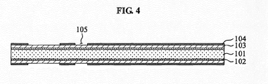
- a base layer 103' formed as an aluminum foil having a predetermined thickness is prepared.
- soft etching may be performed on a surface of the base layer 103' using a sulfuric acid type, or oxidation treatment may be performed to form surface roughness of the base layer 103'.
- a base layer 103 on which the surface roughness is formed is bonded onto both an upper face and a lower face of an insulation layer 101 of an insulating material using a bonding member 102.
- a bonding member 102 For example, a polyimide-based insulating bonding sheet, which is a binder having a desirable bonding performance and insulating function, or an epoxy type such as glass epoxy resin may be used for the bonding member 102.
- a material having a thermal expansion coefficient similar to a thermal expansion coefficient of the base layer 103 may be used for the bonding member 102.
- the polyimide since polyimide endures at a high temperature of 400 °C or above or at a low temperature of -269 °C, the polyimide may absorb a change rate based on a thermal expansion coefficient of aluminum, for example, 23.03 x 10⁻⁶ °C.
- a predetermined temperature and pressure may be applied to the base layer 103.
- a dry film 104 is applied onto the base layer 103.
- a pattern 105 is formed through light exposure and development for a predetermined amount of time.
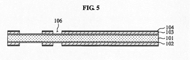
- a circuit pattern 106 is formed by removing the base layer 103 based on the pattern 105 of the dry film 104.
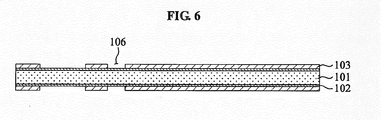
- a PCB is formed by removing the dry film 104 from the base layer 103 on which the circuit pattern 106 is formed.
- the circuit pattern 106 is formed by selectively removing a portion of the base layer 103 exposed by the pattern 105 using hydrochloric acid-based acidic etching in a state in which the dry film 104 is connected to the base layer 103.
- a hydrochloric acid type for example, ferric chloride, cupric chloride, and sodium chlorate, may be used.
- circuit pattern 106 may be formed directly on the base layer 103 as an example, the present invention may not be limited thereto. Alternatively, the circuit pattern 106 may be formed on a plating layer after the plating layer is formed on the base layer 103 using electrolytic or electroless plating.
- circuit pattern 106 Although a chemical method used to form the circuit pattern 106 is illustrated as an example, the present invention may not be limited thereto. Alternatively, a mechanical method using punching and the like may be used to form the circuit pattern 106. Alternatively, only a through hole may be formed to connect an electrode or a metal layer in lieu of the circuit pattern 106.
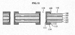
- FIGS. 7 through 12 are mimetic diagrams illustrating a method of manufacturing a multilayer PCB using the PCB manufactured in accordance with the method described with reference to FIGS. 1 through 6 .
- the PCB manufactured in accordance with the method described with reference to FIGS. 1 through 6 will be referred to as a double-sided substrate.
- an insulation layer 107 having a predetermined thickness is formed to fill the circuit pattern 106 in the double-sided substrate manufactured in accordance with the method described with reference to FIGS. 1 through 6 .
- a base layer 109 is bonded onto the insulation layer 107 using a bonding member 108.
- the base layer 109 may be an aluminum foil having a predetermined thickness.
- a polyimide-based insulating bonding sheet or an epoxy type may be used for the bonding member 108.
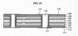
- a via hole 110 is formed to penetrate all the double-sided substrate, the insulation layer 107, the bonding member 108, and the base layer 109.
- the via hole 110 may be formed by drilling or laser processing.
- a metal layer 111 is formed to metalize a cross-sectional portion of the insulation layers 101 and 107 and the bonding members 102 and 108, which is exposed to an inner side of the via hole 110.
- the metal layer 111 may form a carbon plating layer using carbon direct plating. With the formation of the metal layer 111, the base layers 103 and 109 are electrically connected.
- a substitution layer 112 having a predetermined thickness is formed by performing zincate treatment on a surface of the base layer 109 from which the metal layer 111 is excluded.
- the substitution layer 112 is formed by a portion of the surface of the base layer 109 being substituted by a zinc film.
- the thickness of the substitution layer 112 is formed to be equal to a thickness of the meal layer 111 based on the thickness of the metal layer 111.
- the substitution layer 112 having the thickness is formed on a remaining surface of the base layer 109 from which the metal layer 111 is excluded.
- aluminum may be prevented from being oxidized in an atmosphere and thus, the surface of the base layer 109 may be protected.
- the surface of the base layer 109 being substituted by the zinc film, the surface of the base layer 109 may be prevented from being corroded during electrolytic and electroless plating to be subsequently performed.
- a substitution plating layer 113 is formed on the substitution layer 112 using the electrolytic or the electroless plating.
- the substitution plating layer 113 is formed on the substitution layer 112 by performing displacement plating using a metal film having a strong chemical resistance.
- the substitution plating layer 113 may be formed by performing the displacement plating using nickel (Ni) and substituting a nickel film for the substitution layer 112.
- the displacement plating may not be limited to using nickel.
- other metals having a strong chemical resistance for example, gold (Au) and silver (Ag), may be used for the displacement plating.
- substitution layer 112 may not be limited thereto.
- a case in which both the metal layer 111 and the substitution layer 112 are substituted by the substitution plating layer 113 may be considered.
- the substitution plating layer 113 may be formed only on the substitution layer 112 apart from the metal layer 111, or formed to cover a portion or an entirety of the metal layer 111.
- An electrolytic plating layer 114 is formed on the substitution plating layer 113.
- the electrolytic plating layer 114 is formed also on the substitution plating layer 113 in the via hole 110.
- the electrolytic plating layer 114 may be a copper film through copper plating.
- the electrolytic plating layer 114 is formed using the electrolytic plating.
- the electrolytic plating layer 114 may be formed to have a thickness of greater than or equal to 20 micrometers ( ⁇ m).
- the substitution plating layer 113 and the electrolytic plating layer 114 is formed on a surface of the metal layer 111.
- the electrolytic plating layer 114 is formed to cover all the substitution plating layer 113 and the metal layer 111, and only the electrolytic plating layer 114 is formed on the metal layer 111.
- the substitution plating layer 113 is formed to cover a portion of the metal layer 111
- the electrolytic plating layer 114 is formed to cover all the substitution plating layer 113 and the metal layer 111.
- the electrolytic plating layer 114 covers the substitution plating layer 113 and thus, two layers, the substitution plating layer 113 and the electrolytic plating layer 114, are formed on the metal layer 111.
- a pattern 116 is formed by applying a dry film 115 onto the electrolytic plating layer 114 and performing light exposure and development for a predetermined amount of time.
- a circuit pattern 117 is formed by removing the electrolytic plating layer 114, the substitution plating layer 113, the substitution layer 112, and the base layer 109 using the dry film 115 on which the pattern 116 is formed.
- the circuit pattern 117 is formed by removing the electrolytic plating layer 114, the substitution plating layer 113, the substitution layer 112, and up to the base layer 109 through hydrochloric acid-based acidic etching using the dry film 115.
- a multilayer PCB for example, triple or more layered substrate, may be formed by repetitively performing operations described with reference to FIGS. 7 through 11 .
- a higher multiple layered PCB may be formed by layering at least three double-sided substrates through operations to be described with reference to FIG. 12 .
- FIG. 12 illustrates a multilayer PCB formed by layering at least two double-sided substrates manufactured through the method described with reference to FIGS. 1 through 6 .
- an insulation layer 107 is interposed between the double-sided substrates to be layered to electrically separate the double-sided substrates.
- the insulation layer 107, a bonding member 108, and a base layer 109 are formed on each of an uppermost face and a lowermost face of the double-sided substrates.
- a via hole is formed, and then the metal layer 111, the substitution layer 112, the substitution plating layer 113, and the electrolytic plating layer 114 are sequentially formed.
- a high multiple layer substrate which is the multilayer PCB, is formed by forming the circuit pattern 117 using the dry film 115.
- the circuit pattern 117 is formed through a chemical method using the hydrochloric acid-based acidic etching using the dry film 115.
- the chemical method may be used to form the circuit pattern 117 by selectively removing a layer, for example, removing up to the second base layer 109 in addition to the electrolytic plating layer 114, the substitution plating layer 113, and the substitution layer 112.
- a mechanical method using punching and the like may be used to form a pattern on a base layer to be layered in the high multiple layer substrate. Further, only a through hole may be formed to connect an electrode or a metal layer in a predetermined form.
- a PCB manufactured in accordance with example embodiments described herein may be applicable to an electronic component for a vehicle.
Landscapes
- Engineering & Computer Science (AREA)
- Chemical & Material Sciences (AREA)
- Microelectronics & Electronic Packaging (AREA)
- Manufacturing & Machinery (AREA)
- Materials Engineering (AREA)
- Metallurgy (AREA)
- Organic Chemistry (AREA)
- Chemical Kinetics & Catalysis (AREA)
- Mechanical Engineering (AREA)
- General Chemical & Material Sciences (AREA)
- Electrochemistry (AREA)
- Physics & Mathematics (AREA)
- Thermal Sciences (AREA)
- Manufacturing Of Printed Wiring (AREA)
- Insulated Metal Substrates For Printed Circuits (AREA)
- Production Of Multi-Layered Print Wiring Board (AREA)
- Printing Elements For Providing Electric Connections Between Printed Circuits (AREA)
Applications Claiming Priority (2)
| Application Number | Priority Date | Filing Date | Title |
|---|---|---|---|
| KR1020120141576A KR20140073757A (ko) | 2012-12-07 | 2012-12-07 | 인쇄회로기판 및 그 제조방법 |
| PCT/KR2013/011247 WO2014088357A1 (ko) | 2012-12-07 | 2013-12-06 | 인쇄회로기판 및 그 제조방법 |
Publications (2)
| Publication Number | Publication Date |
|---|---|
| EP2931008A1 true EP2931008A1 (de) | 2015-10-14 |
| EP2931008A4 EP2931008A4 (de) | 2016-08-17 |
Family
ID=50883711
Family Applications (1)
| Application Number | Title | Priority Date | Filing Date |
|---|---|---|---|
| EP13861374.0A Withdrawn EP2931008A4 (de) | 2012-12-07 | 2013-12-06 | Leiterplatte und herstellungsverfahren dafür |
Country Status (5)
| Country | Link |
|---|---|
| US (1) | US9769921B2 (de) |
| EP (1) | EP2931008A4 (de) |
| KR (2) | KR20140073757A (de) |
| CN (1) | CN105103663A (de) |
| WO (1) | WO2014088357A1 (de) |
Families Citing this family (9)
| Publication number | Priority date | Publication date | Assignee | Title |
|---|---|---|---|---|
| JP2014216375A (ja) * | 2013-04-23 | 2014-11-17 | イビデン株式会社 | プリント配線板及び多層コア基板の製造方法 |
| JP2016072334A (ja) * | 2014-09-29 | 2016-05-09 | 日本ゼオン株式会社 | 積層体の製造方法 |
| US10211071B2 (en) * | 2016-01-29 | 2019-02-19 | Nxp B.V. | IC packaging method and a packaged IC device |
| KR102400748B1 (ko) * | 2017-09-12 | 2022-05-24 | 삼성전자 주식회사 | 인터포저를 포함하는 전자 장치 |
| KR20190041215A (ko) * | 2017-10-12 | 2019-04-22 | 주식회사 아모그린텍 | 인쇄회로기판 제조 방법 및 이에 의해 제조된 인쇄회로기판 |
| KR102465117B1 (ko) * | 2017-11-29 | 2022-11-11 | 주식회사 잉크테크 | 인쇄회로기판 제조방법 |
| CN110859029B (zh) | 2018-08-23 | 2022-04-01 | 鹏鼎控股(深圳)股份有限公司 | 柔性电路板及该柔性电路板制作方法 |
| JP2021027167A (ja) * | 2019-08-05 | 2021-02-22 | イビデン株式会社 | 配線基板 |
| CN111586993B (zh) * | 2020-05-19 | 2023-06-20 | 陕西凌云电器集团有限公司 | 一种回流焊接孔金属化的铝基微带板生产工艺 |
Family Cites Families (11)
| Publication number | Priority date | Publication date | Assignee | Title |
|---|---|---|---|---|
| JP3165617B2 (ja) * | 1995-03-27 | 2001-05-14 | シャープ株式会社 | 多層プリント配線基板及びその製造方法 |
| TW532050B (en) * | 2000-11-09 | 2003-05-11 | Matsushita Electric Industrial Co Ltd | Circuit board and method for manufacturing the same |
| JP2004179291A (ja) | 2002-11-26 | 2004-06-24 | Ibiden Co Ltd | 配線板および配線板の製造方法 |
| US20050178669A1 (en) * | 2004-02-17 | 2005-08-18 | Strubbe John L. | Method of electroplating aluminum |
| JP4327774B2 (ja) * | 2005-07-21 | 2009-09-09 | 富士ネームプレート株式会社 | プリント配線板及びその製造方法 |
| KR100674321B1 (ko) | 2005-09-02 | 2007-01-24 | 삼성전기주식회사 | 방열특성이 향상된 인쇄회로기판 및 그 제조방법 |
| JP5101919B2 (ja) * | 2007-04-09 | 2012-12-19 | 日東電工株式会社 | 配線回路基板用両面粘着テープ又はシートおよび両面粘着テープ付き配線回路基板 |
| KR20090053628A (ko) * | 2007-11-23 | 2009-05-27 | 삼성전기주식회사 | 인쇄회로기판 및 그 제조방법 |
| KR100950916B1 (ko) * | 2008-05-06 | 2010-04-01 | 삼성전기주식회사 | 인쇄회로기판의 제조방법 및 이에 의해 제조된인쇄회로기판 |
| JP4605409B2 (ja) * | 2008-08-21 | 2011-01-05 | 上村工業株式会社 | アルミニウム又はアルミニウム合金の表面処理方法 |
| KR101077340B1 (ko) | 2009-12-15 | 2011-10-26 | 삼성전기주식회사 | 기판 제조용 캐리어 부재 및 이를 이용한 기판의 제조방법 |
-
2012
- 2012-12-07 KR KR1020120141576A patent/KR20140073757A/ko active Pending
-
2013
- 2013-12-06 EP EP13861374.0A patent/EP2931008A4/de not_active Withdrawn
- 2013-12-06 CN CN201380063632.6A patent/CN105103663A/zh active Pending
- 2013-12-06 WO PCT/KR2013/011247 patent/WO2014088357A1/ko not_active Ceased
- 2013-12-06 KR KR1020137032719A patent/KR20150094794A/ko not_active Abandoned
-
2015
- 2015-06-05 US US14/732,309 patent/US9769921B2/en not_active Expired - Fee Related
Also Published As
| Publication number | Publication date |
|---|---|
| WO2014088357A1 (ko) | 2014-06-12 |
| US9769921B2 (en) | 2017-09-19 |
| CN105103663A (zh) | 2015-11-25 |
| US20150271917A1 (en) | 2015-09-24 |
| KR20140073757A (ko) | 2014-06-17 |
| EP2931008A4 (de) | 2016-08-17 |
| KR20150094794A (ko) | 2015-08-20 |
Similar Documents
| Publication | Publication Date | Title |
|---|---|---|
| EP2931008A1 (de) | Leiterplatte und herstellungsverfahren dafür | |
| KR100969412B1 (ko) | 다층 인쇄회로기판 및 그 제조방법 | |
| KR20060105412A (ko) | 양면 배선 보드 제조 방법, 양면 배선 보드 및 그 기재 | |
| US9788421B2 (en) | Printed circuit board and method of manufacturing same | |
| US9510446B2 (en) | Printed circuit board and manufacture method thereof | |
| EP2931010A1 (de) | Leiterplatte | |
| JP2009010266A (ja) | プリント配線板の製造方法及びプリント配線板 | |
| EP3039948A1 (de) | Verfahren zur herstellung einer flexiblen leiterplatte und eine flexible leiterplatte | |
| KR101854626B1 (ko) | 인쇄회로기판의 제조방법 및 그에 따라서 제조된 인쇄회로기판 | |
| JP4747569B2 (ja) | 固体電解コンデンサ内蔵基板の製造方法 | |
| CN104105334B (zh) | 印刷电路板及其制造方法 | |
| CN109950017B (zh) | 电子部件以及电子部件的制造方法 | |
| CN201336772Y (zh) | 多层布线板 | |
| KR101927479B1 (ko) | 인쇄회로기판 제조방법 및 그에 따라서 제조된 인쇄회로기판 | |
| JP2007281111A (ja) | 固体電解コンデンサおよび固体電解コンデンサ内蔵基板と、それらの製造方法 | |
| JP2009141298A (ja) | 多層配線板及びその製造方法 | |
| JP2008166456A (ja) | 配線基板及びその製造方法 | |
| JP2003060354A (ja) | 部品内蔵プリント回路板及びその製造方法 | |
| JP2005153298A (ja) | 両面銅張積層板及びその製造方法並びに多層積層板 | |
| JP2003031943A (ja) | 多層配線基板及びその製造方法 |
Legal Events
| Date | Code | Title | Description |
|---|---|---|---|
| PUAI | Public reference made under article 153(3) epc to a published international application that has entered the european phase |
Free format text: ORIGINAL CODE: 0009012 |
|
| 17P | Request for examination filed |
Effective date: 20150629 |
|
| AK | Designated contracting states |
Kind code of ref document: A1 Designated state(s): AL AT BE BG CH CY CZ DE DK EE ES FI FR GB GR HR HU IE IS IT LI LT LU LV MC MK MT NL NO PL PT RO RS SE SI SK SM TR |
|
| AX | Request for extension of the european patent |
Extension state: BA ME |
|
| RIN1 | Information on inventor provided before grant (corrected) |
Inventor name: BEAK, OK KY Inventor name: CHOI, YANG YOON |
|
| DAX | Request for extension of the european patent (deleted) | ||
| RA4 | Supplementary search report drawn up and despatched (corrected) |
Effective date: 20160714 |
|
| RIC1 | Information provided on ipc code assigned before grant |
Ipc: H05K 1/09 20060101AFI20160708BHEP Ipc: H05K 7/20 20060101ALI20160708BHEP Ipc: H05K 3/46 20060101ALI20160708BHEP |
|
| RAP1 | Party data changed (applicant data changed or rights of an application transferred) |
Owner name: TYCO ELECTRONICS AMP KOREA CO., LTD. |
|
| 17Q | First examination report despatched |
Effective date: 20191118 |
|
| STAA | Information on the status of an ep patent application or granted ep patent |
Free format text: STATUS: THE APPLICATION HAS BEEN WITHDRAWN |
|
| 18W | Application withdrawn |
Effective date: 20200130 |