EP2930552A2 - Anzeigevorrichtung und optische Vorrichtung - Google Patents
Anzeigevorrichtung und optische Vorrichtung Download PDFInfo
- Publication number
- EP2930552A2 EP2930552A2 EP15152708.2A EP15152708A EP2930552A2 EP 2930552 A2 EP2930552 A2 EP 2930552A2 EP 15152708 A EP15152708 A EP 15152708A EP 2930552 A2 EP2930552 A2 EP 2930552A2
- Authority
- EP
- European Patent Office
- Prior art keywords
- light
- light guide
- image
- dimming
- frame
- Prior art date
- Legal status (The legal status is an assumption and is not a legal conclusion. Google has not performed a legal analysis and makes no representation as to the accuracy of the status listed.)
- Granted
Links
Images


Classifications
-
- G—PHYSICS
- G02—OPTICS
- G02B—OPTICAL ELEMENTS, SYSTEMS OR APPARATUS
- G02B27/00—Optical systems or apparatus not provided for by any of the groups G02B1/00 - G02B26/00, G02B30/00
- G02B27/01—Head-up displays
- G02B27/017—Head mounted
- G02B27/0172—Head mounted characterised by optical features
-
- G—PHYSICS
- G02—OPTICS
- G02B—OPTICAL ELEMENTS, SYSTEMS OR APPARATUS
- G02B27/00—Optical systems or apparatus not provided for by any of the groups G02B1/00 - G02B26/00, G02B30/00
- G02B27/01—Head-up displays
- G02B27/0101—Head-up displays characterised by optical features
-
- G—PHYSICS
- G02—OPTICS
- G02B—OPTICAL ELEMENTS, SYSTEMS OR APPARATUS
- G02B23/00—Telescopes, e.g. binoculars; Periscopes; Instruments for viewing the inside of hollow bodies; Viewfinders; Optical aiming or sighting devices
- G02B23/14—Viewfinders
-
- G—PHYSICS
- G02—OPTICS
- G02B—OPTICAL ELEMENTS, SYSTEMS OR APPARATUS
- G02B27/00—Optical systems or apparatus not provided for by any of the groups G02B1/00 - G02B26/00, G02B30/00
- G02B27/01—Head-up displays
- G02B27/017—Head mounted
-
- G—PHYSICS
- G02—OPTICS
- G02B—OPTICAL ELEMENTS, SYSTEMS OR APPARATUS
- G02B5/00—Optical elements other than lenses
- G02B5/32—Holograms used as optical elements
-
- G—PHYSICS
- G02—OPTICS
- G02B—OPTICAL ELEMENTS, SYSTEMS OR APPARATUS
- G02B6/00—Light guides; Structural details of arrangements comprising light guides and other optical elements, e.g. couplings
- G02B6/0001—Light guides; Structural details of arrangements comprising light guides and other optical elements, e.g. couplings specially adapted for lighting devices or systems
- G02B6/0011—Light guides; Structural details of arrangements comprising light guides and other optical elements, e.g. couplings specially adapted for lighting devices or systems the light guides being planar or of plate-like form
-
- G—PHYSICS
- G09—EDUCATION; CRYPTOGRAPHY; DISPLAY; ADVERTISING; SEALS
- G09G—ARRANGEMENTS OR CIRCUITS FOR CONTROL OF INDICATING DEVICES USING STATIC MEANS TO PRESENT VARIABLE INFORMATION
- G09G5/00—Control arrangements or circuits for visual indicators common to cathode-ray tube indicators and other visual indicators
- G09G5/10—Intensity circuits
-
- G—PHYSICS
- G02—OPTICS
- G02B—OPTICAL ELEMENTS, SYSTEMS OR APPARATUS
- G02B27/00—Optical systems or apparatus not provided for by any of the groups G02B1/00 - G02B26/00, G02B30/00
- G02B27/01—Head-up displays
- G02B27/0101—Head-up displays characterised by optical features
- G02B2027/0118—Head-up displays characterised by optical features comprising devices for improving the contrast of the display / brillance control visibility
-
- G—PHYSICS
- G02—OPTICS
- G02B—OPTICAL ELEMENTS, SYSTEMS OR APPARATUS
- G02B27/00—Optical systems or apparatus not provided for by any of the groups G02B1/00 - G02B26/00, G02B30/00
- G02B27/01—Head-up displays
- G02B27/0101—Head-up displays characterised by optical features
- G02B2027/0132—Head-up displays characterised by optical features comprising binocular systems
-
- G—PHYSICS
- G02—OPTICS
- G02B—OPTICAL ELEMENTS, SYSTEMS OR APPARATUS
- G02B27/00—Optical systems or apparatus not provided for by any of the groups G02B1/00 - G02B26/00, G02B30/00
- G02B27/01—Head-up displays
- G02B27/017—Head mounted
- G02B2027/0178—Eyeglass type
-
- G—PHYSICS
- G02—OPTICS
- G02B—OPTICAL ELEMENTS, SYSTEMS OR APPARATUS
- G02B27/00—Optical systems or apparatus not provided for by any of the groups G02B1/00 - G02B26/00, G02B30/00
- G02B27/10—Beam splitting or combining systems
- G02B27/14—Beam splitting or combining systems operating by reflection only
- G02B27/144—Beam splitting or combining systems operating by reflection only using partially transparent surfaces without spectral selectivity
-
- G—PHYSICS
- G09—EDUCATION; CRYPTOGRAPHY; DISPLAY; ADVERTISING; SEALS
- G09G—ARRANGEMENTS OR CIRCUITS FOR CONTROL OF INDICATING DEVICES USING STATIC MEANS TO PRESENT VARIABLE INFORMATION
- G09G2320/00—Control of display operating conditions
- G09G2320/06—Adjustment of display parameters
- G09G2320/0626—Adjustment of display parameters for control of overall brightness
-
- G—PHYSICS
- G09—EDUCATION; CRYPTOGRAPHY; DISPLAY; ADVERTISING; SEALS
- G09G—ARRANGEMENTS OR CIRCUITS FOR CONTROL OF INDICATING DEVICES USING STATIC MEANS TO PRESENT VARIABLE INFORMATION
- G09G2360/00—Aspects of the architecture of display systems
- G09G2360/14—Detecting light within display terminals, e.g. using a single or a plurality of photosensors
- G09G2360/144—Detecting light within display terminals, e.g. using a single or a plurality of photosensors the light being ambient light
Definitions
- a display apparatus used as a head mounted display is publicly known based on Japanese Patent Application Laid-open No. 2006-209144 , for example.
- This display apparatus in the form of eyeglasses includes, on temples thereof, a reception unit configured to receive an image singal transmitted from an image information transmission source, a drive unit configured to decode the image singal received in the reception unit, a display unit configured to display an image obtained by decoding in the drive unit, and a power supply unit configured to supply power to the reception unit, the drive unit, and the display unit.
- the display unit includes a display including an image output device, an optical member, and a Lippman-Bragg volume hologram sheet.
- this allows the observer to easily and reliably recognize that an image is to be displayed.
- a spatial area imaged by the imaging device is displayed on the dimming device. This allows the observer to easily, reliably, and immediately recognize which part of the outside is imaged by the imaging device.
- light transmittance of the dimming device is changed based on a signal received by the receiving device. This allows the observer to easily, reliably, and immediately recognize that the receiving device receives a signal.
- the display apparatus including the various desirable forms described above may further include a sensor configured to measure the brightness in the outside environment, and light transmittance of a partial area of the dimming device may be changed based on a measurement result of the brightness in the outside environment obtained by the sensor.
- the sensor may be formed of a well-known illumination sensor, and the control of the sensor may be performed based on a well-known control circuit provided to the image display device.
- Each of the optical apparatuses according to the first and second embodiments of the present disclosure may also include a sensor configured to measure the brightness in the outside environment, and light transmittance of a partial area of the dimming device may be changed based on a measurement result of the brightness in the outside environment obtained by the sensor.
- the outer edge of a spatial area imaged by an imaging device may be displayed in the form of a frame in the dimming device.
- light transmittance of an area of the dimming device that corresponds to the spatial area imaged by the imaging device may be made lower than light transmittance of an area of the dimming device that corresponds to the outside of the spatial area imaged by the imaging device.
- the observer sees the spatial area imaged by the imaging device as an area darker than the outside of the spatial area imaged by the imaging device.
- the light-transmission control material layer may be an optical shutter formed of a liquid crystal material layer, or may be an optical shutter formed of an inorganic EL (electroluminescence) material layer.
- the optical shutter for use in the dimming device may also be an optical shutter configured by an electrophoretic dispersion liquid including a large number of electrically-charged electrophoretic particles and a dispersion medium colored differently from the electrophoretic particles, an optical shutter configured by application of electrodeposition/dissociation that occurs in response to the reversible oxidation reduction of metal, e.g., silver particles, an optical shutter configured by utilizing color change of substance that occurs in response to the oxidation reduction of an electrochromic material, or an optical shutter configured by controlling the light transmittance by electrowetting.
- the dimming device may be detachably disposed.
- the dimming device may be attached to the frame by using a screw made of transparent plastic, by forming a groove to the frame for engagement of the dimming device, or by providing a magnet to the frame.
- the frame may be also provided with a slide section to slide the dimming device thereinto.
- the dimming device may be provided with a connector for electrical connection to a control circuit via this connector and a wire. This control circuit is for controlling the light transmittance of the dimming device, and is provided in the control device for controlling the image forming unit, for example.
- the dimming device may be bent.
- the light shielding member may be provided to the light guide unit on the side not provided with the image forming unit, and is provided with a distance from the light guide unit.
- the light shielding member may be made of a non-transparent plastic material, for example.
- Such a light shielding member may be integrally extended from the casing of the image display device or may be attached to the casing of the image display device.
- the light shielding member may be integrally extended from the frame or may be attached to the frame.
- the light shielding member may be disposed at a portion of the light guide unit, on the side not provided with the image forming unit, or may be provided to the dimming device.
- the amount of outside light that passes through the dimming device when the dimming device does not operate when the amount of outside light that passes through the dimming device when the dimming device does not operate is assumed to be "1", the amount of outside light that passes through the dimming device when the dimming device is operating may be assumed to be in the range from 0.3 to 0.8, desirably, 0.5 to 0.8. This allows the observer to easily, reliably, and immediately recognize that an image is displayed. Alternatively, this allows the observer to easily and reliably recognize that an image is to be displayed.
- each of the first deflection unit and the second deflection unit may be formed of a laminate of P diffraction grating layers formed of the diffraction grating members.
- an interference fringe corresponding to one type of wavelength band (or wavelength) is formed.
- the diffraction grating member formed of one diffraction grating layer may also be provided with P types of interference fringes.
- an interference fringe is formed inside and over the surface of the diffraction grating member
- a method of forming the interference fringe may be the same as a forming method in related art.
- object light may be applied to a member (for example, photopolymer material) that forms a diffraction grating member from a first predetermined direction on one side
- reference light may be applied to the member that forms the diffraction grating member from a second predetermined direction on the other side at the same time, to record an interference fringe formed by the object light and the reference light in the member that forms the diffraction grating member.
- each of the first diffraction grating member and the second diffraction grating member is formed of a laminate structure of the P diffraction grating layers formed of the reflective volume holographic diffraction gratings
- P diffraction grating layers in order to laminate such diffraction grating layers, P diffraction grating layers only need to be independently produced and then laminated on (bonded to) each other with use of an ultraviolet curable adhesive, for example.
- P diffraction grating layers may be produced by producing one diffraction grating layer with use of a photopolymer material having viscosity and then sequentially attaching the photopolymer materials having viscosity thereto, to produce the diffraction grating layer.
- the image forming unit may include a plurality of pixels arranged in a two-dimensional matrix. It should be noted that the image forming unit having such a configuration is referred to as an "image forming unit having a first configuration" for convenience sake.
- Examples of the image forming unit having a first configuration include: an image forming unit including a reflective spatial light modulation device and a light source; an image forming unit including a transmissive spatial light modulation device and a light source; and an image forming unit including a light-emitting element such as a light-emitting diode (LED), a semiconductor laser element, an organic EL (Electro Luminescence) element, or an inorganic EL element.
- LED light-emitting diode
- LED light-emitting diode
- LED light-emitting diode
- semiconductor laser element a semiconductor laser element
- organic EL (Electro Luminescence) element an organic EL (Electro Luminescence) element
- the two image display devices are connected to each other with the connection member, and specifically, the following form can be adopted: two light guide plates are connected to each other with the connection member.
- the connection member is attached to such a light guide plate integrally produced.
- Such a form is also included in the form in which the two light guide plates are connected to each other with the connection member.
- the light guide plate has two parallel surfaces (first surface and second surface) extending parallel to the axis of the light guide plate (the axis corresponds to a longitudinal direction or horizontal direction and corresponds to the X axis). It should be noted that the width direction of the light guide plate, which corresponds to a height direction or a vertical direction, corresponds to a Y axis. Assuming that a surface of the light guide plate, to which light is input, is an input surface of the light guide plate, and a surface of the light guide plate, from which light is output, is an output surface of the light guide plate, the input surface of the light guide plate and the output surface of the light guide plate may be each formed of the first surface. Alternatively, the input surface of the light guide plate may be formed of the first surface, and the output surface of the light guide plate may be formed of the second surface.
- the interference fringe of the diffraction grating member extends substantially parallel to the Y axis.
- each image forming unit includes a headphone portion and a headphone portion wire, which extends from each image forming unit, is extended from the tip end of the earpiece portion to the headphone portion through the inside of the temple portion and the earpiece portion.
- Examples of the headphone portion may include an inner ear type headphone portion and a canal type headphone portion. More specifically, it is desirable to adopt a form in which the headphone portion wire is extended to the headphone portion so as to run around the rear side of a pinna (auricle) from the tip end of the earpiece portion.
- a pinna auricle
- the frame may include a front portion disposed on the front of the observer, and two temple portions turnably attached to both ends of the front portion via hinges. It should be noted that the earpiece portions are attached to the tip ends of the respective temple portions.
- the dimming device is attached to the frame. Specifically, for example, the dimming device only needs to be attached to the front portion. Further, a configuration in which the front portion and the two temple portions are incorporated can be adopted. In other words, when the whole of the optical apparatus according to each of the first and second embodiments of the present disclosure is viewed, generally, the frame has substantially the same structure as that of normal eyeglasses.
- the dimming device is disposed instead of the lenses of the normal eyeglasses.
- the materials forming the frame may be the same as materials forming normal eyeglasses, such as metals, alloys, plastics, and combinations thereof.
- a configuration in which nose pads are attached to the front portion can be adopted.
- an assembled body of the frame and the nose pads has substantially the same structure as that of normal eyeglasses, except for the absence of a rim.
- the nose pads can have a well-known configuration and structure.
- the imaging device may be an imaging device having a well-known configuration and structure.
- the imaging device may include a solid-state imaging device, which has a CCD (Charge Coupled Device) or a CMOS (Complementary Metal Oxide Semiconductor) sensor, and a lens, for example.
- CCD Charge Coupled Device
- CMOS Complementary Metal Oxide Semiconductor
- the imaging device may be attached to the central part or end of the front portion or to the temple portion. Wires from the imaging device may be connected to one image display device (or image forming unit) via the front portion, for example, or may be included in the wires extending from the image display device (or image forming unit).
- a spatial area imaged by the imaging device may be displayed on the dimming device.
- the luminance data in use corresponds to the luminance at a predetermined area including an observation target viewed through the image display device
- the luminance data may be adjusted in value to increase the luminance of an image to be displayed, i.e., to make the image brighter when it is displayed, if the luminance at the predetermined area including the observation target viewed through the image display device is increased.
- the chromaticity data in use corresponds to the chromaticity at the predetermined area including the observation target viewed through the image display device
- the chromaticity data may be adjusted in value to obtain, roughly, a complementary color relationship between the chromaticity at the predetermined area including the observation target viewed through the image display device and the chromaticity of an image to be displayed.
- the complementary colors mean a pair of colors that are opposite to each other on the color circle, e.g., red and green, yellow and purple, and blue and orange.
- the complementary colors also mean a pair of colors that produces a color with reduced chroma when mixed in appropriate proportions, e.g., white for light, and black for objects.
- the complementary characteristics are not the same in terms of visual effects when the colors are placed next to each other, and when the colors are mixed together.
- the complementary colors are also referred to as antagonistic colors, contrast colors, or opposing colors. It should be noted that the expression of "opposing colors” directly identifies which colors are opposite to each other, whereas the expression of "complementary colors” identifies colors in a rather wider scope.
- the pair of complementary colors produces synergistic effects of enhancing their respective colors, and this is called complementary color harmony.
- Embodiment 1 relates to the display apparatus according to the embodiment of the present disclosure, and to the optical apparatus according to the second embodiment of the present disclosure.
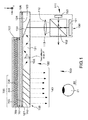
- Fig. 1 is a conceptual diagram of an image display device of Embodiment 1.
- Fig. 2 is a schematic diagram of the display apparatus (specifically, head mounted display (HMD)) of Embodiment 1 and the like when viewed from above.
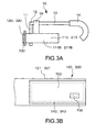
- Fig. 3A is a schematic diagram of the display apparatus of Embodiment 1 when viewed from a lateral direction.
- Fig. 3B is a schematic diagram of a part including a light guide unit and a dimming device in the display apparatus of Embodiment 1 when viewed from the front.
- the display apparatus of Embodiment 1 or Embodiments 2 to 14 that will be described later is a head mounted display (HMD) including
- the optical apparatus of Embodiment 1 or Embodiments 2 to 14 that will be described later includes
- the receiving device can receive the signals.
- the display apparatus receives a signal for displaying an image on the image display device 100, 200, 300, 400, or 500, e.g., electronic mails and various types of information in a variety of sites on the Internet
- the light transmittance of the partial area 708 of the dimming device 700 is changed under the control of the control device 18, before the electronic mails and various types of information in a variety of sites on the Internet are displayed on the image display device 100, 200, 300, 400, or 500.
- the signals for displaying images on the image display device 100, 200, 300, 400, or 500 may be stored in the image display device, e.g., specifically in an image information storage unit 18A in the control device 18, and before images are displayed on the image display device 100, 200, 300, 400, or 500, the light transmittance of the partial area 708 of the dimming device 700 is changed under the control of the control device 18. Alternatively, the light transmittance of the dimming device 700 is changed based on the signal received by the receiving device.
- the amount of outside light that passes through the dimming device 700 when the dimming device 700 does not operate is assumed to be "1"
- Each of the image display devices 100, 200, 300, 400, and 500 of Embodiment 1 and Embodiments 2 to 14 that will be described later includes
- the image display device 100, 200, 300, 400, or 500 may be attached to the frame in a fixed manner or detachably.
- the optical system 112 or 254 is disposed between the image forming unit 111 or 211 and the light guide unit 120, 320, or 520.
- the light flux changed into the parallel light in the optical system 112 or 254 is input to the light guide unit 120, 320, or 520, guided therethrough, and output therefrom.
- the light guide unit 120, 320, or 520 is semi-transmissive (see-through). Specifically, portions of the light guide units, which are opposed to at least the both eyes of the observer 20 (more specifically, light guide plate 121 or 321 and second deflection unit 140 or 340 that will be described later), are semi-transmissive (see-through).
- Each of the light guide units 120 and 320 in Embodiment 1 and Embodiments 2 to 4 and 6 to 14 that will be described later includes
- the first deflection unit 130 and the second deflection unit 140 are disposed inside the light guide plate 121.
- the first deflection unit 130 reflects light input to the light guide plate 121
- the second deflection unit 140 transmits and reflects the light a plurality of times, the light being propagated inside the light guide plate 121 by total reflection.
- the first deflection unit 130 functions as a reflecting mirror
- the second deflection unit 140 functions as a semi-transmissive mirror.
- the first deflection unit 130 provided inside the light guide plate 121 is made of aluminum (Al) and is formed of a light reflecting film (a kind of mirror) that reflects the light input to the light guide plate 121.
- the second deflection unit 140 provided inside the light guide plate 121 is formed of a multi-layer lamination structure in which many dielectric lamination films are laminated.
- the dielectric lamination films includes a layer of TiO 2 (titanium dioxide) being a high dielectric material, and a layer of SiO 2 (silicon dioxide) being a low dielectric material, for example.
- TiO 2 titanium dioxide
- SiO 2 silicon dioxide
- the multi-layer lamination structure in which many dielectric lamination films are laminated is described in Japanese Unexamined Patent Application Publication No. 2005-521099 .
- Six dielectric lamination films are exemplarily shown in the figures, but this is not restrictive.
- a dielectric lamination film and another dielectric lamination film include therebetween a very thin layer made of the same material as the light guide plate 121.
- each headphone portion wire 16' is extended to the headphone portion 16 so as to run around the rear side of a pinna (auricle) from the tip end of the earpiece portion 14.
- a pinna auricle
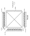
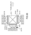
- the two substrates 701 and 703 are sealed together at outer edge portions using a sealing agent 706.
- the first substrate 701 of the dimming device 700 and the protection member 126 (protecting the light guide plate 121) are bonded to each other by the adhesive 707. Further, polarizer films are affixed to the outer surfaces of the first substrate 701 and the second substrate 703, but those polarizer films are not shown.
- the first substrate 701 in the dimming device 700 is shorter than the light guide plate 121, and the first substrate 701 in the dimming device 700 is fixed to the protection member 126 using the adhesive 707.
- the adhesive 707 is provided at the outer edge portion of the first substrate 701. This is applicable also to other Embodiments to be described below.
- the light guide unit 120 and the dimming device 700 are disposed in this order from the observer's side.
- the light transmittance of the dimming device 700 may be controlled by a voltage applied to the first electrode 702 and the second electrode 704. Specifically, for example, when a voltage is applied to the first electrode 702 with the second electrode 704 being grounded, this causes a change of liquid crystal alignment in the liquid crystal material layer forming the light-transmission control material layer 705, so that the light transmittance of the liquid crystal material layer is changed (see Figs. 4A and 4B ).
- an observer may operate a control knob provided to the control device 18. That is, the observer may adjust the light transmittance of the dimming device 700 while observing images provided by the light guide unit 120 or 320.
- the light source 251 is formed of a light-emitting diode that emits white light.
- the light output from the light source 251 is input to the collimating optical system 252 having a positive optical power as a whole and is output as parallel light.
- the parallel light is reflected on a total reflection mirror 256.
- Horizontal scanning and vertical scanning are performed by the scanning unit 253 including a MEMS.
- the MEMS includes a micromirror that is rotatable in two-dimensional directions and with which the incident parallel light can be scanned in a two-dimensional manner.
- the parallel light is converted into a kind of two-dimensional image, resulting in the generation of virtual pixels (the number of pixels is, for example, the same as in Embodiment 1).
- the light from the virtual pixels passes through the relay optical system (parallel light outputting optical system) 254 formed of a well-known relay optical system, and a light flux changed into parallel light is input to the light guide unit 120.
- Embodiment 3 is also a modification of Embodiment 1.
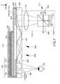
- Fig. 7 is a conceptual diagram of an image display device 300 in a display apparatus (head mounted display) of Embodiment 3.
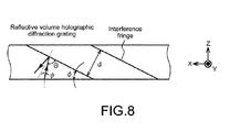
- Fig. 8 is a schematic cross-sectional diagram of a reflective volume holographic diffraction grating in a partially enlarged form.
- the image forming unit 111 is formed of the image forming unit having a first configuration, similarly in Embodiment 1.
- a light guide unit 320 is basically the same as the light guide unit 120 in Embodiment 1 in terms of structure and configuration except for differences in structures and configurations of the first deflection unit and the second deflection unit.
- parallel light that is diffracted and reflected in the first diffraction grating member 330 and is input to the light guide plate 321 at an angle of a direction approaching the second diffraction grating member 340 has a smaller angle formed together with the normal line of the light guide plate 321 when the light propagated inside the light guide plate 321 impinges on the internal surface of the light guide plate 321, than parallel light that is input to the light guide plate 321 at an angle of a direction opposite to the direction approaching the second diffraction grating member 340.
- the interference fringes formed in the second diffraction grating member 340 and the interference fringes formed in the first diffraction grating member 330 are symmetrical with respect to the virtual plane, which is vertical to the axis of the light guide plate 321.
- the surfaces of the first diffraction grating member 330 and the second diffraction grating member 340, which are not opposed to the light guide plate 321, are each covered with the protection member (protection plate) 326 so as to prevent the first diffraction grating member 330 and the second diffraction grating member 340 from being damaged.
- the light guide plate 321 and the protection member 326 are bonded to each other in their outer circumferential portions with the adhesive 327.
- the light guide plate 321 may be protected by attaching a transparent protection film to the first surface 322.
- the light guide plate 321 in Embodiment 4 that will be described later is basically the same as the light guide plate 321 described above in terms of structure and configuration.
- the first illumination sensor 801 in Embodiment 6 is applicable to the display apparatuses described in Embodiments 2 to 5.
- the first illumination sensor 801 may be formed of light-receiving elements provided to the imaging device for exposure measurement.
- Embodiment 7 is also a modification of Embodiments 1 to 4.
- Fig. 13A is a schematic diagram of a display apparatus of Embodiment 7 when viewed from above
- Fig. 13B is a schematic diagram of a circuit for controlling an illumination sensor.
- the comparison calculation circuit compares the calculation result of the illumination calculation circuit, i.e., illumination value, with a standard value.
- the transmitted-light illumination measurement sensor control circuit controls the dimming device 700 and/or the image forming unit 111 or 211 based on the value obtained by the comparison calculation circuit. Those circuits may be each formed of a well-known circuit. For controlling the dimming device 700, the light transmittance therein is controlled, and for controlling the image forming unit 111 or 211, the luminance of images to be formed thereby is controlled. It should be noted that the control over the light transmittance in the dimming device 700 and the control over the luminance of images formed by the image forming unit 111 or 211 may be executed separately or executed in correlation with each other.
- the second illumination sensor (transmitted-light illumination measurement sensor) 802 in Embodiment 7 is applicable to the display apparatuses described in Embodiments 2 to 4.
- the second illumination sensor 802 in Embodiment 7 may be combined with the first illumination sensor 801 in Embodiment 6 for use. If this is the case, with various tests, the control over the light transmittance in the dimming device 700 may be executed separately from or in correlation with the control over the luminance of images to be formed by the image forming unit 111 or 211.
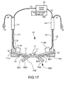
- FIG. 17 is a conceptual diagram of a modification of the display apparatus of Embodiment 8.
- An example shown in Fig. 15 is a modification of the display apparatuses of Embodiments 1 to 4, and an example shown in Fig. 17 is a modification of the display apparatus of Embodiment 5.
- the light shielding member 710 is provided to the light guide unit 120 on the side not provided with the image forming unit 111A or 111B, and is provided with a distance from the light guide unit 120.
- the light shielding member 710 is made of a non-transparent plastic material, for example.
- This light shielding member 710 is integrally extended from the casing 113 of the image display device 111A or 111B, or is attached to the casing 113 of the image forming unit 111A or 111 B.
- the light shielding member 710 is integrally extended from the frame 10, or is attached to the frame 10.
- the light shielding member 710 is integrally extended from the casing 113 of the image forming unit 111A or 111 B.
- Embodiment 11 is a modification of Embodiments 1 to 10.
- the light-transmission control material layer 705 is formed of a liquid crystal material layer.
- a light-transmission control material layer 705' is an optical shutter formed of an inorganic EL material layer.
- the inorganic EL material layer is made of tungstic oxide (WO 3 ).
- a first substrate 701' and a second substrate 703' are each a transparent glass substrate such as soda lime glass or super white glass, and the second substrate 703' is made thinner than the first substrate 701'.
- the second substrate 703' is formed with the thickness of 0.2 mm
- the first substrate 701' is formed with the thickness of 0.4 mm.
- the display apparatus of Embodiment 11 has the same structure and configuration as the display apparatuses of Embodiments 8 to 10, and thus detailed description thereof will be omitted.
- the first substrate 701' in the dimming device 700' is bonded to the protection member 126 using the adhesive 707 similarly to Embodiment 8.
- the image display device is typified by the image display device 100, but needless to say, the image display device 200, 300, 400, or 500 can be applied to the image display device.
- the illustration of the dimming device 700 is omitted.
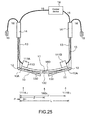
- the head mounted display of Embodiment 13 further includes a connection member 160 that connects the two image display devices 100.
- the connection member 160 is attached to one side of a frame 10, which faces the observer, at a central part 10C located between two pupils 21 of the observer 20 (i.e., attached between the observer 20 and the frame 10), with use of screws (not shown), for example.
- a projected image of the connection member 160 is included in a projected image of the frame 10. In other words, when the head mounted display is viewed from the front of the observer 20, the connection member 160 is hidden behind the frame 10, and the connection member 160 is not visually recognized.
- the mounting of the image forming units (specifically, image forming units 111A and 111 B) to both ends of the connection member 160 is specifically performed as follows, for example: three through-holes (not shown) are provided at three positions of each of the ends of the connection member; tapped hole portions (screw-engagement portions (not shown)) corresponding to the through-holes are provided to the image forming units 111A and 111B; and screws (not shown) are inserted into the respective through-holes and screwed into the hole portions provided to the image forming units 111A and 111 B.
- a spring is inserted in advance between each screw and a corresponding hole portion.
- connection members 160 and 170 are hatched.
- the connection member 160 is attached to the central part 10C of the frame 10 that is located between the two pupils 21 of the observer 20.
- the central part 10C corresponds to the bridge portion in normal eyeglasses.
- nose pads 10' are attached to the side of the connection member 160, which faces the observer 20. It should be noted that in Figs. 25 and 29 , the illustration of the nose pads 10' is omitted.
- the frame 10 and the connection member 160 are made of metal or plastic, and the shape of the connection member 160 is a curved bar-like shape.
- the connection member 160 connects the two image display devices 100, and the connection member 160 is attached to the central part 10C of the frame 10 that is located between the two pupils 21 of the observer 20.
- each of the image display devices 100 is not directly attached to the frame 10. So, when the frame 10 is mounted onto the head of the observer 20, the temple portions 13 are expanded outwards. As a result, even if the frame 10 is deformed, such a deformation of the frame 10 does not cause a displacement (positional change) of the image forming unit 111A or 111B, or causes little displacement, if any. For that reason, the angle of convergence of left and right images can be certainly prevented from being changed.
- Embodiment 14 is a modification of Embodiment 13.
- Fig. 27 is a schematic diagram of a head mounted display of Embodiment 14 when viewed from the front
- Fig. 28 is another schematic diagram of the head mounted display of Embodiment 14 (in a state assuming that a frame is removed) when viewed from the front
- Fig. 29 is a schematic diagram of the head mounted display of Embodiment 14 when viewed from above.
- a bar-like connection member 170 connects the two light guide units 120 instead of connecting the two image forming units 111A and 111 B. It should be noted that the two light guide units 120 may be integrally produced and the connection member 170 may be attached to such a light guide unit 120 integrally produced.
- connection member 170 is attached to the frame 10 at a central part 10C located between two pupils 21 of the observer 20 with use of screws, for example.
- the frame 10 and the image display devices have the same structures and configurations as the frame 10 and the image display devices described in Embodiment 13, and thus detailed description thereof will be omitted.
- the head mounted display of Embodiment 14 also has substantially the same structure and configuration as the head mounted display of Embodiment 13 except for the differences described above, and thus detailed description thereof will be omitted.
- the outer edge of the spatial area imaged by the imaging device 17A is displayed in the form of a frame 741 in the dimming device.
- light transmittance of the area 742 of the dimming device that corresponds to the spatial area imaged by the imaging device 17A may be made lower or higher than light transmittance of an area 743 of the dimming device that corresponds to the outside of the spatial area imaged by the imaging device 17A.
- the optical apparatus of Embodiment 15 may further include a dimming-device-controlling device, and the positions of the areas 741 and 742 of the dimming device that each correspond to the spatial area imaged by the imaging device may be corrected by the dimming-device-controlling device.
- the optical apparatus of Embodiment 15 includes a mobile phone or a smartphone, for example, or when the optical apparatus is combined with a mobile phone, a smartphone, or a personal computer, the spatial area imaged by the imaging device 17A may be displayed on the mobile phone, the smartphone, or the personal computer.
- the area 741 or 742 of the dimming device that corresponds to the spatial area imaged by the imaging device 17A is moved/turned or enlarged/contracted using the dimming-device-controlling device, which can be substituted by the mobile phone, the smartphone, or the personal computer.
- the difference between the spatial area displayed on the mobile phone, the smartphone, or the personal computer and the area 741 or 742 of the dimming device that corresponds to the spatial area imaged by the imaging device 17A may be eliminated.
- a surface relief hologram (see U.S. Patent Application No. 20040062505A1 ) may be disposed on a light guide plate.
- the diffraction grating element may be formed of the transmissive diffraction grating element.
- the first or second deflection unit may be formed of a reflective diffraction grating element, and the remaining one may be formed of a transmissive diffraction grating element.
- the diffraction grating element may be a reflective blazed diffraction grating element.
- an optical shutter may be used by application of electrodeposition/dissociation that occurs in response to the reversible oxidation reduction of metal, e.g., silver particles.
- metal e.g., silver particles.
- Ag + (silver) and I - (iodine) are dissolved in advance in an organic solvent, and Ag is precipitated by reduction of Ag + through appropriate voltage application to electrodes so that the dimming device is reduced in light transmittance.
- Ag is oxidized and dissolved as Ag + , so that the dimming device is increased in light transmittance.
- an optical shutter may be used by application of color change of substance that occurs in response to the oxidation reduction of an electrochromic material.
- the following configuration may also be exemplified other than the combination of a backlight that emits white light as a whole and a liquid crystal display including red, green, and blue light-emitting pixels.
- an image forming unit for color display including
- an image forming unit including: a light-emitting element 601 R that emits red light; a light passage control device (for example, liquid crystal display 604R) as a kind of light valve, configured to control the passage/non-passage of output light output from the light-emitting element 601 R that emits red light; a light-emitting element 601 G that emits green light; a light passage control device (for example, liquid crystal display 604G) as a kind of light valve, configured to control the passage/non-passage of output light output from the light-emitting element 601 G that emits green light; a light-emitting element 601 B that emits blue light; a light passage control device (for example, liquid crystal display 604B) as a kind of light valve, configured to control the passage/non-passage of output light output from the light-emitting element 601 B that emits green light; light leading members 602 configured to lead the light
- a display apparatus including:
- the display apparatus according to any one of [A01] to [A06], further including a sensor configured to measure brightness in an outside environment, in which the light transmittance of the partial area of the dimming device is further changed based on a measurement result of the brightness in the outside environment by the sensor.
- An optical apparatus comprising:
Landscapes
- Physics & Mathematics (AREA)
- General Physics & Mathematics (AREA)
- Optics & Photonics (AREA)
- Engineering & Computer Science (AREA)
- Computer Hardware Design (AREA)
- Theoretical Computer Science (AREA)
- Astronomy & Astrophysics (AREA)
- Instrument Panels (AREA)
- Devices For Indicating Variable Information By Combining Individual Elements (AREA)
- Spectroscopy & Molecular Physics (AREA)
Applications Claiming Priority (1)
| Application Number | Priority Date | Filing Date | Title |
|---|---|---|---|
| JP2014053191A JP6391952B2 (ja) | 2014-03-17 | 2014-03-17 | 表示装置及び光学装置 |
Publications (3)
| Publication Number | Publication Date |
|---|---|
| EP2930552A2 true EP2930552A2 (de) | 2015-10-14 |
| EP2930552A3 EP2930552A3 (de) | 2016-01-06 |
| EP2930552B1 EP2930552B1 (de) | 2023-06-14 |
Family
ID=52423606
Family Applications (1)
| Application Number | Title | Priority Date | Filing Date |
|---|---|---|---|
| EP15152708.2A Active EP2930552B1 (de) | 2014-03-17 | 2015-01-27 | Anzeigevorrichtung und optische Vorrichtung |
Country Status (4)
| Country | Link |
|---|---|
| US (1) | US10642040B2 (de) |
| EP (1) | EP2930552B1 (de) |
| JP (1) | JP6391952B2 (de) |
| CN (1) | CN104932102B (de) |
Cited By (1)
| Publication number | Priority date | Publication date | Assignee | Title |
|---|---|---|---|---|
| WO2020056384A1 (en) | 2018-09-14 | 2020-03-19 | Magic Leap, Inc. | Systems and methods for external light management |
Families Citing this family (50)
| Publication number | Priority date | Publication date | Assignee | Title |
|---|---|---|---|---|
| JP5434848B2 (ja) | 2010-08-18 | 2014-03-05 | ソニー株式会社 | 表示装置 |
| JP5780129B2 (ja) | 2011-11-22 | 2015-09-16 | ソニー株式会社 | 光ビーム伸長装置、画像表示装置及び光学装置 |
| JP5879973B2 (ja) | 2011-11-30 | 2016-03-08 | ソニー株式会社 | 光反射部材、光ビーム伸長装置、画像表示装置及び光学装置 |
| JP6003903B2 (ja) | 2012-01-24 | 2016-10-05 | ソニー株式会社 | 表示装置 |
| JP6145966B2 (ja) | 2012-05-09 | 2017-06-14 | ソニー株式会社 | 表示装置 |
| KR102097845B1 (ko) | 2013-01-10 | 2020-04-06 | 소니 주식회사 | 화상 표시 장치, 화상 생성 장치 및 투과형 공간 광변조 장치 |
| JP6123342B2 (ja) | 2013-02-20 | 2017-05-10 | ソニー株式会社 | 表示装置 |
| JP6547622B2 (ja) | 2013-04-11 | 2019-07-24 | ソニー株式会社 | 画像表示装置及び表示装置 |
| JP6358248B2 (ja) | 2013-04-11 | 2018-07-18 | ソニー株式会社 | 表示装置 |
| JP6367529B2 (ja) | 2013-06-25 | 2018-08-01 | ソニー株式会社 | 表示装置、表示制御方法、表示制御装置、および電子機器 |
| WO2015001839A1 (ja) | 2013-07-04 | 2015-01-08 | ソニー株式会社 | 表示装置 |
| EP3024221B1 (de) | 2013-07-16 | 2018-10-31 | Sony Corporation | Anzeigevorrichtung |
| CN104737060B (zh) | 2013-07-16 | 2018-12-11 | 索尼公司 | 显示装置 |
| JP2015148782A (ja) | 2014-02-10 | 2015-08-20 | ソニー株式会社 | 画像表示装置及び表示装置 |
| JP6314518B2 (ja) | 2014-02-10 | 2018-04-25 | ソニー株式会社 | 画像表示装置及び表示装置 |
| JP6201836B2 (ja) | 2014-03-14 | 2017-09-27 | ソニー株式会社 | 光学装置及びその組立方法、ホログラム回折格子、表示装置並びにアライメント装置 |
| JP2015184561A (ja) | 2014-03-25 | 2015-10-22 | ソニー株式会社 | 導光装置、画像表示装置及び表示装置 |
| JP2015184560A (ja) | 2014-03-25 | 2015-10-22 | ソニー株式会社 | 導光装置、画像表示装置及び表示装置 |
| US9568789B2 (en) * | 2014-11-19 | 2017-02-14 | Omnivision Technologies, Inc. | Panel carrier for a liquid crystal on silicon panel and method for electrically interconnecting same |
| US9633626B2 (en) * | 2015-03-12 | 2017-04-25 | Visteon Global Technologies, Inc. | Adjusting an electronic display based on gaze tracking |
| JP6844216B2 (ja) * | 2015-11-25 | 2021-03-17 | 株式会社リコー | 視認システム |
| FR3046850B1 (fr) | 2016-01-15 | 2018-01-26 | Universite De Strasbourg | Guide optique ameliore et systeme optique comportant un tel guide optique |
| CN107037610A (zh) * | 2016-02-04 | 2017-08-11 | 姜莹 | 隐形摄像眼镜 |
| EP4012480A1 (de) * | 2016-08-08 | 2022-06-15 | Essilor International | Am kopf montiertes gerät mit einem projektor zum projizieren eines bildes |
| TWI622803B (zh) * | 2016-08-30 | 2018-05-01 | 廣達電腦股份有限公司 | 頭戴式顯示裝置 |
| CN107919096A (zh) * | 2016-10-11 | 2018-04-17 | 中兴通讯股份有限公司 | 一种控制方法和头戴式设备 |
| US10534185B1 (en) | 2017-02-14 | 2020-01-14 | Facebook Technologies, Llc | Multi-planar display with waveguide and lens stacks |
| CN118311774A (zh) * | 2017-06-26 | 2024-07-09 | 京东方科技集团股份有限公司 | 显示系统和图像显示方法 |
| US10895746B1 (en) | 2017-08-07 | 2021-01-19 | Facebook Technologies, Llc | Expanding field-of-view in direct projection augmented reality and virtual reality systems |
| CN107422474B (zh) * | 2017-08-14 | 2020-12-01 | 京东方科技集团股份有限公司 | 一种光束扩展结构及光学显示模组 |
| JP6958106B2 (ja) * | 2017-08-21 | 2021-11-02 | セイコーエプソン株式会社 | 偏向装置、表示装置および偏向装置の製造方法 |
| US10534209B1 (en) * | 2017-08-21 | 2020-01-14 | Facebook Technologies, Llc | Liquid crystal structure for controlling brightness uniformity in a waveguide display |
| JP7156307B2 (ja) | 2017-11-21 | 2022-10-19 | Agc株式会社 | 光学ガラス、光学部材および光学機器 |
| CN107966819A (zh) * | 2017-12-27 | 2018-04-27 | 北京灵犀微光科技有限公司 | 波导显示装置 |
| US10942355B2 (en) * | 2018-01-22 | 2021-03-09 | Facebook Technologies, Llc | Systems, devices, and methods for tiled multi-monochromatic displays |
| US10613332B1 (en) | 2018-02-15 | 2020-04-07 | Facebook Technologies, Llc | Near-eye display assembly with enhanced display resolution |
| KR102084723B1 (ko) * | 2018-06-27 | 2020-03-04 | (주)비젼에이드 | 플라스틱 엘시디 셰이드를 구비한 증강현실 및 가상현실 겸용 스마트 글라스 디스플레이 장치 |
| WO2020023266A1 (en) * | 2018-07-23 | 2020-01-30 | Magic Leap, Inc. | Systems and methods for external light management |
| JP7155815B2 (ja) * | 2018-09-27 | 2022-10-19 | セイコーエプソン株式会社 | 頭部装着型表示装置 |
| WO2020115735A1 (en) * | 2018-12-05 | 2020-06-11 | Elbit Systems Ltd | Display illumination optics |
| FR3097658B1 (fr) * | 2019-06-20 | 2022-07-08 | Photonis France | Appareil de vision offrant une vision nocturne et une vision directe d'une scène environnante |
| CN110286538B (zh) * | 2019-06-28 | 2022-05-24 | Oppo广东移动通信有限公司 | 显示方法、显示装置、头戴式显示装置和存储介质 |
| CN110361866A (zh) * | 2019-07-11 | 2019-10-22 | Oppo广东移动通信有限公司 | 一种透射光强可调的头戴显示设备 |
| DE102019212989B3 (de) | 2019-08-29 | 2021-01-14 | Audi Ag | Kameravorrichtung zum Erzeugen von räumlich darstellenden Bilddaten einer Umgebung |
| CN110927969A (zh) | 2019-12-09 | 2020-03-27 | 京东方科技集团股份有限公司 | 光学显示系统和显示装置 |
| US12153220B2 (en) * | 2020-03-02 | 2024-11-26 | Carl Zeiss Meditec Ag | Head-mounted visualization system |
| CN111432132B (zh) * | 2020-05-09 | 2022-11-08 | 深圳传音控股股份有限公司 | 一种图像获取方法、装置及介质 |
| KR102876681B1 (ko) * | 2020-08-05 | 2025-10-27 | 삼성디스플레이 주식회사 | 표시 장치 |
| US20230041202A1 (en) * | 2021-08-03 | 2023-02-09 | Meta Platforms Technologies, Llc | Electronic circuit integration to smart glasses for enhanced reality applications |
| US11662525B1 (en) * | 2021-12-09 | 2023-05-30 | Visera Technologies Company Ltd. | Optical system |
Citations (3)
| Publication number | Priority date | Publication date | Assignee | Title |
|---|---|---|---|---|
| US20040062505A1 (en) | 2002-09-26 | 2004-04-01 | Mitsubishi Denki Kabushiki Kaisha | Optical active device |
| JP2005521099A (ja) | 2002-03-21 | 2005-07-14 | ラマス リミテッド | 光導体光学装置 |
| JP2006209144A (ja) | 2006-03-20 | 2006-08-10 | Sony Corp | 画像表示装置 |
Family Cites Families (101)
| Publication number | Priority date | Publication date | Assignee | Title |
|---|---|---|---|---|
| JPS5726822A (en) * | 1980-06-10 | 1982-02-13 | Seiko Epson Corp | Dimming spectacles |
| JPH01188826A (ja) | 1988-01-22 | 1989-07-28 | Fujitsu Ltd | 光シャッタ |
| JPH024212A (ja) | 1988-06-23 | 1990-01-09 | Stanley Electric Co Ltd | 液晶シャッタ素子 |
| US5224198A (en) | 1991-09-30 | 1993-06-29 | Motorola, Inc. | Waveguide virtual image display |
| JPH0888815A (ja) | 1994-09-19 | 1996-04-02 | Olympus Optical Co Ltd | 映像表示システム |
| JPH08160344A (ja) | 1994-12-05 | 1996-06-21 | Olympus Optical Co Ltd | 頭部装着式映像表示装置 |
| JP3630746B2 (ja) * | 1994-12-05 | 2005-03-23 | キヤノン株式会社 | 画像観察装置 |
| JPH10126711A (ja) | 1996-10-17 | 1998-05-15 | Olympus Optical Co Ltd | 頭部搭載型画像表示装置 |
| JPH10319240A (ja) | 1997-05-22 | 1998-12-04 | Fuji Xerox Co Ltd | ヘッドマウンテッドディスプレイ |
| WO1999056170A1 (en) | 1998-04-28 | 1999-11-04 | Citizen Watch Co., Ltd. | Reflection color liquid crystal display |
| JP2000171750A (ja) * | 1998-12-03 | 2000-06-23 | Sony Corp | ヘッドマウントディスプレイ、表示方法、および提供媒体 |
| JP5108966B2 (ja) | 2000-07-10 | 2012-12-26 | オリンパス株式会社 | 画像表示装置 |
| US6507286B2 (en) | 2000-12-29 | 2003-01-14 | Visteon Global Technologies, Inc. | Luminance control of automotive displays using an ambient light sensor |
| JP2003015075A (ja) | 2001-06-27 | 2003-01-15 | Nikon Corp | 電子眼鏡および眼鏡取付型表示装置 |
| JP2003280042A (ja) | 2002-03-26 | 2003-10-02 | Sharp Corp | 調光素子 |
| JP2004101197A (ja) | 2002-09-04 | 2004-04-02 | Sony Corp | 携帯型位置情報伝達装置及びナビゲーション方法 |
| US7049575B2 (en) | 2003-09-09 | 2006-05-23 | Apple Computer Inc. | System for sensing ambient light having ambient stability probability |
| IL157837A (en) * | 2003-09-10 | 2012-12-31 | Yaakov Amitai | Substrate-guided optical device particularly for three-dimensional displays |
| JP2005172851A (ja) | 2003-12-05 | 2005-06-30 | Sony Corp | 画像表示装置 |
| EP1731943B1 (de) | 2004-03-29 | 2019-02-13 | Sony Corporation | Optische einrichtung und virtuelle bildanzeigeeinrichtung |
| JP4572569B2 (ja) | 2004-04-19 | 2010-11-04 | 株式会社ニコン | 表示装置 |
| JP4742575B2 (ja) | 2004-12-03 | 2011-08-10 | 株式会社ニコン | 画像表示光学系及び画像表示装置 |
| EP1748305A4 (de) | 2004-05-17 | 2009-01-14 | Nikon Corp | Optisches element, optisches kombinierersystem und bildanzeigeeinheit |
| CN1957269A (zh) | 2004-05-17 | 2007-05-02 | 株式会社尼康 | 光学元件、合成器光学系统以及图像显示单元 |
| WO2006085310A1 (en) | 2005-02-10 | 2006-08-17 | Lumus Ltd. | Substrate-guided optical device particularly for vision enhanced optical systems |
| JP2006267887A (ja) | 2005-03-25 | 2006-10-05 | Konica Minolta Photo Imaging Inc | 映像認識手段を備えたヘッドマウントディスプレイ |
| JP5076282B2 (ja) | 2005-04-28 | 2012-11-21 | 三菱化学株式会社 | 表示装置 |
| KR101152141B1 (ko) | 2005-06-08 | 2012-06-15 | 삼성전자주식회사 | 액정표시패널과 액정표시패널의 제조방법 |
| US7965268B2 (en) * | 2005-07-08 | 2011-06-21 | Sharp Kabushiki Kaisha | Display device and liquid crystal display panel |
| CN102116962B (zh) | 2005-09-22 | 2012-09-05 | 夏普株式会社 | 液晶显示装置 |
| JP4810949B2 (ja) | 2005-09-29 | 2011-11-09 | ソニー株式会社 | 光学装置及び画像表示装置 |
| JP5226528B2 (ja) | 2005-11-21 | 2013-07-03 | マイクロビジョン,インク. | 像誘導基板を有するディスプレイ |
| JP4802806B2 (ja) * | 2006-03-28 | 2011-10-26 | ブラザー工業株式会社 | 画像表示装置 |
| JP2008009140A (ja) * | 2006-06-29 | 2008-01-17 | Fujitsu Ltd | 画像処理装置および画像処理方法 |
| JP2008067219A (ja) | 2006-09-08 | 2008-03-21 | Sony Corp | 撮像装置、撮像方法 |
| JP5017989B2 (ja) | 2006-09-27 | 2012-09-05 | ソニー株式会社 | 撮像装置、撮像方法 |
| JP2008103916A (ja) | 2006-10-18 | 2008-05-01 | Canon Inc | 頭部装着型画像表示装置およびシステム |
| US8225229B2 (en) | 2006-11-09 | 2012-07-17 | Sony Mobile Communications Ab | Adjusting display brightness and/or refresh rates based on eye tracking |
| WO2008078320A2 (en) * | 2006-12-22 | 2008-07-03 | Yossi Gross | Electronic transparency regulation element to enhance viewing through lens system |
| EP1990674A1 (de) | 2007-05-09 | 2008-11-12 | Harman Becker Automotive Systems GmbH | Am Kopf montierte Anzeigevorrichtung |
| US20090015740A1 (en) * | 2007-07-12 | 2009-01-15 | Ravil Sagitov | Window darkening system |
| RU2010105566A (ru) * | 2007-07-20 | 2011-12-10 | Раппапорт Фамили Инститют Фор Ресерч Ин Ве Медикал Саенсес (Il) | Способ и система для защиты сетчатой оболочки глаза от поражений, вызываемых светом |
| JP2009145513A (ja) | 2007-12-13 | 2009-07-02 | Konica Minolta Holdings Inc | 映像表示装置およびヘッドマウントディスプレイ |
| JP5169272B2 (ja) | 2008-02-12 | 2013-03-27 | ブラザー工業株式会社 | 画像表示装置 |
| JP2009251428A (ja) | 2008-04-09 | 2009-10-29 | Konica Minolta Holdings Inc | 情報表示システム |
| JP4681629B2 (ja) | 2008-05-21 | 2011-05-11 | 日本電信電話株式会社 | 表示デバイスのキャリブレーション方法及び装置 |
| US8514166B2 (en) * | 2008-05-29 | 2013-08-20 | Hong Kong Applied Science and Technology Research Institute Company Limited | LCD backlight dimming, LCD/image signal compensation and method of controlling an LCD display |
| WO2010062479A1 (en) | 2008-11-02 | 2010-06-03 | David Chaum | System and apparatus for eyeglass appliance platform |
| JP5321011B2 (ja) | 2008-11-25 | 2013-10-23 | ソニー株式会社 | 画像信号処理装置、画像信号処理方法および画像投射装置 |
| JP2010145674A (ja) | 2008-12-18 | 2010-07-01 | Konica Minolta Holdings Inc | 映像表示装置およびヘッドマウントディスプレイ |
| JP5136442B2 (ja) | 2009-01-27 | 2013-02-06 | ブラザー工業株式会社 | ヘッドマウントディスプレイ |
| JP5402293B2 (ja) | 2009-06-22 | 2014-01-29 | ソニー株式会社 | 頭部装着型ディスプレイ、及び、頭部装着型ディスプレイにおける画像表示方法 |
| JP2011053468A (ja) | 2009-09-02 | 2011-03-17 | Sony Corp | 映像/文字同時表示装置及び頭部装着型ディスプレイ |
| JP2011085769A (ja) | 2009-10-15 | 2011-04-28 | Canon Inc | 撮像表示装置 |
| US9091851B2 (en) * | 2010-02-28 | 2015-07-28 | Microsoft Technology Licensing, Llc | Light control in head mounted displays |
| US20120194420A1 (en) | 2010-02-28 | 2012-08-02 | Osterhout Group, Inc. | Ar glasses with event triggered user action control of ar eyepiece facility |
| US8477425B2 (en) * | 2010-02-28 | 2013-07-02 | Osterhout Group, Inc. | See-through near-eye display glasses including a partially reflective, partially transmitting optical element |
| JP5678460B2 (ja) | 2010-04-06 | 2015-03-04 | ソニー株式会社 | 頭部装着型ディスプレイ |
| JP5499854B2 (ja) | 2010-04-08 | 2014-05-21 | ソニー株式会社 | 頭部装着型ディスプレイにおける光学的位置調整方法 |
| JP5494153B2 (ja) | 2010-04-08 | 2014-05-14 | ソニー株式会社 | 頭部装着型ディスプレイにおける画像表示方法 |
| JP2012013940A (ja) | 2010-06-30 | 2012-01-19 | Sony Corp | 表示装置 |
| JP5434848B2 (ja) | 2010-08-18 | 2014-03-05 | ソニー株式会社 | 表示装置 |
| JP5732808B2 (ja) | 2010-10-19 | 2015-06-10 | セイコーエプソン株式会社 | 虚像表示装置 |
| JP5598281B2 (ja) | 2010-11-19 | 2014-10-01 | ソニー株式会社 | 投射型表示システム |
| JP5655626B2 (ja) | 2011-02-24 | 2015-01-21 | ソニー株式会社 | 画像処理装置、および画像処理方法、並びにプログラム |
| JP5732974B2 (ja) * | 2011-03-31 | 2015-06-10 | ソニー株式会社 | 光学装置および撮像装置 |
| US20120297014A1 (en) | 2011-05-18 | 2012-11-22 | Tomi Lahcanski | Method for compiling information from mobile communicators |
| JP2012252091A (ja) * | 2011-06-01 | 2012-12-20 | Sony Corp | 表示装置 |
| JP5790187B2 (ja) * | 2011-06-16 | 2015-10-07 | ソニー株式会社 | 表示装置 |
| CN103890809B (zh) * | 2011-08-30 | 2017-05-17 | 谷歌公司 | 显示所有物相关流 |
| US9323325B2 (en) | 2011-08-30 | 2016-04-26 | Microsoft Technology Licensing, Llc | Enhancing an object of interest in a see-through, mixed reality display device |
| US9087471B2 (en) | 2011-11-04 | 2015-07-21 | Google Inc. | Adaptive brightness control of head mounted display |
| JP5780129B2 (ja) | 2011-11-22 | 2015-09-16 | ソニー株式会社 | 光ビーム伸長装置、画像表示装置及び光学装置 |
| JP5879973B2 (ja) | 2011-11-30 | 2016-03-08 | ソニー株式会社 | 光反射部材、光ビーム伸長装置、画像表示装置及び光学装置 |
| JP6160020B2 (ja) | 2011-12-12 | 2017-07-12 | セイコーエプソン株式会社 | 透過型表示装置、表示方法および表示プログラム |
| JP6003903B2 (ja) * | 2012-01-24 | 2016-10-05 | ソニー株式会社 | 表示装置 |
| JP6035793B2 (ja) | 2012-03-14 | 2016-11-30 | ソニー株式会社 | 画像表示装置及び画像生成装置 |
| JP5884576B2 (ja) * | 2012-03-16 | 2016-03-15 | セイコーエプソン株式会社 | 頭部装着型表示装置および頭部装着型表示装置の制御方法 |
| US9096920B1 (en) | 2012-03-22 | 2015-08-04 | Google Inc. | User interface method |
| JP6060512B2 (ja) | 2012-04-02 | 2017-01-18 | セイコーエプソン株式会社 | 頭部装着型表示装置 |
| JP6145966B2 (ja) | 2012-05-09 | 2017-06-14 | ソニー株式会社 | 表示装置 |
| US9998687B2 (en) * | 2012-09-12 | 2018-06-12 | Bae Systems Information And Electronic Systems Integration Inc. | Face mounted extreme environment thermal sensor system |
| KR102097845B1 (ko) | 2013-01-10 | 2020-04-06 | 소니 주식회사 | 화상 표시 장치, 화상 생성 장치 및 투과형 공간 광변조 장치 |
| JP6123342B2 (ja) | 2013-02-20 | 2017-05-10 | ソニー株式会社 | 表示装置 |
| US20140253605A1 (en) * | 2013-03-05 | 2014-09-11 | John N. Border | Controlling brightness of a displayed image |
| JP6358248B2 (ja) | 2013-04-11 | 2018-07-18 | ソニー株式会社 | 表示装置 |
| JP6547622B2 (ja) | 2013-04-11 | 2019-07-24 | ソニー株式会社 | 画像表示装置及び表示装置 |
| JP2013210643A (ja) * | 2013-04-26 | 2013-10-10 | Sony Corp | 表示装置、表示方法 |
| JP2014225725A (ja) | 2013-05-15 | 2014-12-04 | ソニー株式会社 | 表示装置及び画像表示装置用光源 |
| JP6367529B2 (ja) | 2013-06-25 | 2018-08-01 | ソニー株式会社 | 表示装置、表示制御方法、表示制御装置、および電子機器 |
| WO2015001839A1 (ja) | 2013-07-04 | 2015-01-08 | ソニー株式会社 | 表示装置 |
| EP3024221B1 (de) | 2013-07-16 | 2018-10-31 | Sony Corporation | Anzeigevorrichtung |
| CN104737060B (zh) | 2013-07-16 | 2018-12-11 | 索尼公司 | 显示装置 |
| JP2015052635A (ja) | 2013-09-05 | 2015-03-19 | ソニー株式会社 | 光学ユニット、撮像装置 |
| KR20150081599A (ko) * | 2014-01-06 | 2015-07-15 | 삼성전자주식회사 | 디스플레이 장치 및 그 제어방법 |
| US9756257B2 (en) * | 2014-01-31 | 2017-09-05 | Hewlett-Packard Development Company, L.P. | Camera included in display |
| JP2015148782A (ja) | 2014-02-10 | 2015-08-20 | ソニー株式会社 | 画像表示装置及び表示装置 |
| JP6314518B2 (ja) | 2014-02-10 | 2018-04-25 | ソニー株式会社 | 画像表示装置及び表示装置 |
| JP6201836B2 (ja) | 2014-03-14 | 2017-09-27 | ソニー株式会社 | 光学装置及びその組立方法、ホログラム回折格子、表示装置並びにアライメント装置 |
| JP2015184561A (ja) | 2014-03-25 | 2015-10-22 | ソニー株式会社 | 導光装置、画像表示装置及び表示装置 |
| JP2015184560A (ja) | 2014-03-25 | 2015-10-22 | ソニー株式会社 | 導光装置、画像表示装置及び表示装置 |
-
2014
- 2014-03-17 JP JP2014053191A patent/JP6391952B2/ja active Active
-
2015
- 2015-01-27 EP EP15152708.2A patent/EP2930552B1/de active Active
- 2015-03-06 US US14/640,437 patent/US10642040B2/en active Active
- 2015-03-10 CN CN201510105367.4A patent/CN104932102B/zh active Active
Patent Citations (3)
| Publication number | Priority date | Publication date | Assignee | Title |
|---|---|---|---|---|
| JP2005521099A (ja) | 2002-03-21 | 2005-07-14 | ラマス リミテッド | 光導体光学装置 |
| US20040062505A1 (en) | 2002-09-26 | 2004-04-01 | Mitsubishi Denki Kabushiki Kaisha | Optical active device |
| JP2006209144A (ja) | 2006-03-20 | 2006-08-10 | Sony Corp | 画像表示装置 |
Cited By (7)
| Publication number | Priority date | Publication date | Assignee | Title |
|---|---|---|---|---|
| WO2020056384A1 (en) | 2018-09-14 | 2020-03-19 | Magic Leap, Inc. | Systems and methods for external light management |
| EP3850420A4 (de) * | 2018-09-14 | 2021-11-10 | Magic Leap, Inc. | Systeme und verfahren zur externen lichtverwaltung |
| US11428942B2 (en) | 2018-09-14 | 2022-08-30 | Magic Leap, Inc. | Systems and methods for external light management |
| US11719941B2 (en) | 2018-09-14 | 2023-08-08 | Magic Leap, Inc. | Systems and methods for external light management |
| US12032170B2 (en) | 2018-09-14 | 2024-07-09 | Magic Leap, Inc. | Systems and methods for external light management |
| US12379601B2 (en) | 2018-09-14 | 2025-08-05 | Magic Leap, Inc. | Systems and methods for external light management |
| EP4567499A3 (de) * | 2018-09-14 | 2025-08-13 | Magic Leap, Inc. | Systeme und verfahren zur externen lichtverwaltung |
Also Published As
| Publication number | Publication date |
|---|---|
| CN104932102B (zh) | 2020-06-12 |
| JP2015177405A (ja) | 2015-10-05 |
| EP2930552A3 (de) | 2016-01-06 |
| JP6391952B2 (ja) | 2018-09-19 |
| US10642040B2 (en) | 2020-05-05 |
| CN104932102A (zh) | 2015-09-23 |
| EP2930552B1 (de) | 2023-06-14 |
| US20150260995A1 (en) | 2015-09-17 |
Similar Documents
| Publication | Publication Date | Title |
|---|---|---|
| EP2930552B1 (de) | Anzeigevorrichtung und optische Vorrichtung | |
| US10540822B2 (en) | Display instrument and image display method | |
| US9933621B2 (en) | Light guide unit for an image display | |
| EP2924490B1 (de) | Lichtleitereinheit, Bildanzeigevorrichtung und Anzeigevorrichtung | |
| JP6988803B2 (ja) | 調光装置、画像表示装置及び表示装置 | |
| JP6872136B2 (ja) | 画像表示装置、表示装置、及び、表示装置の調整方法 | |
| CN110537136B (zh) | 光学装置、图像显示装置及显示装置 | |
| JP7207406B2 (ja) | 表示装置 | |
| US11520148B2 (en) | Optical device, image display device, and display apparatus | |
| US20220214550A1 (en) | Image display apparatus and display apparatus | |
| WO2017033601A1 (ja) | 表示装置、及び、表示装置の調整方法 |
Legal Events
| Date | Code | Title | Description |
|---|---|---|---|
| PUAI | Public reference made under article 153(3) epc to a published international application that has entered the european phase |
Free format text: ORIGINAL CODE: 0009012 |
|
| 17P | Request for examination filed |
Effective date: 20150226 |
|
| AK | Designated contracting states |
Kind code of ref document: A2 Designated state(s): AL AT BE BG CH CY CZ DE DK EE ES FI FR GB GR HR HU IE IS IT LI LT LU LV MC MK MT NL NO PL PT RO RS SE SI SK SM TR |
|
| AX | Request for extension of the european patent |
Extension state: BA ME |
|
| PUAL | Search report despatched |
Free format text: ORIGINAL CODE: 0009013 |
|
| AK | Designated contracting states |
Kind code of ref document: A3 Designated state(s): AL AT BE BG CH CY CZ DE DK EE ES FI FR GB GR HR HU IE IS IT LI LT LU LV MC MK MT NL NO PL PT RO RS SE SI SK SM TR |
|
| AX | Request for extension of the european patent |
Extension state: BA ME |
|
| RIC1 | Information provided on ipc code assigned before grant |
Ipc: G02C 7/10 20060101ALI20151202BHEP Ipc: G02B 27/01 20060101AFI20151202BHEP |
|
| STAA | Information on the status of an ep patent application or granted ep patent |
Free format text: STATUS: EXAMINATION IS IN PROGRESS |
|
| 17Q | First examination report despatched |
Effective date: 20180927 |
|
| RAP3 | Party data changed (applicant data changed or rights of an application transferred) |
Owner name: SONY GROUP CORPORATION |
|
| GRAP | Despatch of communication of intention to grant a patent |
Free format text: ORIGINAL CODE: EPIDOSNIGR1 |
|
| STAA | Information on the status of an ep patent application or granted ep patent |
Free format text: STATUS: GRANT OF PATENT IS INTENDED |
|
| RIC1 | Information provided on ipc code assigned before grant |
Ipc: G02B 27/14 20060101ALN20221213BHEP Ipc: G09G 5/10 20060101ALI20221213BHEP Ipc: G02B 23/14 20060101ALI20221213BHEP Ipc: G02B 27/01 20060101AFI20221213BHEP |
|
| INTG | Intention to grant announced |
Effective date: 20230116 |
|
| RIN1 | Information on inventor provided before grant (corrected) |
Inventor name: MUKAWA, HIROSHI |
|
| GRAS | Grant fee paid |
Free format text: ORIGINAL CODE: EPIDOSNIGR3 |
|
| GRAA | (expected) grant |
Free format text: ORIGINAL CODE: 0009210 |
|
| STAA | Information on the status of an ep patent application or granted ep patent |
Free format text: STATUS: THE PATENT HAS BEEN GRANTED |
|
| AK | Designated contracting states |
Kind code of ref document: B1 Designated state(s): AL AT BE BG CH CY CZ DE DK EE ES FI FR GB GR HR HU IE IS IT LI LT LU LV MC MK MT NL NO PL PT RO RS SE SI SK SM TR |
|
| REG | Reference to a national code |
Ref country code: CH Ref legal event code: EP |
|
| REG | Reference to a national code |
Ref country code: DE Ref legal event code: R096 Ref document number: 602015084165 Country of ref document: DE |
|
| REG | Reference to a national code |
Ref country code: AT Ref legal event code: REF Ref document number: 1579647 Country of ref document: AT Kind code of ref document: T Effective date: 20230715 |
|
| REG | Reference to a national code |
Ref country code: LT Ref legal event code: MG9D |
|
| REG | Reference to a national code |
Ref country code: NL Ref legal event code: MP Effective date: 20230614 |
|
| PG25 | Lapsed in a contracting state [announced via postgrant information from national office to epo] |
Ref country code: SE Free format text: LAPSE BECAUSE OF FAILURE TO SUBMIT A TRANSLATION OF THE DESCRIPTION OR TO PAY THE FEE WITHIN THE PRESCRIBED TIME-LIMIT Effective date: 20230614 Ref country code: NO Free format text: LAPSE BECAUSE OF FAILURE TO SUBMIT A TRANSLATION OF THE DESCRIPTION OR TO PAY THE FEE WITHIN THE PRESCRIBED TIME-LIMIT Effective date: 20230914 Ref country code: ES Free format text: LAPSE BECAUSE OF FAILURE TO SUBMIT A TRANSLATION OF THE DESCRIPTION OR TO PAY THE FEE WITHIN THE PRESCRIBED TIME-LIMIT Effective date: 20230614 |
|
| REG | Reference to a national code |
Ref country code: AT Ref legal event code: MK05 Ref document number: 1579647 Country of ref document: AT Kind code of ref document: T Effective date: 20230614 |
|
| PG25 | Lapsed in a contracting state [announced via postgrant information from national office to epo] |
Ref country code: RS Free format text: LAPSE BECAUSE OF FAILURE TO SUBMIT A TRANSLATION OF THE DESCRIPTION OR TO PAY THE FEE WITHIN THE PRESCRIBED TIME-LIMIT Effective date: 20230614 Ref country code: NL Free format text: LAPSE BECAUSE OF FAILURE TO SUBMIT A TRANSLATION OF THE DESCRIPTION OR TO PAY THE FEE WITHIN THE PRESCRIBED TIME-LIMIT Effective date: 20230614 Ref country code: LV Free format text: LAPSE BECAUSE OF FAILURE TO SUBMIT A TRANSLATION OF THE DESCRIPTION OR TO PAY THE FEE WITHIN THE PRESCRIBED TIME-LIMIT Effective date: 20230614 Ref country code: LT Free format text: LAPSE BECAUSE OF FAILURE TO SUBMIT A TRANSLATION OF THE DESCRIPTION OR TO PAY THE FEE WITHIN THE PRESCRIBED TIME-LIMIT Effective date: 20230614 Ref country code: HR Free format text: LAPSE BECAUSE OF FAILURE TO SUBMIT A TRANSLATION OF THE DESCRIPTION OR TO PAY THE FEE WITHIN THE PRESCRIBED TIME-LIMIT Effective date: 20230614 Ref country code: GR Free format text: LAPSE BECAUSE OF FAILURE TO SUBMIT A TRANSLATION OF THE DESCRIPTION OR TO PAY THE FEE WITHIN THE PRESCRIBED TIME-LIMIT Effective date: 20230915 |
|
| PG25 | Lapsed in a contracting state [announced via postgrant information from national office to epo] |
Ref country code: FI Free format text: LAPSE BECAUSE OF FAILURE TO SUBMIT A TRANSLATION OF THE DESCRIPTION OR TO PAY THE FEE WITHIN THE PRESCRIBED TIME-LIMIT Effective date: 20230614 |
|
| PG25 | Lapsed in a contracting state [announced via postgrant information from national office to epo] |
Ref country code: SK Free format text: LAPSE BECAUSE OF FAILURE TO SUBMIT A TRANSLATION OF THE DESCRIPTION OR TO PAY THE FEE WITHIN THE PRESCRIBED TIME-LIMIT Effective date: 20230614 |
|
| PGFP | Annual fee paid to national office [announced via postgrant information from national office to epo] |
Ref country code: GB Payment date: 20231219 Year of fee payment: 10 |
|
| PG25 | Lapsed in a contracting state [announced via postgrant information from national office to epo] |
Ref country code: IS Free format text: LAPSE BECAUSE OF FAILURE TO SUBMIT A TRANSLATION OF THE DESCRIPTION OR TO PAY THE FEE WITHIN THE PRESCRIBED TIME-LIMIT Effective date: 20231014 |
|
| PG25 | Lapsed in a contracting state [announced via postgrant information from national office to epo] |
Ref country code: SM Free format text: LAPSE BECAUSE OF FAILURE TO SUBMIT A TRANSLATION OF THE DESCRIPTION OR TO PAY THE FEE WITHIN THE PRESCRIBED TIME-LIMIT Effective date: 20230614 Ref country code: SK Free format text: LAPSE BECAUSE OF FAILURE TO SUBMIT A TRANSLATION OF THE DESCRIPTION OR TO PAY THE FEE WITHIN THE PRESCRIBED TIME-LIMIT Effective date: 20230614 Ref country code: RO Free format text: LAPSE BECAUSE OF FAILURE TO SUBMIT A TRANSLATION OF THE DESCRIPTION OR TO PAY THE FEE WITHIN THE PRESCRIBED TIME-LIMIT Effective date: 20230614 Ref country code: PT Free format text: LAPSE BECAUSE OF FAILURE TO SUBMIT A TRANSLATION OF THE DESCRIPTION OR TO PAY THE FEE WITHIN THE PRESCRIBED TIME-LIMIT Effective date: 20231016 Ref country code: IS Free format text: LAPSE BECAUSE OF FAILURE TO SUBMIT A TRANSLATION OF THE DESCRIPTION OR TO PAY THE FEE WITHIN THE PRESCRIBED TIME-LIMIT Effective date: 20231014 Ref country code: EE Free format text: LAPSE BECAUSE OF FAILURE TO SUBMIT A TRANSLATION OF THE DESCRIPTION OR TO PAY THE FEE WITHIN THE PRESCRIBED TIME-LIMIT Effective date: 20230614 Ref country code: CZ Free format text: LAPSE BECAUSE OF FAILURE TO SUBMIT A TRANSLATION OF THE DESCRIPTION OR TO PAY THE FEE WITHIN THE PRESCRIBED TIME-LIMIT Effective date: 20230614 Ref country code: AT Free format text: LAPSE BECAUSE OF FAILURE TO SUBMIT A TRANSLATION OF THE DESCRIPTION OR TO PAY THE FEE WITHIN THE PRESCRIBED TIME-LIMIT Effective date: 20230614 |
|
| PGFP | Annual fee paid to national office [announced via postgrant information from national office to epo] |
Ref country code: FR Payment date: 20231219 Year of fee payment: 10 |
|
| PG25 | Lapsed in a contracting state [announced via postgrant information from national office to epo] |
Ref country code: PL Free format text: LAPSE BECAUSE OF FAILURE TO SUBMIT A TRANSLATION OF THE DESCRIPTION OR TO PAY THE FEE WITHIN THE PRESCRIBED TIME-LIMIT Effective date: 20230614 |
|
| REG | Reference to a national code |
Ref country code: DE Ref legal event code: R097 Ref document number: 602015084165 Country of ref document: DE |
|
| PLBE | No opposition filed within time limit |
Free format text: ORIGINAL CODE: 0009261 |
|
| STAA | Information on the status of an ep patent application or granted ep patent |
Free format text: STATUS: NO OPPOSITION FILED WITHIN TIME LIMIT |
|
| PG25 | Lapsed in a contracting state [announced via postgrant information from national office to epo] |
Ref country code: DK Free format text: LAPSE BECAUSE OF FAILURE TO SUBMIT A TRANSLATION OF THE DESCRIPTION OR TO PAY THE FEE WITHIN THE PRESCRIBED TIME-LIMIT Effective date: 20230614 |
|
| PG25 | Lapsed in a contracting state [announced via postgrant information from national office to epo] |
Ref country code: SI Free format text: LAPSE BECAUSE OF FAILURE TO SUBMIT A TRANSLATION OF THE DESCRIPTION OR TO PAY THE FEE WITHIN THE PRESCRIBED TIME-LIMIT Effective date: 20230614 |
|
| P01 | Opt-out of the competence of the unified patent court (upc) registered |
Effective date: 20240329 |
|
| 26N | No opposition filed |
Effective date: 20240315 |
|
| PG25 | Lapsed in a contracting state [announced via postgrant information from national office to epo] |
Ref country code: SI Free format text: LAPSE BECAUSE OF FAILURE TO SUBMIT A TRANSLATION OF THE DESCRIPTION OR TO PAY THE FEE WITHIN THE PRESCRIBED TIME-LIMIT Effective date: 20230614 Ref country code: IT Free format text: LAPSE BECAUSE OF FAILURE TO SUBMIT A TRANSLATION OF THE DESCRIPTION OR TO PAY THE FEE WITHIN THE PRESCRIBED TIME-LIMIT Effective date: 20230614 |
|
| PG25 | Lapsed in a contracting state [announced via postgrant information from national office to epo] |
Ref country code: MC Free format text: LAPSE BECAUSE OF FAILURE TO SUBMIT A TRANSLATION OF THE DESCRIPTION OR TO PAY THE FEE WITHIN THE PRESCRIBED TIME-LIMIT Effective date: 20230614 |
|
| PG25 | Lapsed in a contracting state [announced via postgrant information from national office to epo] |
Ref country code: MC Free format text: LAPSE BECAUSE OF FAILURE TO SUBMIT A TRANSLATION OF THE DESCRIPTION OR TO PAY THE FEE WITHIN THE PRESCRIBED TIME-LIMIT Effective date: 20230614 |
|
| REG | Reference to a national code |
Ref country code: CH Ref legal event code: PL |
|
| PG25 | Lapsed in a contracting state [announced via postgrant information from national office to epo] |
Ref country code: LU Free format text: LAPSE BECAUSE OF NON-PAYMENT OF DUE FEES Effective date: 20240127 |
|
| PG25 | Lapsed in a contracting state [announced via postgrant information from national office to epo] |
Ref country code: LU Free format text: LAPSE BECAUSE OF NON-PAYMENT OF DUE FEES Effective date: 20240127 |
|
| PG25 | Lapsed in a contracting state [announced via postgrant information from national office to epo] |
Ref country code: BE Free format text: LAPSE BECAUSE OF NON-PAYMENT OF DUE FEES Effective date: 20240131 |
|
| PG25 | Lapsed in a contracting state [announced via postgrant information from national office to epo] |
Ref country code: CH Free format text: LAPSE BECAUSE OF NON-PAYMENT OF DUE FEES Effective date: 20240131 |
|
| PG25 | Lapsed in a contracting state [announced via postgrant information from national office to epo] |
Ref country code: CH Free format text: LAPSE BECAUSE OF NON-PAYMENT OF DUE FEES Effective date: 20240131 Ref country code: BE Free format text: LAPSE BECAUSE OF NON-PAYMENT OF DUE FEES Effective date: 20240131 |
|
| REG | Reference to a national code |
Ref country code: BE Ref legal event code: MM Effective date: 20240131 |
|
| PG25 | Lapsed in a contracting state [announced via postgrant information from national office to epo] |
Ref country code: BG Free format text: LAPSE BECAUSE OF FAILURE TO SUBMIT A TRANSLATION OF THE DESCRIPTION OR TO PAY THE FEE WITHIN THE PRESCRIBED TIME-LIMIT Effective date: 20230614 |
|
| PG25 | Lapsed in a contracting state [announced via postgrant information from national office to epo] |
Ref country code: BG Free format text: LAPSE BECAUSE OF FAILURE TO SUBMIT A TRANSLATION OF THE DESCRIPTION OR TO PAY THE FEE WITHIN THE PRESCRIBED TIME-LIMIT Effective date: 20230614 |
|
| PG25 | Lapsed in a contracting state [announced via postgrant information from national office to epo] |
Ref country code: IE Free format text: LAPSE BECAUSE OF NON-PAYMENT OF DUE FEES Effective date: 20240127 |
|
| PG25 | Lapsed in a contracting state [announced via postgrant information from national office to epo] |
Ref country code: IE Free format text: LAPSE BECAUSE OF NON-PAYMENT OF DUE FEES Effective date: 20240127 |
|
| PGFP | Annual fee paid to national office [announced via postgrant information from national office to epo] |
Ref country code: DE Payment date: 20241218 Year of fee payment: 11 |
|
| PG25 | Lapsed in a contracting state [announced via postgrant information from national office to epo] |
Ref country code: CY Free format text: LAPSE BECAUSE OF FAILURE TO SUBMIT A TRANSLATION OF THE DESCRIPTION OR TO PAY THE FEE WITHIN THE PRESCRIBED TIME-LIMIT; INVALID AB INITIO Effective date: 20150127 |
|
| PG25 | Lapsed in a contracting state [announced via postgrant information from national office to epo] |
Ref country code: HU Free format text: LAPSE BECAUSE OF FAILURE TO SUBMIT A TRANSLATION OF THE DESCRIPTION OR TO PAY THE FEE WITHIN THE PRESCRIBED TIME-LIMIT; INVALID AB INITIO Effective date: 20150127 |
|
| GBPC | Gb: european patent ceased through non-payment of renewal fee |
Effective date: 20250127 |
|
| PG25 | Lapsed in a contracting state [announced via postgrant information from national office to epo] |
Ref country code: GB Free format text: LAPSE BECAUSE OF NON-PAYMENT OF DUE FEES Effective date: 20250127 |
|
| PG25 | Lapsed in a contracting state [announced via postgrant information from national office to epo] |
Ref country code: FR Free format text: LAPSE BECAUSE OF NON-PAYMENT OF DUE FEES Effective date: 20250131 |
|
| PG25 | Lapsed in a contracting state [announced via postgrant information from national office to epo] |
Ref country code: TR Free format text: LAPSE BECAUSE OF FAILURE TO SUBMIT A TRANSLATION OF THE DESCRIPTION OR TO PAY THE FEE WITHIN THE PRESCRIBED TIME-LIMIT Effective date: 20230614 |