EP2915190B1 - Integrated bondline spacers for wafer level packaged circuit devices - Google Patents
Integrated bondline spacers for wafer level packaged circuit devices Download PDFInfo
- Publication number
- EP2915190B1 EP2915190B1 EP13850327.1A EP13850327A EP2915190B1 EP 2915190 B1 EP2915190 B1 EP 2915190B1 EP 13850327 A EP13850327 A EP 13850327A EP 2915190 B1 EP2915190 B1 EP 2915190B1
- Authority
- EP
- European Patent Office
- Prior art keywords
- layer
- wafer
- metal stack
- solder metal
- cap wafer
- Prior art date
- Legal status (The legal status is an assumption and is not a legal conclusion. Google has not performed a legal analysis and makes no representation as to the accuracy of the status listed.)
- Not-in-force
Links
Images


Classifications
-
- B—PERFORMING OPERATIONS; TRANSPORTING
- B81—MICROSTRUCTURAL TECHNOLOGY
- B81C—PROCESSES OR APPARATUS SPECIALLY ADAPTED FOR THE MANUFACTURE OR TREATMENT OF MICROSTRUCTURAL DEVICES OR SYSTEMS
- B81C1/00—Manufacture or treatment of devices or systems in or on a substrate
- B81C1/00015—Manufacture or treatment of devices or systems in or on a substrate for manufacturing microsystems
- B81C1/00261—Processes for packaging MEMS devices
- B81C1/00269—Bonding of solid lids or wafers to the substrate
-
- B—PERFORMING OPERATIONS; TRANSPORTING
- B81—MICROSTRUCTURAL TECHNOLOGY
- B81B—MICROSTRUCTURAL DEVICES OR SYSTEMS, e.g. MICROMECHANICAL DEVICES
- B81B7/00—Microstructural systems; Auxiliary parts of microstructural devices or systems
- B81B7/0032—Packages or encapsulation
- B81B7/0035—Packages or encapsulation for maintaining a controlled atmosphere inside of the chamber containing the MEMS
- B81B7/0041—Packages or encapsulation for maintaining a controlled atmosphere inside of the chamber containing the MEMS maintaining a controlled atmosphere with techniques not provided for in B81B7/0038
-
- B—PERFORMING OPERATIONS; TRANSPORTING
- B81—MICROSTRUCTURAL TECHNOLOGY
- B81B—MICROSTRUCTURAL DEVICES OR SYSTEMS, e.g. MICROMECHANICAL DEVICES
- B81B7/00—Microstructural systems; Auxiliary parts of microstructural devices or systems
- B81B7/0032—Packages or encapsulation
- B81B7/007—Interconnections between the MEMS and external electrical signals
-
- H—ELECTRICITY
- H01—ELECTRIC ELEMENTS
- H01L—SEMICONDUCTOR DEVICES NOT COVERED BY CLASS H10
- H01L23/00—Details of semiconductor or other solid state devices
- H01L23/02—Containers; Seals
- H01L23/04—Containers; Seals characterised by the shape of the container or parts, e.g. caps, walls
- H01L23/053—Containers; Seals characterised by the shape of the container or parts, e.g. caps, walls the container being a hollow construction and having an insulating or insulated base as a mounting for the semiconductor body
-
- B—PERFORMING OPERATIONS; TRANSPORTING
- B81—MICROSTRUCTURAL TECHNOLOGY
- B81C—PROCESSES OR APPARATUS SPECIALLY ADAPTED FOR THE MANUFACTURE OR TREATMENT OF MICROSTRUCTURAL DEVICES OR SYSTEMS
- B81C2203/00—Forming microstructural systems
- B81C2203/01—Packaging MEMS
- B81C2203/0172—Seals
- B81C2203/019—Seals characterised by the material or arrangement of seals between parts
-
- H—ELECTRICITY
- H01—ELECTRIC ELEMENTS
- H01L—SEMICONDUCTOR DEVICES NOT COVERED BY CLASS H10
- H01L2224/00—Indexing scheme for arrangements for connecting or disconnecting semiconductor or solid-state bodies and methods related thereto as covered by H01L24/00
- H01L2224/01—Means for bonding being attached to, or being formed on, the surface to be connected, e.g. chip-to-package, die-attach, "first-level" interconnects; Manufacturing methods related thereto
- H01L2224/26—Layer connectors, e.g. plate connectors, solder or adhesive layers; Manufacturing methods related thereto
- H01L2224/27—Manufacturing methods
- H01L2224/274—Manufacturing methods by blanket deposition of the material of the layer connector
- H01L2224/27444—Manufacturing methods by blanket deposition of the material of the layer connector in gaseous form
-
- H—ELECTRICITY
- H01—ELECTRIC ELEMENTS
- H01L—SEMICONDUCTOR DEVICES NOT COVERED BY CLASS H10
- H01L2224/00—Indexing scheme for arrangements for connecting or disconnecting semiconductor or solid-state bodies and methods related thereto as covered by H01L24/00
- H01L2224/01—Means for bonding being attached to, or being formed on, the surface to be connected, e.g. chip-to-package, die-attach, "first-level" interconnects; Manufacturing methods related thereto
- H01L2224/26—Layer connectors, e.g. plate connectors, solder or adhesive layers; Manufacturing methods related thereto
- H01L2224/27—Manufacturing methods
- H01L2224/274—Manufacturing methods by blanket deposition of the material of the layer connector
- H01L2224/2746—Plating
- H01L2224/27462—Electroplating
-
- H—ELECTRICITY
- H01—ELECTRIC ELEMENTS
- H01L—SEMICONDUCTOR DEVICES NOT COVERED BY CLASS H10
- H01L2224/00—Indexing scheme for arrangements for connecting or disconnecting semiconductor or solid-state bodies and methods related thereto as covered by H01L24/00
- H01L2224/01—Means for bonding being attached to, or being formed on, the surface to be connected, e.g. chip-to-package, die-attach, "first-level" interconnects; Manufacturing methods related thereto
- H01L2224/26—Layer connectors, e.g. plate connectors, solder or adhesive layers; Manufacturing methods related thereto
- H01L2224/27—Manufacturing methods
- H01L2224/274—Manufacturing methods by blanket deposition of the material of the layer connector
- H01L2224/2746—Plating
- H01L2224/27464—Electroless plating
-
- H—ELECTRICITY
- H01—ELECTRIC ELEMENTS
- H01L—SEMICONDUCTOR DEVICES NOT COVERED BY CLASS H10
- H01L2224/00—Indexing scheme for arrangements for connecting or disconnecting semiconductor or solid-state bodies and methods related thereto as covered by H01L24/00
- H01L2224/01—Means for bonding being attached to, or being formed on, the surface to be connected, e.g. chip-to-package, die-attach, "first-level" interconnects; Manufacturing methods related thereto
- H01L2224/26—Layer connectors, e.g. plate connectors, solder or adhesive layers; Manufacturing methods related thereto
- H01L2224/28—Structure, shape, material or disposition of the layer connectors prior to the connecting process
- H01L2224/29—Structure, shape, material or disposition of the layer connectors prior to the connecting process of an individual layer connector
- H01L2224/29001—Core members of the layer connector
- H01L2224/2901—Shape
- H01L2224/29011—Shape comprising apertures or cavities
-
- H—ELECTRICITY
- H01—ELECTRIC ELEMENTS
- H01L—SEMICONDUCTOR DEVICES NOT COVERED BY CLASS H10
- H01L2224/00—Indexing scheme for arrangements for connecting or disconnecting semiconductor or solid-state bodies and methods related thereto as covered by H01L24/00
- H01L2224/01—Means for bonding being attached to, or being formed on, the surface to be connected, e.g. chip-to-package, die-attach, "first-level" interconnects; Manufacturing methods related thereto
- H01L2224/26—Layer connectors, e.g. plate connectors, solder or adhesive layers; Manufacturing methods related thereto
- H01L2224/28—Structure, shape, material or disposition of the layer connectors prior to the connecting process
- H01L2224/29—Structure, shape, material or disposition of the layer connectors prior to the connecting process of an individual layer connector
- H01L2224/29001—Core members of the layer connector
- H01L2224/29099—Material
- H01L2224/291—Material with a principal constituent of the material being a metal or a metalloid, e.g. boron [B], silicon [Si], germanium [Ge], arsenic [As], antimony [Sb], tellurium [Te] and polonium [Po], and alloys thereof
-
- H—ELECTRICITY
- H01—ELECTRIC ELEMENTS
- H01L—SEMICONDUCTOR DEVICES NOT COVERED BY CLASS H10
- H01L2224/00—Indexing scheme for arrangements for connecting or disconnecting semiconductor or solid-state bodies and methods related thereto as covered by H01L24/00
- H01L2224/80—Methods for connecting semiconductor or other solid state bodies using means for bonding being attached to, or being formed on, the surface to be connected
- H01L2224/83—Methods for connecting semiconductor or other solid state bodies using means for bonding being attached to, or being formed on, the surface to be connected using a layer connector
- H01L2224/83001—Methods for connecting semiconductor or other solid state bodies using means for bonding being attached to, or being formed on, the surface to be connected using a layer connector involving a temporary auxiliary member not forming part of the bonding apparatus
-
- H—ELECTRICITY
- H01—ELECTRIC ELEMENTS
- H01L—SEMICONDUCTOR DEVICES NOT COVERED BY CLASS H10
- H01L2224/00—Indexing scheme for arrangements for connecting or disconnecting semiconductor or solid-state bodies and methods related thereto as covered by H01L24/00
- H01L2224/80—Methods for connecting semiconductor or other solid state bodies using means for bonding being attached to, or being formed on, the surface to be connected
- H01L2224/83—Methods for connecting semiconductor or other solid state bodies using means for bonding being attached to, or being formed on, the surface to be connected using a layer connector
- H01L2224/83007—Methods for connecting semiconductor or other solid state bodies using means for bonding being attached to, or being formed on, the surface to be connected using a layer connector involving a permanent auxiliary member being left in the finished device, e.g. aids for holding or protecting the layer connector during or after the bonding process
-
- H—ELECTRICITY
- H01—ELECTRIC ELEMENTS
- H01L—SEMICONDUCTOR DEVICES NOT COVERED BY CLASS H10
- H01L2224/00—Indexing scheme for arrangements for connecting or disconnecting semiconductor or solid-state bodies and methods related thereto as covered by H01L24/00
- H01L2224/80—Methods for connecting semiconductor or other solid state bodies using means for bonding being attached to, or being formed on, the surface to be connected
- H01L2224/83—Methods for connecting semiconductor or other solid state bodies using means for bonding being attached to, or being formed on, the surface to be connected using a layer connector
- H01L2224/8312—Aligning
- H01L2224/83136—Aligning involving guiding structures, e.g. spacers or supporting members
- H01L2224/83138—Aligning involving guiding structures, e.g. spacers or supporting members the guiding structures being at least partially left in the finished device
- H01L2224/83139—Guiding structures on the body
-
- H—ELECTRICITY
- H01—ELECTRIC ELEMENTS
- H01L—SEMICONDUCTOR DEVICES NOT COVERED BY CLASS H10
- H01L2224/00—Indexing scheme for arrangements for connecting or disconnecting semiconductor or solid-state bodies and methods related thereto as covered by H01L24/00
- H01L2224/80—Methods for connecting semiconductor or other solid state bodies using means for bonding being attached to, or being formed on, the surface to be connected
- H01L2224/83—Methods for connecting semiconductor or other solid state bodies using means for bonding being attached to, or being formed on, the surface to be connected using a layer connector
- H01L2224/8312—Aligning
- H01L2224/83136—Aligning involving guiding structures, e.g. spacers or supporting members
- H01L2224/83138—Aligning involving guiding structures, e.g. spacers or supporting members the guiding structures being at least partially left in the finished device
- H01L2224/8314—Guiding structures outside the body
-
- H—ELECTRICITY
- H01—ELECTRIC ELEMENTS
- H01L—SEMICONDUCTOR DEVICES NOT COVERED BY CLASS H10
- H01L2224/00—Indexing scheme for arrangements for connecting or disconnecting semiconductor or solid-state bodies and methods related thereto as covered by H01L24/00
- H01L2224/80—Methods for connecting semiconductor or other solid state bodies using means for bonding being attached to, or being formed on, the surface to be connected
- H01L2224/83—Methods for connecting semiconductor or other solid state bodies using means for bonding being attached to, or being formed on, the surface to be connected using a layer connector
- H01L2224/8312—Aligning
- H01L2224/83136—Aligning involving guiding structures, e.g. spacers or supporting members
- H01L2224/83138—Aligning involving guiding structures, e.g. spacers or supporting members the guiding structures being at least partially left in the finished device
- H01L2224/83141—Guiding structures both on and outside the body
-
- H—ELECTRICITY
- H01—ELECTRIC ELEMENTS
- H01L—SEMICONDUCTOR DEVICES NOT COVERED BY CLASS H10
- H01L2224/00—Indexing scheme for arrangements for connecting or disconnecting semiconductor or solid-state bodies and methods related thereto as covered by H01L24/00
- H01L2224/80—Methods for connecting semiconductor or other solid state bodies using means for bonding being attached to, or being formed on, the surface to be connected
- H01L2224/83—Methods for connecting semiconductor or other solid state bodies using means for bonding being attached to, or being formed on, the surface to be connected using a layer connector
- H01L2224/8319—Arrangement of the layer connectors prior to mounting
- H01L2224/83192—Arrangement of the layer connectors prior to mounting wherein the layer connectors are disposed only on another item or body to be connected to the semiconductor or solid-state body
-
- H—ELECTRICITY
- H01—ELECTRIC ELEMENTS
- H01L—SEMICONDUCTOR DEVICES NOT COVERED BY CLASS H10
- H01L2924/00—Indexing scheme for arrangements or methods for connecting or disconnecting semiconductor or solid-state bodies as covered by H01L24/00
- H01L2924/10—Details of semiconductor or other solid state devices to be connected
- H01L2924/146—Mixed devices
- H01L2924/1461—MEMS
-
- H—ELECTRICITY
- H01—ELECTRIC ELEMENTS
- H01L—SEMICONDUCTOR DEVICES NOT COVERED BY CLASS H10
- H01L2924/00—Indexing scheme for arrangements or methods for connecting or disconnecting semiconductor or solid-state bodies as covered by H01L24/00
- H01L2924/15—Details of package parts other than the semiconductor or other solid state devices to be connected
- H01L2924/161—Cap
- H01L2924/163—Connection portion, e.g. seal
Definitions
- the present disclosure relates generally to semiconductor device manufacturing and, more particularly, to bond gap control structures (BGCS) for wafer level packaged optical micro electromechanical systems (MEMS) devices.
- BGCS bond gap control structures
- MEMS micro electromechanical systems
- MEMS Microelectromechanical systems
- MEMS devices are integrated micro devices or systems combining electrical and mechanical components.
- MEMS devices may be fabricated using, for example, standard integrated circuit batch processing techniques.
- Exemplary applications for MEMS devices include sensing, controlling, and actuating on the micro scale.
- Such MEMS devices may function individually or in arrays to generate effects on a macro scale.
- MEMS devices require a vacuum environment in order to attain maximum performance.
- the vacuum package also provides protection and an optimal operating environment for the MEMS device.
- MEMS devices include infrared MEMS such as bolometers, and certain inertial MEMS such as gyros and accelerometers.
- MEMS devices have been individually packaged in vacuum compatible packages after fabrication and dicing of the MEMS device.
- the cost of packaging MEMS devices in traditional metal or ceramic packages may be on the order of about 10 to 100 times the device fabrication cost. This especially true if a vacuum is required in the package.
- These high packaging costs therefore make it difficult to develop commercially viable vacuum packaged MEMS devices.
- MEMS devices are fragile especially after dicing. Care must be taken in handling these devices, and traditional integrated circuit fabrication machinery cannot adequately handle and protect MEMS devices.
- special handling techniques have also been developed to protect the MEMS devices until vacuum packaging has been completed. These special handling procedures also add additional cost to the production of MEMS devices.
- Wafer Level Packaging was developed to address the high cost of packaging of MEMS by eliminating the traditional packages.
- two semiconductor wafers may be bonded together using a joining material to yield bonded wafers.
- a device wafer may be bonded to a lid wafer using an adhesive or solder to form a packaged MEMS device.
- Certain applications may require that the joining material form a substantially uniform bond line.
- substrates such as silicon wafers
- the joining material forms a bond line in between the substrates.
- the uniformity of the bond line may be affected by the flatness of the substrates and the uniformity of the bond force used to bond the wafers.
- the uniformity of the bond line may be controlled by placing spacers at certain intervals across the surface of one or both substrates. However, adding the spacers usually requires adding process steps to the fabrication process.
- US 2002/0000646 A1 discloses a method for vacuum packaging MEMS or similar devices during device fabrication comprising forming a plurality of MEMS devices, or similar devices, on a device wafer.
- US 2009/0029500 A1 discloses a method of manufacturing hermetic packaging for devices on a substrate wafer.
- a method of forming a wafer level packaged circuit device includes forming a device wafer, the device wafer including a first group of one or more material layers left remaining in a first region of a substrate of the device wafer; and forming a cap wafer configured to be attached to the device wafer, the cap wafer including a second group of one or more material layers left remaining in a second region of a substrate of the cap wafer; wherein a combined thickness of the first and second groups of one or more material layers defines an integrated bond gap control structure upon bonding of the device wafer and the cap wafer.
- a method of forming a wafer level packaged circuit device includes forming a device wafer, the device wafer including a polyimide layer formed in a first region of a substrate of the device wafer, and a first solder metal stack layer formed on the polyimide layer, wherein the polyimide layer is a same polyimide layer that is also used in the formation of micro electromechanical systems (MEMS) devices of an integrated circuit on the device wafer, and the first solder metal stack layer is also a same first solder metal stack layer used to form a sealing ring for the device wafer; forming a cap wafer, the cap wafer including an antireflective coating layer formed in a second region of a substrate of the cap wafer, and a second solder metal stack layer formed on the antireflective coating layer, wherein the antireflective coating layer is a same antireflective coating layer that is also formed on a cavity portion of the cap wafer, and the second solder metal stack layer is also a same second solder metal stack layer used
- a wafer level packaged circuit device in another embodiment, includes a device wafer bonded to a cap wafer.
- the device wafer includes a polyimide layer formed in a first region of a substrate of the device wafer, and a first solder metal stack layer formed on the polyimide layer, wherein the polyimide layer is a same polyimide layer that is also used in the formation of an integrated circuit on the device wafer, and the first solder metal stack layer is also a same first solder metal stack layer used to form a sealing ring for the device wafer.
- the cap wafer includes an antireflective coating layer formed in a second region of a substrate of the cap wafer, and a second solder metal stack layer formed on the antireflective coating layer, wherein the antireflective coating layer is a same antireflective coating layer that is also formed on a cavity portion of the cap wafer, and the second solder metal stack layer is also a same second solder metal stack layer used to form a sealing ring for the cap wafer; and an integrated bond gap control structure (BGCS) disposed between the device wafer and the cap wafer, the integrated BGCS comprising the polyimide layer, the first solder metal stack layer, the second solder metal stack layer, and the antireflective coating layer.
- BGCS integrated bond gap control structure
- a method of forming a wafer level packaged circuit device includes forming a device wafer; forming a cap wafer; forming, on either the cap wafer or the device wafer, a bond gap control structure comprising one or more material layers used in the formation of either the cap wafer or the device wafer, and left remaining in a region of a substrate of either the cap wafer or the device wafer; and bonding the cap wafer to the device wafer.
- infrared MEMS devices and certain other inertial MEMS devices require a vacuum environment to attain maximum performance.
- infrared microbolometers require an operating pressure of less than 10 millitorr (mT) to minimize thermal transfer from the detector elements to the substrate and package walls.
- vacuum compatible materials processes and equipment must be used.
- Infrared devices also require an optically transparent cover.
- a solution to high packaging costs is to eliminate the traditional individual vacuum packaging of a completed die. More specifically, this is achieved by moving the packaging step into the wafer fabrication area.
- a cap wafer is aligned and mounted to the device wafer with an annular seal ring of solder, or other sealing material, forming an enclosed cell at each die location.
- This cap attachment process is completed in a vacuum environment, leaving each MEMS device in a vacuum cell. Interconnects are brought out under the solder seal ring and are isolated by a dielectric layer.
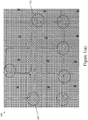
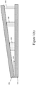
- Figure 1(a) illustrates an image of a bonded pair of wafers 100.
- the flatness of the substrates and the amount and uniformity of bond force largely determine the bond line geometries in terms of gap (thickness) and width.
- the bonded wafer pair 100 exhibits bond width and gap uniformity issues in the absence of a bond gap control structure or spacer (BGCS).
- BGCS bond gap control structure or spacer
- a BGCS may serve as a mechanical stop that controls the thickness of a bond line between two surfaces joined by solder, adhesive, or other joining material, and also prevents the joining material from spreading in an undesired manner.
- a BGCS may be disposable (i.e., may be removed during wafer dicing). If the BGCS is formed from materials that are not otherwise used in the formation of either the cap wafer or the device wafer (e.g., a polyimide or other material), then this results in additional processing steps. Any additional process or processes can in turn increase the risk of adding contamination in the form of particles or chemical residues to the optical window surfaces that are difficult to clean.
- the package fabrication process may easily be modified to leave small regions of these layers to form spacers of the materials that are already integral to the process.
- the present embodiments eliminate a separate spacer forming step in the cap wafer fabrication, which in turn involves spraying or spinning a separate layer of polyimide material (for example) on the wafer, photo-patterning the spacers, baking the material to harden it, and removing all residual traces from the optical surfaces.
- this approach also eliminates a possible need for capital equipment for the spray deposition of the polyimide, as it is often not compatible with photoresist dispensing equipment. Still another advantage is the simplification of the packaging process and enhancement of product yield by reducing risk of leaving residue on optical surfaces. Residue and particles are a prime caused of rejection for optical failures, and organic residue in the package is a prime cause of loss due to poor vacuum and shortened product life.
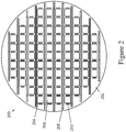
- the cap wafer 200 may, in one embodiment include a silicon substrate 202, although any suitable wafer substrate material may be used.
- the cap wafer 200 includes a plurality of cap sealing rings 204 corresponding in number to device sealing rings on an integrated circuit device wafer (not shown in Figure 2 ). Each of the cap sealing rings 204 corresponds to a device sealing ring so that the cap wafer 200 mates with a device wafer.
- Cavities 206 and bonding pad channels 208 are formed in the cap wafer 200 using an appropriate process such as wet or dry etching.
- the cavities 206 provide an increased volume for a vacuum packaged MEMS device (not shown in Figure 2 ), which in turn provides for a lower vacuum pressure level within the vacuum cell.
- the bonding pad channels 208 may be used to provide clearance over bonding pads (not shown in Figure 2 ) so that a dicing saw, etching process, or other suitable process may be used in a later step to open the lid wafer to expose the bonding pads for device testing before dicing of the wafer.
- the cap wafer 200 includes a plurality of bond gap control structures 210 adjacent the outer perimeter of the cap sealing rings 204.
- the bond gap control structures 210 serve as a mechanical stop that controls the thickness of a bond line between two joined surfaces.
- the bond gap control structures 210 are schematically depicted as single structures disposed in a y-axis direction with respect to Figure 2 , whereas the bonding pad channels 208 are generally disposed in an x-axis direction with respect to Figure 2 .
- other arrangements are also possible with respect to the cap wafer 200.
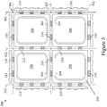
- Figure 3 is an enlarged top view of a patterned side of an exemplary cap wafer 300 that may also be used in accordance with the teachings herein.
- the substrate 202 has saw lines 302 depicted approximately in the center of scribe regions 304 where the substrate 202 is to be cut.
- a plurality of BGCSs 210 are disposed within the scribe regions 304, in both the x-axis and y-axis directions to operate as a mechanical stop that controls the geometry of a bond line of a cap sealing ring 204.
- the BGCS may only need to be disposed in either the x-axis or y-axis directions.
- the geometry of a bond line includes both gap thickness and width.
- the gap refers to the gap between bonded substrates, wherein the gap thickness is measured in a direction that is perpendicular to the flat surface of the substrate 202.
- the width is measured along the flat surface of substrate 202.
- a BGCS 210 may have any suitable size and shape.
- each BGCS 210 may have a width in any of the following ranges 1 to 10, 10 to 50, 50 to 100, or over 100 microns ( ⁇ m), a length in any of the following ranges 50 to 100, 100 to 200, or over 200 ⁇ m, and a thickness in any of the following ranges 1 to 5, 5 to 10, 10 to 20, or over 20.
- FIG. 4 there is shown a side cross sectional view of a portion of a device wafer 400 to be bonded to a corresponding portion of a cap wafer 200.
- the cap wafer 200 is shown in a bottom, cavity-up orientation and includes the substrate 202, etched out cavity 206, and a cap sealing ring 204a that surrounds the cavity 206. Adjacent sealing rings 204b are also shown for adjacent cavities on the cap wafer 202 for illustrative purposes.
- a cap wafer portion of each BGCS 210 is also illustrated on the cap wafer 200 in Figure 4 .
- a first layer for the BGCS 210 may include an antireflective (AR) coating layer 402 also formed on the thinned portions of the substrate 202 (i.e., corresponding to locations of the cavities 206 that will cover the corresponding MEMS devices on the device wafer 400), in accordance with the fabrication of infrared detectors or other such optical devices.
- the AR portion of the BGCS 210 may have a thickness on the order of about 5.5 ⁇ m to about 8.0 ⁇ m, and more specifically about 7.0 ⁇ m.
- the applicable patterning mask(s) are modified so that the AR material remains in the BGCS locations.
- a second layer for the BGCS 210 may include a solder base metal stack layer 404 that is also used as a solder base for the sealing rings 204a, 204b.
- the solder metal stack layer may include, for example, a layer of titanium (Ti), followed by a layer of nickel (Ni), and followed by a layer of gold (Au). Other metals, however, may also be used.
- the combined metal stack layer 404 may have an exemplary thickness on the order of about 0.4 ⁇ m to about 0.8 ⁇ m, and more specifically about 0.6 ⁇ m. The formation of the cap wafer is completed with the addition of an appropriate solder metal layer 406 atop the metal stack layer 404 of the sealing rings 204a, 204b.
- solder metal layer 406 is replaced by a material selected to obtain a vacuum tight seal.
- the solder metal layer 406 may be deposited through traditional integrated circuit fabrication techniques or other suitable deposition processes including, but not limited to, electroplating, electroless plating, and vacuum deposition.
- a substrate wafer 410 e.g., silicon
- the IC devices 412 may be MEMS devices such as a bolometer, for example, formed using traditional methods of integrated circuit fabrication.
- MEMS devices such as a bolometer
- the principles disclosed herein may be applied to vacuum packaging of any integrated circuit device, or similar device, formed on a substrate material and contained within a vacuum package.
- Each IC device 412 is configured to be aligned with a corresponding cavity 206 on the cap wafer 200.
- the device wafer 400 may be formed with one or more materials that match up with materials on the cap wafer 200 to formed integrated BGCSs.
- a device wafer portion of each BGCS is indicated at 414. That is, the device wafer portion 414 of a BGCS and the cap wafer portion 210 of a BGCS are mated to form an integrated BGCS, as shown hereinafter.
- a first layer for the device wafer portion 414 of a BGCS may include a sacrificial polyimide layer 416 that is used to thermally isolate the IC device 412 (e.g., bolometer) from the substrate 410.
- the polyimide layer 416 is not sacrificial in the BGCS regions, in that that layer patterning is adjusted such that the polyimide remains to contribute to the overall BGCS thickness.
- the polyimide layer 416 may have a thickness on the order of about 1.8 ⁇ m to about 2.0 ⁇ m.
- the device wafer 400 is provided with a solder base metal stack layer 418 that is used as a solder base to mate with the solder metal 406 atop the metal stack layer 404 of the sealing rings 204a, 204b.
- the solder metal stack layer 418 may also include a Ti/Ni/Au stack similar to stack 404, and at a substantially same thickness.
- the metal stack layer 418 may also serve as a second layer for the device wafer portion 414 of a BGCS. As particularly illustrated in Figure 4 , patterning of the metal stack layer 418 is such that it covers not only the top surface of the polyimide layer 416, but also the sidewall surfaces thereof.
- the arrangement is ready for final assembly.
- the cap wafer 200 may be placed in an assembly holder (not shown) with the solder layer 406 facing up.
- the device wafer 400 is aligned over the cap wafer 200 such that the metal stack layers 418 (i.e., not the metal stack layers 418 that are part of the integrated BGCS) are aligned over the corresponding cap wafer sealing rings 204a, 204b.
- Figure 5 depicts the joining of the cap wafer 200 with the device wafer 400 to form an assembly 500.
- an integrated BGCS indicated at the circled region 502 is defined by the combined material stack that includes the AR and solder metal layer 402, 404, respectively from the cap wafer 200 and the solder metal layer and polyimide layers 418, 416, respectively, from the device wafer 400.
- the integrated BGCSs like previous spacers, allow for good solder bond width and gap uniformity characteristics for the now-formed bond lines 504 in Figure 5 , but without the need to form the BGCSs using additional materials not otherwise used in forming either the cap wafer 200 or the device wafer 400.
- the bond lines may have an exemplary thickness on the order of about 10 ⁇ m as result of the combined thicknesses of the AR, polyimide and metal layers left in the scribe regions of the cap and device wafers.
- the assembly 500 is diced by sawing along, for example, a saw line 302 such as shown in Figure 3 , which may or may not result in the removal of the integrated BGCS shown at 502 in Figure 5 .
- the dicing of the assembly 500 may be accomplished by using traditional methods of dicing semiconductor wafers with completed integrated circuits.
- vacuum packaging MEMS devices 412 at the wafer level traditional methods of handling integrated circuit devices may be used since the vacuum package provides protection to the delicate MEMS device 412.
- a completed die representing a vacuum packaged MEMS device 412 may be mounted by chip-on-board methods or injection molded into a plastic package (not shown).
- a completed die may be placed in a non-vacuum package with other components (not shown).
- the integrated BGCSs 502 in Figure 5 is shown disposed in or proximate to a scribe region in between adjacent bond lines 504, it is also contemplated that the BGCSs 502 may also be positioned in additional locations.
- the BGCS materials from the cap wafer 200 and device wafer 400 could be patterned such that one or more BGCSs 502 reside within the confines of the sealed cavity, such as at location 506 for example. In this case, the BGCS 502 would remain as part of the completed product, after dicing.
- the cap wafer 200 includes a vacuum getter layer 602 initially formed on the inside surfaces of the cap substrate 202 over the AR layer, corresponding to the etched cavity regions 206.
- a getter is a deposit of reactive material that is placed inside a vacuum system, for the purpose of completing and maintaining the vacuum.
- the getter layer 602 may include one or more layers of elements such as titanium, zirconium, iron, and vanadium, to name a few examples.
- the getter layer 602 is left remaining atop the AR and solder base metal layers 402, 404, respectively, to become a part of the cap wafer portion of each BGCS 210.
- the assembly 700 includes integrated BGCSs, indicated by the dashed circled region 702.
- the getter layer 602 may have a thickness on the order of about 0.3 ⁇ m to about 2.0 ⁇ m, and more specifically about 0.9 ⁇ m.
- the embodiment of Figures 6 and 7 which uses the additional getter layer 602 in forming a BGCS, may provide for an additional bond line thickness of about 1.0 ⁇ m or more with respect to the embodiment of Figures 4 and 5 .
- reference number 802 depicts a width of a saw lane on the scribe region of the cap wafer substrate.
- the saw lane 802 may be on the order of about 480 ⁇ m.
- Region 804 represents the solder metal stack portion of the BGCS that covers the top and sidewall surfaces of the AR layer (not shown in Figure 8 ).
- Region 806 represents the getter layer portion of the BGCS that overlaps the top surface or plateau of the solder base metal, which is depicted by the dashed line 808.
- an exemplary width 810 of a shadowed edge overlap of the getter layer is on the order of about 40 ⁇ m.
- Figure 9 is a cross sectional, perspective view illustrating the placement of the vacuum getter layer 806 atop the solder metal layer stack 804 of Figure 8 .
- the AR layer depicted by region 902 is shown.
- the dashed lines 904 represent regions of a getter shadow mask, wherein a spacing 906 between the regions (i.e., the shadow mask opening width) represents the plateau width of the top of the solder metal stack 804 plus the shadowed edge width 810.
- the BGCSs are formed using existing materials for both the cap wafer 200 and the device wafer 400.
- the BGCS material could be formed from existing layers on either the cap wafer 200 alone or on the wafer layer 400 alone.
- the overall thickness of the BGCSs may be reduced and/or in the alternative, the existing layers used to form the cap wafer 200 or the device wafer 400 may be formed at a greater initial thickness so as to compensate for the BGCS material being formed on only one of the two wafers.
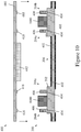
- Figure 10 is a side cross sectional view of a portion of a device wafer 400 to be bonded to a corresponding portion of a cap wafer 200 that results in the formation of integrated BGCSs, in accordance with another exemplary embodiment.
- the BCGS layer(s) are formed only on the cap wafer 200.
- the layer(s) are generally denoted at 1000, and may include one or more of the specific layers previously described as being formed on the cap wafer 200 such as, for example, AR layers, solder base metal stack layers, and getter layers.
- the BCGS layer(s) 1000 serve as the entire integrated BGCSs for the assembly 1100.
- the integrated BGCSs 1000 may be located elsewhere besides the scribe regions.
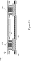
- Figure 12 is a side cross sectional view of a portion of a device wafer 400 to be bonded to a corresponding portion of a cap wafer 200 that results in the formation of integrated BGCSs, in accordance with another exemplary embodiment.
- the BCGS layer(s) are formed only on the device wafer 400.
- the BGCS layer(s) are generally denoted at 1200, and may include one or more of the specific layers previously described as being formed on the cap wafer 400 such as, for example, solder base metal stack layers and polyimide layers.
- the BCGS layer(s) 1200 serve as the entire integrated BGCSs for the assembly 1300.
- the BGCS material is advantageous taken from existing layers formed on the cap and/or device wafers that would ordinarily be removed from (or not initially formed in) the scribe regions of the wafers.
- exemplary materials include, but are not necessarily limited to, AR coatings, solder base metals, polyimides and vacuum getter layers.
Landscapes
- Engineering & Computer Science (AREA)
- Microelectronics & Electronic Packaging (AREA)
- Computer Hardware Design (AREA)
- Manufacturing & Machinery (AREA)
- Power Engineering (AREA)
- Physics & Mathematics (AREA)
- Condensed Matter Physics & Semiconductors (AREA)
- General Physics & Mathematics (AREA)
- Micromachines (AREA)
- Mechanical Treatment Of Semiconductor (AREA)
Priority Applications (1)
| Application Number | Priority Date | Filing Date | Title |
|---|---|---|---|
| EP18155856.0A EP3340294A1 (en) | 2012-11-02 | 2013-10-23 | Integrated bondline spacers for wafer level packaged circuit devices |
Applications Claiming Priority (2)
| Application Number | Priority Date | Filing Date | Title |
|---|---|---|---|
| US13/667,458 US8736045B1 (en) | 2012-11-02 | 2012-11-02 | Integrated bondline spacers for wafer level packaged circuit devices |
| PCT/US2013/066266 WO2014070534A2 (en) | 2012-11-02 | 2013-10-23 | Integrated bondline spacers for wafer level packaged circuit devices |
Related Child Applications (1)
| Application Number | Title | Priority Date | Filing Date |
|---|---|---|---|
| EP18155856.0A Division EP3340294A1 (en) | 2012-11-02 | 2013-10-23 | Integrated bondline spacers for wafer level packaged circuit devices |
Publications (3)
| Publication Number | Publication Date |
|---|---|
| EP2915190A2 EP2915190A2 (en) | 2015-09-09 |
| EP2915190A4 EP2915190A4 (en) | 2016-09-14 |
| EP2915190B1 true EP2915190B1 (en) | 2018-03-07 |
Family
ID=50621587
Family Applications (2)
| Application Number | Title | Priority Date | Filing Date |
|---|---|---|---|
| EP13850327.1A Not-in-force EP2915190B1 (en) | 2012-11-02 | 2013-10-23 | Integrated bondline spacers for wafer level packaged circuit devices |
| EP18155856.0A Withdrawn EP3340294A1 (en) | 2012-11-02 | 2013-10-23 | Integrated bondline spacers for wafer level packaged circuit devices |
Family Applications After (1)
| Application Number | Title | Priority Date | Filing Date |
|---|---|---|---|
| EP18155856.0A Withdrawn EP3340294A1 (en) | 2012-11-02 | 2013-10-23 | Integrated bondline spacers for wafer level packaged circuit devices |
Country Status (8)
| Country | Link |
|---|---|
| US (3) | US8736045B1 (enExample) |
| EP (2) | EP2915190B1 (enExample) |
| JP (1) | JP6412009B2 (enExample) |
| KR (1) | KR102164880B1 (enExample) |
| CA (1) | CA2889975C (enExample) |
| IL (2) | IL238325A0 (enExample) |
| NO (1) | NO2994775T3 (enExample) |
| WO (1) | WO2014070534A2 (enExample) |
Families Citing this family (22)
| Publication number | Priority date | Publication date | Assignee | Title |
|---|---|---|---|---|
| US8736045B1 (en) * | 2012-11-02 | 2014-05-27 | Raytheon Company | Integrated bondline spacers for wafer level packaged circuit devices |
| US9287188B2 (en) | 2013-02-05 | 2016-03-15 | Taiwan Semiconductor Manufacturing Company, Ltd. | Method and apparatus for a seal ring structure |
| US9673169B2 (en) | 2013-02-05 | 2017-06-06 | Taiwan Semiconductor Manufacturing Company, Ltd. | Method and apparatus for a wafer seal ring |
| US9540231B2 (en) * | 2014-01-28 | 2017-01-10 | Taiwan Semiconductor Manufacturing Co., Ltd. | MEMS device with a bonding layer embedded in the cap |
| CN104851848A (zh) * | 2014-02-17 | 2015-08-19 | 中芯国际集成电路制造(上海)有限公司 | 一种c-sam中接合晶圆的密封结构及其制备方法 |
| US9688529B2 (en) * | 2014-06-10 | 2017-06-27 | Qorvo Us, Inc. | Glass wafer assembly |
| US9334154B2 (en) | 2014-08-11 | 2016-05-10 | Raytheon Company | Hermetically sealed package having stress reducing layer |
| US9637372B2 (en) | 2015-04-27 | 2017-05-02 | Nxp Usa, Inc. | Bonded wafer structure having cavities with low pressure and method for forming |
| US9771258B2 (en) * | 2015-06-24 | 2017-09-26 | Raytheon Company | Wafer level MEMS package including dual seal ring |
| US20170081178A1 (en) * | 2015-09-22 | 2017-03-23 | Freescale Semiconductor, Inc. | Semiconductor device package with seal structure |
| US9570321B1 (en) * | 2015-10-20 | 2017-02-14 | Raytheon Company | Use of an external getter to reduce package pressure |
| DE102015224519A1 (de) * | 2015-12-08 | 2017-06-08 | Robert Bosch Gmbh | MEMS-Bauteil mit zwei unterschiedlichen Innendrücken |
| CN105731355B (zh) * | 2016-04-29 | 2017-05-31 | 合肥芯福传感器技术有限公司 | 一体化多功能陶瓷封装管壳 |
| JP6237969B1 (ja) * | 2017-03-29 | 2017-11-29 | 三菱電機株式会社 | 中空封止デバイス及びその製造方法 |
| CN107055456A (zh) * | 2017-04-14 | 2017-08-18 | 上海华虹宏力半导体制造有限公司 | 微机电系统器件的封装结构及方法 |
| CN107572474B (zh) * | 2017-08-22 | 2019-04-12 | 华中科技大学 | 一种封装间距可高精度控制的mems封装结构的封装方法 |
| CN109879240B (zh) * | 2017-12-06 | 2021-11-09 | 有研工程技术研究院有限公司 | 一种厚膜吸气材料的制备方法 |
| CN113603053B (zh) * | 2018-01-23 | 2024-01-23 | 苏州明皜传感科技股份有限公司 | 微机电系统装置 |
| US10830787B2 (en) * | 2018-02-20 | 2020-11-10 | General Electric Company | Optical accelerometers for use in navigation grade environments |
| EP4282811A4 (en) * | 2021-01-21 | 2024-11-20 | Hangzhou Hikmicro Sensing Technology Co., Ltd. | MEMS SENSOR AND ITS MANUFACTURING METHOD |
| CN113472314B (zh) * | 2021-07-22 | 2024-12-20 | 开元通信技术(厦门)有限公司 | 体声波滤波器及其制备方法 |
| DE102023210603A1 (de) * | 2023-10-26 | 2025-04-30 | Robert Bosch Gesellschaft mit beschränkter Haftung | Verfahren zum Verarbeiten eines Wafers |
Family Cites Families (18)
| Publication number | Priority date | Publication date | Assignee | Title |
|---|---|---|---|---|
| US5232962A (en) | 1991-10-09 | 1993-08-03 | Quantum Materials, Inc. | Adhesive bonding composition with bond line limiting spacer system |
| US6521477B1 (en) | 2000-02-02 | 2003-02-18 | Raytheon Company | Vacuum package fabrication of integrated circuit components |
| US20020179921A1 (en) * | 2001-06-02 | 2002-12-05 | Cohn Michael B. | Compliant hermetic package |
| US7952189B2 (en) * | 2004-05-27 | 2011-05-31 | Chang-Feng Wan | Hermetic packaging and method of manufacture and use therefore |
| US7576427B2 (en) | 2004-05-28 | 2009-08-18 | Stellar Micro Devices | Cold weld hermetic MEMS package and method of manufacture |
| US7442570B2 (en) * | 2005-03-18 | 2008-10-28 | Invensence Inc. | Method of fabrication of a AL/GE bonding in a wafer packaging environment and a product produced therefrom |
| US20070190747A1 (en) * | 2006-01-23 | 2007-08-16 | Tessera Technologies Hungary Kft. | Wafer level packaging to lidded chips |
| US20120132522A1 (en) | 2007-07-19 | 2012-05-31 | Innovative Micro Technology | Deposition/bonding chamber for encapsulated microdevices and method of use |
| US20090266480A1 (en) | 2008-04-29 | 2009-10-29 | International Business Machines Corporation | Process for Preparing a Solder Stand-Off |
| JP5610177B2 (ja) * | 2008-07-09 | 2014-10-22 | 国立大学法人東北大学 | 機能デバイス及びその製造方法 |
| DE102008042106A1 (de) * | 2008-09-15 | 2010-03-18 | Robert Bosch Gmbh | Verkapselung, MEMS sowie Verfahren zum Verkapseln |
| US8644125B2 (en) * | 2008-09-30 | 2014-02-04 | Intel Corporation | Seek scan probe (SSP) cantilever to mover wafer bond stop |
| JP5493767B2 (ja) * | 2009-11-25 | 2014-05-14 | 大日本印刷株式会社 | センサーユニットおよびその製造方法 |
| TWI511243B (zh) | 2009-12-31 | 2015-12-01 | 精材科技股份有限公司 | 晶片封裝體及其製造方法 |
| US8809784B2 (en) | 2010-10-21 | 2014-08-19 | Raytheon Company | Incident radiation detector packaging |
| US8454789B2 (en) * | 2010-11-05 | 2013-06-04 | Raytheon Company | Disposable bond gap control structures |
| US8507191B2 (en) * | 2011-01-07 | 2013-08-13 | Micron Technology, Inc. | Methods of forming a patterned, silicon-enriched developable antireflective material and semiconductor device structures including the same |
| US8736045B1 (en) | 2012-11-02 | 2014-05-27 | Raytheon Company | Integrated bondline spacers for wafer level packaged circuit devices |
-
2012
- 2012-11-02 US US13/667,458 patent/US8736045B1/en active Active
-
2013
- 2013-10-23 EP EP13850327.1A patent/EP2915190B1/en not_active Not-in-force
- 2013-10-23 EP EP18155856.0A patent/EP3340294A1/en not_active Withdrawn
- 2013-10-23 KR KR1020157014027A patent/KR102164880B1/ko not_active Expired - Fee Related
- 2013-10-23 JP JP2015541791A patent/JP6412009B2/ja not_active Expired - Fee Related
- 2013-10-23 CA CA2889975A patent/CA2889975C/en active Active
- 2013-10-23 WO PCT/US2013/066266 patent/WO2014070534A2/en not_active Ceased
-
2014
- 2014-03-10 US US14/202,756 patent/US9187312B2/en active Active
- 2014-05-07 NO NO14726898A patent/NO2994775T3/no unknown
- 2014-08-11 US US14/456,156 patent/US9174836B2/en active Active
-
2015
- 2015-04-16 IL IL238325A patent/IL238325A0/en active IP Right Grant
-
2018
- 2018-08-26 IL IL261373A patent/IL261373B/en active IP Right Grant
Non-Patent Citations (1)
| Title |
|---|
| None * |
Also Published As
| Publication number | Publication date |
|---|---|
| EP3340294A1 (en) | 2018-06-27 |
| NO2994775T3 (enExample) | 2018-02-03 |
| CA2889975A1 (en) | 2014-05-08 |
| JP6412009B2 (ja) | 2018-10-24 |
| IL261373A (en) | 2018-10-31 |
| JP2016504757A (ja) | 2016-02-12 |
| CA2889975C (en) | 2022-01-04 |
| EP2915190A2 (en) | 2015-09-09 |
| US20140124899A1 (en) | 2014-05-08 |
| US9187312B2 (en) | 2015-11-17 |
| US20140346643A1 (en) | 2014-11-27 |
| US9174836B2 (en) | 2015-11-03 |
| IL238325A0 (en) | 2015-06-30 |
| US20140193948A1 (en) | 2014-07-10 |
| WO2014070534A3 (en) | 2015-07-16 |
| KR102164880B1 (ko) | 2020-10-13 |
| EP2915190A4 (en) | 2016-09-14 |
| KR20150082363A (ko) | 2015-07-15 |
| US8736045B1 (en) | 2014-05-27 |
| IL261373B (en) | 2021-04-29 |
| WO2014070534A2 (en) | 2014-05-08 |
Similar Documents
| Publication | Publication Date | Title |
|---|---|---|
| EP2915190B1 (en) | Integrated bondline spacers for wafer level packaged circuit devices | |
| US6479320B1 (en) | Vacuum package fabrication of microelectromechanical system devices with integrated circuit components | |
| US6521477B1 (en) | Vacuum package fabrication of integrated circuit components | |
| US7682934B2 (en) | Wafer packaging and singulation method | |
| US7250353B2 (en) | Method and system of releasing a MEMS structure | |
| US8017435B2 (en) | Method for packaging electronic devices and integrated circuits | |
| WO2001056921A2 (en) | Vacuum package fabrication of microelectromechanical system devices with integrated circuit components | |
| US20100059835A1 (en) | Apparatus and Method of Wafer Bonding Using Compatible Alloy | |
| US7026189B2 (en) | Wafer packaging and singulation method | |
| CN101691200B (zh) | 非致冷红外探测器的低温真空封装结构及制作方法 | |
| US20170369309A1 (en) | Mems device formed by at least two bonded structural layers and manufacturing process thereof | |
| CN110015634B (zh) | 在前端中在晶片级沉积保护材料以进行早期颗粒和水分保护 | |
| CN111373303A (zh) | 异物除去方法及光检测装置的制造方法 | |
| KR100661350B1 (ko) | Mems 소자 패키지 및 그 제조방법 | |
| US9034679B2 (en) | Method for fabricating multiple types of MEMS devices | |
| US7510947B2 (en) | Method for wafer level packaging and fabricating cap structures | |
| TW202438435A (zh) | 製造半導體元件的方法和微鏡排列 | |
| US20120012963A1 (en) | Micro device packaging | |
| CN101016148B (zh) | 一种芯片级腔体密闭封装方法及封装结构 | |
| CN102020236B (zh) | 微机电系统芯片及其封装方法 | |
| NO20210884A1 (en) | Combined use of tin (Sn) thin film as the Solid-Liquid-InterDiffusion top layer metal layer for silicon chip and wafer stack bonding and as the masking film during silicon micromachining |
Legal Events
| Date | Code | Title | Description |
|---|---|---|---|
| PUAI | Public reference made under article 153(3) epc to a published international application that has entered the european phase |
Free format text: ORIGINAL CODE: 0009012 |
|
| 17P | Request for examination filed |
Effective date: 20150520 |
|
| AK | Designated contracting states |
Kind code of ref document: A2 Designated state(s): AL AT BE BG CH CY CZ DE DK EE ES FI FR GB GR HR HU IE IS IT LI LT LU LV MC MK MT NL NO PL PT RO RS SE SI SK SM TR |
|
| AX | Request for extension of the european patent |
Extension state: BA ME |
|
| DAX | Request for extension of the european patent (deleted) | ||
| A4 | Supplementary search report drawn up and despatched |
Effective date: 20160812 |
|
| RIC1 | Information provided on ipc code assigned before grant |
Ipc: H01L 23/544 20060101ALI20160808BHEP Ipc: H01L 23/48 20060101AFI20160808BHEP Ipc: H01L 21/56 20060101ALI20160808BHEP |
|
| 17Q | First examination report despatched |
Effective date: 20170314 |
|
| GRAP | Despatch of communication of intention to grant a patent |
Free format text: ORIGINAL CODE: EPIDOSNIGR1 |
|
| INTG | Intention to grant announced |
Effective date: 20170927 |
|
| GRAS | Grant fee paid |
Free format text: ORIGINAL CODE: EPIDOSNIGR3 |
|
| GRAA | (expected) grant |
Free format text: ORIGINAL CODE: 0009210 |
|
| AK | Designated contracting states |
Kind code of ref document: B1 Designated state(s): AL AT BE BG CH CY CZ DE DK EE ES FI FR GB GR HR HU IE IS IT LI LT LU LV MC MK MT NL NO PL PT RO RS SE SI SK SM TR |
|
| REG | Reference to a national code |
Ref country code: GB Ref legal event code: FG4D |
|
| REG | Reference to a national code |
Ref country code: CH Ref legal event code: EP Ref country code: AT Ref legal event code: REF Ref document number: 977408 Country of ref document: AT Kind code of ref document: T Effective date: 20180315 |
|
| REG | Reference to a national code |
Ref country code: DE Ref legal event code: R096 Ref document number: 602013034236 Country of ref document: DE |
|
| REG | Reference to a national code |
Ref country code: IE Ref legal event code: FG4D |
|
| REG | Reference to a national code |
Ref country code: NL Ref legal event code: MP Effective date: 20180307 |
|
| REG | Reference to a national code |
Ref country code: LT Ref legal event code: MG4D |
|
| PG25 | Lapsed in a contracting state [announced via postgrant information from national office to epo] |
Ref country code: FI Free format text: LAPSE BECAUSE OF FAILURE TO SUBMIT A TRANSLATION OF THE DESCRIPTION OR TO PAY THE FEE WITHIN THE PRESCRIBED TIME-LIMIT Effective date: 20180307 Ref country code: HR Free format text: LAPSE BECAUSE OF FAILURE TO SUBMIT A TRANSLATION OF THE DESCRIPTION OR TO PAY THE FEE WITHIN THE PRESCRIBED TIME-LIMIT Effective date: 20180307 Ref country code: CY Free format text: LAPSE BECAUSE OF FAILURE TO SUBMIT A TRANSLATION OF THE DESCRIPTION OR TO PAY THE FEE WITHIN THE PRESCRIBED TIME-LIMIT Effective date: 20180307 Ref country code: LT Free format text: LAPSE BECAUSE OF FAILURE TO SUBMIT A TRANSLATION OF THE DESCRIPTION OR TO PAY THE FEE WITHIN THE PRESCRIBED TIME-LIMIT Effective date: 20180307 Ref country code: ES Free format text: LAPSE BECAUSE OF FAILURE TO SUBMIT A TRANSLATION OF THE DESCRIPTION OR TO PAY THE FEE WITHIN THE PRESCRIBED TIME-LIMIT Effective date: 20180307 |
|
| REG | Reference to a national code |
Ref country code: NO Ref legal event code: T2 Effective date: 20180307 |
|
| REG | Reference to a national code |
Ref country code: AT Ref legal event code: MK05 Ref document number: 977408 Country of ref document: AT Kind code of ref document: T Effective date: 20180307 |
|
| PG25 | Lapsed in a contracting state [announced via postgrant information from national office to epo] |
Ref country code: BG Free format text: LAPSE BECAUSE OF FAILURE TO SUBMIT A TRANSLATION OF THE DESCRIPTION OR TO PAY THE FEE WITHIN THE PRESCRIBED TIME-LIMIT Effective date: 20180607 Ref country code: RS Free format text: LAPSE BECAUSE OF FAILURE TO SUBMIT A TRANSLATION OF THE DESCRIPTION OR TO PAY THE FEE WITHIN THE PRESCRIBED TIME-LIMIT Effective date: 20180307 Ref country code: GR Free format text: LAPSE BECAUSE OF FAILURE TO SUBMIT A TRANSLATION OF THE DESCRIPTION OR TO PAY THE FEE WITHIN THE PRESCRIBED TIME-LIMIT Effective date: 20180608 Ref country code: LV Free format text: LAPSE BECAUSE OF FAILURE TO SUBMIT A TRANSLATION OF THE DESCRIPTION OR TO PAY THE FEE WITHIN THE PRESCRIBED TIME-LIMIT Effective date: 20180307 Ref country code: SE Free format text: LAPSE BECAUSE OF FAILURE TO SUBMIT A TRANSLATION OF THE DESCRIPTION OR TO PAY THE FEE WITHIN THE PRESCRIBED TIME-LIMIT Effective date: 20180307 |
|
| REG | Reference to a national code |
Ref country code: FR Ref legal event code: PLFP Year of fee payment: 6 |
|
| PG25 | Lapsed in a contracting state [announced via postgrant information from national office to epo] |
Ref country code: RO Free format text: LAPSE BECAUSE OF FAILURE TO SUBMIT A TRANSLATION OF THE DESCRIPTION OR TO PAY THE FEE WITHIN THE PRESCRIBED TIME-LIMIT Effective date: 20180307 Ref country code: IT Free format text: LAPSE BECAUSE OF FAILURE TO SUBMIT A TRANSLATION OF THE DESCRIPTION OR TO PAY THE FEE WITHIN THE PRESCRIBED TIME-LIMIT Effective date: 20180307 Ref country code: EE Free format text: LAPSE BECAUSE OF FAILURE TO SUBMIT A TRANSLATION OF THE DESCRIPTION OR TO PAY THE FEE WITHIN THE PRESCRIBED TIME-LIMIT Effective date: 20180307 Ref country code: NL Free format text: LAPSE BECAUSE OF FAILURE TO SUBMIT A TRANSLATION OF THE DESCRIPTION OR TO PAY THE FEE WITHIN THE PRESCRIBED TIME-LIMIT Effective date: 20180307 Ref country code: PL Free format text: LAPSE BECAUSE OF FAILURE TO SUBMIT A TRANSLATION OF THE DESCRIPTION OR TO PAY THE FEE WITHIN THE PRESCRIBED TIME-LIMIT Effective date: 20180307 Ref country code: AL Free format text: LAPSE BECAUSE OF FAILURE TO SUBMIT A TRANSLATION OF THE DESCRIPTION OR TO PAY THE FEE WITHIN THE PRESCRIBED TIME-LIMIT Effective date: 20180307 |
|
| PG25 | Lapsed in a contracting state [announced via postgrant information from national office to epo] |
Ref country code: AT Free format text: LAPSE BECAUSE OF FAILURE TO SUBMIT A TRANSLATION OF THE DESCRIPTION OR TO PAY THE FEE WITHIN THE PRESCRIBED TIME-LIMIT Effective date: 20180307 Ref country code: SK Free format text: LAPSE BECAUSE OF FAILURE TO SUBMIT A TRANSLATION OF THE DESCRIPTION OR TO PAY THE FEE WITHIN THE PRESCRIBED TIME-LIMIT Effective date: 20180307 Ref country code: SM Free format text: LAPSE BECAUSE OF FAILURE TO SUBMIT A TRANSLATION OF THE DESCRIPTION OR TO PAY THE FEE WITHIN THE PRESCRIBED TIME-LIMIT Effective date: 20180307 Ref country code: CZ Free format text: LAPSE BECAUSE OF FAILURE TO SUBMIT A TRANSLATION OF THE DESCRIPTION OR TO PAY THE FEE WITHIN THE PRESCRIBED TIME-LIMIT Effective date: 20180307 |
|
| REG | Reference to a national code |
Ref country code: DE Ref legal event code: R097 Ref document number: 602013034236 Country of ref document: DE |
|
| PG25 | Lapsed in a contracting state [announced via postgrant information from national office to epo] |
Ref country code: PT Free format text: LAPSE BECAUSE OF FAILURE TO SUBMIT A TRANSLATION OF THE DESCRIPTION OR TO PAY THE FEE WITHIN THE PRESCRIBED TIME-LIMIT Effective date: 20180709 |
|
| PLBE | No opposition filed within time limit |
Free format text: ORIGINAL CODE: 0009261 |
|
| STAA | Information on the status of an ep patent application or granted ep patent |
Free format text: STATUS: NO OPPOSITION FILED WITHIN TIME LIMIT |
|
| PG25 | Lapsed in a contracting state [announced via postgrant information from national office to epo] |
Ref country code: DK Free format text: LAPSE BECAUSE OF FAILURE TO SUBMIT A TRANSLATION OF THE DESCRIPTION OR TO PAY THE FEE WITHIN THE PRESCRIBED TIME-LIMIT Effective date: 20180307 |
|
| 26N | No opposition filed |
Effective date: 20181210 |
|
| PG25 | Lapsed in a contracting state [announced via postgrant information from national office to epo] |
Ref country code: SI Free format text: LAPSE BECAUSE OF FAILURE TO SUBMIT A TRANSLATION OF THE DESCRIPTION OR TO PAY THE FEE WITHIN THE PRESCRIBED TIME-LIMIT Effective date: 20180307 |
|
| REG | Reference to a national code |
Ref country code: CH Ref legal event code: PL |
|
| REG | Reference to a national code |
Ref country code: BE Ref legal event code: MM Effective date: 20181031 |
|
| PG25 | Lapsed in a contracting state [announced via postgrant information from national office to epo] |
Ref country code: MC Free format text: LAPSE BECAUSE OF FAILURE TO SUBMIT A TRANSLATION OF THE DESCRIPTION OR TO PAY THE FEE WITHIN THE PRESCRIBED TIME-LIMIT Effective date: 20180307 Ref country code: LU Free format text: LAPSE BECAUSE OF NON-PAYMENT OF DUE FEES Effective date: 20181023 |
|
| REG | Reference to a national code |
Ref country code: IE Ref legal event code: MM4A |
|
| PG25 | Lapsed in a contracting state [announced via postgrant information from national office to epo] |
Ref country code: CH Free format text: LAPSE BECAUSE OF NON-PAYMENT OF DUE FEES Effective date: 20181031 Ref country code: BE Free format text: LAPSE BECAUSE OF NON-PAYMENT OF DUE FEES Effective date: 20181031 Ref country code: LI Free format text: LAPSE BECAUSE OF NON-PAYMENT OF DUE FEES Effective date: 20181031 |
|
| PG25 | Lapsed in a contracting state [announced via postgrant information from national office to epo] |
Ref country code: IE Free format text: LAPSE BECAUSE OF NON-PAYMENT OF DUE FEES Effective date: 20181023 |
|
| PG25 | Lapsed in a contracting state [announced via postgrant information from national office to epo] |
Ref country code: MT Free format text: LAPSE BECAUSE OF NON-PAYMENT OF DUE FEES Effective date: 20181023 |
|
| PG25 | Lapsed in a contracting state [announced via postgrant information from national office to epo] |
Ref country code: HU Free format text: LAPSE BECAUSE OF FAILURE TO SUBMIT A TRANSLATION OF THE DESCRIPTION OR TO PAY THE FEE WITHIN THE PRESCRIBED TIME-LIMIT; INVALID AB INITIO Effective date: 20131023 Ref country code: MK Free format text: LAPSE BECAUSE OF NON-PAYMENT OF DUE FEES Effective date: 20180307 |
|
| PG25 | Lapsed in a contracting state [announced via postgrant information from national office to epo] |
Ref country code: IS Free format text: LAPSE BECAUSE OF FAILURE TO SUBMIT A TRANSLATION OF THE DESCRIPTION OR TO PAY THE FEE WITHIN THE PRESCRIBED TIME-LIMIT Effective date: 20180707 |
|
| PGFP | Annual fee paid to national office [announced via postgrant information from national office to epo] |
Ref country code: TR Payment date: 20201020 Year of fee payment: 8 |
|
| PGFP | Annual fee paid to national office [announced via postgrant information from national office to epo] |
Ref country code: NO Payment date: 20201012 Year of fee payment: 8 |
|
| REG | Reference to a national code |
Ref country code: NO Ref legal event code: MMEP |
|
| PG25 | Lapsed in a contracting state [announced via postgrant information from national office to epo] |
Ref country code: NO Free format text: LAPSE BECAUSE OF NON-PAYMENT OF DUE FEES Effective date: 20211031 |
|
| P01 | Opt-out of the competence of the unified patent court (upc) registered |
Effective date: 20230530 |
|
| PGFP | Annual fee paid to national office [announced via postgrant information from national office to epo] |
Ref country code: GB Payment date: 20230920 Year of fee payment: 11 |
|
| PGFP | Annual fee paid to national office [announced via postgrant information from national office to epo] |
Ref country code: FR Payment date: 20230920 Year of fee payment: 11 |
|
| PGFP | Annual fee paid to national office [announced via postgrant information from national office to epo] |
Ref country code: DE Payment date: 20230920 Year of fee payment: 11 |
|
| PG25 | Lapsed in a contracting state [announced via postgrant information from national office to epo] |
Ref country code: TR Free format text: LAPSE BECAUSE OF NON-PAYMENT OF DUE FEES Effective date: 20211023 |
|
| REG | Reference to a national code |
Ref country code: DE Ref legal event code: R119 Ref document number: 602013034236 Country of ref document: DE |
|
| GBPC | Gb: european patent ceased through non-payment of renewal fee |
Effective date: 20241023 |
|
| PG25 | Lapsed in a contracting state [announced via postgrant information from national office to epo] |
Ref country code: DE Free format text: LAPSE BECAUSE OF NON-PAYMENT OF DUE FEES Effective date: 20250501 |
|
| PG25 | Lapsed in a contracting state [announced via postgrant information from national office to epo] |
Ref country code: GB Free format text: LAPSE BECAUSE OF NON-PAYMENT OF DUE FEES Effective date: 20241023 |
|
| PG25 | Lapsed in a contracting state [announced via postgrant information from national office to epo] |
Ref country code: FR Free format text: LAPSE BECAUSE OF NON-PAYMENT OF DUE FEES Effective date: 20241031 |