EP2913853A2 - Halbleiterbauelement - Google Patents
Halbleiterbauelement Download PDFInfo
- Publication number
- EP2913853A2 EP2913853A2 EP15150397.6A EP15150397A EP2913853A2 EP 2913853 A2 EP2913853 A2 EP 2913853A2 EP 15150397 A EP15150397 A EP 15150397A EP 2913853 A2 EP2913853 A2 EP 2913853A2
- Authority
- EP
- European Patent Office
- Prior art keywords
- nitride semiconductor
- semiconductor layer
- layer
- electrode
- semiconductor device
- Prior art date
- Legal status (The legal status is an assumption and is not a legal conclusion. Google has not performed a legal analysis and makes no representation as to the accuracy of the status listed.)
- Withdrawn
Links
- 239000004065 semiconductor Substances 0.000 title claims abstract description 216
- 230000008878 coupling Effects 0.000 claims abstract description 80
- 238000010168 coupling process Methods 0.000 claims abstract description 80
- 238000005859 coupling reaction Methods 0.000 claims abstract description 80
- 239000000758 substrate Substances 0.000 claims abstract description 63
- 230000000149 penetrating effect Effects 0.000 claims abstract description 24
- 150000004767 nitrides Chemical class 0.000 claims description 91
- 229910002704 AlGaN Inorganic materials 0.000 claims description 33
- 238000002955 isolation Methods 0.000 claims description 27
- 230000004888 barrier function Effects 0.000 abstract description 59
- 230000005533 two-dimensional electron gas Effects 0.000 abstract description 17
- 230000001965 increasing effect Effects 0.000 abstract description 7
- 239000010410 layer Substances 0.000 description 388
- 239000010408 film Substances 0.000 description 217
- 230000015572 biosynthetic process Effects 0.000 description 38
- 229910002601 GaN Inorganic materials 0.000 description 37
- JMASRVWKEDWRBT-UHFFFAOYSA-N Gallium nitride Chemical compound [Ga]#N JMASRVWKEDWRBT-UHFFFAOYSA-N 0.000 description 37
- 239000011229 interlayer Substances 0.000 description 29
- 238000004519 manufacturing process Methods 0.000 description 27
- 229920002120 photoresistant polymer Polymers 0.000 description 21
- NRTOMJZYCJJWKI-UHFFFAOYSA-N Titanium nitride Chemical compound [Ti]#N NRTOMJZYCJJWKI-UHFFFAOYSA-N 0.000 description 19
- 239000000463 material Substances 0.000 description 18
- 229910052751 metal Inorganic materials 0.000 description 12
- 239000002184 metal Substances 0.000 description 12
- 230000010287 polarization Effects 0.000 description 12
- 230000001681 protective effect Effects 0.000 description 12
- XUIMIQQOPSSXEZ-UHFFFAOYSA-N Silicon Chemical compound [Si] XUIMIQQOPSSXEZ-UHFFFAOYSA-N 0.000 description 10
- IJGRMHOSHXDMSA-UHFFFAOYSA-N nitrogen Substances N#N IJGRMHOSHXDMSA-UHFFFAOYSA-N 0.000 description 10
- 229910052710 silicon Inorganic materials 0.000 description 10
- 239000010703 silicon Substances 0.000 description 10
- 239000012535 impurity Substances 0.000 description 9
- 229910052782 aluminium Inorganic materials 0.000 description 8
- 230000005684 electric field Effects 0.000 description 8
- 230000006872 improvement Effects 0.000 description 8
- 229910052757 nitrogen Inorganic materials 0.000 description 7
- XAGFODPZIPBFFR-UHFFFAOYSA-N aluminium Chemical compound [Al] XAGFODPZIPBFFR-UHFFFAOYSA-N 0.000 description 6
- PIGFYZPCRLYGLF-UHFFFAOYSA-N Aluminum nitride Chemical compound [Al]#N PIGFYZPCRLYGLF-UHFFFAOYSA-N 0.000 description 5
- 230000000052 comparative effect Effects 0.000 description 5
- 230000007423 decrease Effects 0.000 description 5
- 238000005530 etching Methods 0.000 description 5
- -1 nitrogen ions Chemical class 0.000 description 5
- TWNQGVIAIRXVLR-UHFFFAOYSA-N oxo(oxoalumanyloxy)alumane Chemical compound O=[Al]O[Al]=O TWNQGVIAIRXVLR-UHFFFAOYSA-N 0.000 description 5
- 238000000206 photolithography Methods 0.000 description 5
- 239000011148 porous material Substances 0.000 description 5
- 238000004544 sputter deposition Methods 0.000 description 5
- 238000001947 vapour-phase growth Methods 0.000 description 5
- VYPSYNLAJGMNEJ-UHFFFAOYSA-N Silicium dioxide Chemical compound O=[Si]=O VYPSYNLAJGMNEJ-UHFFFAOYSA-N 0.000 description 4
- 238000010586 diagram Methods 0.000 description 4
- 229910052735 hafnium Inorganic materials 0.000 description 4
- 238000002513 implantation Methods 0.000 description 4
- 238000011835 investigation Methods 0.000 description 4
- 238000000623 plasma-assisted chemical vapour deposition Methods 0.000 description 4
- 229910052814 silicon oxide Inorganic materials 0.000 description 4
- 238000005229 chemical vapour deposition Methods 0.000 description 3
- PMHQVHHXPFUNSP-UHFFFAOYSA-M copper(1+);methylsulfanylmethane;bromide Chemical compound Br[Cu].CSC PMHQVHHXPFUNSP-UHFFFAOYSA-M 0.000 description 3
- 239000013078 crystal Substances 0.000 description 3
- 230000005669 field effect Effects 0.000 description 3
- 229910052733 gallium Inorganic materials 0.000 description 3
- VBJZVLUMGGDVMO-UHFFFAOYSA-N hafnium atom Chemical compound [Hf] VBJZVLUMGGDVMO-UHFFFAOYSA-N 0.000 description 3
- ZOXJGFHDIHLPTG-UHFFFAOYSA-N Boron Chemical compound [B] ZOXJGFHDIHLPTG-UHFFFAOYSA-N 0.000 description 2
- 229910052581 Si3N4 Inorganic materials 0.000 description 2
- 238000000231 atomic layer deposition Methods 0.000 description 2
- 229910052796 boron Inorganic materials 0.000 description 2
- 239000000470 constituent Substances 0.000 description 2
- 230000010354 integration Effects 0.000 description 2
- 150000002500 ions Chemical class 0.000 description 2
- 229910052594 sapphire Inorganic materials 0.000 description 2
- 239000010980 sapphire Substances 0.000 description 2
- HQVNEWCFYHHQES-UHFFFAOYSA-N silicon nitride Chemical compound N12[Si]34N5[Si]62N3[Si]51N64 HQVNEWCFYHHQES-UHFFFAOYSA-N 0.000 description 2
- 238000007740 vapor deposition Methods 0.000 description 2
- OKTJSMMVPCPJKN-UHFFFAOYSA-N Carbon Chemical compound [C] OKTJSMMVPCPJKN-UHFFFAOYSA-N 0.000 description 1
- GYHNNYVSQQEPJS-UHFFFAOYSA-N Gallium Chemical compound [Ga] GYHNNYVSQQEPJS-UHFFFAOYSA-N 0.000 description 1
- 229910003855 HfAlO Inorganic materials 0.000 description 1
- 229910004143 HfON Inorganic materials 0.000 description 1
- 229910004129 HfSiO Inorganic materials 0.000 description 1
- BPQQTUXANYXVAA-UHFFFAOYSA-N Orthosilicate Chemical compound [O-][Si]([O-])([O-])[O-] BPQQTUXANYXVAA-UHFFFAOYSA-N 0.000 description 1
- CEPICIBPGDWCRU-UHFFFAOYSA-N [Si].[Hf] Chemical compound [Si].[Hf] CEPICIBPGDWCRU-UHFFFAOYSA-N 0.000 description 1
- 229910052799 carbon Inorganic materials 0.000 description 1
- 230000015556 catabolic process Effects 0.000 description 1
- 230000000295 complement effect Effects 0.000 description 1
- 150000001875 compounds Chemical class 0.000 description 1
- 239000013039 cover film Substances 0.000 description 1
- 230000008030 elimination Effects 0.000 description 1
- 238000003379 elimination reaction Methods 0.000 description 1
- 229910000449 hafnium oxide Inorganic materials 0.000 description 1
- WIHZLLGSGQNAGK-UHFFFAOYSA-N hafnium(4+);oxygen(2-) Chemical compound [O-2].[O-2].[Hf+4] WIHZLLGSGQNAGK-UHFFFAOYSA-N 0.000 description 1
- CJNBYAVZURUTKZ-UHFFFAOYSA-N hafnium(IV) oxide Inorganic materials O=[Hf]=O CJNBYAVZURUTKZ-UHFFFAOYSA-N 0.000 description 1
- 238000010438 heat treatment Methods 0.000 description 1
- 239000012212 insulator Substances 0.000 description 1
- 238000005468 ion implantation Methods 0.000 description 1
- 230000004048 modification Effects 0.000 description 1
- 238000012986 modification Methods 0.000 description 1
- 238000002161 passivation Methods 0.000 description 1
- 230000009467 reduction Effects 0.000 description 1
- 230000001105 regulatory effect Effects 0.000 description 1
- 238000012827 research and development Methods 0.000 description 1
Images


Classifications
-
- H—ELECTRICITY
- H01—ELECTRIC ELEMENTS
- H01L—SEMICONDUCTOR DEVICES NOT COVERED BY CLASS H10
- H01L29/00—Semiconductor devices adapted for rectifying, amplifying, oscillating or switching, or capacitors or resistors with at least one potential-jump barrier or surface barrier, e.g. PN junction depletion layer or carrier concentration layer; Details of semiconductor bodies or of electrodes thereof ; Multistep manufacturing processes therefor
- H01L29/66—Types of semiconductor device ; Multistep manufacturing processes therefor
- H01L29/66007—Multistep manufacturing processes
- H01L29/66075—Multistep manufacturing processes of devices having semiconductor bodies comprising group 14 or group 13/15 materials
- H01L29/66227—Multistep manufacturing processes of devices having semiconductor bodies comprising group 14 or group 13/15 materials the devices being controllable only by the electric current supplied or the electric potential applied, to an electrode which does not carry the current to be rectified, amplified or switched, e.g. three-terminal devices
- H01L29/66409—Unipolar field-effect transistors
- H01L29/66477—Unipolar field-effect transistors with an insulated gate, i.e. MISFET
-
- H—ELECTRICITY
- H01—ELECTRIC ELEMENTS
- H01L—SEMICONDUCTOR DEVICES NOT COVERED BY CLASS H10
- H01L29/00—Semiconductor devices adapted for rectifying, amplifying, oscillating or switching, or capacitors or resistors with at least one potential-jump barrier or surface barrier, e.g. PN junction depletion layer or carrier concentration layer; Details of semiconductor bodies or of electrodes thereof ; Multistep manufacturing processes therefor
- H01L29/66—Types of semiconductor device ; Multistep manufacturing processes therefor
- H01L29/68—Types of semiconductor device ; Multistep manufacturing processes therefor controllable by only the electric current supplied, or only the electric potential applied, to an electrode which does not carry the current to be rectified, amplified or switched
- H01L29/76—Unipolar devices, e.g. field effect transistors
- H01L29/772—Field effect transistors
- H01L29/778—Field effect transistors with two-dimensional charge carrier gas channel, e.g. HEMT ; with two-dimensional charge-carrier layer formed at a heterojunction interface
- H01L29/7786—Field effect transistors with two-dimensional charge carrier gas channel, e.g. HEMT ; with two-dimensional charge-carrier layer formed at a heterojunction interface with direct single heterostructure, i.e. with wide bandgap layer formed on top of active layer, e.g. direct single heterostructure MIS-like HEMT
- H01L29/7787—Field effect transistors with two-dimensional charge carrier gas channel, e.g. HEMT ; with two-dimensional charge-carrier layer formed at a heterojunction interface with direct single heterostructure, i.e. with wide bandgap layer formed on top of active layer, e.g. direct single heterostructure MIS-like HEMT with wide bandgap charge-carrier supplying layer, e.g. direct single heterostructure MODFET
-
- H—ELECTRICITY
- H01—ELECTRIC ELEMENTS
- H01L—SEMICONDUCTOR DEVICES NOT COVERED BY CLASS H10
- H01L29/00—Semiconductor devices adapted for rectifying, amplifying, oscillating or switching, or capacitors or resistors with at least one potential-jump barrier or surface barrier, e.g. PN junction depletion layer or carrier concentration layer; Details of semiconductor bodies or of electrodes thereof ; Multistep manufacturing processes therefor
- H01L29/02—Semiconductor bodies ; Multistep manufacturing processes therefor
- H01L29/06—Semiconductor bodies ; Multistep manufacturing processes therefor characterised by their shape; characterised by the shapes, relative sizes, or dispositions of the semiconductor regions ; characterised by the concentration or distribution of impurities within semiconductor regions
- H01L29/10—Semiconductor bodies ; Multistep manufacturing processes therefor characterised by their shape; characterised by the shapes, relative sizes, or dispositions of the semiconductor regions ; characterised by the concentration or distribution of impurities within semiconductor regions with semiconductor regions connected to an electrode not carrying current to be rectified, amplified or switched and such electrode being part of a semiconductor device which comprises three or more electrodes
- H01L29/107—Substrate region of field-effect devices
- H01L29/1075—Substrate region of field-effect devices of field-effect transistors
- H01L29/1079—Substrate region of field-effect devices of field-effect transistors with insulated gate
- H01L29/1087—Substrate region of field-effect devices of field-effect transistors with insulated gate characterised by the contact structure of the substrate region, e.g. for controlling or preventing bipolar effect
-
- H—ELECTRICITY
- H01—ELECTRIC ELEMENTS
- H01L—SEMICONDUCTOR DEVICES NOT COVERED BY CLASS H10
- H01L29/00—Semiconductor devices adapted for rectifying, amplifying, oscillating or switching, or capacitors or resistors with at least one potential-jump barrier or surface barrier, e.g. PN junction depletion layer or carrier concentration layer; Details of semiconductor bodies or of electrodes thereof ; Multistep manufacturing processes therefor
- H01L29/02—Semiconductor bodies ; Multistep manufacturing processes therefor
- H01L29/12—Semiconductor bodies ; Multistep manufacturing processes therefor characterised by the materials of which they are formed
- H01L29/20—Semiconductor bodies ; Multistep manufacturing processes therefor characterised by the materials of which they are formed including, apart from doping materials or other impurities, only AIIIBV compounds
- H01L29/2003—Nitride compounds
-
- H—ELECTRICITY
- H01—ELECTRIC ELEMENTS
- H01L—SEMICONDUCTOR DEVICES NOT COVERED BY CLASS H10
- H01L29/00—Semiconductor devices adapted for rectifying, amplifying, oscillating or switching, or capacitors or resistors with at least one potential-jump barrier or surface barrier, e.g. PN junction depletion layer or carrier concentration layer; Details of semiconductor bodies or of electrodes thereof ; Multistep manufacturing processes therefor
- H01L29/02—Semiconductor bodies ; Multistep manufacturing processes therefor
- H01L29/12—Semiconductor bodies ; Multistep manufacturing processes therefor characterised by the materials of which they are formed
- H01L29/20—Semiconductor bodies ; Multistep manufacturing processes therefor characterised by the materials of which they are formed including, apart from doping materials or other impurities, only AIIIBV compounds
- H01L29/201—Semiconductor bodies ; Multistep manufacturing processes therefor characterised by the materials of which they are formed including, apart from doping materials or other impurities, only AIIIBV compounds including two or more compounds, e.g. alloys
- H01L29/205—Semiconductor bodies ; Multistep manufacturing processes therefor characterised by the materials of which they are formed including, apart from doping materials or other impurities, only AIIIBV compounds including two or more compounds, e.g. alloys in different semiconductor regions, e.g. heterojunctions
-
- H—ELECTRICITY
- H01—ELECTRIC ELEMENTS
- H01L—SEMICONDUCTOR DEVICES NOT COVERED BY CLASS H10
- H01L29/00—Semiconductor devices adapted for rectifying, amplifying, oscillating or switching, or capacitors or resistors with at least one potential-jump barrier or surface barrier, e.g. PN junction depletion layer or carrier concentration layer; Details of semiconductor bodies or of electrodes thereof ; Multistep manufacturing processes therefor
- H01L29/40—Electrodes ; Multistep manufacturing processes therefor
- H01L29/41—Electrodes ; Multistep manufacturing processes therefor characterised by their shape, relative sizes or dispositions
- H01L29/417—Electrodes ; Multistep manufacturing processes therefor characterised by their shape, relative sizes or dispositions carrying the current to be rectified, amplified or switched
- H01L29/41725—Source or drain electrodes for field effect devices
- H01L29/4175—Source or drain electrodes for field effect devices for lateral devices where the connection to the source or drain region is done through at least one part of the semiconductor substrate thickness, e.g. with connecting sink or with via-hole
-
- H—ELECTRICITY
- H01—ELECTRIC ELEMENTS
- H01L—SEMICONDUCTOR DEVICES NOT COVERED BY CLASS H10
- H01L29/00—Semiconductor devices adapted for rectifying, amplifying, oscillating or switching, or capacitors or resistors with at least one potential-jump barrier or surface barrier, e.g. PN junction depletion layer or carrier concentration layer; Details of semiconductor bodies or of electrodes thereof ; Multistep manufacturing processes therefor
- H01L29/40—Electrodes ; Multistep manufacturing processes therefor
- H01L29/41—Electrodes ; Multistep manufacturing processes therefor characterised by their shape, relative sizes or dispositions
- H01L29/423—Electrodes ; Multistep manufacturing processes therefor characterised by their shape, relative sizes or dispositions not carrying the current to be rectified, amplified or switched
- H01L29/42312—Gate electrodes for field effect devices
- H01L29/42316—Gate electrodes for field effect devices for field-effect transistors
- H01L29/4232—Gate electrodes for field effect devices for field-effect transistors with insulated gate
- H01L29/42356—Disposition, e.g. buried gate electrode
- H01L29/4236—Disposition, e.g. buried gate electrode within a trench, e.g. trench gate electrode, groove gate electrode
-
- H—ELECTRICITY
- H01—ELECTRIC ELEMENTS
- H01L—SEMICONDUCTOR DEVICES NOT COVERED BY CLASS H10
- H01L29/00—Semiconductor devices adapted for rectifying, amplifying, oscillating or switching, or capacitors or resistors with at least one potential-jump barrier or surface barrier, e.g. PN junction depletion layer or carrier concentration layer; Details of semiconductor bodies or of electrodes thereof ; Multistep manufacturing processes therefor
- H01L29/40—Electrodes ; Multistep manufacturing processes therefor
- H01L29/43—Electrodes ; Multistep manufacturing processes therefor characterised by the materials of which they are formed
- H01L29/49—Metal-insulator-semiconductor electrodes, e.g. gates of MOSFET
- H01L29/51—Insulating materials associated therewith
- H01L29/518—Insulating materials associated therewith the insulating material containing nitrogen, e.g. nitride, oxynitride, nitrogen-doped material
-
- H—ELECTRICITY
- H01—ELECTRIC ELEMENTS
- H01L—SEMICONDUCTOR DEVICES NOT COVERED BY CLASS H10
- H01L29/00—Semiconductor devices adapted for rectifying, amplifying, oscillating or switching, or capacitors or resistors with at least one potential-jump barrier or surface barrier, e.g. PN junction depletion layer or carrier concentration layer; Details of semiconductor bodies or of electrodes thereof ; Multistep manufacturing processes therefor
- H01L29/66—Types of semiconductor device ; Multistep manufacturing processes therefor
- H01L29/66007—Multistep manufacturing processes
- H01L29/66075—Multistep manufacturing processes of devices having semiconductor bodies comprising group 14 or group 13/15 materials
- H01L29/66227—Multistep manufacturing processes of devices having semiconductor bodies comprising group 14 or group 13/15 materials the devices being controllable only by the electric current supplied or the electric potential applied, to an electrode which does not carry the current to be rectified, amplified or switched, e.g. three-terminal devices
- H01L29/66409—Unipolar field-effect transistors
- H01L29/66446—Unipolar field-effect transistors with an active layer made of a group 13/15 material, e.g. group 13/15 velocity modulation transistor [VMT], group 13/15 negative resistance FET [NERFET]
- H01L29/66462—Unipolar field-effect transistors with an active layer made of a group 13/15 material, e.g. group 13/15 velocity modulation transistor [VMT], group 13/15 negative resistance FET [NERFET] with a heterojunction interface channel or gate, e.g. HFET, HIGFET, SISFET, HJFET, HEMT
-
- H—ELECTRICITY
- H01—ELECTRIC ELEMENTS
- H01L—SEMICONDUCTOR DEVICES NOT COVERED BY CLASS H10
- H01L29/00—Semiconductor devices adapted for rectifying, amplifying, oscillating or switching, or capacitors or resistors with at least one potential-jump barrier or surface barrier, e.g. PN junction depletion layer or carrier concentration layer; Details of semiconductor bodies or of electrodes thereof ; Multistep manufacturing processes therefor
- H01L29/66—Types of semiconductor device ; Multistep manufacturing processes therefor
- H01L29/68—Types of semiconductor device ; Multistep manufacturing processes therefor controllable by only the electric current supplied, or only the electric potential applied, to an electrode which does not carry the current to be rectified, amplified or switched
- H01L29/76—Unipolar devices, e.g. field effect transistors
- H01L29/772—Field effect transistors
- H01L29/778—Field effect transistors with two-dimensional charge carrier gas channel, e.g. HEMT ; with two-dimensional charge-carrier layer formed at a heterojunction interface
- H01L29/7782—Field effect transistors with two-dimensional charge carrier gas channel, e.g. HEMT ; with two-dimensional charge-carrier layer formed at a heterojunction interface with confinement of carriers by at least two heterojunctions, e.g. DHHEMT, quantum well HEMT, DHMODFET
- H01L29/7783—Field effect transistors with two-dimensional charge carrier gas channel, e.g. HEMT ; with two-dimensional charge-carrier layer formed at a heterojunction interface with confinement of carriers by at least two heterojunctions, e.g. DHHEMT, quantum well HEMT, DHMODFET using III-V semiconductor material
-
- H—ELECTRICITY
- H01—ELECTRIC ELEMENTS
- H01L—SEMICONDUCTOR DEVICES NOT COVERED BY CLASS H10
- H01L29/00—Semiconductor devices adapted for rectifying, amplifying, oscillating or switching, or capacitors or resistors with at least one potential-jump barrier or surface barrier, e.g. PN junction depletion layer or carrier concentration layer; Details of semiconductor bodies or of electrodes thereof ; Multistep manufacturing processes therefor
- H01L29/40—Electrodes ; Multistep manufacturing processes therefor
- H01L29/41—Electrodes ; Multistep manufacturing processes therefor characterised by their shape, relative sizes or dispositions
- H01L29/417—Electrodes ; Multistep manufacturing processes therefor characterised by their shape, relative sizes or dispositions carrying the current to be rectified, amplified or switched
- H01L29/41725—Source or drain electrodes for field effect devices
- H01L29/41758—Source or drain electrodes for field effect devices for lateral devices with structured layout for source or drain region, i.e. the source or drain region having cellular, interdigitated or ring structure or being curved or angular
Definitions
- the present invention relates to a semiconductor device and is suited for use, for example, in a semiconductor device using a nitride semiconductor.
- a nitride semiconductor such as gallium nitride (GaN) has a band gap greater than that of silicon (Si) and has a great critical electric field, a high-breakdown-voltage and low-loss power device is likely to be realized.
- Such a power device is however a normally-on type so that a gate structure providing the device with normally-off characteristics is under investigation.
- Patent Document 1 Japanese Unexamined Patent Application Publication No. 2009-9993 discloses a semiconductor device having, on a silicon pin diode thereof, an HEFT using an AlGaN/GaN hetero junction structure.
- the source electrode of this semiconductor device is coupled to a p type silicon layer via a trench penetrating through a barrier layer, a channel layer, and a buffer layer and reaching the p type silicon layer.
- Patent Document 2 Japanese Unexamined Patent Application Publication No. 2007-103451 discloses a normally-off type semiconductor device having a stacked portion comprised of an Al 0.2 Ga 0.8 N layer, a GaN layer, and an InGaN layer.
- Patent Document 3 Japanese Unexamined Patent Application Publication No. 2009-200096 discloses a nitride semiconductor device featuring a small leakage current produced when a high bias voltage is applied and a small loss when the device is turned off.
- the present inventors have been engaged in research and development of semiconductor devices using a nitride semiconductor as described above and have carried out an intensive investigation on improvement of their characteristics. In particular, they have carried out an intensive investigation on gate leakage reduction, improvement of normally-off characteristics, and the like. During investigation, it has been found that there is room for further improvement in the characteristics of a semiconductor device using a nitride semiconductor.
- a semiconductor device shown in First Embodiment disclosed herein has a first nitride semiconductor layer, a second nitride semiconductor layer, a third nitride semiconductor layer, and a fourth nitride semiconductor layer, each formed over a substrate. It further has a gate electrode placed over the third nitride semiconductor layer and a first electrode and a second electrode formed respectively on both sides of the gate electrode. The first nitride semiconductor layer is coupled to the first electrode.
- a description may be made after divided in a plurality of sections or embodiments if necessary for the sake of convenience. These sections or embodiments are not independent from each other unless otherwise particularly specified, but one of them may be a modification example, application example, detailed description, complementary description, or the like of a part or whole of the other one.
- the number of elements including the number, value, amount, range, or the like
- the number is not limited to the specific number but may be more or less than the specific number, unless otherwise particularly specified or principally apparent that the number is limited to the specific number.
- the constituent component (including component step or the like) is not always essential unless otherwise particularly specified or principally apparent that it is essential.
- the shape, positional relationship, or the like of the constituent component that substantially approximate or analogous to it is also embraced unless otherwise particularly specified or principally apparent that it is not. This also applies to the above-mentioned number (including the number, value, amount, range, or the like).
- each site do not correspond to those of an actual device. To facilitate understanding of them, the dimensions of a particular site may be enlarged relatively. Even when a cross-sectional view and a plan view correspond to each other, the dimensions of a particular site may be enlarged relatively to facilitate understanding of the drawing.
- FIG. 1 is a cross-sectional view schematically showing the configuration of the semiconductor device of the present embodiment.
- the semiconductor device (semiconductor element) of the present embodiment shown in FIG. 1 is an MIS (metal insulator semiconductor) type field effect transistor (FET) using a nitride semiconductor.
- This semiconductor device can be used as a high electron mobility transistor (HEMT) type power transistor.
- the semiconductor device of the present embodiment is a so-called recess gate type semiconductor device.
- the semiconductor device of the present embodiment has, on a substrate S thereof, a nucleus formation layer NUL, a superlattice layer, a buffer layer BU1, a buffer layer BU2, a channel layer (also called “electron running layer”) CH, and a barrier layer BA formed in order of mention.
- the nucleus formation layer NUL is made of a nitride semiconductor layer.
- the superlattice layer SL is made of a plurality of nitride semiconductor layers.
- the buffer layer BU1 is made of a nitride semiconductor layer and the buffer layer BU2 is made of a nitride semiconductor layer having an electron affinity smaller than that of the buffer layer BU1.
- the channel layer CH is made of a nitride semiconductor layer having an electron affinity greater than that of the buffer layer BU2.
- the barrier layer BA is made of a nitride semiconductor layer having an electron affinity smaller than that of the channel layer CH.
- a substrate (p + Si substrate) made of Si (silicon) containing a p type impurity can be used.
- a substrate made of a nitride semiconductor such as GaN may be used as the substrate S.
- a substrate made of AlN, SiC, sapphire, or the like may also be used.
- the nucleus formation layer NUL is formed so as to generate crystal nuclei upon growth of a layer to be formed thereover such as the superlattice layer SL.
- a layer to be formed thereover such as the superlattice layer SL.
- AlN aluminum nitride
- the nucleus formation layer NUL can be omitted when a GaN substrate is used as the substrate S.
- the superlattice layer SL is formed to improve the crystallinity of a nitride semiconductor to be formed thereover and at the same time, relax a film stress of the nitride semiconductor to be stacked.
- As the superlattice layer SL a superlattice structure obtained by stacking, over a plurality of cycles, a stacked film (AlN/GaN film) of a gallium nitride (GaN) layer and an aluminum nitride (AlN) layer.
- the buffer layer BU1 is made of a nitride semiconductor layer, for example, a GaN layer.
- the GaN layer has a thickness of, for example, about 100 nm.
- the buffer layer BU2 is made of a nitride semiconductor layer having an electron affinity smaller than that of the buffer layer BU1.
- the buffer layer BU2 is made of, for example, an AlGaN layer.
- the AlGaN layer has a thickness of, for example, about 1000 nm.
- the channel layer CH is made of a nitride semiconductor layer having an electron affinity greater than that of the buffer layer BU2.
- the channel layer CH is made of, for example, a GaN layer.
- the GaN layer has a thickness of, for example, about 50 nm.
- the barrier layer BA is made of a nitride semiconductor layer having an electron affinity smaller than that of the channel layer CH.
- the barrier layer BA is made of, for example, an AlGaN layer.
- the AlGaN layer has a thickness of, for example, about 15 nm and the Al content is, for example, about 20% (Al 0.2 Ga 0.8 N).
- the MISFET of the present embodiment has, over the channel layer CH thereof, a gate electrode GE formed via a gate insulating film GI and a source electrode SE and a drain electrode DE placed on both sides of the gate electrode GE, respectively.
- the drain electrode DE is placed on the barrier layer BA and the source electrode SE is placed on a coupling portion VIA.
- the gate electrode GE lies, via the gate insulating film GI, in a trench (also called "groove” or “recess) T penetrating through the barrier layer BA and reaching the middle of the channel layer CH.
- the gate insulating film GI for example, an aluminum oxide (Al 2 O 3 ) film can be used.
- the aluminum oxide film has a thickness of, for example, about 50 nm.
- a titanium nitride (TiN) film can be used as the gate electrode GE.
- the titanium nitride film has a thickness of, for example, about 200 nm.
- the source electrode SE and the drain electrode DE for example, a stacked film obtained by stacking an Al film on a TiN film can be used.
- the TiN film has a thickness of, for example, about 50 nm and the Al film has a thickness of, for example, about 1000 nm.
- any material capable of forming an ohmic contact with the underlying nitride semiconductor layer can be used.
- the coupling portion VIA similar to the above-mentioned source electrode SE and the drain electrode DE, a stacked film obtained by stacking an Al film on a TiN film can be used.
- the TiN film has a thickness of, for example, about 50 nm and the Al film has a thickness of, for example, about 1000 nm.
- any material capable of forming an ohmic contact with the nitride semiconductor layer placed on the bottom portion of the through-hole TH can be used.
- a main element Al configuring the source electrode SE, the drain electrode DE, and the coupling portion VIA forms an ohmic contact with a nitride semiconductor layer to which it is contiguous by heat treatment (however, up to 550°C) performed after formation of the Al film.
- the gate electrode GE has thereon an interlayer insulating film, and the source electrode SE, the drain electrode DE, and the interlayer insulating film have thereon a protective film (refer to FIG. 5 ).
- a protective film for example, an insulating film such as silicon oxide film can be used, while as the protective film, an insulating film such as a silicon oxynitride (SiON) film can be used.
- MISFET MISFET
- a gate bias sufficiently to the positive side
- an electric current flows with electrons accumulated immediately below the gate electrode GE as a carrier.
- a current flows with a high mobility two-dimensional electron gas 2DEG1, generated at the interface between the barrier layer BA and the channel layer CH, as a carrier.
- a threshold gate voltage at the time of switchover from OFF state to ON state is an important parameter and here, it is defined by a drain current (1E-5A/mm) per unit area.
- a stacked portion of the buffer layer BU1 and the buffer layer BU2 having an electron affinity smaller than that of the buffer layer BU1 is provided below the channel layer CH and the coupling portion VIA reaching a position lower than the interface between these buffer layers and to be coupled to the source electrode SE is provided.
- This enables the coupling portion VIA to bring the potential of the buffer layer BU1 close to a source potential (for example, ground potential) and also enables production of a two-dimensional electron gas 2DEG2 at the interface between the buffer layer BU1 and the buffer layer BU2.
- a source potential for example, ground potential
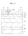
- FIG. 2 is a cross-sectional view showing the configuration of a semiconductor device (MISFET) of Comparative Example.
- the semiconductor device of Comparative Example shown in FIG. 2 is not equipped with the coupling portion VIA.
- FIG. 3 is a band diagram in the depth direction of a gate electrode portion of the semiconductor device (MISFET) of Comparative Example.
- FIG. 4 is a band diagram in the depth direction of a gate electrode portion when the gate voltage of the semiconductor device (MISFET) of First Embodiment is set at a threshold voltage and shows involvement of the two dimensional electron gas 2DEG2.
- a negative polarization charge (-opol) present at the interface between the channel layer (GaN) CH and the buffer layer (AlGaN) BU2 lifts up the potential of electrons, it is effective for suppressing a leakage current and increasing the threshold voltage.
- the buffer layer (AlGaN) BU2 has thereunder a nitride semiconductor layer (meaning the buffer layer (GaN) BU1 here) having an electron affinity smaller than that of the buffer layer (AlGaN) BU2, however, a positive polarization charge (+opol) similar in magnitude to that of the above-mentioned negative polarization charge (-opol) is present and it offsets therewith the negative polarization charge (-opol), making it impossible to achieve an expected increase in threshold voltage. In such a manner, an increase in threshold voltage is suppressed.
- An electric field EGaN extending from the side of the gate electrode GE to the negative polarization charge is therefore produced.
- the band line-up when the gate voltage Vg agrees with the threshold voltage Vth is as shown in FIG. 4 .
- Equation 1 is then substituted into Equation (2) to obtain the following rational equation (Equation 3) in which the threshold voltage Vth is a function of the electric field EGaN of the channel layer (GaN) CH.
- Vth ⁇ B + ⁇ GaN / ⁇ ox ⁇ EGaN ⁇ tox - ⁇ EC
- Equation 3 shows that with an increase in the electric field EGaN of the channel layer (GaN) CH, the threshold voltage Vth increases to the more positive side.
- Equation 3 shows that in EGaN>0, the greater the thickness tox of the gate insulating film, the higher the threshold voltage, but it is desired to form a gate insulating film having the minimum thickness satisfying a necessary gate breakdown endurance because the gate driving capacity decreases with an increase in the tox.
- the negative polarization charge causes an electric field both on the side of the gate electrode GE and on the side of the substrate S.
- a ratio of these electric fields is determined in reverse proportion to the (thickness of the buffer layer (AlGaN) BU)/(thickness of the channel layer (GaN) CH) ratio so that the thickness of the buffer layer (AlGaN) BU2 is made greater in order to enhance the threshold-voltage increasing effect.
- the buffer layer (AlGaN) BU2 is preferably made thicker than the channel layer (GaN) CH.
- the buffer layer (AlGaN) BU2 is more preferably made thicker by 10 times or more than the channel layer (GaN) CH.
- the above-mentioned two dimensional electron gas 2DEG2 is not necessarily produced in a steady state.
- generation of the two dimensional electron gas 2DEG2 until the gate voltage Vg reaches the threshold voltage Vth due to an increase in the gate voltage Vg has the threshold-voltage increasing effect.
- FIG. 5 is a cross-sectional view showing the configuration of the semiconductor device of the present embodiment.
- FIG. 6 is a plan view showing the configuration of the semiconductor device of the present embodiment.
- FIG. 5 corresponds to the cross-section A-A of FIG. 6 .
- a substrate S has thereover a nucleus formation layer NUL, a superlattice layer SL, a buffer layer BU1, a buffer layer BU2, a channel layer CH, and a barrier layer BA in order of mention.
- the barrier layer BA has thereon an insulating film IF1.
- This semiconductor device has, over the channel layer CH thereof, a gate electrode GE formed via a gate insulating film GI and a source electrode SE and a drain electrode DE formed, respectively, on both sides of the gate electrode GE.
- the gate electrode GE lies, via the gate insulating film GI, in a trench T penetrating through the insulating film IF1 and the barrier layer BA and reaching the middle of the channel layer CH.
- the gate electrode GE has thereon an interlayer insulating film IL1.
- the source electrode SE has thereunder a through-hole (also called “pore”, “hole”, or “recess”) TH.
- This through-hole TH is filled with a conductive film and configures a coupling portion VIA.
- the coupling portion VIA is coupled (ohmically coupled) to the buffer layer BU1.
- the source electrode SE and the drain electrode DE have thereon a protective film (also called “passivation film”, “insulating film”, “cover film”, or “surface protective film”) PRO.
- the substrate S has, on the back side thereof, a back surface electrode BE.
- the drain electrode DE has a rectangular planar shape having a long side in the direction Y.
- a plurality of linear drain electrodes DE are placed in the direction X with a predetermined interval.
- the source electrode SE has a rectangular planar shape having a long side in the direction Y.
- a plurality of linear source electrodes SE are placed in the direction X with a predetermined interval.
- Each of the source electrodes SE and each of the drain electrodes DE are placed alternately along the direction X
- the drain electrode DE has thereunder a contact hole C1D which will be a coupling portion between the drain electrode DE and the barrier layer BA.
- the contact hole C1d has a rectangular planar shape having a long side in the direction Y.
- the source electrode SE has thereunder a through-hole TH (coupling portion VIA).
- the through-hole TH (coupling portion VIA) has a rectangular planar shape having a long side in the direction Y.
- the drain electrode DE and the source electrode SE have therebetween a gate electrode GE.
- the gate electrode GE has a rectangular shape having a long side in the direction Y.
- the drain electrodes DE are coupled to each other via a drain pad (also called “terminal portion") DP.
- the drain pad DP is placed so as to extend in the direction X on the side of one end (on the lower side in FIG. 6 ) of the drain electrode DE.
- the drain electrodes DE are placed so as to protrude in the direction Y from the drain pad DP extending in the direction X.
- Such a shape is sometimes called "comb shape”.
- the source electrodes SE are coupled to each other via a source pad (also called “terminal portion") SP.
- the source pad SP is placed so as to extend in the direction X on the side of the other end (on the upper side in FIG. 6 ) of the source electrodes SE.
- the source electrodes SE are placed so as to protrude in the direction Y from the source pad SP extending in the direction X.
- Such a shape is sometimes called "comb shape”.
- the gate electrodes GE are coupled to each other gate via a gate line GL.
- This gate line GL is placed so as to extend in the direction X on the side of one end of the gate electrode GE (on the upper side in FIG. 6 ).
- the gate electrodes GE are placed so as to protrude in the direction Y from the gate line GL extending in the direction X.
- the gate line GL is coupled to, for example, a gate pad GP provided on both sides (only the gate pad on the right side is shown in FIG. 6 ) in the direction X of the gate line GL.
- the source electrode SE, the drain electrode DE, and the gate electrode GE are placed mainly on an active region AC surrounded with an element isolation region (ISO).
- the active region AC has a rectangular planar shape having a long side in the direction X.
- the drain pad DP, gate line GL, and the source pad SP are placed on the element isolation region (ISO).
- the active region AC and the source pad SP have therebetween the gate line GL.
- the source electrode SE has thereunder a through-hole (also called “pore”, “hole”, or “recess”) TH.
- This through-hole TH is filled with a conductive film and they configure a coupling portion VIA.
- the coupling portion VIA is coupled to the buffer layer BU1.
- the coupling portion VIA and the source pad SP, and the drain pad DP are integrated respectively with the source electrode SE and the drain electrode DE.
- the source pad SP and the drain pad DP are therefore made of the same material as that of the source electrode SE and the drain electrode DE.
- FIGS. 7 to 12 are cross-sectional views showing manufacturing steps of the semiconductor device of the present embodiment.
- a nucleus formation layer NUL and a superlattice layer L are formed on a substrate S successively.
- the substrate S for example, a semiconductor substrate made of silicon (Si) having an exposed (111) plane is used and as the nucleus formation layer NUL, for example, an aluminum nitride (AlN) layer having a thickness of about 200 nm is hetero-epitaxially grown on the substrate through metal organic chemical vapor deposition (MOCVD) or the like.
- MOCVD metal organic chemical vapor deposition
- the substrate S not only the above-mentioned silicon but also a substrate made of SiC or sapphire may be used. Further, typically, the nucleus formation layer NUL and nitride semiconductor layers (group III-V compound semiconductor layers) formed after and the nucleus formation layer NUL are all formed by the group III element plane growth (meaning gallium plane growth or aluminum plane growth in the present embodiment).
- a superlattice structure is formed as the superlattice layer SL by stacking a stacked film (AlN/GaN film) of a gallium nitride (GaN) layer and an aluminum nitride (AlN) layer in repetition.
- a gallium nitride (GaN) layer of about 20 nm thick and an aluminum nitride (AlN) layer of about 5 nm thick are hetero-epitaxially grown alternately through metal organic vapor phase deposition or the like.
- 40 layers of the stacked film are formed. This stacked film may be grown while doping with carbon (C).
- a gallium nitride layer (i-GaN layer) is hetero-epitaxially grown on the superlattice layer SL through metal organic vapor phase deposition or the like. At this time, it is grown without intentional doping with an impurity.
- the buffer layer BU1 has a thickness of, for example, about 100 nm.
- a gallium nitride layer (p-GaN layer) containing a p type impurity may be used instead.
- an AlGaN layer is hetero-epitaxially grown on the buffer layer BU1 through metal organic vapor deposition or the like. It is grown without intentional impurity doping.
- the buffer layer BU2 has a thickness of, for example, about 1000 nm.
- a channel layer CH is formed on the buffer layer BU2.
- a gallium nitride layer is hetero-epitaxially grown on the buffer layer BU2 through metal organic chemical vapor deposition or the like. At this time, it is grown without intentional impurity doping.
- the resulting channel layer CH has a film thickness of, for example, about 50 nm.
- a barrier layer BA for example, an AlGaN layer is hetero-epitaxially grown on the channel layer CH through metal organic vapor phase deposition or the like.
- Al and Ga contents are set respectively at 0.2 and 0.8 to form an Al 0.2 Ga 0.8 N layer.
- the Al content in the AlGaN layer formed as the barrier layer BA is made greater than the Al content in the AlGaN layer formed as the buffer layer BU2.
- the stacked film of the buffer layer BU1, the buffer layer BU2, the channel layer CH, and the barrier layer BA is formed.
- a two-dimensional electron gas (2DEG2) is produced in the vicinity of the interface between the buffer layer BU1 and the buffer layer BU2, while a two-dimensional electron gas (2DEG1) is produced in the vicinity of the interface between the channel layer CH and the barrier layer BA (refer to FIG. 1 ).
- a silicon nitride film of about 100 nm thick is deposited on the barrier layer BA through PECVD (plasma-enhanced chemical vapor deposition) or the like.
- a photoresist film (not illustrated) for opening an element isolation region is formed and with this photoresist film as a mask, nitrogen ions are implanted to form the element isolation region (not illustrated).
- Nitro ions are implanted to form the element isolation region (not illustrated).
- Implantation of ion species such as nitrogen (N) or boron (B) changes a crystal state and increases resistance.
- a region surrounded with the element isolation region becomes an active region AC (refer to FIG. 6 ).
- the insulating film IF1 is patterned by photolithography and etching to form an opening portion in a gate electrode formation region.
- the barrier layer BA and the channel layer CH are dry etched to form a trench T penetrating through the barrier layer BA and reaching the middle of the channel layer CH.
- a trench for gate line GL may be formed in the element isolation region (refer to FIG. 6 ).
- a gate electrode GE is formed on the insulating film IF1 and also in the trench T via a gate insulating film GI.
- a gate insulating film GI an aluminum oxide film of about 50 nm thick is deposited on the insulating film IF1 and also in the trench T through ALD (atomic layer deposition) or the like.
- a silicon oxide film or a high dielectric constant film having a dielectric constant higher than that of the silicon oxide film may be used as the gate insulating film GI.
- a hafnium-based insulating film such as HfO 2 film (hafnium oxide film), hafnium aluminate film, HfON film (hafnium oxynitride film), HfSiO film (hafnium silicate film), HfSiON film (hafnium silicon oxynitride film), or HfAlO film may be used.
- a TiN (titanium nitride) film of about 200 nm thick is formed, as a conductive film, on the gate insulating film GI by sputtering or the like.
- the TiN film is patterned by photolithography and etching to form a gate electrode GE and a gate line GL (refer to FIG. 6 ).
- the gate electrode GE may be patterned into a shape protruding on the side of a drain electrode DE which will be described later. This protruding portion is called "field plate electrode portion".
- the gate insulating film GI exposed from both sides of the gate electrode GE may be removed.
- a silicon oxide film of about 2000 nm thick is deposited as an interlayer insulating film IL1 on the gate insulating film GI and also on the gate electrode GE by PECVD or the like.
- contact holes C1S and C1D are formed in the interlayer insulating film IL1, the gate insulating film GI, and the insulating film IF1 by photolithography and etching.
- the contact holes C1S and C1D are formed in a source electrode coupling region and a drain electrode coupling region, respectively.
- a first photoresist film having an opening portion in each of the source electrode coupling region and the drain electrode coupling region is formed on the interlayer insulating film IL1.
- the interlayer insulating film IL11, the gate insulating film GI, and the insulating film IF1 are etched to form the contact holes C1S and C1D.
- the bottom surface of the contact hole C1S is etched further to form a through-hole TH.
- a second photoresist film having an opening portion in a through-hole formation region is formed on the interlayer insulating film IL1.
- the barrier layer BA, the channel layer CH, the buffer layer BU2, and a portion of the buffer layer BU1 are etched to form a through-hole TH.
- a through-hole TH penetrating through the interlayer insulating film IL1, the gate insulating film GI, the insulating film IF1, the barrier layer BA, the channel layer CH, and the buffer layer BU2 and reaching the middle of the buffer layer BU1 is formed.
- the above-mentioned etching is performed so that the through-hole TH has a bottom portion in the buffer layer BU1.
- the formation order of the contact holes C1S and C1D and the through-hole TH is not limited to the above-mentioned one. Alternatively, after formation of the through-hole TH, the contact hole C1D may be formed.
- the barrier layer BA is exposed from the bottom surface of the contact hole C1D formed in the above-mentioned step and the buffer layer BU1 is exposed from the bottom surface of the through-hole TH.
- a source electrode SE and a drain electrode DE are formed on both sides of the gate electrode GE, respectively and a coupling portion VIA is formed in the through-hole TH.
- a source pad SP to be electrically coupled to the source electrode SE is formed, while a drain pad DP to be electrically coupled to the drain electrode DE is formed (refer to FIG. 6 ).
- a conductive film is formed on the interlayer insulating film IL1 and also in the contact hole C1D and the through-hole TH.
- a stacked film (Al/TiN) made of a titanium nitride (TiN) film and an aluminum (Al) film lying thereon is formed by sputtering or the like.
- the titanium nitride film has a thickness of, for example, about 50 nm and the aluminum film has a thickness of, for example, about 1000 nm.
- a photoresist film (not illustrated) is formed in the formation regions of the source electrode SE, the drain electrode DE, the source pad SP, and the drain pad DP by photolithography.
- the conductive film Al/TiN
- a coupling portion VIA obtained by filling the through-hole TH with the conductive film is formed and also a source electrode SE, a drain electrode DE, a source pad SP, and a drain pad DP are formed.
- the source electrode SE and the drain electrode DE have, as shown in FIG. 6 , a rectangular planar shape (line shape) having a long side in the direction Y.
- the source pad SP and the drain pad DP have, as shown in FIG. 6 , a rectangular planar shape (line shape) having a long side in the direction X.
- the source pad SP is placed so as to couple a plurality of the source electrodes SE to each other, while the drain pad DP is placed so as to couple a plurality of the drain electrodes DE to each other.
- the source electrode SE has thereunder the through-hole TH and the source electrode SE and the buffer layer BU1 are electrically coupled to each other via the coupling portion VIA.
- a protective film PRO is formed on the interlayer insulating film IL1 and also on the source electrode SE, the drain electrode DE, the source pad SP, and the drain pad DP.
- a silicon oxynitride (SiON) film is deposited by CVD or the like ( FIG. 5 ).
- a stacked film (Al/TiN) made of a titanium nitride (TiN) film and an aluminum (Al) film lying thereon is deposited, as a conductive film, on the back surface of the substrate S through sputtering or the like to form a back-surface electrode BE ( FIG. 5 ).
- the semiconductor device of the present embodiment can be manufactured.
- the above-mentioned steps are however shown as one example and the semiconductor device of the present embodiment may be manufactured by steps other than the above-mentioned ones.
- a stacked portion of the buffer layer BU1 and the buffer layer BU2 having an electron affinity smaller than that of the buffer layer BU1 is provided below the channel layer CH and the coupling portion VIA reaching a position lower than the interface between these buffer layers and to be coupled to the source electrode SE is provided.
- This enables the coupling portion VIA to bring the potential of the buffer layer BU1 close to a source potential (for example, ground potential) and also enables production of a two-dimensional electron gas 2DEG2 at the interface between the buffer layer BU1 and the buffer layer BU2.
- a source potential for example, ground potential
- FIG. 13 is a graph showing the relationship, in the semiconductor device (MISFET) of the present embodiment, between an Al content of the buffer layer BU2 and a threshold voltage.
- a threshold voltage (Vth, [V]) is plotted along the ordinate and an Al content ([%]) is plotted along the abscissa.
- the threshold voltage is negative (normally-on) due to the influence of a positive fixed charge at the interface between the buffer layer (AlGaN) BU2 and the buffer layer (GaN) BU1.
- the threshold voltage increases.
- the threshold voltage exceeds "2 to 3V", that is, a threshold voltage preferable for adequate normally-off operation.
- FIG. 14 is a graph showing the relationship, in the semiconductor device (MISFET) of the present embodiment, between an Al content of the buffer layer BU2 and the on resistance.
- An on resistance (Ron, [ ⁇ mm]) is plotted along the ordinate and an Al content ([%]) is plotted along the abscissa.
- the Al content is 0%
- the on resistance is 15 ⁇ mm.
- the Al content increases, on the other hand, the on resistance increases. This is presumed to occur because with an increase in the Al content, an in-plane tensile strain of the barrier layer BA decreases and positive polarization charge at the interface between the barrier layer BA and the channel layer CH decreases, leading to a decrease in carrier concentration of the two-dimensional electron gas 2DEG1.
- the Al content is preferably 3% or more but not more than 8%, more preferably 4% or more but not more than 6%.
- the source electrode SE has thereunder the coupling portion VIA, but the source pad SP may have thereunder the coupling portion VIA.
- FIG. 15 is a cross-sectional view schematically showing the configuration of the semiconductor device of the present embodiment.
- the semiconductor device (semiconductor element) of the present embodiment is an MIS type field effect transistor using a nitride semiconductor. This semiconductor device can be used as a high electron mobility transistor (HEMT) type power transistor.
- the semiconductor device of the present embodiment is a so-called recess gate type semiconductor device.
- the semiconductor device of the present embodiment has, on a substrate S thereof, a nucleus formation layer NUL, a superlattice layer SL, a buffer layer BU1, a buffer layer BU2, a channel layer, and a barrier layer BA in order of mention.
- the MISFET of the present embodiment has, over the channel layer CH thereof, a gate electrode GE formed via a gate insulating film GI and a source electrode SE and a drain electrode DE formed respectively on both sides of the gate electrode GE.
- the gate electrode GE lies, via a gate insulating film GI, in a trench T penetrating through the barrier layer BA and reaching the middle of the channel layer CH.
- a source pad SP on an element isolation region ISO has thereunder a coupling portion VIA penetrating through the element isolation region ISO and the buffer layer BU2 and reaching the buffer layer BU1 lying thereunder.
- This coupling portion VIA is electrically coupled to the source electrode SE via the source pad SP.
- a stacked portion of the buffer layer BU1 and the buffer layer BU2 having an electron affinity smaller than that of the buffer layer BU1 is provided below the channel layer CH and the coupling portion VIA reaching a position below the interface therebetween and to be coupled to the source electrode SE is provided.
- This enables the coupling portion VIA to bring the potential of the buffer layer BU1 close to a source potential (for example, ground potential) and also enables production of a two-dimensional electron gas 2DEG at the interface between the buffer layer BU1 and the buffer layer BU2.
- a source potential for example, ground potential
- 2DEG two-dimensional electron gas
- FIG. 16 is a cross-sectional view showing the configuration of the semiconductor device of the present embodiment.
- FIG. 17 is a plan view showing the configuration of the semiconductor device of the present embodiment.
- FIG. 16 corresponds to the cross-section B-B of FIG. 17 .
- Constitutions other than the formation position of the coupling portion VIA are similar to First Embodiment so that a detailed description on the configurations similar to those of First Embodiment will be omitted.
- the semiconductor device of the present embodiment has, on a substrate S thereof, a nucleus formation layer NUL, a superlattice layer SL, a buffer layer BU1, a buffer layer BU2, a channel layer CH, and a barrier layer BA, as in First Embodiment.
- the barrier layer BA has thereon an insulating film IF1.
- the semiconductor device has, over the channel layer CH thereof, a gate electrode GE formed via a gate insulating film GI and a source electrode SE and a drain electrode DE placed on both sides of the gate electrode GE, respectively.
- the gate electrode GE lies, via the gate insulating film GI, in a trench T penetrating through the insulating film IF1 and the barrier layer BA and reaching the middle of the channel layer CH.
- the gate electrode GE has thereon an interlayer insulating film IL1.
- An element isolation region ISO is an insulating region formed in the barrier layer BA, the channel layer CH, and the buffer layer BU2 and it is a region having resistance increased, for example, by nitrogen ion implantation into a portion of the barrier layer BA, the channel layer CH, and the buffer layer BU2.
- the element isolation region ISO has, below the source pad thereon, a through-hole (also called “pore”, “hole”, or “recess”) TH.
- This through-hole TH is filled with a conductive film and they configure the coupling portion VIA. As described above, the coupling portion VIA is coupled to the buffer layer BU1.
- the source electrode SE and the drain electrode DE have thereon a protective film PRO.
- the substrate S has, on the back-surface side thereof, a back-surface electrode BE.
- a plurality of linear drain electrodes DE is placed in the direction X with a predetermined distance and a plurality of linear source electrodes SE is placed in the direction X with a predetermined distance.
- each of the source electrodes SE and each of the drain electrodes DE are placed alternately in the direction X.
- the drain electrode DE has therebelow a contact hole C1D which will be a coupling portion between the drain electrode DE and the barrier layer BA; and the source electrode SE has therebelow a contact hole C1D which will be a coupling portion between the source electrode SE and the barrier layer BA.
- the drain electrodes DE are coupled to each other by a drain pad (also called “terminal portion") DP.
- This drain pad DP is placed so as to extend in the direction X on the side of one end of the drain electrode DE (on the lower side in FIG. 17 ).
- the source electrodes SE are coupled to each other by a source pad (also called "terminal portion") SP.
- the source pad SP is placed so as to extend in the direction X on the side of the other end (on the upper side in FIG. 17 ) of the source electrodes SE.
- the gate electrodes GE are coupled to each other by a gate line GL.
- This gate line GL is placed so as to extend in the direction X on the side of one end of the gate electrode GE (on the upper side in FIG. 17 ).
- the source electrode SE, the drain electrode DE, and the gate electrode GE are placed mainly on an active region AC surrounded with the element isolation region (ISO).
- the active region AC has a rectangular planar shape having a long side in the direction X.
- the drain pad DP, gate line GL, and the source pad SP are placed on the element isolation region (ISO).
- the active region AC and the source pad SP have therebetween the gate line GL.
- the source pad SP has therebelow a through-hole (also called “pore”, “hole”, or “recess”) TH.
- This through-hole TH has therein a conductive film and they configure the coupling portion VIA.
- the coupling portion VIA is electrically coupled to the buffer layer BU1.
- the source pad SE and the buffer layer BU1 are therefore electrically coupled to each other via the source pad SP and the coupling portion VIA ( FIG. 16 ).
- Materials configuring the substrate S, the nucleus formation layer NUL, the superlattice layer SL, the buffer layer BU1, the buffer layer BU2, the channel layer CH, the barrier layer BA, and the insulating film IF1, respectively, are as described above in First Embodiment.
- Source electrode SE Materials configuring the source electrode SE, the drain electrode DE, the source pad SP, the drain pad D, and the coupling portion VIA, respectively, are as described above in First Embodiment.
- FIGS. 18 to 21 are cross-sectional views showing manufacturing steps of the semiconductor device of the present embodiment.
- a nucleus formation layer NUL and a superlattice layer SL are formed successively on a substrate S. They can be formed in a manner similar to that of First Embodiment by using the materials described in First Embodiment.
- a gallium nitride layer (i-GaN layer) is hetero-epitaxially grown on the superlattice layer SL through metal organic vapor phase deposition or the like. At this time, it is grown without intentional doping with an impurity.
- the buffer layer BU1 has a thickness of, for example, about 100 nm.
- a gallium nitride layer (p-GaN layer) containing a p type impurity may be used as the buffer layer BU1.
- an AlGaN layer is hetero-epitaxially grown on the buffer layer BU1 through metal organic vapor deposition or the like. It is grown without intentional impurity doping.
- the buffer layer BU2 has a thickness of, for example, about 1000 nm.
- a channel layer CH is formed on the buffer layer BU2.
- a gallium nitride layer is hetero-epitaxially grown on the buffer layer BU2 through metal organic chemical vapor deposition or the like. At this time, it is grown without intentional impurity doping.
- the resulting channel layer CH has a film thickness of, for example, about 50 nm.
- a barrier layer BA for example, an AlGaN layer is hetero-epitaxially grown on the channel layer CH through metal organic vapor phase deposition or the like.
- Al and Ga contents are set respectively at 0.2 and 0.8 to form an Al 0.2 Ga 0.8 N layer.
- the Al content in the AlGaN layer formed as the barrier layer BA is made greater than the Al content in the AlGaN layer formed as the buffer layer BU2.
- the stacked film of the buffer layer BU1, the buffer layer BU2, the channel layer CH, and the barrier layer BA is formed.
- a two-dimensional electron gas (2DEG2) is produced in the vicinity of the interface between the buffer layer BU1 and the buffer layer BU2, while a two-dimensional electron gas (2DEG1) is produced in the vicinity of the interface between the channel layer CH and the barrier layer BA (refer to FIG. 1 ).
- a silicon nitride film of about 100 nm thick is deposited on the barrier layer BA by PECVD or the like.
- a photoresist film (not illustrated) for opening an element isolation region is formed by photolithography.
- nitrogen ions are implanted via the insulating film IF1 to form an element isolation region.
- Implantation of ion species such as nitrogen (N) or boron (B) changes a crystal state and increases resistance.
- Implantation conditions of nitrogen ions are regulated so as to position the implantation depth, that is, the bottom portion of the element isolation region ISO below the bottom surface of the channel layer CH and at the same time, above the bottom surface of the buffer layer BU1.
- the element isolation region ISO has a bottom portion above the bottom portion of a through-hole TH (coupling portion VIA) which will be described later.
- the element isolation region ISO is formed in such a manner.
- a region surrounded with the element isolation region ISO becomes an active region AC.
- the active region AC has, for example, a substantially rectangular shape with a long side in the direction X. Then, the photoresist film is removed through release treatment with plasma.
- an opening portion is formed in a gate electrode formation region of the insulating film IF1 in a manner similar to that of First Embodiment.
- the barrier layer BA and the channel layer CH are dry etched to form a trench T penetrating through the barrier layer BA and reaching the middle of the channel layer CH.
- a trench T for gate line GL may be formed in the element isolation region ISO.
- a gate electrode GE is formed on the insulating film IF1 and also in the trench T via the gate insulating film GI.
- the insulating film IF1 and the gate electrode GE can be formed in a manner similar to that of First Embodiment by using the material described in First Embodiment.
- an interlayer insulating film IL1 is formed on the gate insulating film GI and also on the gate electrode GE in a manner similar to that of First Embodiment.
- contact holes C1S and C1D and a through-hole TH are formed in the interlayer insulating film IL1, the gate insulating film GI, and the insulating film IF1.
- a first photoresist film having an opening portion in each of a through-hole formation region, a source electrode coupling region, and a drain electrode coupling region is formed on the interlayer insulating film IL1.
- the interlayer insulating film IL1, the gate insulating film GI, and the insulating film IF1 are etched to form contact holes C1S, C1D, and C1SP.
- a second photoresist film having an opening portion on the through-hole formation region is formed on the interlayer insulating film IL1 and also in the contact holes C1S and C1D.
- the element isolation region ISO, the buffer layer BU2, and the buffer layer BU1 are etched partially to form a through-hole TH.
- a through-hole TH penetrating through the element isolation region ISO and the buffer layer BU2 and reaching the middle of the buffer layer BU1 is formed. It is to be noted that etching is performed so that the bottom portion of the through-hole TH lies in the buffer layer BU1 and at the same time, below the bottom portion of the element isolation region ISO.
- the formation order of the contact holes C1S and C1D and the through-hole TH is not limited to the above-mentioned one. Alternatively, after formation of the through-hole TH, the contact holes C1S and C1D may be formed.
- the barrier layer BA is exposed from the bottom surface of the contact holes C1S and C1D formed in the above-mentioned step and the buffer layer BU1 is exposed from the bottom surface of the through-hole TH.
- a source electrode SE, a drain electrode DE, a source pad SP, a drain pad PD, and a coupling portion VIA are formed by forming a conductive film on the interlayer insulating film IL1 and also in the contact holes C1S and C1D and the through-hole TH. They can be formed in a manner similar to that of First Embodiment by using the materials described in First Embodiment.
- a protective film PRO is formed on the interlayer insulating film IL1 and also on the source electrode SE, the drain electrode DE, the source pad SP, and the drain pad DP ( FIG. 16 ).
- the back surface of the substrate S is polished to thin the substrate S.
- a stacked film (Al/TiN) made of a titanium nitride (TiN) film and an aluminum (Al) film lying thereon is deposited, as a conductive film, on the back surface of the substrate S by sputtering or the like to form a back-surface electrode BE ( FIG. 16 ).
- the semiconductor device of the present embodiment can be manufactured.
- the above-mentioned steps are however shown as one example and the semiconductor device of the present embodiment may be manufactured by steps other than the above-mentioned steps.
- the coupling portion VIA is provided on the surface side of the substrate S, but the coupling portion VIA may be provided on the back surface side of the substrate S.
- FIG. 22 is a cross-sectional view schematically showing the configuration of the semiconductor device of the present embodiment.
- the semiconductor device (semiconductor element) of the present embodiment is an MIS type field effect transistor using a nitride semiconductor. This semiconductor device can be used as a high electron mobility transistor (HEMT) type power transistor.
- the semiconductor device of the present embodiment is a so-called recess gate type semiconductor device.
- the semiconductor device of the present embodiment has, on a substrate S thereof, a nucleus formation layer NUL, a superlattice layer SL, a buffer layer BU1, a buffer layer BU2, a channel layer, and a barrier layer BA in order of mention.
- the MISFET of the present embodiment has, over the channel layer CH thereof, a gate electrode GE formed via a gate insulating film GI and a source electrode SE and a drain electrode DE formed respectively on both sides of the gate electrode GE.
- the gate electrode GE lies, via the gate insulating fil GI, in a trench T penetrating through the barrier layer BA and reaching the middle of the channel layer CH.
- the semiconductor device of the present embodiment is provided with a coupling portion VIA starting from the back surface of the substrate S, penetrating through the substrate S, the nucleus formation layer NUL, and the superlattice layer SL, and reaching the buffer layer BU1.
- This coupling portion VIA is electrically coupled to a source potential (for example, ground potential) via the back surface electrode BE.
- a stacked portion of the buffer layer BU1 and the buffer layer BU2 having an electron affinity smaller than that of the buffer layer BU1 is provided below the channel layer CH and the coupling portion VIA starting from the back surface of the substrate S and reaching the buffer layer BU1 is provided.
- This enables the coupling portion VIA to bring the potential of the buffer layer BU1 close to a source potential (for example, ground potential) and also enables production of a two-dimensional electron gas 2DEG at the interface between the buffer layer BU1 and the buffer layer BU2.
- a source potential for example, ground potential
- 2DEG two-dimensional electron gas
- FIG. 23 is a cross-sectional view showing the configuration of the semiconductor device of the present embodiment.
- FIG. 24 is a plan view showing the configuration of the semiconductor device of the present embodiment.
- FIG. 23 corresponds to the cross-section C-C of FIG. 24 .
- Constitutions other than the formation position of the coupling portion VIA are similar to Second Embodiment so that a detailed description on the configurations similar to those of Second Embodiment will be omitted.
- the semiconductor device of the present embodiment has, on a substrate S thereof, a nucleus formation layer NUL, a superlattice layer SL, a buffer layer BU1, a buffer layer BU2, a channel layer CH, and a barrier layer BA in order of mention, as in First Embodiment.
- the barrier layer BA has thereon an insulating film IF1.
- the semiconductor device has, over the channel layer CH thereof, a gate electrode GE formed via a gate insulating film GI and a source electrode SE and a drain electrode DE placed on both sides of the gate electrode GE, respectively.
- the gate electrode GE lies, via the gate insulating film GI, in a trench T penetrating through the insulating film IF1 and the barrier layer BA and reaching the middle of the channel layer CH.
- the gate electrode GE has thereon an interlayer insulating film IL1.
- the source electrode SE and the drain electrode DE have thereon a protective film PRO.
- a coupling portion VIA starting from the back surface of the substrate S, penetrating through the substrate S, the nucleus formation layer NUL, and the superlattice layer SL, and reaching the buffer layer BU1 is provided.
- the substrate S has, on the back surface thereof, a back-surface electrode BE.
- the coupling portion VIA is coupled to the buffer layer BU1 and is electrically coupled to a source potential (for example, ground potential) via the back-surface electrode BE.
- a plurality of linear drain electrodes DE is placed in the direction X with a predetermined distance, while a plurality of linear source electrodes SE is placed in the direction X with a predetermined distance.
- each of the source electrodes SE and each of the drain electrodes DE is placed alternately along the direction X.
- the drain electrode DE has therebelow a contact hole C1D which will be a coupling portion between the drain electrode DE and the barrier layer BA.
- the source electrode SE has therebelow a contact hole C1S which will be a coupling portion between the source electrode SE and the barrier layer BA.
- the drain electrodes DE are coupled to each other by a drain pad (also called “terminal portion") DP, while the source electrodes SE are coupled to each other by a source pad (also called “terminal portion”) SP.
- the gate electrodes GE are coupled to each other by a gate line GL. This gate line GL is placed so as to extend in the direction X on the side of one end of the gate electrode GE (on the upper side in FIG. 24 ).
- a through-hole also called “pore”, “hole”, or “recess”
- the through-hole TH is however provided on the back surface side of the substrate S as shown in FIG. 23 .
- This coupling portion VIA is electrically coupled to a source potential (for example, ground potential) via the back-surface electrode BE.
- a source potential for example, ground potential
- the through-hole TH (circle portion) is placed at a position corresponding to the source electrode SE but the position of the through-hole TH (circle portion) is not limited to it.
- the through-hole TH (circle portion) is provided on the back surface side of the substrate S so that it can be laid out freely without being limited by a pattern layout on the surface side.
- Materials configuring the substrate S, the nucleus formation layer NUL, the superlattice layer SL, the buffer layer BU1, the buffer layer BU2, the channel layer CH, the barrier layer BA, and the insulating film IF1, respectively, are as described above in First Embodiment.
- the source electrode SE, the drain electrode DE, the source pad SP, the drain pad DP, and the coupling portion VIA (back-surface electrode BE), respectively, are as described above in First Embodiment.
- the source electrode SE, the drain electrode DE, the source pad SP, and the drain pad DP may be made of a material different from a material configuring the coupling portion VIA (back-surface electrode BE).
- FIGS. 25 to 28 are cross-sectional views showing manufacturing steps of the semiconductor device of the present embodiment.
- a nucleus formation layer NUL, a superlattice layer SL, a buffer layer BU1, a buffer layer BU2, a channel layer CH, and a barrier layer BA are formed successively on a substrate S. They can be formed in a manner similar to that of First Embodiment or Second Embodiment by using the materials as described in First Embodiment or Second Embodiment. Next, as in First Embodiment or Second Embodiment, an insulating film IF1 is formed on the barrier layer BA.
- a photoresist film (not illustrated) for opening an element isolation region is formed and with this photoresist film as a mask, nitrogen ions are implanted to form the element isolation region (not illustrated).
- a trench T penetrating through the barrier layer BA and reaching the middle of the channel layer CH is formed.
- a gate electrode GE is formed in this trench T via the gate insulating film GI.
- an interlayer insulating film IL1 is formed on the gate electrode GE and then, contact holes C1S and C1D are formed in the interlayer insulating film IL1, the gate insulating film GI, and the insulating film IF1.
- a photoresist film (not illustrated) having opening portions in a source electrode coupling region and a drain electrode coupling region, respectively, is formed on the interlayer insulating film IL1. Then, with this photoresist film as a mask, the interlayer insulating film IL1, the gate insulating film GI, and the insulating film IF1 are etched to form contact holes C1S and C1D. The barrier layer BA is exposed from the bottom surface of these contact holes C1S and C1D.
- a source electrode SE, a drain electrode DE, a source pad SP, and a drain pad DP are formed by forming a conductive film on the interlayer insulating film IL1 and also in the contact holes C1S and C1D. They can be formed as in First Embodiment by using a material described above in First Embodiment.
- a protective film PRO is formed on the interlayer insulating film IL1 and also on the source electrode SE, the drain electrode DE, the source pad SP, and the drain pad DP.
- a mask film (not illustrated) having an opening portion in a through-hole formation region is formed on the back surface of the substrate S and with this mask film as a mask, the substrate S, the nucleus formation layer NUL, the superlattice layer SL, and the buffer layer BU1 are partially etched to form a through-hole TH.
- a through-hole TH penetrating through the substrate S, the nucleus formation layer NUL, and the superlattice layer SL and reaching the buffer layer BU1 lying thereunder is formed.
- a conductive film is formed on the back surface side of the substrate S and also in the through-hole TH. It is formed, for example, through sputtering or the like by using, as the conductive film, a stacked film (Al/TiN) made of a titanium nitride (TiN) film and an aluminum (Al) film lying thereon.
- the through-hole TH is therefore filled with the conductive film and a coupling portion VIA is formed.
- a back-surface electrode BE is formed from the conductive film deposited on the back surface of the substrate S.
- the coupling portion VIA is coupled to the back-surface electrode BE and, for example, a ground potential (source potential) is applied to the back-surface electrode BE.
- the semiconductor device of the present embodiment can be manufactured.
- the above-mentioned steps are however shown as one example and the semiconductor device of the present embodiment may be manufactured by steps other than the above-mentioned steps.
- the bottom surface of the coupling portion VIA is placed in the middle of the buffer layer BU1, but the bottom surface of the coupling portion VIA may be placed below the bottom surface of the buffer layer BU1.
- FIG. 29 is a cross-sectional view showing another configuration of First Embodiment.
- the configuration other than the coupling portion VIA is similar to First Embodiment, so that a description on it is omitted.
- the bottom surface of the coupling portion VIA may be placed below the bottom surface of the buffer layer BU1 to bring a portion of the side surface of the coupling portion VIA into contact with the buffer layer BU1.
- the coupling portion VIA is formed, for example, by forming a through-hole TH penetrating through the barrier layer BA, the channel layer CH, the buffer layer BU2, and the buffer layer BU1 and reaching the middle of the superlattice layer SL and then filling the through-hole TH with a conductive film.
- the bottom surface of the coupling portion VIA of Second Embodiment may be placed below the bottom surface of the buffer layer BU1.
- a GaN layer and an AlGaN layer are given as examples of a nitride semiconductor layer configuring the buffer layer BU1, the buffer layer BU2, the channel layer CH, and the barrier layer BA, but another nitride semiconductor layer may be used.
- the GaN layer may be replaced by an InGaN layer or the AlGaN layer may be replaced by an InAlN layer.
- the semiconductor element (MISFET) described in the above-mentioned embodiments can be used as a semiconductor element (MISFET) configuring a switched-mode power supply, a PFC circuit, or an inverter.
- a switched-mode power supply examples include a server power supply, an interruptible power supply, a power conditioner for photovoltaic generation, and HV ⁇ EV power supply.
- products using a PFC circuit include various industrial power supplies such as server and motor, domestic power supplies, and adapter power supplies for various mobile devices.
- Examples of products using an inverter include motor drive power supplies and plug-in HV power supplies.
Applications Claiming Priority (1)
| Application Number | Priority Date | Filing Date | Title |
|---|---|---|---|
| JP2014021247A JP6341679B2 (ja) | 2014-02-06 | 2014-02-06 | 半導体装置 |
Publications (2)
| Publication Number | Publication Date |
|---|---|
| EP2913853A2 true EP2913853A2 (de) | 2015-09-02 |
| EP2913853A3 EP2913853A3 (de) | 2016-03-02 |
Family
ID=52232111
Family Applications (1)
| Application Number | Title | Priority Date | Filing Date |
|---|---|---|---|
| EP15150397.6A Withdrawn EP2913853A3 (de) | 2014-02-06 | 2015-01-08 | Halbleiterbauelement |
Country Status (6)
| Country | Link |
|---|---|
| US (1) | US9306051B2 (de) |
| EP (1) | EP2913853A3 (de) |
| JP (1) | JP6341679B2 (de) |
| KR (1) | KR20150093117A (de) |
| CN (1) | CN104835847B (de) |
| TW (1) | TWI625796B (de) |
Cited By (1)
| Publication number | Priority date | Publication date | Assignee | Title |
|---|---|---|---|---|
| CN112864015A (zh) * | 2021-01-27 | 2021-05-28 | 浙江集迈科微电子有限公司 | GaN器件及制备方法 |
Families Citing this family (20)
| Publication number | Priority date | Publication date | Assignee | Title |
|---|---|---|---|---|
| JP6534791B2 (ja) | 2013-12-16 | 2019-06-26 | ルネサスエレクトロニクス株式会社 | 半導体装置 |
| JP6565223B2 (ja) | 2015-03-05 | 2019-08-28 | 富士通株式会社 | 半導体装置及びその製造方法、電源装置、高周波増幅器 |
| JP6462456B2 (ja) * | 2015-03-31 | 2019-01-30 | ルネサスエレクトロニクス株式会社 | 半導体装置および半導体装置の製造方法 |
| ITUB20155862A1 (it) * | 2015-11-24 | 2017-05-24 | St Microelectronics Srl | Transistore di tipo normalmente spento con ridotta resistenza in stato acceso e relativo metodo di fabbricazione |
| TWI611505B (zh) * | 2016-06-02 | 2018-01-11 | 世界先進積體電路股份有限公司 | 溝槽隔離結構及其製造方法 |
| US10347524B2 (en) | 2016-09-12 | 2019-07-09 | Vanguard International Semiconductor Corporation | Trench isolation structures and methods for forming the same |
| DE102016122399A1 (de) * | 2016-11-21 | 2018-05-24 | Forschungsverbund Berlin E.V. | Gate-Struktur und Verfahren zu dessen Herstellung |
| IT201700064147A1 (it) * | 2017-06-09 | 2018-12-09 | St Microelectronics Srl | Transistore hemt normalmente spento con generazione selettiva del canale 2deg e relativo metodo di fabbricazione |
| TWI793076B (zh) * | 2017-06-30 | 2023-02-21 | 晶元光電股份有限公司 | 半導體元件 |
| WO2019009111A1 (ja) * | 2017-07-07 | 2019-01-10 | パナソニックIpマネジメント株式会社 | 半導体装置およびその製造方法 |
| TWI637515B (zh) * | 2017-07-12 | 2018-10-01 | 世界先進積體電路股份有限公司 | 高電子遷移率電晶體元件 |
| JP2019050232A (ja) * | 2017-09-07 | 2019-03-28 | ルネサスエレクトロニクス株式会社 | 半導体装置の製造方法および半導体装置 |
| US10325990B2 (en) | 2017-10-03 | 2019-06-18 | Vanguard International Semiconductor Corporation | High electron mobility transistor devices and method for fabricating the same |
| US11489061B2 (en) * | 2018-09-24 | 2022-11-01 | Intel Corporation | Integrated programmable gate radio frequency (RF) switch |
| US11387328B2 (en) * | 2018-09-27 | 2022-07-12 | Intel Corporation | III-N tunnel device architectures and high frequency mixers employing a III-N tunnel device |
| CN111354789B (zh) * | 2018-12-24 | 2023-11-07 | 苏州捷芯威半导体有限公司 | 半导体器件及制作方法 |
| CN111987156A (zh) * | 2020-08-31 | 2020-11-24 | 厦门市三安集成电路有限公司 | 氮化镓基晶体管器件外延结构及其制备方法、器件 |
| US20220199822A1 (en) | 2020-12-18 | 2022-06-23 | Innoscience (Suzhou) Technology Co., Ltd. | Semiconductor device and method for manufacturing the same |
| CN115966605A (zh) * | 2020-12-18 | 2023-04-14 | 英诺赛科(苏州)科技有限公司 | 半导体器件 |
| US20230078017A1 (en) * | 2021-09-16 | 2023-03-16 | Wolfspeed, Inc. | Semiconductor device incorporating a substrate recess |
Citations (3)
| Publication number | Priority date | Publication date | Assignee | Title |
|---|---|---|---|---|
| JP2007103451A (ja) | 2005-09-30 | 2007-04-19 | Toshiba Corp | 半導体装置及びその製造方法 |
| JP2009009993A (ja) | 2007-06-26 | 2009-01-15 | Toshiba Corp | 半導体装置 |
| JP2009200096A (ja) | 2008-02-19 | 2009-09-03 | Sharp Corp | 窒化物半導体装置とそれを含む電力変換装置 |
Family Cites Families (20)
| Publication number | Priority date | Publication date | Assignee | Title |
|---|---|---|---|---|
| US20050145851A1 (en) | 2003-12-17 | 2005-07-07 | Nitronex Corporation | Gallium nitride material structures including isolation regions and methods |
| JP2006196869A (ja) * | 2004-12-13 | 2006-07-27 | Matsushita Electric Ind Co Ltd | 半導体装置及びその製造方法 |
| JP2007128994A (ja) * | 2005-11-02 | 2007-05-24 | New Japan Radio Co Ltd | 半導体装置 |
| JP4967708B2 (ja) * | 2007-02-27 | 2012-07-04 | 富士通株式会社 | 化合物半導体装置及びそれを用いたドハティ増幅器 |
| JP2009026975A (ja) * | 2007-07-20 | 2009-02-05 | Toshiba Corp | 半導体装置 |
| US7795642B2 (en) * | 2007-09-14 | 2010-09-14 | Transphorm, Inc. | III-nitride devices with recessed gates |
| JP5809802B2 (ja) * | 2008-03-12 | 2015-11-11 | ルネサスエレクトロニクス株式会社 | 半導体装置 |
| JP2009231508A (ja) * | 2008-03-21 | 2009-10-08 | Panasonic Corp | 半導体装置 |
| JP5468768B2 (ja) * | 2008-12-05 | 2014-04-09 | パナソニック株式会社 | 電界効果トランジスタ及びその製造方法 |
| JP2010135640A (ja) * | 2008-12-05 | 2010-06-17 | Panasonic Corp | 電界効果トランジスタ |
| KR101774933B1 (ko) * | 2010-03-02 | 2017-09-06 | 삼성전자 주식회사 | 듀얼 디플리션을 나타내는 고 전자 이동도 트랜지스터 및 그 제조방법 |
| JP5611653B2 (ja) * | 2010-05-06 | 2014-10-22 | 株式会社東芝 | 窒化物半導体素子 |
| TWI587512B (zh) * | 2011-05-16 | 2017-06-11 | Renesas Electronics Corp | Field effect transistor and semiconductor device |
| US9087812B2 (en) * | 2011-07-15 | 2015-07-21 | International Rectifier Corporation | Composite semiconductor device with integrated diode |
| US8674372B2 (en) * | 2011-08-19 | 2014-03-18 | Infineon Technologies Austria Ag | HEMT with integrated low forward bias diode |
| JP5654512B2 (ja) * | 2012-03-26 | 2015-01-14 | 株式会社東芝 | 窒化物半導体装置 |
| JP5895666B2 (ja) * | 2012-03-30 | 2016-03-30 | 富士通株式会社 | 化合物半導体装置及びその製造方法 |
| JP6214978B2 (ja) * | 2013-09-17 | 2017-10-18 | 株式会社東芝 | 半導体装置 |
| JP6534791B2 (ja) * | 2013-12-16 | 2019-06-26 | ルネサスエレクトロニクス株式会社 | 半導体装置 |
| JP6251071B2 (ja) * | 2014-02-05 | 2017-12-20 | ルネサスエレクトロニクス株式会社 | 半導体装置 |
-
2014
- 2014-02-06 JP JP2014021247A patent/JP6341679B2/ja active Active
-
2015
- 2015-01-06 US US14/590,433 patent/US9306051B2/en not_active Expired - Fee Related
- 2015-01-08 EP EP15150397.6A patent/EP2913853A3/de not_active Withdrawn
- 2015-01-29 TW TW104102935A patent/TWI625796B/zh active
- 2015-02-03 KR KR1020150016615A patent/KR20150093117A/ko not_active Application Discontinuation
- 2015-02-06 CN CN201510065057.4A patent/CN104835847B/zh active Active
Patent Citations (3)
| Publication number | Priority date | Publication date | Assignee | Title |
|---|---|---|---|---|
| JP2007103451A (ja) | 2005-09-30 | 2007-04-19 | Toshiba Corp | 半導体装置及びその製造方法 |
| JP2009009993A (ja) | 2007-06-26 | 2009-01-15 | Toshiba Corp | 半導体装置 |
| JP2009200096A (ja) | 2008-02-19 | 2009-09-03 | Sharp Corp | 窒化物半導体装置とそれを含む電力変換装置 |
Cited By (2)
| Publication number | Priority date | Publication date | Assignee | Title |
|---|---|---|---|---|
| CN112864015A (zh) * | 2021-01-27 | 2021-05-28 | 浙江集迈科微电子有限公司 | GaN器件及制备方法 |
| CN112864015B (zh) * | 2021-01-27 | 2022-07-05 | 浙江集迈科微电子有限公司 | GaN器件及制备方法 |
Also Published As
| Publication number | Publication date |
|---|---|
| TW201546911A (zh) | 2015-12-16 |
| US20150221758A1 (en) | 2015-08-06 |
| JP2015149392A (ja) | 2015-08-20 |
| JP6341679B2 (ja) | 2018-06-13 |
| CN104835847B (zh) | 2020-02-28 |
| EP2913853A3 (de) | 2016-03-02 |
| TWI625796B (zh) | 2018-06-01 |
| CN104835847A (zh) | 2015-08-12 |
| KR20150093117A (ko) | 2015-08-17 |
| US9306051B2 (en) | 2016-04-05 |
Similar Documents
| Publication | Publication Date | Title |
|---|---|---|
| US9306051B2 (en) | Semiconductor device using a nitride semiconductor | |
| US10084077B2 (en) | Semiconductor device and method of manufacturing semiconductor device | |
| US9853108B2 (en) | Nitride semiconductor device using insulating films having different bandgaps to enhance performance | |
| US10256100B2 (en) | Manufacturing method of semiconductor device and semiconductor device | |
| US9620599B2 (en) | GaN-based semiconductor transistor | |
| US10256333B2 (en) | High electron mobility transistor | |
| US8963207B2 (en) | Semiconductor device | |
| KR20150092708A (ko) | 반도체 장치 | |
| US9978642B2 (en) | III-V nitride semiconductor device having reduced contact resistance | |
| US10679860B2 (en) | Self-aligning source, drain and gate process for III-V nitride MISHEMTs | |
| US9825139B2 (en) | Semiconductor device and method | |
| US9653591B2 (en) | Compound semiconductor device having at least one buried semiconductor material region | |
| JP2018174196A (ja) | 半導体装置および半導体装置の製造方法 | |
| US8835985B2 (en) | Power electronic device and method of manufacturing the same | |
| CN110010680A (zh) | 半导体装置及半导体结构 |
Legal Events
| Date | Code | Title | Description |
|---|---|---|---|
| PUAI | Public reference made under article 153(3) epc to a published international application that has entered the european phase |
Free format text: ORIGINAL CODE: 0009012 |
|
| AK | Designated contracting states |
Kind code of ref document: A2 Designated state(s): AL AT BE BG CH CY CZ DE DK EE ES FI FR GB GR HR HU IE IS IT LI LT LU LV MC MK MT NL NO PL PT RO RS SE SI SK SM TR |
|
| AX | Request for extension of the european patent |
Extension state: BA ME |
|
| RAP1 | Party data changed (applicant data changed or rights of an application transferred) |
Owner name: RENESAS ELECTRONICS CORPORATION |
|
| PUAL | Search report despatched |
Free format text: ORIGINAL CODE: 0009013 |
|
| AK | Designated contracting states |
Kind code of ref document: A3 Designated state(s): AL AT BE BG CH CY CZ DE DK EE ES FI FR GB GR HR HU IE IS IT LI LT LU LV MC MK MT NL NO PL PT RO RS SE SI SK SM TR |
|
| AX | Request for extension of the european patent |
Extension state: BA ME |
|
| RIC1 | Information provided on ipc code assigned before grant |
Ipc: H01L 29/417 20060101ALI20160128BHEP Ipc: H01L 29/20 20060101ALN20160128BHEP Ipc: H01L 21/336 20060101ALI20160128BHEP Ipc: H01L 29/423 20060101ALN20160128BHEP Ipc: H01L 29/10 20060101ALI20160128BHEP Ipc: H01L 29/778 20060101AFI20160128BHEP |
|
| 17P | Request for examination filed |
Effective date: 20160902 |
|
| RBV | Designated contracting states (corrected) |
Designated state(s): AL AT BE BG CH CY CZ DE DK EE ES FI FR GB GR HR HU IE IS IT LI LT LU LV MC MK MT NL NO PL PT RO RS SE SI SK SM TR |
|
| 17Q | First examination report despatched |
Effective date: 20170803 |
|
| STAA | Information on the status of an ep patent application or granted ep patent |
Free format text: STATUS: THE APPLICATION IS DEEMED TO BE WITHDRAWN |
|
| 18D | Application deemed to be withdrawn |
Effective date: 20200807 |