EP2908348B1 - Dünnfilmtransistor und dessen herstellungsverfahren, arraysubstrat und anzeigevorrichtung - Google Patents
Dünnfilmtransistor und dessen herstellungsverfahren, arraysubstrat und anzeigevorrichtung Download PDFInfo
- Publication number
- EP2908348B1 EP2908348B1 EP14856040.2A EP14856040A EP2908348B1 EP 2908348 B1 EP2908348 B1 EP 2908348B1 EP 14856040 A EP14856040 A EP 14856040A EP 2908348 B1 EP2908348 B1 EP 2908348B1
- Authority
- EP
- European Patent Office
- Prior art keywords
- active region
- semiconductor active
- charge transfer
- thin film
- surface charge
- Prior art date
- Legal status (The legal status is an assumption and is not a legal conclusion. Google has not performed a legal analysis and makes no representation as to the accuracy of the status listed.)
- Active
Links
Images


Classifications
-
- H—ELECTRICITY
- H10—SEMICONDUCTOR DEVICES; ELECTRIC SOLID-STATE DEVICES NOT OTHERWISE PROVIDED FOR
- H10D—INORGANIC ELECTRIC SEMICONDUCTOR DEVICES
- H10D30/00—Field-effect transistors [FET]
- H10D30/60—Insulated-gate field-effect transistors [IGFET]
- H10D30/67—Thin-film transistors [TFT]
- H10D30/6757—Thin-film transistors [TFT] characterised by the structure of the channel, e.g. transverse or longitudinal shape or doping profile
-
- H—ELECTRICITY
- H10—SEMICONDUCTOR DEVICES; ELECTRIC SOLID-STATE DEVICES NOT OTHERWISE PROVIDED FOR
- H10D—INORGANIC ELECTRIC SEMICONDUCTOR DEVICES
- H10D30/00—Field-effect transistors [FET]
- H10D30/60—Insulated-gate field-effect transistors [IGFET]
- H10D30/67—Thin-film transistors [TFT]
- H10D30/6704—Thin-film transistors [TFT] having supplementary regions or layers in the thin films or in the insulated bulk substrates for controlling properties of the device
-
- H—ELECTRICITY
- H10—SEMICONDUCTOR DEVICES; ELECTRIC SOLID-STATE DEVICES NOT OTHERWISE PROVIDED FOR
- H10D—INORGANIC ELECTRIC SEMICONDUCTOR DEVICES
- H10D30/00—Field-effect transistors [FET]
- H10D30/60—Insulated-gate field-effect transistors [IGFET]
- H10D30/67—Thin-film transistors [TFT]
- H10D30/674—Thin-film transistors [TFT] characterised by the active materials
- H10D30/6755—Oxide semiconductors, e.g. zinc oxide, copper aluminium oxide or cadmium stannate
-
- H—ELECTRICITY
- H10—SEMICONDUCTOR DEVICES; ELECTRIC SOLID-STATE DEVICES NOT OTHERWISE PROVIDED FOR
- H10D—INORGANIC ELECTRIC SEMICONDUCTOR DEVICES
- H10D62/00—Semiconductor bodies, or regions thereof, of devices having potential barriers
- H10D62/10—Shapes, relative sizes or dispositions of the regions of the semiconductor bodies; Shapes of the semiconductor bodies
-
- H—ELECTRICITY
- H10—SEMICONDUCTOR DEVICES; ELECTRIC SOLID-STATE DEVICES NOT OTHERWISE PROVIDED FOR
- H10D—INORGANIC ELECTRIC SEMICONDUCTOR DEVICES
- H10D62/00—Semiconductor bodies, or regions thereof, of devices having potential barriers
- H10D62/80—Semiconductor bodies, or regions thereof, of devices having potential barriers characterised by the materials
-
- H—ELECTRICITY
- H10—SEMICONDUCTOR DEVICES; ELECTRIC SOLID-STATE DEVICES NOT OTHERWISE PROVIDED FOR
- H10D—INORGANIC ELECTRIC SEMICONDUCTOR DEVICES
- H10D62/00—Semiconductor bodies, or regions thereof, of devices having potential barriers
- H10D62/80—Semiconductor bodies, or regions thereof, of devices having potential barriers characterised by the materials
- H10D62/86—Semiconductor bodies, or regions thereof, of devices having potential barriers characterised by the materials being Group II-VI materials, e.g. ZnO
-
- H—ELECTRICITY
- H10—SEMICONDUCTOR DEVICES; ELECTRIC SOLID-STATE DEVICES NOT OTHERWISE PROVIDED FOR
- H10D—INORGANIC ELECTRIC SEMICONDUCTOR DEVICES
- H10D86/00—Integrated devices formed in or on insulating or conducting substrates, e.g. formed in silicon-on-insulator [SOI] substrates or on stainless steel or glass substrates
- H10D86/01—Manufacture or treatment
- H10D86/021—Manufacture or treatment of multiple TFTs
- H10D86/0221—Manufacture or treatment of multiple TFTs comprising manufacture, treatment or patterning of TFT semiconductor bodies
-
- H—ELECTRICITY
- H10—SEMICONDUCTOR DEVICES; ELECTRIC SOLID-STATE DEVICES NOT OTHERWISE PROVIDED FOR
- H10D—INORGANIC ELECTRIC SEMICONDUCTOR DEVICES
- H10D86/00—Integrated devices formed in or on insulating or conducting substrates, e.g. formed in silicon-on-insulator [SOI] substrates or on stainless steel or glass substrates
- H10D86/40—Integrated devices formed in or on insulating or conducting substrates, e.g. formed in silicon-on-insulator [SOI] substrates or on stainless steel or glass substrates characterised by multiple TFTs
- H10D86/421—Integrated devices formed in or on insulating or conducting substrates, e.g. formed in silicon-on-insulator [SOI] substrates or on stainless steel or glass substrates characterised by multiple TFTs having a particular composition, shape or crystalline structure of the active layer
- H10D86/423—Integrated devices formed in or on insulating or conducting substrates, e.g. formed in silicon-on-insulator [SOI] substrates or on stainless steel or glass substrates characterised by multiple TFTs having a particular composition, shape or crystalline structure of the active layer comprising semiconductor materials not belonging to the Group IV, e.g. InGaZnO
-
- H—ELECTRICITY
- H10—SEMICONDUCTOR DEVICES; ELECTRIC SOLID-STATE DEVICES NOT OTHERWISE PROVIDED FOR
- H10D—INORGANIC ELECTRIC SEMICONDUCTOR DEVICES
- H10D86/00—Integrated devices formed in or on insulating or conducting substrates, e.g. formed in silicon-on-insulator [SOI] substrates or on stainless steel or glass substrates
- H10D86/40—Integrated devices formed in or on insulating or conducting substrates, e.g. formed in silicon-on-insulator [SOI] substrates or on stainless steel or glass substrates characterised by multiple TFTs
- H10D86/60—Integrated devices formed in or on insulating or conducting substrates, e.g. formed in silicon-on-insulator [SOI] substrates or on stainless steel or glass substrates characterised by multiple TFTs wherein the TFTs are in active matrices
-
- H—ELECTRICITY
- H10—SEMICONDUCTOR DEVICES; ELECTRIC SOLID-STATE DEVICES NOT OTHERWISE PROVIDED FOR
- H10D—INORGANIC ELECTRIC SEMICONDUCTOR DEVICES
- H10D99/00—Subject matter not provided for in other groups of this subclass
Definitions
- the present invention relates to the technical field of manufacturing technology of display apparatus, and particularly relates to a thin film transistor and a manufacturing method thereof, an array substrate, and a display apparatus.
- impurity ions are generally doped into a semiconductor active region of the thin film transistor so that the semiconductor active region is converted into a P-doped or N-doped semiconductor active region, thereby lifetime of carriers in the semiconductor active region is longer, mobility of the carriers is higher, and the performance of the thin film transistor is improved.
- Ion implantation doping method is used for semiconductor doping. Ion implantation is performed by accelerating impurity ions in a vacuum and low temperature environment so that the impurity ions obtaining large kinetic energy may directly enter into material of the semiconductor active region, thus the semiconductor active region is converted into a doped semiconductor active region, meanwhile, integrity and periodicity of lattices of the material of the semiconductor active region itself may also be destroyed, resulting in the fact that some lattice defects may occur in the semiconductor active region, lifetime and mobility of the carriers are affected, and improvement of performance of the thin film transistor is limited.
- FR2537781A1 relates to a field-effect transistor with two-dimensional electron gas, known by the name of TEGFET.
- the two-dimensional electron gas forms near the heterojunction, inside the active layer, and electrical access thereto is through electrically resistant layers.
- the transistor according to the invention includes a semi-insulating substrate 13, a n ⁇ -> doped active layer 14 and a n ⁇ -> doped gate layer 15: the two-dimensional electron gas forms at the heterojunction 18 between these two layers 14, 15.
- two compartments 19, 20 of the same material as the active layer 14 but n ⁇ +> doped are interposed between the active layer 14 and the gate layer 15: they are therefore in direct contact with the electron gas.; Moreover, the two metallisations 21, 22 of source and drain penetrate through the surface layer(s) 15, 16 to the interior of the compartments 19, 20 and are also in direct contact with the electron gas.
- transistors for microwave frequencies of the order of 50 GHz.
- US20120211705A1 is to provide a device capable of having an easy production process and achieving a long lifetime.
- a device comprising a substrate, two or more electrodes facing each other disposed on the substrate and a positive hole injection transport layer disposed between two electrodes among the two or more electrodes, wherein the positive hole injection transport layer comprises a transition metal-containing nanoparticle containing at least a transition metal compound including a transition metal oxide, a transition metal and a protecting agent, or at least the transition metal compound including the transition metal oxide, and the protecting agent.
- US20110297217A1 provides a recombination layer with a gradient work function, which increases the power-conversion efficiency of multijunction photovoltaic devices by reducing the energy barrier to charge carriers migrating between pairs of photovoltaic junctions thereby facilitating the optimal recombination of opposing electron and hole currents generated when the photovoltaic is illuminated.
- an object of the present invention is to provide an improved thin film transistor and a manufacturing method thereof, an array substrate, and a display apparatus.
- the present invention provides a thin film transistor, comprising a gate, a gate insulation layer, a semiconductor active region, and a source and a drain connected with the semiconductor active region, the thin film transistor further comprises a surface charge transfer layer in contact with the semiconductor active region, the surface charge transfer layer is located above or below the semiconductor active region, and is used for causing the semiconductor active region to generate a large number of holes therein without changing the lattice structure of the semiconductor active region.
- the energy level difference between the lowest unoccupied molecular orbit of material of the surface charge transfer layer and the top of valence band of material of the semiconductor active region is greater than or equal to -1eV and less than or equal to 1eV.
- the gate is provided on a base, the gate insulation layer covers the gate, the surface charge transfer layer is provided above the gate insulation layer, and the semiconductor active region is provided above the surface charge transfer layer.
- the gate is provided on a base, the gate insulation layer covers the gate, the semiconductor active region is provided above the gate insulation layer, and the surface charge transfer layer is provided above the semiconductor active region.
- the surface charge transfer layer and the semiconductor active region are sequentially provided on a base, the gate is provided above the semiconductor active region, and the gate and the semiconductor active region are separated from each other by the gate insulation layer.
- the semiconductor active region and the surface charge transfer layer are sequentially provided on a base, the gate is provided above the surface charge transfer layer, and the gate and the surface charge transfer layer are separated from each other by the gate insulation layer.
- the material of the semiconductor active region is zinc oxide.
- the material of the surface charge transfer layer is molybdenum trioxide.
- the present invention also provides a manufacturing method of the above thin film transistor, comprising a step of: forming a pattern of the surface charge transfer layer above or below a pattern of the semiconductor active region.
- the pattern of the surface charge transfer layer and the pattern of the semiconductor active region are formed by a single patterning process.
- the present invention also provides an array substrate comprising the above thin film transistor.
- the present invention also provides a display apparatus comprising the above array substrate.
- the thin film transistor of the present invention by causing charge transfer to occur between the semiconductor active region and the surface charge transfer layer in contact with the semiconductor active region, a large number of holes is generated in the semiconductor active region so that the semiconductor active region is converted into a doped semiconductor active region without changing the conductive lattices of the semiconductor active region itself, thus probability that the carriers are captured or scattered during moving in the lattices is greatly lowered, thereby the lifetime of the carriers is longer and the mobility of the carriers is higher, which will facilitate improving of performance of the thin film transistor.
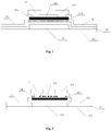
- the present embodiment provides a thin film transistor, comprising a base 101, a gate 102, a gate insulation layer 103, a semiconductor active region 105, and a source and drain 107 connected with the semiconductor active region 105, and the thin film transistor further comprises a surface charge transfer layer 104 in contact with the semiconductor active region 105, wherein, the surface charge transfer layer 104 is located above or below the semiconductor active region 105, and is used for causing the semiconductor active region 105 to generate a large number of holes therein without changing the lattice structure of the semiconductor active region 105.
- charge transfer occurs between the semiconductor active region 105 and the surface charge transfer layer 104, thus a large number of holes is generated near the interface where the semiconductor active region 105 and the surface charge transfer layer 104 are in contact with each other, the semiconductor active region 105 is converted into a P-type semiconductor active region 105.
- Energy level difference between the lowest unoccupied molecular orbit (LOMO) of material of the surface charge transfer layer 104 and the top of valence band of material of the semiconductor active region 105 is between -1eV and 1eV (including the endpoint values).
- the thin film transistor of the present embodiment by causing charge transfer to occur between the semiconductor active region 105 and the surface charge transfer layer 104 in contact with the semiconductor active region 105, a large number of holes is generated in the semiconductor active region 105 so that the semiconductor active region 105 is converted into a doped semiconductor active region 105 without changing the conductive lattices of the semiconductor active region 105 itself, thus probability that the carriers are captured or scattered during moving in the lattices is greatly lowered, thereby the lifetime of the carriers is longer and the mobility of the carriers is higher, which will facilitate improving of performance of the thin film transistor.
- the thin film transistor is a bottom gate type thin film transistor, which preferably comprises: the gate 102, the gate insulation layer 103 covering the gate 102, the surface charge transfer layer 104 provided above the gate insulation layer 103, the semiconductor active region 105 provided above the surface charge transfer layer 104, and the source and drain 107, which are sequentially provided on the base 101, wherein the source and drain 107 are connected with the semiconductor active region 105 through contact holes penetrating through an etch stopper 106 above the semiconductor active region 105.
- the thin film transistor may preferably comprise: the gate 102, the gate insulation layer 103 covering the gate 102, the semiconductor active region 105 provided above the gate insulation layer 103, the surface charge transfer layer 104 provided above the semiconductor active region 105, and the source and drain 107, which are sequentially provided on the base 101, wherein the source and drain 107 are connected with the semiconductor active region 105 through contact holes penetrating through the etch stopper 106 and the surface charge transfer layer 104 above the semiconductor active region 105.
- the thin film transistor is preferably a top gate type thin film transistor, which preferably comprises: the surface charge transfer layer 104, the semiconductor active region 105, and the gate 102 provided above the semiconductor active region 105, which are sequentially provided on the base 101, wherein the gate 102 and the semiconductor active region 105 are separated from each other by the gate insulation layer 103, the etch stopper 106 is provided above the gate 102, the source and drain 107 are provided above the etch stopper 106, and the source and drain 107 are connected with the semiconductor active region 105 through contact holes penetrating through the etch stopper 106 and the gate insulation layer 103.
- the thin film transistor may preferably comprise: the semiconductor active region 105, the surface charge transfer layer 104, and the gate 102 provided above the surface charge transfer layer 104, which are sequentially provided on the base 101, wherein the gate 102 and the surface charge transfer layer 104 are separated from each other by the gate insulation layer 103, the etch stopper 106 is provided above the gate 102, and the source and drain 107 are provided above the etch stopper 106, the source and drain 107 are connected with the semiconductor active region 105 through contact holes penetrating through the etch stopper 106, the gate insulation layer 103 and the surface charge transfer layer 104.
- the material of the surface charge transfer layer 104 in the present embodiment is molybdenum trioxide, and the material of the semiconductor active region 105 is zinc oxide.
- Zinc oxide is used as the material of the semiconductor active region 105 so that the resultant thin film transistor has a higher mobility, thus size of the thin film transistor is reduced. A better effect is achieved by the above combination of molybdenum trioxide and zinc oxide.
- Fig.5 shows a schematic diagram illustrating energy bands of zinc oxide and molybdenum trioxide
- Fig.6 shows a schematic diagram illustrating energy band structures of zinc oxide and molybdenum trioxide before they are in contact with each other
- Fig.7 shows a schematic diagram illustrating energy band structures of zinc oxide and molybdenum trioxide after they are in contact with each other.
- the energy level of the top of valence band of zinc oxide is -7.39ev
- the energy level of the lowest unoccupied molecular orbit of molybdenum trioxide is -6.7ev.
- the intrinsic lattices of zinc oxide are maintained and are not changed, thus the probability that the carriers are captured and scattered during moving in the lattices is greatly lowered, thereby the lifetime of the carriers is longer, the mobility of the carriers is higher, which facilitate improving of performance of the thin film transistor.
- the present embodiment provides a manufacturing method of the thin film transistor in the first embodiment.
- the thin film transistor may be of top gate type or bottom gate type.
- An example in which the thin film transistor is of bottom gate type and the surface charge transfer layer 104 is provided below the semiconductor active region 105 will be described specifically below.
- the manufacturing method comprises following steps.
- the gate 102 may be a monolayer or multilayer composite stack layer formed of one or more of molybdenum (Mo), alloy of molybdenum and niobium (MoNb), aluminum (Al), alloy of aluminum and neodymium (AlNd), titanium (Ti) and copper (Cu), and preferably, is a monolayer or multilayer composite stack layer formed of Mo, Al or alloy containing Mo, Al, and the thickness thereof is between 100nm and 500nm.
- Mo molybdenum
- MoNb molybdenum
- Al aluminum
- AlNd aluminum and neodymium
- Ti titanium
- Cu copper
- the gate insulation layer 103 may be a multilayer composite film formed of one or two of silicon oxide (SiOx), silicon nitride (SiNx), hafnium oxide (HfOx), silicon oxynitride (SiON), aluminum oxide (AlOx), etc., the thickness thereof is between 100nm and 600nm, and the thickness may be adjusted in accordance with actual conditions.
- Step 3 sequentially depositing a transition insulation material layer, a semiconductor material layer above the gate insulation layer 103, and simultaneously forming a pattern of the surface charge transfer layer 104 and a pattern of the semiconductor active region 105 by performing exposure, development, etching, stripping, etc once.
- the surface charge transfer layer 104 and the semiconductor active region 105 are formed by a single patterning process, so that the cost is reduced and the productivity is improved.
- the pattern of the surface charge transfer layer 104 and the pattern of the semiconductor active region 105 may be formed by two steps.
- the material of the surface charge transfer layer 104 is molybdenum trioxide, and the material of the semiconductor active region 105 is zinc oxide.
- Step 4 forming the etch stopper (ESL) 106 above the semiconductor active region 105 by sputtering, exposure, development, etching, stripping, etc.
- the etch stopper 106 may be a multilayer film formed of two or three of silicon oxide (SiOx), silicon nitride (SiNx), hafnium oxide (HfOx), silicon oxynitride (SiON), aluminum oxide (AlOx), etc.
- the source and drain 107 may be a monolayer or multilayer composite stack layer formed of one or more of molybdenum (Mo), alloy of molybdenum and niobium (MoNb), aluminum (Al), alloy of aluminum and neodymium (AlNd), titanium (Ti) and copper (Cu), and preferably, is a monolayer or multilayer composite stack layer formed of Mo, Al or alloy containing Mo, Al.
- Mo molybdenum
- MoNb molybdenum
- Al aluminum
- AlNd aluminum and neodymium
- Ti titanium
- Cu copper
- the passivation layer may be formed of one or several of silicon oxide (SiOx), silicon nitride (SiNx), hafnium oxide (HfOx), silicon oxynitride (SiON), aluminum oxide (AlOx) and organic material.
- a bottom gate type thin film transistor is manufactured.
- this thin film transistor by causing charge transfer to occur between the semiconductor active region 105 and the surface charge transfer layer 104, a large number of holes is generated in the semiconductor active region 105 so that the semiconductor active region 105 is converted into a doped semiconductor active region 105 without changing the conductive lattices of the semiconductor active region 105 itself, thus probability that the carriers are captured or scattered during moving in the lattices is greatly lowered, thereby the lifetime of the carriers is longer and the mobility of the carriers is higher, which will facilitate improving of performance of the thin film transistor.
- the manufacturing method of the bottom gate type thin film transistor in which the semiconductor active region 105 is provided below the surface charge transfer layer 104 is similar to the above method, the difference is in that: a transition insulation material layer and a semiconductor material layer are sequentially deposited on the base formed with the gate insulation layer 103.
- the surface charge transfer layer 104 and the semiconductor active region 105 of the top gate type thin film transistor are formed by a method similar to the method in the present embodiment, the difference is in that: the semiconductor active region 105 and the surface charge transfer layer 104 of the top gate type thin film transistor are formed before the gate insulation layer 103 is formed, and other steps are substantially the same and will not be repeated here.
- the present embodiment provides an array substrate comprising the thin film transistor of the first embodiment, wherein the source 107 of the thin film transistor is connected with a data signal line 108, and the drain 107 of the thin film transistor is connected with a pixel electrode 109.
- the array substrate further comprises a mesh-shaped common electrode 111, the pixel electrode 109 and the common electrode 111 are separated from each other by a passivation layer 110, a first electrode of a storage capacitor is integrated with the pixel electrode 109 as a whole, and a second electrode of the storage capacitor is integrated with the common electrode 111 as a whole.
- ADS ADvanced super dimension switch
- the pixel electrode 109 may be a mesh-shaped electrode
- the common electrode 111 is a plate-shaped electrode
- the data signal line 108 and the source and drain 107 are formed synchronously. In this case, the cost is reduced, and the productivity is improved.
- material of the pixel electrode 109 and the common electrode 111 is indium tin oxide (ITO) or graphene, or may be any other transparent conductive material.
- the present invention is not limited to the array substrate in the liquid crystal display apparatus of ADS mode, and even is not limited to the array substrate in the liquid crystal display device.
- the present invention may be applied to the array substrate in the liquid crystal display device of IPS (in-plane switch) mode, the array substrate in the OLED (organic light emitting diode) display device, and the like.
- the present embodiment provides a manufacturing method of the array substrate in the third embodiment, wherein the manufacturing of the thin film transistor is the same as that in the second embodiment, while forming the thin film transistor, the manufacturing method further comprises following steps.
- Step 7 forming a pattern of the pixel electrode 109 (i.e., the first electrode of the storage capacitor) above the contact holes for connecting the drain 107 and the semiconductor active region 105 of the thin film transistor by a patterning process, wherein the material of the pixel electrode 109 (the first electrode of the storage capacitor) is a conductive material of indium tin oxide, graphene, or the like.
- Step 8 forming the source and drain 107 of the thin film transistor on the base 101 subjected to the above step, and meanwhile, forming the data signal line 108 connected with the source 107.
- the above two steps may be performed by a single patterning process. Specifically, a pixel electrode material layer is deposited above the contact holes for connecting the drain 107 and the semiconductor active region 105 of the thin film transistor, then a source and drain metal layer is deposited above the contact holes for connecting the source 107 and the semiconductor active region 105 of the thin film transistor and above the pixel electrode material layer, a pattern including the source 107, the drain 107, the data signal line 108 connected with the source 107, and the pixel electrode 109 connected with the drain 107 are formed by exposure, development, etching, stripping, etc. Since the source and drain 107, the data signal line 108 and the pixel electrode 109 are formed by a single patterning process, the productivity is improved and the cost is reduced.
- the passivation layer 110 is formed on the base 101 subjected to the above steps, and a pattern of the common electrode 111 (i.e., the second electrode of the storage capacitor) is formed by a patterning process, wherein the material of the common electrode 111 (the second electrode of the storage capacitor) is a conductive material of indium tin oxide, graphene, or the like.
- the pixel electrode 109 is first prepared, and then the common electrode 111 is manufactured.
- the common electrode 111 is first prepared and then the pixel electrode 109 is manufactured, which is also within the scope of the present invention.
- the present embodiment provides a display apparatus comprising the array substrate of the third embodiment.
- the display apparatus may be any product or member with display function, such as phone, tablet computer, TV, monitor, notebook computer, digital photo frame, and navigator.
- the display apparatus of the present embodiment comprises the array substrate of the third embodiment, thus the performance of the thin film transistor therein is significantly improved, and the performance of the display apparatus is also improved.
- the display apparatus of the present embodiment may further comprise other conventional structures such as a power source, a display drive unit and so on.
Landscapes
- Thin Film Transistor (AREA)
Claims (9)
- Dünnfilmtransistor, umfassend: ein Gate (102), eine Gate-Isolierschicht (103), einen aktiven Halbleiterbereich (105) und eine Source (107) und einen Drain (107), die mit dem aktiven Halbleiterbereich (105) verbunden sind, wobei der Dünnfilmtransistor ferner eine Oberflächenladungsübertragungsschicht (104) umfasst, die mit dem aktiven Halbleiterbereich (105) in Berührung steht, wobei die Oberflächenladungsübertragungsschicht (104) oberhalb oder unterhalb des aktiven Halbleiterbereichs (105) angeordnet ist, und verwendet wird, um zu bewirken, dass der aktive Halbleiterbereich (105) darin Löcher erzeugt, ohne die Gitterstruktur des aktiven Halbleiterbereichs (105) zu verändern;
wobei die Energiepegeldifferenz zwischen der niedrigsten unbesetzten molekularen Umlaufbahn von Material der Oberflächenladungsübertragungsschicht (104) und der Oberseite eines Valenzbands von Material des aktiven Halbleiterbereichs (105) größer oder gleich -1 eV und kleiner oder gleich 1 eV ist, und
wobei das Material des aktiven Halbleiterbereichs (105) Zinkoxid ist und das Material der Oberflächenladungsübertragungsschicht (104) Molybdäntrioxid ist. - Dünnfilmtransistor nach Anspruch 1, wobei das Gate (102) auf einer Basis (101) vorgesehen ist, die Gate-Isolierschicht (103) das Gate (102) bedeckt, die Oberflächenladungsübertragungsschicht (104) oberhalb der Gate-Isolierschicht (103) vorgesehen ist und der aktive Halbleiterbereich (105) oberhalb der Oberflächenladungsübertragungsschicht (104) vorgesehen ist.
- Dünnfilmtransistor nach Anspruch 1, wobei das Gate (102) auf einer Basis (101) vorgesehen ist, die Gate-Isolierschicht (103) das Gate (102) bedeckt, der aktive Halbleiterbereich (105) oberhalb der Gate-Isolierschicht (103) vorgesehen ist und die Oberflächenladungsübertragungsschicht (104) oberhalb des aktiven Halbleiterbereichs (105) vorgesehen ist.
- Dünnfilmtransistor nach Anspruch 1, wobei die Oberflächenladungsübertragungsschicht (104) und der aktive Halbleiterbereich (105) nacheinander auf einer Basis (101) vorgesehen sind, das Gate (102) oberhalb des aktiven Halbleiterbereichs (105) vorgesehen ist und das Gate (102) und der aktive Halbleiterbereich (105) durch die Gate-Isolierschicht (103) voneinander getrennt sind.
- Dünnfilmtransistor nach Anspruch 1, wobei der aktive Halbleiterbereich (105) und die Oberflächenladungsübertragungsschicht (104) nacheinander auf einer Basis (101) vorgesehen sind, das Gate (102) oberhalb der Oberflächenladungsübertragungsschicht (104) vorgesehen ist und das Gate (102) und die Oberflächenladungsübertragungsschicht (104) durch die Gate-Isolierschicht (103) voneinander getrennt sind.
- Herstellungsverfahren des Dünnfilmtransistors nach einem der Ansprüche 1 bis 5 mit dem Schritt: Bilden eines Musters der Oberflächenladungsübertragungsschicht- (104) oberhalb oder unterhalb eines Musters des aktiven Halbleiterbereichs (105).
- Herstellungsverfahren nach Anspruch 6, wobei das Muster der Oberflächenladungsübertragungsschicht (104) und das Muster des aktiven Halbleiterbereichs (105) durch einen einzigen Strukturierungsprozess gebildet werden.
- Arraysubstrat, den Dünnfilmtransistor nach einem der Ansprüche 1 bis 5 umfassend.
- Anzeigevorrichtung, das Arraysubstrat nach Anspruch 8 umfassend.
Applications Claiming Priority (2)
| Application Number | Priority Date | Filing Date | Title |
|---|---|---|---|
| CN201310500440.9A CN103531639B (zh) | 2013-10-22 | 2013-10-22 | 薄膜晶体管及其制备方法、阵列基板、显示装置 |
| PCT/CN2014/082241 WO2015058562A1 (zh) | 2013-10-22 | 2014-07-15 | 薄膜晶体管及其制备方法、阵列基板、显示装置 |
Publications (3)
| Publication Number | Publication Date |
|---|---|
| EP2908348A1 EP2908348A1 (de) | 2015-08-19 |
| EP2908348A4 EP2908348A4 (de) | 2016-06-22 |
| EP2908348B1 true EP2908348B1 (de) | 2019-12-04 |
Family
ID=49933494
Family Applications (1)
| Application Number | Title | Priority Date | Filing Date |
|---|---|---|---|
| EP14856040.2A Active EP2908348B1 (de) | 2013-10-22 | 2014-07-15 | Dünnfilmtransistor und dessen herstellungsverfahren, arraysubstrat und anzeigevorrichtung |
Country Status (4)
| Country | Link |
|---|---|
| US (1) | US9484468B2 (de) |
| EP (1) | EP2908348B1 (de) |
| CN (1) | CN103531639B (de) |
| WO (1) | WO2015058562A1 (de) |
Families Citing this family (8)
| Publication number | Priority date | Publication date | Assignee | Title |
|---|---|---|---|---|
| CN103531639B (zh) | 2013-10-22 | 2016-09-07 | 合肥京东方光电科技有限公司 | 薄膜晶体管及其制备方法、阵列基板、显示装置 |
| CN104952932A (zh) * | 2015-05-29 | 2015-09-30 | 合肥鑫晟光电科技有限公司 | 薄膜晶体管、阵列基板及其制作方法、显示装置 |
| CN105261654B (zh) | 2015-11-05 | 2018-12-28 | 京东方科技集团股份有限公司 | 低温多晶硅薄膜晶体管及制作方法、阵列基板、显示面板 |
| CN105892747A (zh) * | 2016-04-06 | 2016-08-24 | 深圳市华星光电技术有限公司 | 触摸显示面板、其制备方法以及触摸显示器 |
| WO2019112601A1 (en) * | 2017-12-08 | 2019-06-13 | Hewlett-Packard Development Company, L.P. | Dual-sided displays |
| JP2022014108A (ja) * | 2020-07-06 | 2022-01-19 | シャープ株式会社 | アクティブマトリクス基板およびその製造方法 |
| CN114447118B (zh) * | 2022-01-17 | 2026-02-06 | Tcl华星光电技术有限公司 | 晶体管及其制备方法、显示面板 |
| WO2025214967A1 (en) * | 2024-04-08 | 2025-10-16 | Qurv Technologies Sl | Photodetector, image sensor and photodetection method |
Family Cites Families (12)
| Publication number | Priority date | Publication date | Assignee | Title |
|---|---|---|---|---|
| FR2537781B1 (fr) | 1982-12-14 | 1986-05-30 | Thomson Csf | Transistor a effet de champ, fonctionnant en regime d'accumulation par gaz d'electrons |
| JP2005166729A (ja) | 2003-11-28 | 2005-06-23 | Seiko Epson Corp | 半導体装置及びその製造方法 |
| CN1309032C (zh) * | 2004-02-25 | 2007-04-04 | 友达光电股份有限公司 | 薄膜晶体管的结构和制造方法 |
| KR101345376B1 (ko) * | 2007-05-29 | 2013-12-24 | 삼성전자주식회사 | ZnO 계 박막 트랜지스터 및 그 제조방법 |
| JP5311955B2 (ja) * | 2007-11-01 | 2013-10-09 | 株式会社半導体エネルギー研究所 | 表示装置の作製方法 |
| KR101508806B1 (ko) | 2008-04-28 | 2015-04-06 | 다이니폰 인사츠 가부시키가이샤 | 정공 주입 수송층을 갖는 디바이스, 및 그 제조 방법, 및 정공 주입 수송층 형성용 잉크 |
| KR100963026B1 (ko) | 2008-06-30 | 2010-06-10 | 삼성모바일디스플레이주식회사 | 박막 트랜지스터, 그의 제조 방법 및 박막 트랜지스터를구비하는 평판 표시 장치 |
| KR100963027B1 (ko) * | 2008-06-30 | 2010-06-10 | 삼성모바일디스플레이주식회사 | 박막 트랜지스터, 그의 제조 방법 및 박막 트랜지스터를구비하는 평판 표시 장치 |
| US8704216B2 (en) | 2009-02-27 | 2014-04-22 | Semiconductor Energy Laboratory Co., Ltd. | Semiconductor device and manufacturing method thereof |
| US8975509B2 (en) | 2010-06-07 | 2015-03-10 | The Governing Council Of The University Of Toronto | Photovoltaic devices with multiple junctions separated by a graded recombination layer |
| KR20110139394A (ko) * | 2010-06-23 | 2011-12-29 | 주성엔지니어링(주) | 박막 트랜지스터 및 그 제조 방법 |
| CN103531639B (zh) | 2013-10-22 | 2016-09-07 | 合肥京东方光电科技有限公司 | 薄膜晶体管及其制备方法、阵列基板、显示装置 |
-
2013
- 2013-10-22 CN CN201310500440.9A patent/CN103531639B/zh not_active Expired - Fee Related
-
2014
- 2014-07-15 US US14/429,940 patent/US9484468B2/en active Active
- 2014-07-15 EP EP14856040.2A patent/EP2908348B1/de active Active
- 2014-07-15 WO PCT/CN2014/082241 patent/WO2015058562A1/zh not_active Ceased
Non-Patent Citations (1)
| Title |
|---|
| MIKHAILOVA M P ET AL: "TOPICAL REVIEW; Interface-induced optical and transport phenomena in type II broken-gap single heterojunctions; Topical Review", SEMICONDUCTOR SCIENCE AND TECHNOLOGY, IOP PUBLISHING LTD, GB, vol. 19, no. 10, 1 October 2004 (2004-10-01), pages R109 - R128, XP020032386, ISSN: 0268-1242, DOI: 10.1088/0268-1242/19/10/R03 * |
Also Published As
| Publication number | Publication date |
|---|---|
| WO2015058562A1 (zh) | 2015-04-30 |
| CN103531639B (zh) | 2016-09-07 |
| US9484468B2 (en) | 2016-11-01 |
| CN103531639A (zh) | 2014-01-22 |
| EP2908348A4 (de) | 2016-06-22 |
| US20160027931A1 (en) | 2016-01-28 |
| EP2908348A1 (de) | 2015-08-19 |
Similar Documents
| Publication | Publication Date | Title |
|---|---|---|
| US9484468B2 (en) | Thin film transistor and manufacturing method thereof, array substrate, and display apparatus | |
| US9748280B2 (en) | Thin film transistor and method of fabricating the same, array substrate and method of fabricating the same, and display device | |
| EP3121840B1 (de) | Dünnschichttransistor und herstellungsverfahren dafür, arraysubstrat und anzeigetafel | |
| US9818775B2 (en) | Array substrate, manufacturing method thereof, display device, thin-film transistor (TFT) and manufacturing method thereof | |
| US9614098B2 (en) | Thin film transistor and manufacturing method thereof, array substrate and display device | |
| US9312146B2 (en) | Manufacturing method of a thin film transistor | |
| US10658446B2 (en) | Method for manufacturing OLED backplane comprising active layer formed of first, second, and third oxide semiconductor layers | |
| US9202896B2 (en) | TFT, method of manufacturing the TFT, and method of manufacturing organic light emitting display device including the TFT | |
| US10083988B2 (en) | Complementary thin film transistor and manufacturing method thereof, array substrate, display apparatus | |
| CN109119440B (zh) | Oled背板及其制作方法 | |
| EP3089217B1 (de) | Dünnschichttransistor, herstellungsverfahren dafür, arraysubstrat und anzeigevorrichtung | |
| US11925064B2 (en) | Manufacturing method of display substrate and display device | |
| US20160343739A1 (en) | Thin film transistor, method of manufacturing thin film transistor, array substrate and display device | |
| CN103354218A (zh) | 阵列基板及其制作方法和显示装置 | |
| US9171941B2 (en) | Fabricating method of thin film transistor, fabricating method of array substrate and display device | |
| CN104091810A (zh) | 阵列基板及其制作方法、显示装置 | |
| CN107464820A (zh) | Esl型tft基板及其制作方法 | |
| US9196636B2 (en) | TFT and manufacturing method thereof, array substrate and display device | |
| US20240072063A1 (en) | Drive substrate, manufacturing method thereof and display panel | |
| CN105097829A (zh) | 阵列基板及其制备方法 | |
| US20140027760A1 (en) | Semiconductor device and manufacturing method thereof | |
| WO2022116313A1 (zh) | 一种阵列基板、显示面板及其制备方法 | |
| US20240222445A1 (en) | Thin film transistor, manufacturing method thereof, and array substrate | |
| CN215771156U (zh) | 显示面板及显示装置 | |
| US20190131143A1 (en) | Thin-Film Transistor And Method Of Manufacturing The Same, Array Substrate, And Display Apparatus |
Legal Events
| Date | Code | Title | Description |
|---|---|---|---|
| PUAI | Public reference made under article 153(3) epc to a published international application that has entered the european phase |
Free format text: ORIGINAL CODE: 0009012 |
|
| 17P | Request for examination filed |
Effective date: 20150515 |
|
| AK | Designated contracting states |
Kind code of ref document: A1 Designated state(s): AL AT BE BG CH CY CZ DE DK EE ES FI FR GB GR HR HU IE IS IT LI LT LU LV MC MK MT NL NO PL PT RO RS SE SI SK SM TR |
|
| AX | Request for extension of the european patent |
Extension state: BA ME |
|
| R17P | Request for examination filed (corrected) |
Effective date: 20150515 |
|
| RA4 | Supplementary search report drawn up and despatched (corrected) |
Effective date: 20160524 |
|
| RIC1 | Information provided on ipc code assigned before grant |
Ipc: H01L 29/786 20060101AFI20160518BHEP Ipc: H01L 29/24 20060101ALI20160518BHEP Ipc: H01L 27/12 20060101ALI20160518BHEP |
|
| DAX | Request for extension of the european patent (deleted) | ||
| STAA | Information on the status of an ep patent application or granted ep patent |
Free format text: STATUS: EXAMINATION IS IN PROGRESS |
|
| 17Q | First examination report despatched |
Effective date: 20180606 |
|
| RIC1 | Information provided on ipc code assigned before grant |
Ipc: H01L 29/24 20060101ALI20190412BHEP Ipc: H01L 29/786 20060101AFI20190412BHEP |
|
| GRAP | Despatch of communication of intention to grant a patent |
Free format text: ORIGINAL CODE: EPIDOSNIGR1 |
|
| STAA | Information on the status of an ep patent application or granted ep patent |
Free format text: STATUS: GRANT OF PATENT IS INTENDED |
|
| INTG | Intention to grant announced |
Effective date: 20190618 |
|
| GRAS | Grant fee paid |
Free format text: ORIGINAL CODE: EPIDOSNIGR3 |
|
| GRAA | (expected) grant |
Free format text: ORIGINAL CODE: 0009210 |
|
| STAA | Information on the status of an ep patent application or granted ep patent |
Free format text: STATUS: THE PATENT HAS BEEN GRANTED |
|
| AK | Designated contracting states |
Kind code of ref document: B1 Designated state(s): AL AT BE BG CH CY CZ DE DK EE ES FI FR GB GR HR HU IE IS IT LI LT LU LV MC MK MT NL NO PL PT RO RS SE SI SK SM TR |
|
| RAP1 | Party data changed (applicant data changed or rights of an application transferred) |
Owner name: HEFEI BOE OPTOELECTRONICS TECHNOLOGY CO., LTD. Owner name: BOE TECHNOLOGY GROUP CO., LTD. |
|
| REG | Reference to a national code |
Ref country code: GB Ref legal event code: FG4D |
|
| REG | Reference to a national code |
Ref country code: CH Ref legal event code: EP |
|
| REG | Reference to a national code |
Ref country code: AT Ref legal event code: REF Ref document number: 1210486 Country of ref document: AT Kind code of ref document: T Effective date: 20191215 |
|
| REG | Reference to a national code |
Ref country code: DE Ref legal event code: R096 Ref document number: 602014058020 Country of ref document: DE |
|
| REG | Reference to a national code |
Ref country code: IE Ref legal event code: FG4D |
|
| REG | Reference to a national code |
Ref country code: NL Ref legal event code: MP Effective date: 20191204 |
|
| REG | Reference to a national code |
Ref country code: LT Ref legal event code: MG4D |
|
| PG25 | Lapsed in a contracting state [announced via postgrant information from national office to epo] |
Ref country code: FI Free format text: LAPSE BECAUSE OF FAILURE TO SUBMIT A TRANSLATION OF THE DESCRIPTION OR TO PAY THE FEE WITHIN THE PRESCRIBED TIME-LIMIT Effective date: 20191204 Ref country code: GR Free format text: LAPSE BECAUSE OF FAILURE TO SUBMIT A TRANSLATION OF THE DESCRIPTION OR TO PAY THE FEE WITHIN THE PRESCRIBED TIME-LIMIT Effective date: 20200305 Ref country code: BG Free format text: LAPSE BECAUSE OF FAILURE TO SUBMIT A TRANSLATION OF THE DESCRIPTION OR TO PAY THE FEE WITHIN THE PRESCRIBED TIME-LIMIT Effective date: 20200304 Ref country code: NO Free format text: LAPSE BECAUSE OF FAILURE TO SUBMIT A TRANSLATION OF THE DESCRIPTION OR TO PAY THE FEE WITHIN THE PRESCRIBED TIME-LIMIT Effective date: 20200304 Ref country code: LV Free format text: LAPSE BECAUSE OF FAILURE TO SUBMIT A TRANSLATION OF THE DESCRIPTION OR TO PAY THE FEE WITHIN THE PRESCRIBED TIME-LIMIT Effective date: 20191204 Ref country code: SE Free format text: LAPSE BECAUSE OF FAILURE TO SUBMIT A TRANSLATION OF THE DESCRIPTION OR TO PAY THE FEE WITHIN THE PRESCRIBED TIME-LIMIT Effective date: 20191204 Ref country code: LT Free format text: LAPSE BECAUSE OF FAILURE TO SUBMIT A TRANSLATION OF THE DESCRIPTION OR TO PAY THE FEE WITHIN THE PRESCRIBED TIME-LIMIT Effective date: 20191204 |
|
| PG25 | Lapsed in a contracting state [announced via postgrant information from national office to epo] |
Ref country code: RS Free format text: LAPSE BECAUSE OF FAILURE TO SUBMIT A TRANSLATION OF THE DESCRIPTION OR TO PAY THE FEE WITHIN THE PRESCRIBED TIME-LIMIT Effective date: 20191204 Ref country code: HR Free format text: LAPSE BECAUSE OF FAILURE TO SUBMIT A TRANSLATION OF THE DESCRIPTION OR TO PAY THE FEE WITHIN THE PRESCRIBED TIME-LIMIT Effective date: 20191204 |
|
| PG25 | Lapsed in a contracting state [announced via postgrant information from national office to epo] |
Ref country code: AL Free format text: LAPSE BECAUSE OF FAILURE TO SUBMIT A TRANSLATION OF THE DESCRIPTION OR TO PAY THE FEE WITHIN THE PRESCRIBED TIME-LIMIT Effective date: 20191204 |
|
| PG25 | Lapsed in a contracting state [announced via postgrant information from national office to epo] |
Ref country code: NL Free format text: LAPSE BECAUSE OF FAILURE TO SUBMIT A TRANSLATION OF THE DESCRIPTION OR TO PAY THE FEE WITHIN THE PRESCRIBED TIME-LIMIT Effective date: 20191204 Ref country code: PT Free format text: LAPSE BECAUSE OF FAILURE TO SUBMIT A TRANSLATION OF THE DESCRIPTION OR TO PAY THE FEE WITHIN THE PRESCRIBED TIME-LIMIT Effective date: 20200429 Ref country code: EE Free format text: LAPSE BECAUSE OF FAILURE TO SUBMIT A TRANSLATION OF THE DESCRIPTION OR TO PAY THE FEE WITHIN THE PRESCRIBED TIME-LIMIT Effective date: 20191204 Ref country code: CZ Free format text: LAPSE BECAUSE OF FAILURE TO SUBMIT A TRANSLATION OF THE DESCRIPTION OR TO PAY THE FEE WITHIN THE PRESCRIBED TIME-LIMIT Effective date: 20191204 Ref country code: RO Free format text: LAPSE BECAUSE OF FAILURE TO SUBMIT A TRANSLATION OF THE DESCRIPTION OR TO PAY THE FEE WITHIN THE PRESCRIBED TIME-LIMIT Effective date: 20191204 Ref country code: ES Free format text: LAPSE BECAUSE OF FAILURE TO SUBMIT A TRANSLATION OF THE DESCRIPTION OR TO PAY THE FEE WITHIN THE PRESCRIBED TIME-LIMIT Effective date: 20191204 |
|
| PG25 | Lapsed in a contracting state [announced via postgrant information from national office to epo] |
Ref country code: SM Free format text: LAPSE BECAUSE OF FAILURE TO SUBMIT A TRANSLATION OF THE DESCRIPTION OR TO PAY THE FEE WITHIN THE PRESCRIBED TIME-LIMIT Effective date: 20191204 Ref country code: IS Free format text: LAPSE BECAUSE OF FAILURE TO SUBMIT A TRANSLATION OF THE DESCRIPTION OR TO PAY THE FEE WITHIN THE PRESCRIBED TIME-LIMIT Effective date: 20200404 Ref country code: SK Free format text: LAPSE BECAUSE OF FAILURE TO SUBMIT A TRANSLATION OF THE DESCRIPTION OR TO PAY THE FEE WITHIN THE PRESCRIBED TIME-LIMIT Effective date: 20191204 |
|
| REG | Reference to a national code |
Ref country code: DE Ref legal event code: R097 Ref document number: 602014058020 Country of ref document: DE |
|
| REG | Reference to a national code |
Ref country code: AT Ref legal event code: MK05 Ref document number: 1210486 Country of ref document: AT Kind code of ref document: T Effective date: 20191204 |
|
| PLBE | No opposition filed within time limit |
Free format text: ORIGINAL CODE: 0009261 |
|
| STAA | Information on the status of an ep patent application or granted ep patent |
Free format text: STATUS: NO OPPOSITION FILED WITHIN TIME LIMIT |
|
| PG25 | Lapsed in a contracting state [announced via postgrant information from national office to epo] |
Ref country code: DK Free format text: LAPSE BECAUSE OF FAILURE TO SUBMIT A TRANSLATION OF THE DESCRIPTION OR TO PAY THE FEE WITHIN THE PRESCRIBED TIME-LIMIT Effective date: 20191204 |
|
| 26N | No opposition filed |
Effective date: 20200907 |
|
| PG25 | Lapsed in a contracting state [announced via postgrant information from national office to epo] |
Ref country code: AT Free format text: LAPSE BECAUSE OF FAILURE TO SUBMIT A TRANSLATION OF THE DESCRIPTION OR TO PAY THE FEE WITHIN THE PRESCRIBED TIME-LIMIT Effective date: 20191204 Ref country code: PL Free format text: LAPSE BECAUSE OF FAILURE TO SUBMIT A TRANSLATION OF THE DESCRIPTION OR TO PAY THE FEE WITHIN THE PRESCRIBED TIME-LIMIT Effective date: 20191204 Ref country code: SI Free format text: LAPSE BECAUSE OF FAILURE TO SUBMIT A TRANSLATION OF THE DESCRIPTION OR TO PAY THE FEE WITHIN THE PRESCRIBED TIME-LIMIT Effective date: 20191204 |
|
| PG25 | Lapsed in a contracting state [announced via postgrant information from national office to epo] |
Ref country code: IT Free format text: LAPSE BECAUSE OF FAILURE TO SUBMIT A TRANSLATION OF THE DESCRIPTION OR TO PAY THE FEE WITHIN THE PRESCRIBED TIME-LIMIT Effective date: 20191204 |
|
| PG25 | Lapsed in a contracting state [announced via postgrant information from national office to epo] |
Ref country code: MC Free format text: LAPSE BECAUSE OF FAILURE TO SUBMIT A TRANSLATION OF THE DESCRIPTION OR TO PAY THE FEE WITHIN THE PRESCRIBED TIME-LIMIT Effective date: 20191204 |
|
| REG | Reference to a national code |
Ref country code: CH Ref legal event code: PL |
|
| REG | Reference to a national code |
Ref country code: BE Ref legal event code: MM Effective date: 20200731 |
|
| PG25 | Lapsed in a contracting state [announced via postgrant information from national office to epo] |
Ref country code: LI Free format text: LAPSE BECAUSE OF NON-PAYMENT OF DUE FEES Effective date: 20200731 Ref country code: LU Free format text: LAPSE BECAUSE OF NON-PAYMENT OF DUE FEES Effective date: 20200715 Ref country code: CH Free format text: LAPSE BECAUSE OF NON-PAYMENT OF DUE FEES Effective date: 20200731 |
|
| PG25 | Lapsed in a contracting state [announced via postgrant information from national office to epo] |
Ref country code: BE Free format text: LAPSE BECAUSE OF NON-PAYMENT OF DUE FEES Effective date: 20200731 |
|
| PG25 | Lapsed in a contracting state [announced via postgrant information from national office to epo] |
Ref country code: IE Free format text: LAPSE BECAUSE OF NON-PAYMENT OF DUE FEES Effective date: 20200715 |
|
| PG25 | Lapsed in a contracting state [announced via postgrant information from national office to epo] |
Ref country code: TR Free format text: LAPSE BECAUSE OF FAILURE TO SUBMIT A TRANSLATION OF THE DESCRIPTION OR TO PAY THE FEE WITHIN THE PRESCRIBED TIME-LIMIT Effective date: 20191204 Ref country code: MT Free format text: LAPSE BECAUSE OF FAILURE TO SUBMIT A TRANSLATION OF THE DESCRIPTION OR TO PAY THE FEE WITHIN THE PRESCRIBED TIME-LIMIT Effective date: 20191204 Ref country code: CY Free format text: LAPSE BECAUSE OF FAILURE TO SUBMIT A TRANSLATION OF THE DESCRIPTION OR TO PAY THE FEE WITHIN THE PRESCRIBED TIME-LIMIT Effective date: 20191204 |
|
| PG25 | Lapsed in a contracting state [announced via postgrant information from national office to epo] |
Ref country code: MK Free format text: LAPSE BECAUSE OF FAILURE TO SUBMIT A TRANSLATION OF THE DESCRIPTION OR TO PAY THE FEE WITHIN THE PRESCRIBED TIME-LIMIT Effective date: 20191204 |
|
| P01 | Opt-out of the competence of the unified patent court (upc) registered |
Effective date: 20230704 |
|
| PGFP | Annual fee paid to national office [announced via postgrant information from national office to epo] |
Ref country code: GB Payment date: 20240607 Year of fee payment: 11 |
|
| PGFP | Annual fee paid to national office [announced via postgrant information from national office to epo] |
Ref country code: FR Payment date: 20240604 Year of fee payment: 11 |
|
| PGFP | Annual fee paid to national office [announced via postgrant information from national office to epo] |
Ref country code: DE Payment date: 20240719 Year of fee payment: 11 |
|
| REG | Reference to a national code |
Ref country code: DE Ref legal event code: R079 Ref document number: 602014058020 Country of ref document: DE Free format text: PREVIOUS MAIN CLASS: H01L0029786000 Ipc: H10D0030670000 |
|
| REG | Reference to a national code |
Ref country code: DE Ref legal event code: R119 Ref document number: 602014058020 Country of ref document: DE |
|
| GBPC | Gb: european patent ceased through non-payment of renewal fee |
Effective date: 20250715 |
|
| PG25 | Lapsed in a contracting state [announced via postgrant information from national office to epo] |
Ref country code: GB Free format text: LAPSE BECAUSE OF NON-PAYMENT OF DUE FEES Effective date: 20250715 |
|
| PG25 | Lapsed in a contracting state [announced via postgrant information from national office to epo] |
Ref country code: DE Free format text: LAPSE BECAUSE OF NON-PAYMENT OF DUE FEES Effective date: 20260203 |
|
| PG25 | Lapsed in a contracting state [announced via postgrant information from national office to epo] |
Ref country code: FR Free format text: LAPSE BECAUSE OF NON-PAYMENT OF DUE FEES Effective date: 20250731 |