EP2903162A2 - Hybrides MDLL/PLL-Design mit gleichförmig verteilten Ausgangsphasen - Google Patents
Hybrides MDLL/PLL-Design mit gleichförmig verteilten Ausgangsphasen Download PDFInfo
- Publication number
- EP2903162A2 EP2903162A2 EP15152877.5A EP15152877A EP2903162A2 EP 2903162 A2 EP2903162 A2 EP 2903162A2 EP 15152877 A EP15152877 A EP 15152877A EP 2903162 A2 EP2903162 A2 EP 2903162A2
- Authority
- EP
- European Patent Office
- Prior art keywords
- delay
- output
- clock signal
- branch
- input
- Prior art date
- Legal status (The legal status is an assumption and is not a legal conclusion. Google has not performed a legal analysis and makes no representation as to the accuracy of the status listed.)
- Granted
Links
Images


Classifications
-
- H—ELECTRICITY
- H03—ELECTRONIC CIRCUITRY
- H03L—AUTOMATIC CONTROL, STARTING, SYNCHRONISATION OR STABILISATION OF GENERATORS OF ELECTRONIC OSCILLATIONS OR PULSES
- H03L7/00—Automatic control of frequency or phase; Synchronisation
- H03L7/06—Automatic control of frequency or phase; Synchronisation using a reference signal applied to a frequency- or phase-locked loop
- H03L7/08—Details of the phase-locked loop
- H03L7/081—Details of the phase-locked loop provided with an additional controlled phase shifter
- H03L7/0812—Details of the phase-locked loop provided with an additional controlled phase shifter and where no voltage or current controlled oscillator is used
-
- G—PHYSICS
- G09—EDUCATION; CRYPTOGRAPHY; DISPLAY; ADVERTISING; SEALS
- G09G—ARRANGEMENTS OR CIRCUITS FOR CONTROL OF INDICATING DEVICES USING STATIC MEANS TO PRESENT VARIABLE INFORMATION
- G09G3/00—Control arrangements or circuits, of interest only in connection with visual indicators other than cathode-ray tubes
- G09G3/20—Control arrangements or circuits, of interest only in connection with visual indicators other than cathode-ray tubes for presentation of an assembly of a number of characters, e.g. a page, by composing the assembly by combination of individual elements arranged in a matrix no fixed position being assigned to or needed to be assigned to the individual characters or partial characters
- G09G3/22—Control arrangements or circuits, of interest only in connection with visual indicators other than cathode-ray tubes for presentation of an assembly of a number of characters, e.g. a page, by composing the assembly by combination of individual elements arranged in a matrix no fixed position being assigned to or needed to be assigned to the individual characters or partial characters using controlled light sources
- G09G3/30—Control arrangements or circuits, of interest only in connection with visual indicators other than cathode-ray tubes for presentation of an assembly of a number of characters, e.g. a page, by composing the assembly by combination of individual elements arranged in a matrix no fixed position being assigned to or needed to be assigned to the individual characters or partial characters using controlled light sources using electroluminescent panels
- G09G3/32—Control arrangements or circuits, of interest only in connection with visual indicators other than cathode-ray tubes for presentation of an assembly of a number of characters, e.g. a page, by composing the assembly by combination of individual elements arranged in a matrix no fixed position being assigned to or needed to be assigned to the individual characters or partial characters using controlled light sources using electroluminescent panels semiconductive, e.g. using light-emitting diodes [LED]
- G09G3/3208—Control arrangements or circuits, of interest only in connection with visual indicators other than cathode-ray tubes for presentation of an assembly of a number of characters, e.g. a page, by composing the assembly by combination of individual elements arranged in a matrix no fixed position being assigned to or needed to be assigned to the individual characters or partial characters using controlled light sources using electroluminescent panels semiconductive, e.g. using light-emitting diodes [LED] organic, e.g. using organic light-emitting diodes [OLED]
-
- G—PHYSICS
- G09—EDUCATION; CRYPTOGRAPHY; DISPLAY; ADVERTISING; SEALS
- G09G—ARRANGEMENTS OR CIRCUITS FOR CONTROL OF INDICATING DEVICES USING STATIC MEANS TO PRESENT VARIABLE INFORMATION
- G09G3/00—Control arrangements or circuits, of interest only in connection with visual indicators other than cathode-ray tubes
- G09G3/20—Control arrangements or circuits, of interest only in connection with visual indicators other than cathode-ray tubes for presentation of an assembly of a number of characters, e.g. a page, by composing the assembly by combination of individual elements arranged in a matrix no fixed position being assigned to or needed to be assigned to the individual characters or partial characters
- G09G3/34—Control arrangements or circuits, of interest only in connection with visual indicators other than cathode-ray tubes for presentation of an assembly of a number of characters, e.g. a page, by composing the assembly by combination of individual elements arranged in a matrix no fixed position being assigned to or needed to be assigned to the individual characters or partial characters by control of light from an independent source
- G09G3/36—Control arrangements or circuits, of interest only in connection with visual indicators other than cathode-ray tubes for presentation of an assembly of a number of characters, e.g. a page, by composing the assembly by combination of individual elements arranged in a matrix no fixed position being assigned to or needed to be assigned to the individual characters or partial characters by control of light from an independent source using liquid crystals
-
- G—PHYSICS
- G09—EDUCATION; CRYPTOGRAPHY; DISPLAY; ADVERTISING; SEALS
- G09G—ARRANGEMENTS OR CIRCUITS FOR CONTROL OF INDICATING DEVICES USING STATIC MEANS TO PRESENT VARIABLE INFORMATION
- G09G5/00—Control arrangements or circuits for visual indicators common to cathode-ray tube indicators and other visual indicators
- G09G5/18—Timing circuits for raster scan displays
-
- H—ELECTRICITY
- H03—ELECTRONIC CIRCUITRY
- H03K—PULSE TECHNIQUE
- H03K5/00—Manipulating of pulses not covered by one of the other main groups of this subclass
- H03K5/13—Arrangements having a single output and transforming input signals into pulses delivered at desired time intervals
- H03K5/135—Arrangements having a single output and transforming input signals into pulses delivered at desired time intervals by the use of time reference signals, e.g. clock signals
-
- H—ELECTRICITY
- H03—ELECTRONIC CIRCUITRY
- H03L—AUTOMATIC CONTROL, STARTING, SYNCHRONISATION OR STABILISATION OF GENERATORS OF ELECTRONIC OSCILLATIONS OR PULSES
- H03L7/00—Automatic control of frequency or phase; Synchronisation
- H03L7/06—Automatic control of frequency or phase; Synchronisation using a reference signal applied to a frequency- or phase-locked loop
- H03L7/08—Details of the phase-locked loop
-
- H—ELECTRICITY
- H03—ELECTRONIC CIRCUITRY
- H03L—AUTOMATIC CONTROL, STARTING, SYNCHRONISATION OR STABILISATION OF GENERATORS OF ELECTRONIC OSCILLATIONS OR PULSES
- H03L7/00—Automatic control of frequency or phase; Synchronisation
- H03L7/06—Automatic control of frequency or phase; Synchronisation using a reference signal applied to a frequency- or phase-locked loop
- H03L7/08—Details of the phase-locked loop
- H03L7/099—Details of the phase-locked loop concerning mainly the controlled oscillator of the loop
- H03L7/0995—Details of the phase-locked loop concerning mainly the controlled oscillator of the loop the oscillator comprising a ring oscillator
Definitions
- One or more aspects of embodiments according to the present invention relate to systems for transmitting digital data between circuits, and more particularly to circuits for generating a local clock from a forwarded clock in such systems.
- a phase-locked loop may provide better jitter filtering than a multiplying delay-line loop (MDLL), e.g., when there is dominant un-correlated jitter between the phase of the forwarded clock and the received data.
- MDLL multiplying delay-line loop
- a MDLL can provide better jitter tracking for data transmission systems using a forwarded clock than a PLL.
- the rising edge of the forwarded clock is fed into the delay line directly, similar to a delay line loop (DLL). This has the advantage that, because a DLL is an all-pass in jitter, the MDLL can track all correlated jitter.
- the related art MDLL has the disadvantage, however, that the front-end selection multiplexer may have a different propagation delay than the delay elements in the delay chain that follows it, leading to non-uniform output phases at the outputs of the front-end selection multiplexer and the subsequent delay elements.
- This non-uniform delay can cause errors in the output phase of a phase interpolator using the output signals of the front-end selection mux and the subsequent delay elements.
- only the rising edge is fed into delay line, causing M-cycle accumulated jitter.
- aspects of embodiments of the present invention are directed toward a circuit for generating a clock signal formed as a hybrid of a multiplying delay-locked loop (MDLL) and a phase locked loop (PLL).
- a chain of inverting delay multiplexers is connected in a ring configuration capable of operating as a ring oscillator, with a first delay multiplexer in the ring configured to substitute a feed-in clock signal for the feedback clock generated by the ring oscillator when an edge, either rising or falling, is received at the forwarded clock input.
- the use of both clock edges of the forwarded clock to correct the phase of the local clock may reduce the accumulated jitter by half.
- the first delay multiplexer may also be configured to interpolate between the phase of the feedback clock and the phase of the feed-in clock.
- the interpolation may be based on transistor channel widths and the value of a control signal, and results in behavior intermediate to that of an MDLL and that of a PLL.
- a circuit to generate a local clock signal from a forwarded clock signal including: a plurality of delay multiplexers connected in a ring to generate the local clock signal, and a propagation delay control circuit, to adjust a propagation delay of each of the plurality of multiplexers.
- a first delay multiplexer of the plurality of delay multiplexers includes a feedback clock input, a feed-in clock input, and an enable input, the first delay multiplexer being to output, according to a value received at the enable input, either: an inverse of a feedback clock signal received, at the feedback clock input, from a last multiplexer of the plurality of multiplexers or an inverse of a feed-in clock signal, received at the feed-in clock input, having a triggering edge following an edge of the forwarded clock signal by a substantially fixed delay.
- a second delay multiplexer of the plurality of delay multiplexers includes a feedback clock input and is configured to output the inverse of a feedback clock signal received, at the feedback clock input of the second delay multiplexer, from another multiplexer of the plurality of multiplexers.
- the circuit includes a pulse generator including a first pulse generator output and a second pulse generator output, the pulse generator being to generate, at the first pulse generator output, after each rising edge of the forwarded clock signal, a feed-in clock signal having a triggering edge following a rising edge of the forwarded clock signal by a substantially fixed delay.
- the pulse generator is to generate, at the first pulse generator output, after each rising edge of the forwarded clock signal, a feed-in clock signal having a rising edge following a rising edge of the forwarded clock signal by a substantially fixed delay.
- the pulse generator is to generate, at the first pulse generator output, after each falling edge of the forwarded clock signal, a feed-in clock signal having a triggering edge following a falling edge of the forwarded clock signal by a substantially fixed delay.
- the pulse generator is to generate, at the second pulse generator output, an enable signal, the enable signal having an enabling level during a time interval overlapping the triggering edge of the feed-in clock.
- the first pulse generator output is connected to the feed-in clock input, and the second pulse generator output is connected to the enable input.
- the propagation delay control circuit includes a phase detector to measure a phase difference between the feed-in clock and an output of a frequency divider, an input of the frequency divider being connected to the feedback clock input of the first delay multiplexer.
- the propagation delay control circuit further includes a charge pump connected to the phase detector, and a filter connected to the charge pump.
- the pulse generator includes: a first delay element; a second delay element connected to the first delay element; a first exclusive or (XOR) circuit connected to an input of the first delay element and to an output of the second delay element; and a second XOR circuit connected to an output of the first delay element and to an output of the second delay element.
- XOR exclusive or
- the circuit includes four transistors configured to implement a tri-state inverter with a data input, a differential enable input, and a data output.
- the circuit includes: a first complementary pair of transistors; and a second complementary pair of transistors, each complementary pair of the first complementary pair of transistors and the second complementary pair of transistors including: an n-channel metal-oxide semiconductor (NMOS) transistor; and a p-channel metal-oxide semiconductor (PMOS) transistor, gates of the first complementary pair of transistors forming the differential enable input and gates of the second complementary pair of transistors being connected together to form the data input, and a central node of the series combination forming the data output.
- NMOS n-channel metal-oxide semiconductor
- PMOS p-channel metal-oxide semiconductor
- each of the first branch and the second branch further includes a complementary pair of current control transistors.
- the circuit includes a third branch, the third branch including four transistors to implement a tri-state inverter with a data input, a differential enable input, and a data output.
- each branch of the first branch, the second branch, and the third branch further includes a complementary pair of current control transistors.
- each of the complementary pair of current control transistors of the first branch and each of the complementary pair of current control transistors of the second branch is a compound transistor with an adjustable effective channel width.
- a delay multiplexer of the plurality of delay multiplexers includes: a first inverter; a second inverter; a first switch; and a second switch, each of the first and second inverters having a controllable propagation delay, an output of the first inverter being connected to an output of the delay multiplexer through the first switch, and an output of the second inverter being connected to the output of the delay multiplexer through the second switch.
- the timing includes: a timing controller; a driver integrated circuit (IC); and a serial data link connecting the timing controller and the driver IC, the driver IC including a circuit to generate a local clock signal.
- a timing controller a timing controller
- a driver integrated circuit IC
- serial data link connecting the timing controller and the driver IC, the driver IC including a circuit to generate a local clock signal.
- the display is an organic light emitting diode (OLED) display or a liquid crystal display (LCD).
- OLED organic light emitting diode
- LCD liquid crystal display
- a display including: a timing controller; a driver integrated circuit (IC); and a serial data link connecting the timing controller and the driver IC, the driver IC including a circuit to generate a local clock signal from a forwarded clock signal, the circuit including: a plurality of delay multiplexers connected in a ring to generate the local clock signal, and a propagation delay control circuit, to adjust a propagation delay of each of the plurality of multiplexers, wherein a first delay multiplexer of the plurality of delay multiplexers includes a feedback clock input, a feed-in clock input, and an enable input, the first delay multiplexer being to output, according to a value received at the enable input, either: an inverse of a feedback clock signal received, at the feedback clock input, from a last multiplexer of the plurality of multiplexers or an inverse of a feed-in clock signal, received at the feed-in clock input, having a triggering edge following an edge of the forwarded clock signal by a
- MDLL/PLL phase locked loop
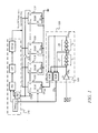
- a multiplying delay-line loop (MDLL) circuit includes a chain of inverting multiplexers 110 with adjustable propagation delay, or "delay multiplexers,” connected in a ring, i.e., such that the output of each delay multiplexer 110 is connected to an input of another delay multiplexer 110.
- the delay multiplexers 110 are designed to be substantially similar.
- One of the delay multiplexers 110 outputs the inverse of the value at a first data input labeled "CK FI " when its enable input, labeled "CK FIEN " is asserted; otherwise the delay multiplexer 110 outputs the inverse of the value at a second data input, labeled "CK FB ".
- the remaining delay multiplexers 110 are wired with the enable input deasserted so that each simply outputs the inverse of its second data input CK FB .
- the output of the final delay multiplexer 110 is connected back to the second data input CK FB of the first delay multiplexer 110.
- An odd number of delay multiplexers 110 may be utilized, so that the chain of delay multiplexers 110 forms a ring oscillator when CK FIEN is not asserted, or an additional inverter 115 (shown in dotted lines in FIG. 1 ) may be used. If the clock signals are differential, this additional inversion may be implemented simply by cross-connecting one pair of differential clock lines between the output of a delay multiplexer and the input of the subsequent delay multiplexer.
- the ring oscillator produces a clock signal referred to as the feedback clock CK FB , at a multiple M of the frequency of the forwarded clock FCK.
- a pulse generator 120 When an edge arrives in the forwarded clock signal FCK, a pulse generator 120 produces a pulse that is applied to the enable input of the first delay multiplexer 110. As a result, the enable input is asserted during the time of the pulse, and during this time, first delay multiplexer 110 substitutes the rising edge of a signal CK FI (also produced by the pulse generator 120) for one edge of the feedback clock CK FB , providing a phase correction to the ring oscillator.
- CK FI is derived from the edge of the forwarded clock signal FCK.
- a first pulse referred to as the feed-in clock pulse CK FI
- a second pulse referred to as the feed-in clock enable pulse CK FIEN
- the forwarded clock is first buffered by buffer 125 to form a buffered forwarded clock signal CK R .
- the two pulses are then formed by a combination of delays and exclusive or (XOR) circuits.
- a first delay circuit 127 with a delay of t d receives the buffered forwarded clock signal CK R and forms a first delayed forwarded clock signal CK R1 .
- This signal is further delayed by a second delay circuit 128 also having a delay of t d , to form a second delayed forwarded clock signal CK R2 .
- the first delay circuit 127 and the second delay circuit 128 may be formed as a chain of buffer, inverters, or other delay producing circuitry.
- the XOR of the first delayed forwarded clock signal CK R1 and the second delayed forwarded clock signal CK R2 then forms the feed-in clock pulse CK FI pulse signal.
- a rising edge of the feed-in clock CK FI follows each rising edge of the forwarded clock FCK by a substantially fixed propagation delay.
- a rising edge of the feed-in clock CK FI follows each falling edge of the forwarded clock FCK by a substantially fixed propagation delay.
- the XOR of the buffered forwarded clock signal CK R and the second delayed forwarded clock signal CK R2 forms feed-in clock enable pulse CK FIEN .
- the use of both clock edges of the forwarded clock to correct the phase of the local clock may reduce the accumulated jitter by half.
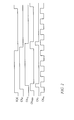
- FIG. 2 shows a timing diagram for the pulse generator.
- the forwarded clock FCK is a square wave
- the first delayed forwarded clock signal CK R1 has substantially the same waveform but is delayed by t d
- the second delayed forwarded clock signal CK R2 also has substantially the same waveform and is delayed by 2 t d .
- the feed-in clock enable pulse CK FIEN is a delayed (as a result of the propagation delay through the XOR circuit) signal that is high when the buffered forwarded clock signal CK R and the second delayed forwarded clock signal CK R2 are at different logic levels.
- the feed-in clock pulse CK FI is a delayed (as a result of the propagation delay through the XOR circuit) signal that is high when the first delayed forwarded clock signal CK R1 and the second delayed forwarded clock signal CK R2 are at different logic levels.
- first and second delay circuits 127, 128 are illustrated as providing the same delay, the delays provided by these two circuits may differ in other embodiments.
- the feed-in clock enable pulse CK FIEN is applied to the enable input of the first delay multiplexer 110, so that the subsequent rising edge of the feed-in clock pulse CK FI is substituted for the rising edge of the delayed forwarded clock signal when an edge arrives in the forwarded clock FCK.
- This rising edge of the feed-in clock pulse CK FI is referred to herein as the "triggering" edge of feed-in clock pulse CK FI because it is the edge that modifies the phase of the feedback clock.
- the CK FI signal and the feedback clock CK FB are supplied to a propagation delay control circuit 140 that controls the phase of the ring oscillator.
- the feed-in clock pulse CK FI is compared, in a phase detector PD, to a signal formed by dividing the feedback clock CK FB by M; the result is fed to a charge pump CP, and filtered by a filter, to form the output V CTRL of the propagation delay control circuit 140.
- This output is connected to a delay control input on each of the delay multiplexers 110.
- the effect of the ring oscillator phase control circuit is to increase the propagation delay of each delay multiplexer 110, thereby decreasing the phase of the feedback clock CK FB , when the edge of the divided feedback clock CK FB precedes the edge of the feed-in clock pulse CK FI , and to decrease the propagation delay of each delay multiplexer 110, thereby increasing the phase of the feedback clock CK FB , when the edge of the feed-in clock pulse CK FI precedes the edge of the divided feedback clock CK FB .
- the charge pump CP may produce a current proportional to a phase difference measured by the phase detector PD, and the filter may provide a loop-shaping function for the control loop these components form around the ring oscillator.
- the bandwidth of the frequency control loop may be controlled by suitable selection of the gains of the phase detector, the charge pump, and the filter of the propagation delay control circuit 140.
- the logic levels of various signals may be reversed.
- the feed-in clock pulse CK FI may be composed of a short pulse of logic low in a signal that is otherwise at a logic high level, and the falling edge of the feed-in clock pulse CK FI may be the triggering edge.
- the delay multiplexers 110 are combined pair-wise to form non-inverting compound delay multiplexers, and the outputs of the compound delay multiplexers (i.e., the outputs consisting of the output of the every other delay multiplexer 110) are sent to the follow-on phase interpolator.
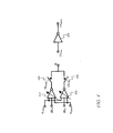
- a delay multiplexer 110 includes three branches 310, 320, 330 each connected between a positive power supply voltage and ground.
- Each branch includes six metal oxide semiconductor field effect transistors (MOSFETs).
- MOSFETs metal oxide semiconductor field effect transistors
- Three p-channel MOSFETs or "PMOS” transistors are connected in series from the positive power supply voltage to the central node 347.
- Three series connected n-channel MOSFETs or "NMOS” transistors are connected in series from the central node to ground.
- the six MOSFETs in each branch form three complementary pairs: a first complementary pair including a PMOS transistor 341 and an NMOS transistor 344, a second complementary pair including a PMOS transistor 342 and an NMOS transistor 345, and third complementary pair including a PMOS transistor 343 and an NMOS transistor 346.
- Each of the three branches 310, 320, 330 acts as a tri-state inverter with a data input, an enable input, which may be a differential input, and a data output, which is the central node 347.
- the first pair of MOSFETS 341, 344 is controlled by the differential enable signal composed of Base EN and its complement Base ENB
- the second pair 342, 345 is controlled by the data signal CK FB . If the enable is high (and its complement is low) then the output of this branch is the inverse of the data signal CK FB .
- the inverter 350 is shown as forming the signal Base ENB from the signal Base EN ; this inverter is illustrated primarily to show the inverse relationship between Base EN and its complement Base ENB , and in other embodiments these two signals may instead be generated concurrently (e.g., substantially simultaneously) as complementary outputs of another circuit.
- the output of the first branch 310 is the inverse of its data input CK FB
- the enable input CK FIEN of the second branch is high and its complement CK FIENB is low
- the output of the second branch 320 is the inverse of its data input CK FI .
- the CK FIEN signal and its complement CK FIENB select whether the first branch 310 or the second branch 320 is active; when CK FIEN is asserted, the second branch 320 is active and the feed-in clock signal CK FI is substituted for the feedback clock signal CK FB .
- the first delay multiplexer 110 is utilized to select when the feed-in clock signal CK FI is substituted for the feedback clock signal CK FB .
- the first delay multiplexer 110 may also be utilized to interpolate between the two clock signals, by asserting the first delay multiplexer's third branch enable signal Base EN (e.g., setting Base EN high and settings its complement Base ENB low).
- Base EN e.g., setting Base EN high and settings its complement Base ENB low.
- the outputs of the second branch 320 and the third branch 330 both contribute to the output 360 of the delay multiplexer 110, if CK FIEN is asserted
- the outputs of the first branch 310 and the third branch 330 both contribute to the output 360 of the delay multiplexer 110 if CK FIEN is not asserted.
- the output 360 of the first delay multiplexer carries only a current controlled by the feed-in clock signal CK FI when CK FIEN is asserted, and it carries only a current controlled by the feedback clock signal CK FB when CK FIEN is deasserted.
- the output 360 of the first delay multiplexer carries an additional current controlled, in the third branch 330, by the feedback clock signal CK FB , regardless of whether CK FIEN is asserted.
- Each of the delay multiplexers 110 of the circuit of FIG. 1 is configured to act as an inverter of the signal received at its CK FB input. This is accomplished by wiring the enable inputs of the first branch 310 to enable the first branch 310 while wiring the enable inputs of the second branch 320 to disable the second branch 320, and connecting the CK FI input to ground.
- the inverter 355 is shown as forming the signal CK FIEN from the signal CK FIENB ; this inverter 355 is illustrated primarily to show the inverse relationship between CK FIEN and its complement CK FIENB . In other embodiments these two signals may instead be generated concurrently (e.g., substantially simultaneously) as complementary outputs of another circuit.
- connections shown in FIG. 1 as a single line may represent more than one conductor, carrying, for example, a differential signal composed of a signal and its complement.
- the terms "input” and “output” as used herein may refer to a single conductor carrying a signal represented as a voltage with respect to ground, or a pair of conductors carrying complementary signals.
- the first pair of MOSFETS 341, 344 is the closest to the central node 347, but the location of this pair of MOSFETS is not limited to this location, and the PMOS transistors in the upper half of any of the three branches 310, 320, 330 may be arranged in a different order, as may the NMOS transmitters in the lower half of any of the three branches 310, 320, 330.
- the relative contributions of the two branches contributing when Base EN is asserted may be tuned at design time by selecting the channels widths of the transistors of the third pair of transistors 343, 346 in the first branch 310 and second branch 320 of the delay multiplexer 110.
- the transistors of the third pair of transistors 343, 346 of the third branch 330 are significantly larger (i.e., have significantly greater channel width) than the transistors of the third pairs of transistors 343, 346 in the other two branches 310, 320 and Base EN is asserted, then the circuit of FIG. 1 approximates that of a phase locked loop (PLL).
- PLL phase locked loop
- the circuit of FIG. 1 approximates (or is about) that of an MDLL.
- the circuit of FIG. 1 is an MDLL with uniformly distributed output phases.
- Diagonal arrows drawn through the transistors 343, 346 of the third pair of the first branch 310 and of the second branch 320 indicate the possibility of designing the circuit with transistor channel widths selected to achieve a desired level of interpolation between the feed-in clock CK FI and the feedback clock CK FB .
- the circuit may be adjusted to provide a compromise between the advantages of a PLL and those of a MDLL, having, for example, better jitter tracking than a PLL would exhibit when there is significant data correlated jitter with the forwarded clock, or better jitter filtering than an MDLL when there is significant data independent jitter with the forwarded clock.
- the control voltages V CTRLP and V CTRLN are applied to the PMOS transistors and the NMOS transistors, respectively, of the third pair of transistors 343, 346 in each of the three branches 310, 320, 330. These transistors are configured to act as continuously variable current control transistors which control the propagation delay through the delay multiplexer 110.
- the lower the voltage V CTRLN and the higher the voltage V CTRLP the longer the propagation delay.
- V CTRLN and V CTRLP control the extent to which these transistors limit the current in the three branches and the rate at which the voltage at the output of the delay multiplexer 110 is changed, , thereby adjusting the propagation delay of the subsequent delay multiplexer 110.
- the inputs V CTRLN and V CTRLP may be utilized as delay control inputs to which the output of the propagation delay control circuit 140 may be connected.
- the transistors of the third pair of transistors 343, 346 may be compound transistors with effective channel widths that may be adjusted after fabrication, e.g., at run time.
- a compound transistor may be formed, for example, as an array of current control transistors, each connected in series with a switching transistor. Each of the series combinations is then connected in parallel.
- the effective channel width of the compound transistor is then the sum of the channel widths of the current control transistors in the array that are enabled (as a result of their respective switching transistors being turned on).
- a delay multiplexer 110 is implemented with two inverters 410, 420, each having a propagation delay controlled by the control voltages V CTRLN and V CTRLP , the output of the delay multiplexer being selected from the outputs of the two inverters using a pair of switches 430, 440 controlled by the feed-in clock enable signal CK FIEN signal and its complement CK FIENB .
- the inverter 355 is shown as forming the signal CK FIEN from the signal CK FIENB ; this inverter is illustrated primarily to show the inverse relationship between CK FIEN and its complement CK FIENB , and in other embodiments these two signals may instead be generated concurrently (e.g., substantially simultaneously) as complementary outputs of another circuit.
- a display 500 includes a timing controller 510 and a driver integrated circuit (IC) 520, and the timing controller 510 is configured to send high-speed serial data on a data lane 530, with an accompanying forwarded clock on a clock lane 540, to the driver IC 520.
- the forwarded clock is a reduced-frequency clock
- the driver IC generates an internal high-speed clock using a MDLL/PLL circuit 550 constructed according to an embodiment of the present invention.
- the display is an organic light emitting diode (OLED) display or a liquid crystal display (LCD).
Landscapes
- Engineering & Computer Science (AREA)
- Physics & Mathematics (AREA)
- Computer Hardware Design (AREA)
- General Physics & Mathematics (AREA)
- Theoretical Computer Science (AREA)
- Nonlinear Science (AREA)
- Chemical & Material Sciences (AREA)
- Crystallography & Structural Chemistry (AREA)
- Multimedia (AREA)
- Pulse Circuits (AREA)
- Stabilization Of Oscillater, Synchronisation, Frequency Synthesizers (AREA)
Applications Claiming Priority (2)
| Application Number | Priority Date | Filing Date | Title |
|---|---|---|---|
| US201461934641P | 2014-01-31 | 2014-01-31 | |
| US14/593,977 US9685141B2 (en) | 2014-01-31 | 2015-01-09 | MDLL/PLL hybrid design with uniformly distributed output phases |
Publications (3)
| Publication Number | Publication Date |
|---|---|
| EP2903162A2 true EP2903162A2 (de) | 2015-08-05 |
| EP2903162A3 EP2903162A3 (de) | 2015-11-25 |
| EP2903162B1 EP2903162B1 (de) | 2021-04-07 |
Family
ID=52449968
Family Applications (1)
| Application Number | Title | Priority Date | Filing Date |
|---|---|---|---|
| EP15152877.5A Active EP2903162B1 (de) | 2014-01-31 | 2015-01-28 | Hybrides MDLL/PLL-Design mit gleichförmig verteilten Ausgangsphasen |
Country Status (3)
| Country | Link |
|---|---|
| US (1) | US9685141B2 (de) |
| EP (1) | EP2903162B1 (de) |
| CN (1) | CN104821822B (de) |
Families Citing this family (22)
| Publication number | Priority date | Publication date | Assignee | Title |
|---|---|---|---|---|
| DE112015001133T5 (de) * | 2014-03-07 | 2016-12-01 | Semiconductor Energy Laboratory Co., Ltd. | Betriebsverfahren für eine Halbleitervorrichtung |
| KR101970845B1 (ko) * | 2014-11-20 | 2019-08-13 | 에스케이하이닉스 주식회사 | 반도체 장치 |
| KR20170049193A (ko) * | 2015-10-28 | 2017-05-10 | 삼성전자주식회사 | 지연 고정 루프회로 및 이를 포함하는 반도체 메모리 장치 |
| CN105680869A (zh) * | 2016-01-29 | 2016-06-15 | 成都科创谷科技有限公司 | 一种基于瞬时电压抑制的缓冲串行电路 |
| TWI730091B (zh) | 2016-05-13 | 2021-06-11 | 日商半導體能源研究所股份有限公司 | 半導體裝置 |
| US9825636B1 (en) * | 2016-10-20 | 2017-11-21 | Arm Limited | Apparatus and method for reduced latency signal synchronization |
| US10164649B2 (en) | 2016-11-30 | 2018-12-25 | Taiwan Semiconductor Manufacturing Co., Ltd. | Hybrid phase lock loop |
| CN106849942B (zh) * | 2016-12-29 | 2020-10-16 | 北京时代民芯科技有限公司 | 一种超高速低抖动多相位时钟电路 |
| US10840916B2 (en) | 2017-08-07 | 2020-11-17 | Intel Corporation | Multiplying delay lock loop (MDLL) and method of averaging ring oscillator signals for jitter compensation |
| KR102528561B1 (ko) * | 2018-05-09 | 2023-05-04 | 삼성전자주식회사 | 클락 생성을 위한 장치 및 방법 |
| CN108964658A (zh) * | 2018-06-25 | 2018-12-07 | 哈尔滨工业大学 | 基于锁相环和标准尺延迟线的时钟发生装置及其实现方法 |
| TWI697883B (zh) * | 2019-03-28 | 2020-07-01 | 聚積科技股份有限公司 | 顯示系統及其驅動電路 |
| US11296684B2 (en) * | 2020-03-31 | 2022-04-05 | Taiwan Semiconductor Manufacturing Company, Ltd. | Gated tri-state inverter, and low power reduced area phase interpolator system including same, and method of operating same |
| KR102769511B1 (ko) * | 2020-04-09 | 2025-02-19 | 에스케이하이닉스 주식회사 | 지연 회로 및 위상 보간기 |
| US12143113B2 (en) | 2020-04-09 | 2024-11-12 | SK Hynix Inc. | Integrated circuit and memory system |
| KR102738531B1 (ko) * | 2020-05-11 | 2024-12-06 | 주식회사 엘엑스세미콘 | 화소의 구동을 위한 클럭생성장치 및 이를 포함하는 디스플레이장치 |
| US11218140B1 (en) * | 2020-08-26 | 2022-01-04 | Apple Inc. | Cross-phase detector based phase interpolator |
| US11641206B2 (en) * | 2021-01-07 | 2023-05-02 | AyDeeKay LLC | Digitally calibrated programmable clock phase generation circuit |
| US11489518B2 (en) * | 2021-03-05 | 2022-11-01 | Qualcomm Incorporated | Inverter-based delay element with adjustable current source/sink to reduce delay sensitivity to process and supply voltage variation |
| US12369238B2 (en) * | 2023-01-31 | 2025-07-22 | Avago Technologies International Sales Pte. Limited | LED driver electromagnetic interference mitigation |
| CN117133230B (zh) * | 2023-10-26 | 2024-01-26 | 成都利普芯微电子有限公司 | Led显示驱动芯片及共阴led显示系统、共阳led显示系统 |
| US12483250B2 (en) * | 2024-02-22 | 2025-11-25 | Analog Devices International Unlimited Company | Multiplying delay locked loop with high tolerance to input jitter |
Family Cites Families (19)
| Publication number | Priority date | Publication date | Assignee | Title |
|---|---|---|---|---|
| US6208183B1 (en) | 1999-04-30 | 2001-03-27 | Conexant Systems, Inc. | Gated delay-locked loop for clock generation applications |
| US20020051511A1 (en) | 2000-10-31 | 2002-05-02 | Nec Viewtechnology, Ltd. | Video apparatus having serial receiver |
| US6617936B2 (en) | 2001-02-20 | 2003-09-09 | Velio Communications, Inc. | Phase controlled oscillator |
| JP4158465B2 (ja) * | 2002-09-10 | 2008-10-01 | 日本電気株式会社 | クロック再生装置、および、クロック再生装置を用いた電子機器 |
| US6788119B1 (en) * | 2003-03-27 | 2004-09-07 | Xilinx, Inc. | Delay line circuit providing clock pulse width restoration in delay lock loops |
| US7237164B1 (en) * | 2004-04-15 | 2007-06-26 | Marvell International Ltd. | Area optimized edge-triggered flip-flop for high-speed memory dominated design |
| US7525363B2 (en) * | 2006-09-01 | 2009-04-28 | Via Technologies, Inc. | Delay line and delay lock loop |
| KR100822307B1 (ko) | 2007-09-20 | 2008-04-16 | 주식회사 아나패스 | 데이터 구동 회로 및 지연 고정 루프 |
| JP4990315B2 (ja) * | 2008-03-20 | 2012-08-01 | アナパス・インコーポレーテッド | ブランク期間にクロック信号を伝送するディスプレイ装置及び方法 |
| US7821298B2 (en) * | 2008-08-10 | 2010-10-26 | Eric Mahurin | Multiplexing using product-of-sums and sum-of-products |
| JP2010136002A (ja) * | 2008-12-03 | 2010-06-17 | Renesas Electronics Corp | 遅延回路 |
| KR101012678B1 (ko) | 2009-02-04 | 2011-02-09 | 연세대학교 산학협력단 | 지연 동기 루프 및 이를 포함하는 전자 장치 |
| US8169243B2 (en) | 2009-04-02 | 2012-05-01 | Qualcomm Incorporated | Techniques for non-overlapping clock generation |
| US7994832B2 (en) * | 2009-11-06 | 2011-08-09 | Oracle America, Inc. | Aperture generating circuit for a multiplying delay-locked loop |
| US8704805B2 (en) | 2010-04-19 | 2014-04-22 | Himax Technologies Limited | System and method for handling image data transfer in a display driver |
| CN102545838B (zh) * | 2011-10-21 | 2015-02-04 | 嘉兴联星微电子有限公司 | 一种超低功耗的时钟产生器 |
| KR101459696B1 (ko) | 2013-04-16 | 2014-11-12 | (주)유에스 | 전동식 정형용 다리관절 운동장치 |
| US9024658B2 (en) * | 2013-05-29 | 2015-05-05 | Qualcomm Incorporated | Circuit and layout techniques for flop tray area and power otimization |
| US9191128B2 (en) * | 2013-12-17 | 2015-11-17 | National Applied Research Laboratories | Spread spectrum clock generator and method for generating spread spectrum clock signal |
-
2015
- 2015-01-09 US US14/593,977 patent/US9685141B2/en active Active
- 2015-01-28 EP EP15152877.5A patent/EP2903162B1/de active Active
- 2015-01-30 CN CN201510049972.4A patent/CN104821822B/zh active Active
Non-Patent Citations (1)
| Title |
|---|
| None |
Also Published As
| Publication number | Publication date |
|---|---|
| CN104821822B (zh) | 2020-01-17 |
| US20150221285A1 (en) | 2015-08-06 |
| CN104821822A (zh) | 2015-08-05 |
| EP2903162A3 (de) | 2015-11-25 |
| EP2903162B1 (de) | 2021-04-07 |
| US9685141B2 (en) | 2017-06-20 |
Similar Documents
| Publication | Publication Date | Title |
|---|---|---|
| US9685141B2 (en) | MDLL/PLL hybrid design with uniformly distributed output phases | |
| US6600355B1 (en) | Clock generator circuit providing an output clock signal from phased input clock signals | |
| US10326457B2 (en) | Reference-locked clock generator | |
| US10038433B2 (en) | Device for correcting multi-phase clock signal | |
| JP3575430B2 (ja) | 2段階可変長遅延回路 | |
| US6909317B2 (en) | Clock control circuit and method | |
| US7932766B2 (en) | Digitally controlled oscillator with the wide operation range | |
| EP3292631B1 (de) | Programmierbare verzögerungsschaltung für anwendungen mit niedrigem stromverbrauch | |
| US20090267698A1 (en) | Dual supply inverter for voltage controlled ring oscillator | |
| US7323918B1 (en) | Mutual-interpolating delay-locked loop for high-frequency multiphase clock generation | |
| US6788119B1 (en) | Delay line circuit providing clock pulse width restoration in delay lock loops | |
| US9742413B2 (en) | Electronic device and information processing apparatus | |
| EP3267585B1 (de) | Phasendetektor für eine taktdatenwiederherstellungsschaltung | |
| US9350338B2 (en) | Linear progression delay register | |
| US20120057606A1 (en) | Multiplexer circuit | |
| US20210159892A1 (en) | Time-delay circuit for a digital signal, particularly for a clock signal | |
| US20180309456A1 (en) | Phase combiner circuit | |
| KR100506952B1 (ko) | 클럭 제어회로 및 방법 | |
| JP2010288005A (ja) | 遅延同期ループ回路およびインターフェース回路 | |
| US9252759B1 (en) | Linear progression delay register | |
| KR100833591B1 (ko) | 위상 동기 장치 및 위상 동기 신호 생성 방법 |
Legal Events
| Date | Code | Title | Description |
|---|---|---|---|
| PUAI | Public reference made under article 153(3) epc to a published international application that has entered the european phase |
Free format text: ORIGINAL CODE: 0009012 |
|
| 17P | Request for examination filed |
Effective date: 20150128 |
|
| AK | Designated contracting states |
Kind code of ref document: A2 Designated state(s): AL AT BE BG CH CY CZ DE DK EE ES FI FR GB GR HR HU IE IS IT LI LT LU LV MC MK MT NL NO PL PT RO RS SE SI SK SM TR |
|
| AX | Request for extension of the european patent |
Extension state: BA ME |
|
| RAP1 | Party data changed (applicant data changed or rights of an application transferred) |
Owner name: SAMSUNG DISPLAY CO., LTD. |
|
| PUAL | Search report despatched |
Free format text: ORIGINAL CODE: 0009013 |
|
| AK | Designated contracting states |
Kind code of ref document: A3 Designated state(s): AL AT BE BG CH CY CZ DE DK EE ES FI FR GB GR HR HU IE IS IT LI LT LU LV MC MK MT NL NO PL PT RO RS SE SI SK SM TR |
|
| AX | Request for extension of the european patent |
Extension state: BA ME |
|
| RIC1 | Information provided on ipc code assigned before grant |
Ipc: H03L 7/081 20060101AFI20151020BHEP Ipc: H03L 7/099 20060101ALI20151020BHEP |
|
| 17P | Request for examination filed |
Effective date: 20160519 |
|
| RBV | Designated contracting states (corrected) |
Designated state(s): AL AT BE BG CH CY CZ DE DK EE ES FI FR GB GR HR HU IE IS IT LI LT LU LV MC MK MT NL NO PL PT RO RS SE SI SK SM TR |
|
| STAA | Information on the status of an ep patent application or granted ep patent |
Free format text: STATUS: EXAMINATION IS IN PROGRESS |
|
| 17Q | First examination report despatched |
Effective date: 20191009 |
|
| GRAP | Despatch of communication of intention to grant a patent |
Free format text: ORIGINAL CODE: EPIDOSNIGR1 |
|
| STAA | Information on the status of an ep patent application or granted ep patent |
Free format text: STATUS: GRANT OF PATENT IS INTENDED |
|
| INTG | Intention to grant announced |
Effective date: 20201209 |
|
| GRAS | Grant fee paid |
Free format text: ORIGINAL CODE: EPIDOSNIGR3 |
|
| GRAA | (expected) grant |
Free format text: ORIGINAL CODE: 0009210 |
|
| STAA | Information on the status of an ep patent application or granted ep patent |
Free format text: STATUS: THE PATENT HAS BEEN GRANTED |
|
| AK | Designated contracting states |
Kind code of ref document: B1 Designated state(s): AL AT BE BG CH CY CZ DE DK EE ES FI FR GB GR HR HU IE IS IT LI LT LU LV MC MK MT NL NO PL PT RO RS SE SI SK SM TR |
|
| REG | Reference to a national code |
Ref country code: GB Ref legal event code: FG4D |
|
| REG | Reference to a national code |
Ref country code: AT Ref legal event code: REF Ref document number: 1381003 Country of ref document: AT Kind code of ref document: T Effective date: 20210415 Ref country code: CH Ref legal event code: EP |
|
| REG | Reference to a national code |
Ref country code: DE Ref legal event code: R096 Ref document number: 602015067669 Country of ref document: DE |
|
| REG | Reference to a national code |
Ref country code: IE Ref legal event code: FG4D |
|
| REG | Reference to a national code |
Ref country code: LT Ref legal event code: MG9D |
|
| REG | Reference to a national code |
Ref country code: NL Ref legal event code: MP Effective date: 20210407 Ref country code: AT Ref legal event code: MK05 Ref document number: 1381003 Country of ref document: AT Kind code of ref document: T Effective date: 20210407 |
|
| PG25 | Lapsed in a contracting state [announced via postgrant information from national office to epo] |
Ref country code: HR Free format text: LAPSE BECAUSE OF FAILURE TO SUBMIT A TRANSLATION OF THE DESCRIPTION OR TO PAY THE FEE WITHIN THE PRESCRIBED TIME-LIMIT Effective date: 20210407 Ref country code: BG Free format text: LAPSE BECAUSE OF FAILURE TO SUBMIT A TRANSLATION OF THE DESCRIPTION OR TO PAY THE FEE WITHIN THE PRESCRIBED TIME-LIMIT Effective date: 20210707 Ref country code: AT Free format text: LAPSE BECAUSE OF FAILURE TO SUBMIT A TRANSLATION OF THE DESCRIPTION OR TO PAY THE FEE WITHIN THE PRESCRIBED TIME-LIMIT Effective date: 20210407 Ref country code: NL Free format text: LAPSE BECAUSE OF FAILURE TO SUBMIT A TRANSLATION OF THE DESCRIPTION OR TO PAY THE FEE WITHIN THE PRESCRIBED TIME-LIMIT Effective date: 20210407 Ref country code: LT Free format text: LAPSE BECAUSE OF FAILURE TO SUBMIT A TRANSLATION OF THE DESCRIPTION OR TO PAY THE FEE WITHIN THE PRESCRIBED TIME-LIMIT Effective date: 20210407 Ref country code: FI Free format text: LAPSE BECAUSE OF FAILURE TO SUBMIT A TRANSLATION OF THE DESCRIPTION OR TO PAY THE FEE WITHIN THE PRESCRIBED TIME-LIMIT Effective date: 20210407 |
|
| PG25 | Lapsed in a contracting state [announced via postgrant information from national office to epo] |
Ref country code: IS Free format text: LAPSE BECAUSE OF FAILURE TO SUBMIT A TRANSLATION OF THE DESCRIPTION OR TO PAY THE FEE WITHIN THE PRESCRIBED TIME-LIMIT Effective date: 20210807 Ref country code: LV Free format text: LAPSE BECAUSE OF FAILURE TO SUBMIT A TRANSLATION OF THE DESCRIPTION OR TO PAY THE FEE WITHIN THE PRESCRIBED TIME-LIMIT Effective date: 20210407 Ref country code: GR Free format text: LAPSE BECAUSE OF FAILURE TO SUBMIT A TRANSLATION OF THE DESCRIPTION OR TO PAY THE FEE WITHIN THE PRESCRIBED TIME-LIMIT Effective date: 20210708 Ref country code: RS Free format text: LAPSE BECAUSE OF FAILURE TO SUBMIT A TRANSLATION OF THE DESCRIPTION OR TO PAY THE FEE WITHIN THE PRESCRIBED TIME-LIMIT Effective date: 20210407 Ref country code: SE Free format text: LAPSE BECAUSE OF FAILURE TO SUBMIT A TRANSLATION OF THE DESCRIPTION OR TO PAY THE FEE WITHIN THE PRESCRIBED TIME-LIMIT Effective date: 20210407 Ref country code: NO Free format text: LAPSE BECAUSE OF FAILURE TO SUBMIT A TRANSLATION OF THE DESCRIPTION OR TO PAY THE FEE WITHIN THE PRESCRIBED TIME-LIMIT Effective date: 20210707 Ref country code: PL Free format text: LAPSE BECAUSE OF FAILURE TO SUBMIT A TRANSLATION OF THE DESCRIPTION OR TO PAY THE FEE WITHIN THE PRESCRIBED TIME-LIMIT Effective date: 20210407 Ref country code: PT Free format text: LAPSE BECAUSE OF FAILURE TO SUBMIT A TRANSLATION OF THE DESCRIPTION OR TO PAY THE FEE WITHIN THE PRESCRIBED TIME-LIMIT Effective date: 20210809 Ref country code: ES Free format text: LAPSE BECAUSE OF FAILURE TO SUBMIT A TRANSLATION OF THE DESCRIPTION OR TO PAY THE FEE WITHIN THE PRESCRIBED TIME-LIMIT Effective date: 20210407 |
|
| REG | Reference to a national code |
Ref country code: DE Ref legal event code: R097 Ref document number: 602015067669 Country of ref document: DE |
|
| PG25 | Lapsed in a contracting state [announced via postgrant information from national office to epo] |
Ref country code: SK Free format text: LAPSE BECAUSE OF FAILURE TO SUBMIT A TRANSLATION OF THE DESCRIPTION OR TO PAY THE FEE WITHIN THE PRESCRIBED TIME-LIMIT Effective date: 20210407 Ref country code: SM Free format text: LAPSE BECAUSE OF FAILURE TO SUBMIT A TRANSLATION OF THE DESCRIPTION OR TO PAY THE FEE WITHIN THE PRESCRIBED TIME-LIMIT Effective date: 20210407 Ref country code: CZ Free format text: LAPSE BECAUSE OF FAILURE TO SUBMIT A TRANSLATION OF THE DESCRIPTION OR TO PAY THE FEE WITHIN THE PRESCRIBED TIME-LIMIT Effective date: 20210407 Ref country code: DK Free format text: LAPSE BECAUSE OF FAILURE TO SUBMIT A TRANSLATION OF THE DESCRIPTION OR TO PAY THE FEE WITHIN THE PRESCRIBED TIME-LIMIT Effective date: 20210407 Ref country code: EE Free format text: LAPSE BECAUSE OF FAILURE TO SUBMIT A TRANSLATION OF THE DESCRIPTION OR TO PAY THE FEE WITHIN THE PRESCRIBED TIME-LIMIT Effective date: 20210407 Ref country code: RO Free format text: LAPSE BECAUSE OF FAILURE TO SUBMIT A TRANSLATION OF THE DESCRIPTION OR TO PAY THE FEE WITHIN THE PRESCRIBED TIME-LIMIT Effective date: 20210407 |
|
| PLBE | No opposition filed within time limit |
Free format text: ORIGINAL CODE: 0009261 |
|
| STAA | Information on the status of an ep patent application or granted ep patent |
Free format text: STATUS: NO OPPOSITION FILED WITHIN TIME LIMIT |
|
| 26N | No opposition filed |
Effective date: 20220110 |
|
| PG25 | Lapsed in a contracting state [announced via postgrant information from national office to epo] |
Ref country code: IS Free format text: LAPSE BECAUSE OF FAILURE TO SUBMIT A TRANSLATION OF THE DESCRIPTION OR TO PAY THE FEE WITHIN THE PRESCRIBED TIME-LIMIT Effective date: 20210807 Ref country code: AL Free format text: LAPSE BECAUSE OF FAILURE TO SUBMIT A TRANSLATION OF THE DESCRIPTION OR TO PAY THE FEE WITHIN THE PRESCRIBED TIME-LIMIT Effective date: 20210407 |
|
| PG25 | Lapsed in a contracting state [announced via postgrant information from national office to epo] |
Ref country code: IT Free format text: LAPSE BECAUSE OF FAILURE TO SUBMIT A TRANSLATION OF THE DESCRIPTION OR TO PAY THE FEE WITHIN THE PRESCRIBED TIME-LIMIT Effective date: 20210407 |
|
| PG25 | Lapsed in a contracting state [announced via postgrant information from national office to epo] |
Ref country code: MC Free format text: LAPSE BECAUSE OF FAILURE TO SUBMIT A TRANSLATION OF THE DESCRIPTION OR TO PAY THE FEE WITHIN THE PRESCRIBED TIME-LIMIT Effective date: 20210407 |
|
| REG | Reference to a national code |
Ref country code: CH Ref legal event code: PL |
|
| REG | Reference to a national code |
Ref country code: BE Ref legal event code: MM Effective date: 20220131 |
|
| PG25 | Lapsed in a contracting state [announced via postgrant information from national office to epo] |
Ref country code: LU Free format text: LAPSE BECAUSE OF NON-PAYMENT OF DUE FEES Effective date: 20220128 |
|
| PG25 | Lapsed in a contracting state [announced via postgrant information from national office to epo] |
Ref country code: BE Free format text: LAPSE BECAUSE OF NON-PAYMENT OF DUE FEES Effective date: 20220131 |
|
| PG25 | Lapsed in a contracting state [announced via postgrant information from national office to epo] |
Ref country code: LI Free format text: LAPSE BECAUSE OF NON-PAYMENT OF DUE FEES Effective date: 20220131 Ref country code: CH Free format text: LAPSE BECAUSE OF NON-PAYMENT OF DUE FEES Effective date: 20220131 |
|
| PG25 | Lapsed in a contracting state [announced via postgrant information from national office to epo] |
Ref country code: IE Free format text: LAPSE BECAUSE OF NON-PAYMENT OF DUE FEES Effective date: 20220128 |
|
| P01 | Opt-out of the competence of the unified patent court (upc) registered |
Effective date: 20230516 |
|
| PG25 | Lapsed in a contracting state [announced via postgrant information from national office to epo] |
Ref country code: HU Free format text: LAPSE BECAUSE OF FAILURE TO SUBMIT A TRANSLATION OF THE DESCRIPTION OR TO PAY THE FEE WITHIN THE PRESCRIBED TIME-LIMIT; INVALID AB INITIO Effective date: 20150128 |
|
| PG25 | Lapsed in a contracting state [announced via postgrant information from national office to epo] |
Ref country code: MK Free format text: LAPSE BECAUSE OF FAILURE TO SUBMIT A TRANSLATION OF THE DESCRIPTION OR TO PAY THE FEE WITHIN THE PRESCRIBED TIME-LIMIT Effective date: 20210407 Ref country code: CY Free format text: LAPSE BECAUSE OF FAILURE TO SUBMIT A TRANSLATION OF THE DESCRIPTION OR TO PAY THE FEE WITHIN THE PRESCRIBED TIME-LIMIT Effective date: 20210407 |
|
| PG25 | Lapsed in a contracting state [announced via postgrant information from national office to epo] |
Ref country code: MT Free format text: LAPSE BECAUSE OF FAILURE TO SUBMIT A TRANSLATION OF THE DESCRIPTION OR TO PAY THE FEE WITHIN THE PRESCRIBED TIME-LIMIT Effective date: 20210407 |
|
| PG25 | Lapsed in a contracting state [announced via postgrant information from national office to epo] |
Ref country code: TR Free format text: LAPSE BECAUSE OF FAILURE TO SUBMIT A TRANSLATION OF THE DESCRIPTION OR TO PAY THE FEE WITHIN THE PRESCRIBED TIME-LIMIT Effective date: 20210407 |
|
| PGFP | Annual fee paid to national office [announced via postgrant information from national office to epo] |
Ref country code: GB Payment date: 20251222 Year of fee payment: 12 |
|
| PGFP | Annual fee paid to national office [announced via postgrant information from national office to epo] |
Ref country code: FR Payment date: 20251223 Year of fee payment: 12 |
|
| PGFP | Annual fee paid to national office [announced via postgrant information from national office to epo] |
Ref country code: DE Payment date: 20251222 Year of fee payment: 12 |