EP2899884A2 - Verfahren zur Erzeugung eines Taktes für ein mit steigender Flanke betriebenes System - Google Patents
Verfahren zur Erzeugung eines Taktes für ein mit steigender Flanke betriebenes System Download PDFInfo
- Publication number
- EP2899884A2 EP2899884A2 EP14193374.7A EP14193374A EP2899884A2 EP 2899884 A2 EP2899884 A2 EP 2899884A2 EP 14193374 A EP14193374 A EP 14193374A EP 2899884 A2 EP2899884 A2 EP 2899884A2
- Authority
- EP
- European Patent Office
- Prior art keywords
- value
- clock
- input clock
- rising edge
- output clock
- Prior art date
- Legal status (The legal status is an assumption and is not a legal conclusion. Google has not performed a legal analysis and makes no representation as to the accuracy of the status listed.)
- Withdrawn
Links
Images


Classifications
-
- G—PHYSICS
- G06—COMPUTING OR CALCULATING; COUNTING
- G06F—ELECTRIC DIGITAL DATA PROCESSING
- G06F1/00—Details not covered by groups G06F3/00 - G06F13/00 and G06F21/00
- G06F1/04—Generating or distributing clock signals or signals derived directly therefrom
- G06F1/08—Clock generators with changeable or programmable clock frequency
-
- H—ELECTRICITY
- H03—ELECTRONIC CIRCUITRY
- H03K—PULSE TECHNIQUE
- H03K3/00—Circuits for generating electric pulses; Monostable, bistable or multistable circuits
-
- H—ELECTRICITY
- H03—ELECTRONIC CIRCUITRY
- H03K—PULSE TECHNIQUE
- H03K5/00—Manipulating of pulses not covered by one of the other main groups of this subclass
- H03K5/153—Arrangements in which a pulse is delivered at the instant when a predetermined characteristic of an input signal is present or at a fixed time interval after this instant
- H03K5/1534—Transition or edge detectors
-
- H—ELECTRICITY
- H03—ELECTRONIC CIRCUITRY
- H03K—PULSE TECHNIQUE
- H03K23/00—Pulse counters comprising counting chains; Frequency dividers comprising counting chains
- H03K23/64—Pulse counters comprising counting chains; Frequency dividers comprising counting chains with a base or radix other than a power of two
- H03K23/68—Pulse counters comprising counting chains; Frequency dividers comprising counting chains with a base or radix other than a power of two with a base which is a non-integer
Definitions
- the present disclosure relates to a method of generating a clock operating at a rising edge and more particularly, to a method of generating a clock signal in a simple structure at high precision.
- the clock signal is a square wave signal in which logic states '1' and '0' are regularly represented.
- a clock has a certain duty ratio and the system is synchronized with the clock to process various signals.
- a clock generation device may be a device that generates a clock having a certain duty ratio to be used in a system and may include a PLL circuit.
- the PLL circuit has limitations in that its logic is complex and it needs many transistors.
- Fig. 1 shows how to provide a system needing a clock having a certain duty ratio with a clock.
- a PLL circuit 11 adjusts an input clock and generates an output clock suitable for a system 12.
- the PLL circuit may be implemented in both hardware and software, and since a hardware PLL structure has high precision but is complex in logic structure, it needs many transistors. On the contrary, a software-type PLL structure has a limitation in that it is difficult to ensure the precision of an output clock.
- a clock adjustment by the PLL circuit is needed but a system that operates only at the rising edge or falling edge of the clock does not need a PLL circuit having a complex structure.
- generating the clock precisely is needed.
- Embodiments provide a method of generating a clock at high precision through a simple structure, in the case of a system that operates in the rising edge of the clock.
- a method of converting an input clock to generate an output clock and providing a certain system with the output clock includes setting up a desired output clock value and a variable value and determining whether the input clock is the rising edge; adding the output clock value to the variable value to provide a calculated value when the input clock is the rising edge; comparing the calculated value with the input clock value; and outputting, when the calculated value is equal to or larger than the input clock value as a result of comparison, the output clock as logic state '1' and setting, a value obtained by subtracting the input clock value from the calculated value, as the variable value.
- the output clock value may be set to be smaller than the frequency of the input clock.
- the determining of whether the input clock is the rising edge may include continually checking whether the input clock is the rising edge, when the input clock is not the rising edge.
- variable value When the calculated value is smaller than the input clock value as a result of comparison, the variable value may be set with the calculated value and then it may be checked whether the input clock is the rising edge.
- the output clock may be output with logic state '1' and then with logic state '0' at the rising edge of the input clock.
- variable value may be initially set to 0, and in this case, the output clock may be set as logic state '0'.
- the method may further include determining whether the input clock is the rising edge, after the setting of the value obtained by subtracting the input clock value from the calculated value as the variable value.
- Fig. 2 shows an example of where a clock generation device according to an embodiment is used
- Fig. 3 shows a configuration of a clock generation device for a system operating at a rising edge according to an embodiment.
- a clock generation device according to an embodiment is applied to a system that operates by a rising edge.
- a clock generation device 110 changes an input clock to be suitable for a system 120 and provides the system 120 with a generated output clock.
- the clock generation device 110 may include an output clock setup unit 11 and an output clock generation unit 113.
- the output clock setup unit 111 is used for setting up an output clock to be provided for the system 120 and may be a user interface with which a user set up an output clock. For example, it may include an input screen that is shown on a display to be able to input an output clock, and an input unit such as a keyboard.
- a user may input a desired output clock to the input screen shown on the display by using a keyboard to set up the output clock.
- the output clock since the output clock is generated by using the rising edge of an input clock in the present embodiment, the output clock may be set to be smaller than the input clock.
- the unit of a value set up for the output clock setup unit 111 is a frequency.
- the output clock generation unit 113 changes the frequency of the input clock based on a setup value set by the output clock setup unit 111 and generates the output clock.
- the operation of the output clock generation unit 113 is described with reference to Figs. 4 and 5 .
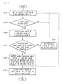
- Fig. 4 is a flowchart of the operation of a clock generation device for a system operating at a rising edge according to an embodiment.
- a desired output clock value N and a variable value N' are firstly set up in step S110.
- the output clock value N is set up to be smaller than an input clock value M.
- the output clock value is set up through the output clock setup unit 111 and the variable value N' is initially set to '0'.
- the output clock generation unit 113 receives the output clock value set up by the output clock setup unit 111 and an input clock, converts the frequency of the input clock based on the output clock value, then generates and outputs the output clock.
- step S120 it is determined whether the input clock is a rising edge in step S120, and when negative, it is continually checked whether the input clock is the rising edge.
- the output clock is initially set with logic state '0'.
- the output clock generation unit 113 adds the variable value N' to the output clock value N to generate a calculated value N" in step S130.
- step S140 the input clock value M is compared with the calculated value N" in step S140, and when the latter is smaller than the former (No in step S140), the variable value N' is set with the calculated value N" in step S150. In addition, it is again determined whether the input clock is the rising edge in step S120.
- the output clock generation unit 113 When the calculated value N" is equal to or larger than the input clock value M (Yes in step S140), the output clock generation unit 113 generates the output clock of logic state '1' for a certain time and sets, a value obtained by subtracting the input clock value M from the calculated value N", as the variable value N' in step S160.
- step S120 it is determined whether the input clock is the rising edge in step S120, and by repetitively performing such an operation, an output clock converted into a frequency set as an output setup value.
- a time period during which the logic state '1' of the output clock is maintained is the same as the width of logic state '1' of the input clock. That is, the output state of the output clock maintains logic state '1' and then changes to logic state '0' as at the falling edge of the input clock.
- the output clock generation unit 113 maintains the output clock at logic state '1' and outputs the output clock with logic state '0' at the falling edge of the input clock, in step S170.
- Fig. 5 is an exemplary waveform diagram of an output clock that is generated by a method of generating a clock for a system operating at a rising edge according to an embodiment.
- Fig. 5 shows that the input clock value M is 300 MHz and the output clock value N is 100 MHz.
- the output clock value N is initially set to 100 and the variable value N' is initially set to 0 in step S110, the output clock value N '100' is added to the variable value N' '0' to provide a calculated value N" '100' in step S130.
- the input clock value M '300' is compared with the calculated value N" '100' in step S140, and since the latter M is smaller than the former N" (No in step S140), the variable value N' is set with the calculated value N" in step S150. Thus, the variable value N' becomes 100 and then it is determined whether the input clock is the rising edge in step S120.
- the input clock value M '300' is compared with the calculated value N" '200' in step S140, and since the former M is larger than the latter N" (No in step S140), the variable value N' is set with the calculated value N" in step S150, the variable value N' becomes 200 and then it is determined whether the input clock is the rising edge in step S120.
- the output clock value N '100' is added to the variable value N' '200' to provide a calculated value N" '300' in step S130.
- the input clock value M '300' is compared with the calculated value N" '300' in step S140, and since the former M is equal to the latter N" (Yes in step S140), the output clock is output as logic state '1' and zero obtained by subtracting the input clock value M '300' from the calculated value N" '300' is set as the variable value N' in step S160.
- step S120 it is again determined whether the input clock is a rising edge in step S120, and as such a process is repeated, an output clock is generated.
- the output clock maintains logic state '1' and then logic state '0' at the falling edge of the input clock in step S170.
Landscapes
- Physics & Mathematics (AREA)
- Engineering & Computer Science (AREA)
- Theoretical Computer Science (AREA)
- Nonlinear Science (AREA)
- General Engineering & Computer Science (AREA)
- General Physics & Mathematics (AREA)
- Synchronisation In Digital Transmission Systems (AREA)
- Manipulation Of Pulses (AREA)
- Stabilization Of Oscillater, Synchronisation, Frequency Synthesizers (AREA)
Applications Claiming Priority (1)
| Application Number | Priority Date | Filing Date | Title |
|---|---|---|---|
| KR1020140009486A KR101682272B1 (ko) | 2014-01-27 | 2014-01-27 | 상승 에지 동작 시스템용 클럭 생성방법 |
Publications (2)
| Publication Number | Publication Date |
|---|---|
| EP2899884A2 true EP2899884A2 (de) | 2015-07-29 |
| EP2899884A3 EP2899884A3 (de) | 2015-10-21 |
Family
ID=51951609
Family Applications (1)
| Application Number | Title | Priority Date | Filing Date |
|---|---|---|---|
| EP14193374.7A Withdrawn EP2899884A3 (de) | 2014-01-27 | 2014-11-17 | Verfahren zur Erzeugung eines Taktes für ein mit steigender Flanke betriebenes System |
Country Status (5)
| Country | Link |
|---|---|
| US (1) | US9203388B2 (de) |
| EP (1) | EP2899884A3 (de) |
| JP (1) | JP5986172B2 (de) |
| KR (1) | KR101682272B1 (de) |
| CN (1) | CN104811187A (de) |
Family Cites Families (17)
| Publication number | Priority date | Publication date | Assignee | Title |
|---|---|---|---|---|
| DE2541595C2 (de) | 1975-09-18 | 1982-05-06 | Robert Bosch Gmbh, 7000 Stuttgart | Elektronische Schaltungsanordnung zur steuerbaren Frequenzteilung |
| US5040197A (en) * | 1990-03-09 | 1991-08-13 | Codex Corp. | Fractional frequency divider for providing a symmetrical output signal |
| KR0137564B1 (ko) * | 1994-12-16 | 1998-07-01 | 양승택 | 가변율 클럭 발생 장치 및 그 방법 |
| JPH09223959A (ja) * | 1996-02-15 | 1997-08-26 | Sony Corp | 分周回路 |
| JPH1079650A (ja) * | 1996-09-04 | 1998-03-24 | Fujitsu Ltd | クロック発生回路 |
| JP2000307419A (ja) | 1999-04-19 | 2000-11-02 | Tanaka Seisakusho:Kk | 分周回路 |
| JP3938395B2 (ja) * | 2002-07-01 | 2007-06-27 | 富士通株式会社 | クロック逓倍回路 |
| JP2005045507A (ja) * | 2003-07-28 | 2005-02-17 | Yamaha Corp | 非整数分周器 |
| US7545898B2 (en) * | 2004-02-13 | 2009-06-09 | Broadcom Corporation | System and method for clock rate determination |
| JP4371046B2 (ja) * | 2004-11-24 | 2009-11-25 | ソニー株式会社 | クロック分周回路 |
| JP2007124191A (ja) * | 2005-10-27 | 2007-05-17 | Victor Co Of Japan Ltd | 周波数信号変換回路及び周波数信号変換方法 |
| US7652517B2 (en) * | 2007-04-13 | 2010-01-26 | Atmel Corporation | Method and apparatus for generating synchronous clock signals from a common clock signal |
| JP4996424B2 (ja) * | 2007-11-08 | 2012-08-08 | ルネサスエレクトロニクス株式会社 | 信号処理装置 |
| CN101483439B (zh) * | 2009-01-21 | 2011-03-16 | 深圳市同洲电子股份有限公司 | 一种实现可变符号率的方法和装置 |
| KR101028212B1 (ko) | 2009-03-16 | 2011-04-11 | 엘에스산전 주식회사 | 위치결정 모듈의 펄스 발생기 |
| CN101989848A (zh) * | 2009-08-03 | 2011-03-23 | 杭州国芯科技股份有限公司 | 一种时钟产生电路 |
| CN101807913B (zh) * | 2010-03-26 | 2012-04-04 | 华为技术有限公司 | 低速时钟使能信号产生方法、装置和设备 |
-
2014
- 2014-01-27 KR KR1020140009486A patent/KR101682272B1/ko active Active
- 2014-10-27 US US14/524,508 patent/US9203388B2/en active Active
- 2014-11-14 JP JP2014231377A patent/JP5986172B2/ja active Active
- 2014-11-17 EP EP14193374.7A patent/EP2899884A3/de not_active Withdrawn
-
2015
- 2015-01-08 CN CN201510009541.5A patent/CN104811187A/zh active Pending
Non-Patent Citations (1)
| Title |
|---|
| None |
Also Published As
| Publication number | Publication date |
|---|---|
| JP5986172B2 (ja) | 2016-09-06 |
| KR20150089185A (ko) | 2015-08-05 |
| CN104811187A (zh) | 2015-07-29 |
| EP2899884A3 (de) | 2015-10-21 |
| US20150214941A1 (en) | 2015-07-30 |
| KR101682272B1 (ko) | 2016-12-05 |
| JP2015142377A (ja) | 2015-08-03 |
| US9203388B2 (en) | 2015-12-01 |
Similar Documents
| Publication | Publication Date | Title |
|---|---|---|
| US11387813B2 (en) | Frequency multiplier and delay-reused duty cycle calibration method thereof | |
| TWI535213B (zh) | 時脈資料回復電路與方法 | |
| TWI641228B (zh) | 時脈乘頻器的方法與裝置 | |
| US10491201B2 (en) | Delay circuit, count value generation circuit, and physical quantity sensor | |
| WO2019061077A1 (zh) | 脉宽修正电路、脉宽修正方法及电子设备 | |
| CN103051337A (zh) | 占空比校正装置及相关方法 | |
| JPWO2012117531A1 (ja) | クロックジェネレータ及びそれを含むシステム | |
| US8036318B2 (en) | Clock and data recovery circuit | |
| CN104702249A (zh) | 一种具有猝发同步功能的信号发生器 | |
| CN111106826B (zh) | 时脉产生电路及其时脉调整方法 | |
| CN102045042B (zh) | 使用于半导体元件测试的频率信号产生方法 | |
| CN108988832B (zh) | 用于检测与电子装置相关联的延迟的方法和相应的电子装置 | |
| EP2899884A2 (de) | Verfahren zur Erzeugung eines Taktes für ein mit steigender Flanke betriebenes System | |
| Huang et al. | Cell-based delay locked loop compiler | |
| CN102468847B (zh) | 方波的输出方法及装置 | |
| JP7528350B2 (ja) | 立上りエッジ遅延を使用した位相周波数検出器に基づく周波数ダブラー | |
| US11290117B1 (en) | Low-frequency arithmetic multiplying PLL for HDL devices | |
| JP2009014363A (ja) | 半導体試験装置 | |
| JP2009272766A (ja) | 位相比較器、位相同期回路及び位相比較制御方法 | |
| KR101697309B1 (ko) | 광대역 하모닉 락 발생을 방지하는 지연 고정 루프 회로 그 지연 고정 방법 | |
| US20120306539A1 (en) | Fractional-n clock generator and method thereof | |
| JP2013009365A (ja) | 周波数シンセサイザ | |
| US9484932B2 (en) | Signal generation circuit and electronic apparatus | |
| CN109634352B (zh) | 一种脉冲波产生电路及脉冲波产生方法 | |
| JP2008028830A (ja) | 位相比較信号処理回路 |
Legal Events
| Date | Code | Title | Description |
|---|---|---|---|
| PUAI | Public reference made under article 153(3) epc to a published international application that has entered the european phase |
Free format text: ORIGINAL CODE: 0009012 |
|
| 17P | Request for examination filed |
Effective date: 20141117 |
|
| AK | Designated contracting states |
Kind code of ref document: A2 Designated state(s): AL AT BE BG CH CY CZ DE DK EE ES FI FR GB GR HR HU IE IS IT LI LT LU LV MC MK MT NL NO PL PT RO RS SE SI SK SM TR |
|
| AX | Request for extension of the european patent |
Extension state: BA ME |
|
| PUAL | Search report despatched |
Free format text: ORIGINAL CODE: 0009013 |
|
| AK | Designated contracting states |
Kind code of ref document: A3 Designated state(s): AL AT BE BG CH CY CZ DE DK EE ES FI FR GB GR HR HU IE IS IT LI LT LU LV MC MK MT NL NO PL PT RO RS SE SI SK SM TR |
|
| AX | Request for extension of the european patent |
Extension state: BA ME |
|
| RIC1 | Information provided on ipc code assigned before grant |
Ipc: H03K 3/00 20060101AFI20150911BHEP Ipc: G06F 1/08 20060101ALI20150911BHEP Ipc: H03K 23/68 20060101ALI20150911BHEP |
|
| 17P | Request for examination filed |
Effective date: 20160121 |
|
| RBV | Designated contracting states (corrected) |
Designated state(s): AL AT BE BG CH CY CZ DE DK EE ES FI FR GB GR HR HU IE IS IT LI LT LU LV MC MK MT NL NO PL PT RO RS SE SI SK SM TR |
|
| 17Q | First examination report despatched |
Effective date: 20181119 |
|
| STAA | Information on the status of an ep patent application or granted ep patent |
Free format text: STATUS: THE APPLICATION IS DEEMED TO BE WITHDRAWN |
|
| 18D | Application deemed to be withdrawn |
Effective date: 20190330 |