EP2893773B1 - Anzeigevorrichtung mit lichtemittierendem halbleiterbauelement - Google Patents
Anzeigevorrichtung mit lichtemittierendem halbleiterbauelement Download PDFInfo
- Publication number
- EP2893773B1 EP2893773B1 EP13835617.5A EP13835617A EP2893773B1 EP 2893773 B1 EP2893773 B1 EP 2893773B1 EP 13835617 A EP13835617 A EP 13835617A EP 2893773 B1 EP2893773 B1 EP 2893773B1
- Authority
- EP
- European Patent Office
- Prior art keywords
- light emitting
- semiconductor light
- emitting devices
- electrodes
- display device
- Prior art date
- Legal status (The legal status is an assumption and is not a legal conclusion. Google has not performed a legal analysis and makes no representation as to the accuracy of the status listed.)
- Active
Links
Images


Classifications
-
- H—ELECTRICITY
- H05—ELECTRIC TECHNIQUES NOT OTHERWISE PROVIDED FOR
- H05B—ELECTRIC HEATING; ELECTRIC LIGHT SOURCES NOT OTHERWISE PROVIDED FOR; CIRCUIT ARRANGEMENTS FOR ELECTRIC LIGHT SOURCES, IN GENERAL
- H05B33/00—Electroluminescent light sources
- H05B33/02—Details
-
- G—PHYSICS
- G09—EDUCATION; CRYPTOGRAPHY; DISPLAY; ADVERTISING; SEALS
- G09G—ARRANGEMENTS OR CIRCUITS FOR CONTROL OF INDICATING DEVICES USING STATIC MEANS TO PRESENT VARIABLE INFORMATION
- G09G3/00—Control arrangements or circuits, of interest only in connection with visual indicators other than cathode-ray tubes
- G09G3/20—Control arrangements or circuits, of interest only in connection with visual indicators other than cathode-ray tubes for presentation of an assembly of a number of characters, e.g. a page, by composing the assembly by combination of individual elements arranged in a matrix no fixed position being assigned to or needed to be assigned to the individual characters or partial characters
- G09G3/22—Control arrangements or circuits, of interest only in connection with visual indicators other than cathode-ray tubes for presentation of an assembly of a number of characters, e.g. a page, by composing the assembly by combination of individual elements arranged in a matrix no fixed position being assigned to or needed to be assigned to the individual characters or partial characters using controlled light sources
- G09G3/30—Control arrangements or circuits, of interest only in connection with visual indicators other than cathode-ray tubes for presentation of an assembly of a number of characters, e.g. a page, by composing the assembly by combination of individual elements arranged in a matrix no fixed position being assigned to or needed to be assigned to the individual characters or partial characters using controlled light sources using electroluminescent panels
- G09G3/32—Control arrangements or circuits, of interest only in connection with visual indicators other than cathode-ray tubes for presentation of an assembly of a number of characters, e.g. a page, by composing the assembly by combination of individual elements arranged in a matrix no fixed position being assigned to or needed to be assigned to the individual characters or partial characters using controlled light sources using electroluminescent panels semiconductive, e.g. using light-emitting diodes [LED]
- G09G3/3208—Control arrangements or circuits, of interest only in connection with visual indicators other than cathode-ray tubes for presentation of an assembly of a number of characters, e.g. a page, by composing the assembly by combination of individual elements arranged in a matrix no fixed position being assigned to or needed to be assigned to the individual characters or partial characters using controlled light sources using electroluminescent panels semiconductive, e.g. using light-emitting diodes [LED] organic, e.g. using organic light-emitting diodes [OLED]
- G09G3/3216—Control arrangements or circuits, of interest only in connection with visual indicators other than cathode-ray tubes for presentation of an assembly of a number of characters, e.g. a page, by composing the assembly by combination of individual elements arranged in a matrix no fixed position being assigned to or needed to be assigned to the individual characters or partial characters using controlled light sources using electroluminescent panels semiconductive, e.g. using light-emitting diodes [LED] organic, e.g. using organic light-emitting diodes [OLED] using a passive matrix
-
- H—ELECTRICITY
- H10—SEMICONDUCTOR DEVICES; ELECTRIC SOLID-STATE DEVICES NOT OTHERWISE PROVIDED FOR
- H10H—INORGANIC LIGHT-EMITTING SEMICONDUCTOR DEVICES HAVING POTENTIAL BARRIERS
- H10H20/00—Individual inorganic light-emitting semiconductor devices having potential barriers, e.g. light-emitting diodes [LED]
- H10H20/80—Constructional details
- H10H20/85—Packages
- H10H20/851—Wavelength conversion means
-
- H—ELECTRICITY
- H05—ELECTRIC TECHNIQUES NOT OTHERWISE PROVIDED FOR
- H05B—ELECTRIC HEATING; ELECTRIC LIGHT SOURCES NOT OTHERWISE PROVIDED FOR; CIRCUIT ARRANGEMENTS FOR ELECTRIC LIGHT SOURCES, IN GENERAL
- H05B33/00—Electroluminescent light sources
- H05B33/12—Light sources with substantially two-dimensional [2D] radiating surfaces
- H05B33/14—Light sources with substantially two-dimensional [2D] radiating surfaces characterised by the chemical or physical composition or the arrangement of the electroluminescent material, or by the simultaneous addition of the electroluminescent material in or onto the light source
-
- H—ELECTRICITY
- H10—SEMICONDUCTOR DEVICES; ELECTRIC SOLID-STATE DEVICES NOT OTHERWISE PROVIDED FOR
- H10H—INORGANIC LIGHT-EMITTING SEMICONDUCTOR DEVICES HAVING POTENTIAL BARRIERS
- H10H20/00—Individual inorganic light-emitting semiconductor devices having potential barriers, e.g. light-emitting diodes [LED]
- H10H20/80—Constructional details
- H10H20/81—Bodies
- H10H20/811—Bodies having quantum effect structures or superlattices, e.g. tunnel junctions
-
- H—ELECTRICITY
- H10—SEMICONDUCTOR DEVICES; ELECTRIC SOLID-STATE DEVICES NOT OTHERWISE PROVIDED FOR
- H10H—INORGANIC LIGHT-EMITTING SEMICONDUCTOR DEVICES HAVING POTENTIAL BARRIERS
- H10H20/00—Individual inorganic light-emitting semiconductor devices having potential barriers, e.g. light-emitting diodes [LED]
- H10H20/80—Constructional details
- H10H20/81—Bodies
- H10H20/822—Materials of the light-emitting regions
- H10H20/824—Materials of the light-emitting regions comprising only Group III-V materials, e.g. GaP
-
- H—ELECTRICITY
- H10—SEMICONDUCTOR DEVICES; ELECTRIC SOLID-STATE DEVICES NOT OTHERWISE PROVIDED FOR
- H10H—INORGANIC LIGHT-EMITTING SEMICONDUCTOR DEVICES HAVING POTENTIAL BARRIERS
- H10H20/00—Individual inorganic light-emitting semiconductor devices having potential barriers, e.g. light-emitting diodes [LED]
- H10H20/80—Constructional details
- H10H20/81—Bodies
- H10H20/822—Materials of the light-emitting regions
- H10H20/824—Materials of the light-emitting regions comprising only Group III-V materials, e.g. GaP
- H10H20/825—Materials of the light-emitting regions comprising only Group III-V materials, e.g. GaP containing nitrogen, e.g. GaN
-
- H—ELECTRICITY
- H10—SEMICONDUCTOR DEVICES; ELECTRIC SOLID-STATE DEVICES NOT OTHERWISE PROVIDED FOR
- H10H—INORGANIC LIGHT-EMITTING SEMICONDUCTOR DEVICES HAVING POTENTIAL BARRIERS
- H10H20/00—Individual inorganic light-emitting semiconductor devices having potential barriers, e.g. light-emitting diodes [LED]
- H10H20/80—Constructional details
- H10H20/83—Electrodes
- H10H20/831—Electrodes characterised by their shape
-
- H—ELECTRICITY
- H10—SEMICONDUCTOR DEVICES; ELECTRIC SOLID-STATE DEVICES NOT OTHERWISE PROVIDED FOR
- H10H—INORGANIC LIGHT-EMITTING SEMICONDUCTOR DEVICES HAVING POTENTIAL BARRIERS
- H10H29/00—Integrated devices, or assemblies of multiple devices, comprising at least one light-emitting semiconductor element covered by group H10H20/00
- H10H29/10—Integrated devices comprising at least one light-emitting semiconductor component covered by group H10H20/00
- H10H29/14—Integrated devices comprising at least one light-emitting semiconductor component covered by group H10H20/00 comprising multiple light-emitting semiconductor components
- H10H29/142—Two-dimensional arrangements, e.g. asymmetric LED layout
-
- H—ELECTRICITY
- H10—SEMICONDUCTOR DEVICES; ELECTRIC SOLID-STATE DEVICES NOT OTHERWISE PROVIDED FOR
- H10W—GENERIC PACKAGES, INTERCONNECTIONS, CONNECTORS OR OTHER CONSTRUCTIONAL DETAILS OF DEVICES COVERED BY CLASS H10
- H10W72/00—Interconnections or connectors in packages
-
- H—ELECTRICITY
- H10—SEMICONDUCTOR DEVICES; ELECTRIC SOLID-STATE DEVICES NOT OTHERWISE PROVIDED FOR
- H10W—GENERIC PACKAGES, INTERCONNECTIONS, CONNECTORS OR OTHER CONSTRUCTIONAL DETAILS OF DEVICES COVERED BY CLASS H10
- H10W90/00—Package configurations
-
- G—PHYSICS
- G09—EDUCATION; CRYPTOGRAPHY; DISPLAY; ADVERTISING; SEALS
- G09G—ARRANGEMENTS OR CIRCUITS FOR CONTROL OF INDICATING DEVICES USING STATIC MEANS TO PRESENT VARIABLE INFORMATION
- G09G2300/00—Aspects of the constitution of display devices
- G09G2300/04—Structural and physical details of display devices
- G09G2300/0421—Structural details of the set of electrodes
- G09G2300/0426—Layout of electrodes and connections
-
- G—PHYSICS
- G09—EDUCATION; CRYPTOGRAPHY; DISPLAY; ADVERTISING; SEALS
- G09G—ARRANGEMENTS OR CIRCUITS FOR CONTROL OF INDICATING DEVICES USING STATIC MEANS TO PRESENT VARIABLE INFORMATION
- G09G2300/00—Aspects of the constitution of display devices
- G09G2300/06—Passive matrix structure, i.e. with direct application of both column and row voltages to the light emitting or modulating elements, other than LCD or OLED
-
- G—PHYSICS
- G09—EDUCATION; CRYPTOGRAPHY; DISPLAY; ADVERTISING; SEALS
- G09G—ARRANGEMENTS OR CIRCUITS FOR CONTROL OF INDICATING DEVICES USING STATIC MEANS TO PRESENT VARIABLE INFORMATION
- G09G2320/00—Control of display operating conditions
- G09G2320/02—Improving the quality of display appearance
- G09G2320/0223—Compensation for problems related to R-C delay and attenuation in electrodes of matrix panels, e.g. in gate electrodes or on-substrate video signal electrodes
-
- G—PHYSICS
- G09—EDUCATION; CRYPTOGRAPHY; DISPLAY; ADVERTISING; SEALS
- G09G—ARRANGEMENTS OR CIRCUITS FOR CONTROL OF INDICATING DEVICES USING STATIC MEANS TO PRESENT VARIABLE INFORMATION
- G09G3/00—Control arrangements or circuits, of interest only in connection with visual indicators other than cathode-ray tubes
- G09G3/20—Control arrangements or circuits, of interest only in connection with visual indicators other than cathode-ray tubes for presentation of an assembly of a number of characters, e.g. a page, by composing the assembly by combination of individual elements arranged in a matrix no fixed position being assigned to or needed to be assigned to the individual characters or partial characters
- G09G3/22—Control arrangements or circuits, of interest only in connection with visual indicators other than cathode-ray tubes for presentation of an assembly of a number of characters, e.g. a page, by composing the assembly by combination of individual elements arranged in a matrix no fixed position being assigned to or needed to be assigned to the individual characters or partial characters using controlled light sources
- G09G3/30—Control arrangements or circuits, of interest only in connection with visual indicators other than cathode-ray tubes for presentation of an assembly of a number of characters, e.g. a page, by composing the assembly by combination of individual elements arranged in a matrix no fixed position being assigned to or needed to be assigned to the individual characters or partial characters using controlled light sources using electroluminescent panels
- G09G3/32—Control arrangements or circuits, of interest only in connection with visual indicators other than cathode-ray tubes for presentation of an assembly of a number of characters, e.g. a page, by composing the assembly by combination of individual elements arranged in a matrix no fixed position being assigned to or needed to be assigned to the individual characters or partial characters using controlled light sources using electroluminescent panels semiconductive, e.g. using light-emitting diodes [LED]
-
- H—ELECTRICITY
- H10—SEMICONDUCTOR DEVICES; ELECTRIC SOLID-STATE DEVICES NOT OTHERWISE PROVIDED FOR
- H10H—INORGANIC LIGHT-EMITTING SEMICONDUCTOR DEVICES HAVING POTENTIAL BARRIERS
- H10H20/00—Individual inorganic light-emitting semiconductor devices having potential barriers, e.g. light-emitting diodes [LED]
- H10H20/80—Constructional details
- H10H20/85—Packages
- H10H20/851—Wavelength conversion means
- H10H20/8511—Wavelength conversion means characterised by their material, e.g. binder
- H10H20/8512—Wavelength conversion materials
- H10H20/8513—Wavelength conversion materials having two or more wavelength conversion materials
-
- H—ELECTRICITY
- H10—SEMICONDUCTOR DEVICES; ELECTRIC SOLID-STATE DEVICES NOT OTHERWISE PROVIDED FOR
- H10H—INORGANIC LIGHT-EMITTING SEMICONDUCTOR DEVICES HAVING POTENTIAL BARRIERS
- H10H20/00—Individual inorganic light-emitting semiconductor devices having potential barriers, e.g. light-emitting diodes [LED]
- H10H20/80—Constructional details
- H10H20/85—Packages
- H10H20/857—Interconnections, e.g. lead-frames, bond wires or solder balls
-
- H—ELECTRICITY
- H10—SEMICONDUCTOR DEVICES; ELECTRIC SOLID-STATE DEVICES NOT OTHERWISE PROVIDED FOR
- H10K—ORGANIC ELECTRIC SOLID-STATE DEVICES
- H10K2102/00—Constructional details relating to the organic devices covered by this subclass
- H10K2102/301—Details of OLEDs
- H10K2102/351—Thickness
Definitions
- the present invention relates to a display device, and more particularly, to a display device using nitride semiconductor light emitting devices.
- LEDs Light emitting diodes
- LEDs are well-known semiconductor light emitting devices that convert electric current into light and have been used as light sources for displaying images of electronic equipment including information communication equipment, in conjunction with green GaP:N LEDs, since red LEDs using GaAsP semiconductors were commercialized in 1962.
- Nitride compound semiconductors such as gallium nitride (GaN) have high thermal stability and a broad band gap ranging from 0.8 to 6.2 eV, and therefore have received a great deal of attention in fields for the development of high-power output electronic component devices including LEDs.
- GaN gallium nitride
- GaN gallium nitride
- the emission wavelength may be adjusted to a desired range suited to intrinsic properties of the materials used in compliance with the characteristics of specific equipment.
- the use of GaN makes it possible to manufacture blue LEDs which are beneficial for optical recording and white LEDs which are capable of replacing incandescent lamps.
- nitride semiconductors are widely used as base materials in manufacture of blue/green laser diodes and light emitting diodes (LEDs).
- liquid crystal display (LCD) devices and active matrix organic light emitting diode (AMOLED) display devices are widely used as flat panel display devices.
- OLED display devices are generally classified into active matrix (AM) type OLED display devices and passive matrix (PM) type OLED display devices according to driving method. Particularly, differently from AM OLED display devices, PM OLED display devices are current-driven devices and are very sensitive to power loss of electrodes.
- AM active matrix
- PM passive matrix
- PM display devices have advantages such as a simple manufacturing process and low manufacturing costs
- AM display devices are more commonly used due to lower brightness of the PM display devices compared to thin film transistors (TFTs).
- TFTs thin film transistors
- An object of the present invention intends to solve the above mentioned problems in display devices using semiconductor light emitting devices.
- the present invention is defined in claim 1.
- the display device comprises a semiconductor light emitting device including a substrate, a plurality of first electrodes disposed on the substrate, a light emitting device array including a plurality of semiconductor light emitting devices electrically connected to the first electrodes, constituting individual pixels, a plurality of second electrodes electrically connected to the semiconductor light emitting devices, and a wavelength converting layer disposed on the semiconductor light emitting devices.
- the first electrodes and the second electrodes may be aligned to be perpendicular to each other, respectively.
- Each of the semiconductor light emitting devices includes an n-type semiconductor layer, an active layer disposed on the n-type semiconductor layer, a p-type semiconductor layer disposed on the active layer, a p-type electrode disposed on the p-type semiconductor layer, and an n-type electrode disposed on the exposed surface of the n-type semiconductor layer.
- a distance between the n-type electrode and the p-type semiconductor layer of each of the semiconductor light emitting devices decreases from one side of a current input direction of each of the first electrodes to the other side of the current input direction.
- the distance between the n-type electrode and the p-type semiconductor layer of some of the semiconductor light emitting devices may linearly decrease from one side of the current input direction of each of the first electrodes to the other side of the current input direction.
- a difference between the distance between the n-type electrode and the p-type semiconductor layer of a first semiconductor light emitting device from the current input direction of the first electrode and the distance between the n-type electrode and the p-type semiconductor layer of a second semiconductor light emitting device from the current input direction of the first electrode may be greater than a linearly decreased value.
- the p-type semiconductor layers of the semiconductor light emitting devices may have the same length.
- a display device using a semiconductor light emitting device including a substrate, a plurality of first electrodes disposed on the substrate, a light emitting device array including a plurality of semiconductor light emitting devices electrically connected to the first electrodes and constituting individual pixels, a plurality of second electrodes electrically connected to the semiconductor light emitting devices, and a wavelength converting layer disposed on the semiconductor light emitting devices.
- the second electrodes and the semiconductor light emitting devices are electrically connected to each other via connection electrodes protruding from the second electrodes, and a thickness or width of each of the connection electrodes increases from one side of a current input direction of each of the first electrodes to the other side of the current input direction, or a length of each of the connection electrodes decreases from one side of the current input direction of the first electrode to the other side of the current input direction
- the semiconductor light emitting devices are aligned in plural rows, and the second electrodes are disposed between the rows of the semiconductor light emitting devices.
- a thickness or width of each of the first electrodes may increase from one side of a current input direction of each of the first electrodes to the other side of the current input direction.
- the substrate may be a transparent flexible substrate.
- the semiconductor light emitting device may be a nitride semiconductor light emitting device.
- the semiconductor light emitting device may be a blue light emitting device, and the wavelength converting layer may include a red fluorescent (phosphor) material and a green fluorescent (phosphor) material constituting an individual pixel.
- the wavelength converting layer may include a red fluorescent (phosphor) material and a green fluorescent (phosphor) material constituting an individual pixel.
- the semiconductor light emitting devices may be blue light emitting devices, and the wavelength converting layer may include a red fluorescent (phosphor) material, a green fluorescent (phosphor) material, and a yellow fluorescent (phosphor) material constituting individual pixels.
- the wavelength converting layer may include a red fluorescent (phosphor) material, a green fluorescent (phosphor) material, and a yellow fluorescent (phosphor) material constituting individual pixels.
- the wavelength converting layer may further include a black matrix disposed between the fluorescent (phosphor) materials.
- Red, green, and blue sub-pixels may constitute one pixel, or red, green, blue, and white sub-pixels may constitute one pixel.
- brightness variation caused by power loss may be reduced in a PM type structure by fabricating semiconductor light emitting devices as sub-pixels and compensating brightness variations. Accordingly, load effect that is a problem of the PM type structure may be reduced.
- design of semiconductor chips may be easily adjusted, thereby preventing local luminance unevenness.
- FIG. 1 is a cross-sectional view illustrating a display device using semiconductor light emitting devices according to a first embodiment.
- the display device is a display device of passive matrix (PM) type using semiconductor light emitting devices.
- PM passive matrix
- the display device using the semiconductor light emitting devices includes a substrate 100, a plurality of first electrodes 200, a light emitting device array, which includes a plurality of semiconductor light emitting devices 300, a plurality of second electrodes 400, and a wavelength converting layer 600.
- the substrate 100 may be a circuit board on which the first electrodes 200 are aligned.
- the substrate 100 may also be a flexible substrate.
- the substrate 100 may include glass or polyimide (PI) in order to implement a flexible display device.
- PI polyimide
- any suitable insulating and flexible material may also be used.
- the first electrodes 200 are disposed on the substrate 100. If required, the first electrodes 200 may be formed on the substrate 100 directly or spaced apart from the substrate 100.
- first electrodes 200 may be aligned on the substrate 100 at equal intervals.
- the first electrodes 200 may be bar-shaped electrodes.
- the first electrodes 200 may function as scanning or data electrodes in a PM structure.
- the light emitting device array includes a plurality of semiconductor light emitting devices 300. These semiconductor light emitting devices 300 respectively constitute individual pixels and are electrically connected to the first electrodes 200.
- a plurality of first electrodes 200 may be disposed, and the semiconductor light emitting devices 300 may be aligned in plural rows.
- the semiconductor light emitting devices 300 in the same row may be electrically connected to one of the first electrodes 200.
- semiconductor light emitting devices 300 may be, for example, nitride semiconductor light emitting devices. Due to excellent brightness, the semiconductor light emitting devices 300, which are small in size, may form individual sub-pixels.
- the first electrode 200 may have a resistance linearly increasing with respect to the semiconductor light emitting devices 300 from one side of the current input direction of the first electrode 200 to the other side thereof.
- the semiconductor light emitting device 300 from the one side of the first electrode 200 into which current is input has a lower line resistance
- a semiconductor chip having a lower brightness may be used for the first semiconductor light emitting device 300.
- brightness variation may be minimized by adjusting a thickness or width of the first electrode 200 in addition to using semiconductor light emitting devices 300 having different brightnesses.
- the thickness or width of the first electrode 200 may be increased from one side of the current input direction of the first electrode 200 to the other side thereof, so that brightnesses of the semiconductor light emitting devices 300 may be uniformly compensated.
- the second electrodes 400 are electrically connected to the semiconductor light emitting devices 300, which are electrically connected to the first electrodes 200.
- the second electrodes 400 may function as scanning or data electrodes in a PM structure.
- the second electrodes 400 may be disposed on the semiconductor light emitting devices 300 or between the semiconductor light emitting devices 300.
- the semiconductor light emitting devices 300 which are small in size, may form individual sub-pixels.
- a distance between the semiconductor light emitting devices 300 is relatively long enough to allow each of the second electrodes 400 to be disposed between the semiconductor light emitting devices 300. Furthermore, a flexible display device may be implemented.
- first electrodes 200 and the second electrodes 400 may be aligned to be perpendicular to each other. That is, a display device of PM type using semiconductor light emitting devices may be implemented.
- a barrier wall 500 may further be disposed between the semiconductor light emitting devices 300 in order to isolate each of the semiconductor light emitting devices 300 which constitute individual pixels.
- the barrier walls 500 may isolate individual sub-pixels from each other, and a reflective barrier wall may be used as the barrier wall 500.
- the barrier wall 500 may include a black or white insulating material in accordance with function of the display device.
- a barrier wall 500 including a white insulating material When a barrier wall 500 including a white insulating material is used, reflectivity may be improved. When a barrier wall 500 including a black insulating material is used, a contrast ratio may be improved while having reflectivity.
- the wavelength converting layer 600 is disposed on the semiconductor light emitting device 300.
- the semiconductor light emitting devices 300 are blue semiconductor light emitting devices emitting blue (B) light
- the wavelength converting layer 600 converting blue (B) into a color of an individual sub-pixel may be disposed.
- the wavelength converting layer 600 may include a red fluorescent (phosphor) material 601 and a green fluorescent (phosphor) material 602 constituting the individual sub-pixels.
- a red fluorescent (phosphor) material 701 which converts blue (B) light into red (R) light, may be disposed on the blue semiconductor light emitting device 300 in one sub-pixel.
- a green fluorescent (phosphor) material 702 which converts blue (B) light into green (G) light, may be disposed on the blue semiconductor light emitting device 300 in another sub-pixel.
- the blue semiconductor light emitting device may be disposed alone.
- a full color display device in which red (R), green (G), and blue (B) sub-pixels constitute one pixel, may be designed by applying the red and green fluorescent (phosphor) materials to the blue semiconductor light emitting devices 300.
- a full color display device in which red (R), green (G), blue (B), and white (W) sub-pixels constitute one pixel, may be designed by applying a red fluorescent (phosphor) material 701, a green fluorescent (phosphor) material 702, and a yellow fluorescent (phosphor) material (not shown) to the blue semiconductor light emitting devices 300.
- power may be reduced by maximizing efficiencies of the blue semiconductor light emitting devices 300 and the yellow fluorescent (phosphor) material for realizing full white color.
- a black matrix 610 may be disposed between the fluorescent (phosphor) materials. That is, the black matrix 610 may improve contrast.
- the semiconductor light emitting devices 300 may include white light emitting devices respectively including a yellow wavelength converting layer.
- the sub-pixels may respectively include the red fluorescent (phosphor) material, the green fluorescent (phosphor) material, and the blue fluorescent (phosphor) material.
- the pixels may include a color filter, in which red, green, and blue are repeated, disposed on the white light emitting devices instead of the wavelength converting layers.
- the wavelength converting layer may be omitted.
- the red, green, and blue semiconductor light emitting devices are sequentially aligned. Accordingly, a full color display device in which three color sub-pixels constitute one pixel using the red, green, and blue semiconductor light emitting devices may be designed.
- a method of controlling brightnesses of the semiconductor light emitting devices 300 a method of controlling internal resistances of the semiconductor light emitting devices 300 is used.
- FIG. 2 is an equivalent circuit diagram of a passive matrix (PM) type light emitting device array.
- an electrode line has a resistance (R x ), and each of the semiconductor light emitting devices 300 has a resistance (R y ).
- the resistance with respect to each of the semiconductor light emitting devices 300 is a sum resistance of the line resistance (R x ) and the internal resistance (R y ) of each of the semiconductor light emitting devices 300.
- the brightness of each of the semiconductor light emitting devices 300 may be adjusted by controlling the internal resistance (R y ) of each of the semiconductor light emitting devices 300.
- FIG. 3 is a diagram for describing a resistance generated in a lengthwise direction of the first electrode 200 with respect to the semiconductor light emitting devices 300.
- a light emitting device array including a first electrode 200 and a plurality of semiconductor light emitting devices 300 connected to the first electrode 200 is illustrated.
- n semiconductor light emitting devices 300 are aligned in a row, and the first electrode 200 is electrically connected to the semiconductor light emitting devices 300.
- resistance is generated in the lengthwise direction of the first electrode 200.
- a line resistance (R x1 ) with respect to a first semiconductor light emitting device is p ⁇ d/A.
- p is a resistivity of a material for forming the first electrode 200
- d is a distance between the one end of the first electrode 200 and each of the semiconductor light emitting devices 300
- A is the product of the thickness (t) and width (W) of the first electrode 200.
- the line resistance (R xn ) of the n th semiconductor light emitting device is p ⁇ nd/A.
- the n th semiconductor light emitting device has a resistance n times greater than that of the first semiconductor light emitting device, thereby causing a voltage drop.
- the total resistance of the semiconductor light emitting devices 300 is not uniformly maintained due to power loss, thereby causing brightness variation.
- FIG. 4 is a cross-sectional view illustrating internal resistance of a semiconductor light emitting device.
- the semiconductor light emitting device 300 includes an n-type semiconductor layer 310 disposed on a transparent dielectric substrate (not shown), an active layer 320 disposed on the n-type semiconductor layer 310, a p-type semiconductor layer 330 disposed on the active layer 320, a p-type electrode 340 disposed on the p-type semiconductor layer 330, and an n-type electrode 350 disposed on an exposed portion of the surface of the n-type semiconductor layer 310.
- the n-type electrode 350 may be electrically connected to the first electrode 200, and the p-type electrode 340 may be electrically connected to the second electrode 400.
- the semiconductor light emitting device has a horizontal structure.
- anisotropic electric fields are formed, and thus vertical and horizontal fields need to be considered.
- the resistance (R y ) relatively increases and may be a factor causing power loss.
- the horizontal distance between the n-type electrode 350 and the p-type electrode 340 corresponds to a sum of a distance m between the n-type electrode 350 and the p-type semiconductor layer 330 and a length L of the p-type semiconductor layer 330.
- semiconductor light emitting devices 300 may be prepared by increasing or reducing the internal resistances of the semiconductor light emitting devices 300 by adjusting the distance m.
- the light emitting device array may be designed to have minimized brightness variation by use of the semiconductor light emitting devices 300 according to claim 1.
- the distance m between the n-type electrode 350 and the p-type semiconductor layer 330 of each of the semiconductor light emitting devices 300 may be reduced from one side of the current input direction of the first electrode 200 to the other side thereof to control the internal resistance of each of the semiconductor light emitting devices 300.
- the line resistance of the first electrode 200 linearly increases from one side of the current input direction of the first electrode 200 to the other side thereof, it may be preferable to linearly decrease the distance m between the n-type electrode 350 and the p-type semiconductor layer 330 of at least some of the semiconductor light emitting devices 300 from one side of the current input direction of the first electrode 200 to the other side thereof.
- a difference between the distance between the n-type electrode 350 and the p-type semiconductor layer 330 of the first semiconductor light emitting device from the current input direction of the first electrode 200 and the distance between the n-type electrode 350 and the p-type semiconductor layer 330 of the second semiconductor light emitting device may be designed to exceed a linearly decreased value.
- the semiconductor light emitting devices 300 may be designed such that the lengths L of the semiconductor light emitting devices 300 are the same, and the distances m of the semiconductor light emitting devices 300 are changed.
- the sizes of the p-type semiconductor layers 330 of the semiconductor light emitting devices 300 it is preferable to design the sizes of the p-type semiconductor layers 330 of the semiconductor light emitting devices 300 to be the same.
- an active layer 320 and a p-type semiconductor layer 330 are disposed on the n-type semiconductor layer 310
- the active layer 320 and the p-type semiconductor layer 330 may be partially etched using a mask designed to form the same length L and different distances m to prepare semiconductor light emitting devices 300 having different brightnesses.
- Each of the semiconductor light emitting devices 300 may have a rectangular or square shape having one side of 100 ⁇ m or less.
- the semiconductor light emitting devices 300 may be driven by current. Due to excellent brightness, the semiconductor light emitting devices 300, which are small in size, may constitute individual sub-pixel.
- each of the semiconductor light emitting devices 300 is designed to be 100 ⁇ m or less, the length of the p-type semiconductor layer 330, which is closely related to the recombination region, need not be reduced.
- the distance between the n-type electrode 350 and the p-type semiconductor layer 330 of each of the semiconductor light emitting devices 300 may be 10 ⁇ m or less.
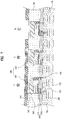
- FIG. 5 is a top view illustrating a light emitting device array of a display device according to an embodiment.
- FIG. 5 illustrates a structure in which the semiconductor light emitting devices 300 aligned in a row are connected to one first electrode 200 and one second electrode 400.
- this structure is illustrated for convenience of description of PM type semiconductor light emitting devices, and the present invention is not limited thereto.
- the semiconductor light emitting devices 300 having different internal resistances are electrically connected to the first electrode 200.
- the resistance with respect to each of the semiconductor light emitting devices 300 is a sum resistance of the line resistance of the first electrode 200 and the internal resistance of the semiconductor light emitting device 300.
- the line resistance of the first electrode 200 with respect to each of the semiconductor light emitting devices 300 connected to the first electrode 200 increases from one side of the current input direction of the first electrode 200 to the other side thereof. In other words, power loss occurs.
- the total resistance with respect to the semiconductor light emitting devices 300 may be uniformly controlled by reducing the distance between the n-type electrode and the p-type semiconductor layer 330 of each of the semiconductor light emitting devices 300 from one side of the current input direction of the first electrode 200 to the other side thereof.
- each of the semiconductor light emitting devices 300 may also be controlled by adjusting a thickness of layer or a chip size of each of the semiconductor light emitting devices 300 or a thickness or an area of the n-type electrode or the p-type electrode in addition to controlling the distance between the n-type electrode and the p-type semiconductor layer 330 of each of the semiconductor light emitting devices 300.
- FIG. 6 is a top view illustrating brightness variation before and after compensation of power loss of a light emitting device array.
- first electrodes and luminescent regions of a PM type light emitting device array are illustrated.
- the luminescent region corresponds to the p-type semiconductor layer of each of the semiconductor light emitting devices.
- Current is input to one ends of each of the first electrodes 200 indicated as two lines.
- the light emitting device array before compensation has a structure in which a plurality of semiconductor light emitting devices having the same brightness is aligned in a row.
- the semiconductor light emitting device is a horizontal semiconductor light emitting device, and each of the semiconductor light emitting devices has a uniform internal resistance.
- the distance between the n-type electrode and the p-type semiconductor layer is the same in each of the semiconductor light emitting devices.
- the light emitting device array after compensation has a structure in which the internal resistance of each of the semiconductor light emitting devices is designed to decrease from one side of the current input direction of the first electrode to the other side thereof. That is, the distance between the n-type electrode and the p-type semiconductor layer of each of the semiconductor light emitting devices decreases from one side of the current input direction of the first electrode to the other side thereof.
- a display device having minimized brightness variation may be fabricated by use of a light emitting device array having the same structure as described above, except that a plurality of semiconductor light emitting devices having the same brightness is used, and resistances of the semiconductor light emitting devices are adjusted.
- the display device includes a substrate, a plurality of first electrodes disposed on the substrate, a light emitting device array including a plurality of semiconductor light emitting devices electrically connected to the first electrodes and constituting individual pixels, a plurality of second electrodes electrically connected to the semiconductor light emitting devices, and a wavelength converting layer disposed on the semiconductor light emitting devices.
- the second electrodes may be electrically connected to the semiconductor light emitting devices via connection electrodes protruding from the second electrodes.
- a thickness or width of each of the connection electrodes may increase from one side of the current input direction of each the first electrodes to the other side thereof, or a length of each of the connection electrodes may decrease from one side of the current input direction of each the first electrodes to the other side thereof.
- a thickness or width of the first electrode may be designed to increase from one side of the current input direction of each the first electrodes to the other side thereof.
- the display device may emit light having uniform brightness by varying line resistance of the first electrode with respect to the semiconductor light emitting devices.
- FIG. 7 is a cross-sectional view partially illustrating a display device using semiconductor light emitting devices according to a second embodiment.
- the display device using semiconductor light emitting devices is a display device of PM type using semiconductor light emitting devices.
- the semiconductor light emitting device is a flip chip type light emitting device.
- the display device using the semiconductor light emitting devices includes a substrate 100, a plurality of first electrodes 200, an interlayer insulating layer 700, an anisotropic conductive film 800, a plurality of second electrodes 400, a light emitting device array including a plurality of semiconductor light emitting devices 300, and a wavelength converting layer 600.
- the substrate 100 may be a flexible substrate.
- the substrate 100 may be formed of a transparent material.
- the first electrodes 200 are disposed on the substrate 100.
- the interlayer insulating film 700 is disposed on the substrate 100 provided with the first electrodes 200.
- Auxiliary electrodes 220 are electrodes electrically connecting each of the first electrodes 200 with each of the semiconductor light emitting devices 300, disposed on the interlayer insulating film 700, and aligned to correspond to the first electrodes 200.
- the auxiliary electrodes 220 may be formed in dot shapes.
- the auxiliary electrodes 220 may be electrically connected to the first electrodes 200 via through-hole electrodes 210 that penetrate the interlayer insulating film 700.
- the second electrodes 400 are disposed on the interlayer insulating film 700 to be spaced apart from the auxiliary electrodes 220.
- the anisotropic conductive film 800 is disposed on the interlayer insulating film 700 on which the auxiliary electrodes 220 and the second electrodes 400 are disposed.
- An anisotropic conductive film is formed of a plurality of particles in which conductive cores are respectively coated with an insulating film.
- the insulating film When pressure or heat is applied to the anisotropic conductive film, the insulating film is destroyed at regions to which the pressure or heat is applied, such that the regions of the anisotropic conductive film are electrically connected to a layer via exposed cores of the anisotropic conductive film. In this case, the cores may be deformed to be connected to the layer.
- the semiconductor light emitting devices 300 are connected thereto in a flip chip form by applying heat or pressure thereto.
- the anisotropic conductive film 800 becomes conductive at conductive regions 801 between the p-type electrodes of the semiconductor light emitting devices 300 and the auxiliary electrodes 220 and between the n-type electrodes of the semiconductor light emitting device 300 and the second electrodes 400 to which heat or pressure is applied.
- anisotropic conductive film 800 is not conductive at nonconductive regions 802 to which heat or pressure is not applied.
- the anisotropic conductive film 800 may not only bond the semiconductor light emitting device 300 to the auxiliary electrode 220 but also electrically connect the semiconductor light emitting device 300 with the second electrode 400
- the light emitting device array includes a plurality of semiconductor light emitting devices 300 that constitute individual pixels and are electrically connected to the first electrodes 200.
- a plurality of first electrodes 200 may be disposed, and the semiconductor light emitting devices 300 may be aligned in plural rows.
- the semiconductor light emitting devices 300 in the same row may be electrically connected to one of the first electrodes 200.
- the semiconductor light emitting devices 300 are connected in a flip chip form, the semiconductor light emitting devices 300 grown on a transparent dielectric substrate 360 may be used.
- the semiconductor light emitting devices 300 may be nitride semiconductor light emitting devices. Due to excellent brightness, the semiconductor light emitting devices 300, which are small in size, may constitute individual sub-pixels.
- a barrier wall 500 may be disposed between the semiconductor light emitting devices 300.
- the wavelength converting layer 600 is disposed on the semiconductor light emitting devices 300.
- the semiconductor light emitting devices 300 are blue semiconductor light emitting devices emitting blue (B) light
- the wavelength converting layer 600 converting blue (B) into a color of an individual sub-pixel may be disposed.
- the wavelength converting layer 600 may include a red fluorescent (phosphor) material 601 and a green fluorescent (phosphor) material 602 constituting individual sub-pixels.
- the black matrix 610 may be disposed between the fluorescent (phosphor) materials in order to increase contrast ratio. That is, the black matrix 610 may improve contrast.
- a full color display in which the red (R), green (G), and blue (B) sub-pixels constitute one pixel may be designed by applying the red and green fluorescent (phosphor) materials to the blue semiconductor light emitting devices 300.
Landscapes
- Engineering & Computer Science (AREA)
- Physics & Mathematics (AREA)
- Computer Hardware Design (AREA)
- General Physics & Mathematics (AREA)
- Theoretical Computer Science (AREA)
- Led Devices (AREA)
- Led Device Packages (AREA)
- Devices For Indicating Variable Information By Combining Individual Elements (AREA)
Claims (11)
- Passive Matrixanzeigevorrichtung, die eine lichtemittierende Halbleitervorrichtung verwendet und Folgendes umfasst:ein Substrat (100);mehrere erste Elektroden (200), die auf dem Substrat (100) angeordnet sind;eine Anordnung lichtemittierender Vorrichtungen, die mehrere lichtemittierende Halbleitervorrichtungen (300) enthält, die mit den ersten Elektroden (200) elektrisch verbunden sind und einzelne Pixel bilden;mehrere zweite Elektroden (400), die mit den lichtemittierenden Halbleitervorrichtungen (300) verbunden sind; undeine Wellenlängenumsetzungsschicht (600), die auf den lichtemittierenden Halbleitervorrichtungen (300) angeordnet ist,dadurch gekennzeichnet, dass:jede der lichtemittierenden Halbleitervorrichtungen (300) eine horizontale Struktur besitzt und eine Halbleiterschicht (310) des n-Typs, eine aktive Schicht (320), die auf der Halbleiterschicht (310) des n-Typs angeordnet ist, eine Halbleiterschicht (330) des p-Typs, die auf der aktiven Schicht (320) angeordnet ist, eine Elektrode (340) des p-Typs und eine Elektrode (350) des n-Typs umfasst undein Abstand (m) zwischen der Elektrode (350) des n-Typs und der Halbleiterschicht (330) des p-Typs jeder der lichtemittierenden Halbleitervorrichtungen (300) von einer Seite einer Stromeingangsrichtung der ersten Elektrode (200) zu der anderen Seite hiervon abnimmt.
- Anzeigevorrichtung nach Anspruch 1, wobei die ersten Elektroden (200) und die zweiten Elektroden (400) jeweils so ausgerichtet sind, dass sie zueinander senkrecht sind.
- Anzeigevorrichtung nach Anspruch 1, wobei der Abstand (m) zwischen der Elektrode (350) des n-Typs und der Halbleiterschicht (330) des p-Typs der lichtemittierenden Halbleitervorrichtungen (300) von einer Seite der Stromeingangsrichtung der ersten Elektrode (200) zu der anderen Seite hiervon linear abnimmt.
- Anzeigevorrichtung nach Anspruch 1, wobei eine Differenz zwischen dem Abstand (m) einer ersten lichtemittierenden Halbleitervorrichtung der mehreren lichtemittierenden Halbleitervorrichtungen (300) und dem Abstand (m) einer zweiten lichtemittierenden Halbleitervorrichtung der mehreren lichtemittierenden Halbleitervorrichtungen (300), die sich in der Stromeingangsrichtung hinter der ersten lichtemittierenden Halbleitervorrichtung befindet, größer als ein Inkrement einer linearen Abnahme ist.
- Anzeigevorrichtung nach Anspruch 4, wobei die Halbleiterschichten (330) des p-Typs der lichtemittierenden Halbleitervorrichtungen (300) in der horizontalen Dichtung die gleiche Länge (L) besitzen.
- Anzeigevorrichtung nach Anspruch 1, wobei das Substrat (100) ein lichtdurchlässiges, biegsames Substrat ist.
- Anzeigevorrichtung nach Anspruch 1, wobei:die lichtemittierenden Halbleitervorrichtungen (300) blaues Licht emittierende Vorrichtungen sind; unddie Wellenlängenumsetzungsschicht (600) eine Umsetzungsschicht für gelbe Wellenlängen ist.
- Anzeigevorrichtung nach Anspruch 7, die ferner einen Farbfilter umfasst, der rote, grüne und blaue Farbfilter enthält, die auf der Umsetzungsschicht für gelbe Wellenlängen wiederholt ausgerichtet und angeordnet sind.
- Anzeigevorrichtung nach Anspruch 1, wobei:die lichtemittierenden Halbleitervorrichtungen (300) blaues Licht emittierende Vorrichtungen sind; unddie Wellenlängenumsetzungsschicht (600) ein rotes Fluoreszenzmaterial (Phosphormaterial), ein grünes Fluoreszenzmaterial (Phosphormaterial) und ein gelbes Fluoreszenzmaterial (Phosphormaterial), die einzelne Pixel bilden, enthält.
- Anzeigevorrichtung nach Anspruch 1, wobei die Wellenlängenumsetzungsschicht (600) ferner eine Schwarzmatrix enthält, die zwischen den Fluoreszenzmaterialien (Phosphormaterialien) angeordnet ist.
- Anzeigevorrichtung nach Anspruch 1, wobei rote, grüne und blaue Unterpixel ein Pixel bilden oder rote, grüne, blaue und weiße Unterpixel ein Pixel bilden.
Priority Applications (1)
| Application Number | Priority Date | Filing Date | Title |
|---|---|---|---|
| EP20203861.8A EP3789992B1 (de) | 2012-09-04 | 2013-06-05 | Anzeigevorrichtung mit verwendung von lichtemittierenden halbleiterbauelementen |
Applications Claiming Priority (2)
| Application Number | Priority Date | Filing Date | Title |
|---|---|---|---|
| KR20120097614A KR101422037B1 (ko) | 2012-09-04 | 2012-09-04 | 반도체 발광 소자를 이용한 디스플레이 장치 |
| PCT/KR2013/004965 WO2014038776A1 (en) | 2012-09-04 | 2013-06-05 | Display device using semiconductor light emitting device |
Related Child Applications (2)
| Application Number | Title | Priority Date | Filing Date |
|---|---|---|---|
| EP20203861.8A Division-Into EP3789992B1 (de) | 2012-09-04 | 2013-06-05 | Anzeigevorrichtung mit verwendung von lichtemittierenden halbleiterbauelementen |
| EP20203861.8A Division EP3789992B1 (de) | 2012-09-04 | 2013-06-05 | Anzeigevorrichtung mit verwendung von lichtemittierenden halbleiterbauelementen |
Publications (3)
| Publication Number | Publication Date |
|---|---|
| EP2893773A1 EP2893773A1 (de) | 2015-07-15 |
| EP2893773A4 EP2893773A4 (de) | 2016-05-11 |
| EP2893773B1 true EP2893773B1 (de) | 2020-12-09 |
Family
ID=50237357
Family Applications (2)
| Application Number | Title | Priority Date | Filing Date |
|---|---|---|---|
| EP20203861.8A Active EP3789992B1 (de) | 2012-09-04 | 2013-06-05 | Anzeigevorrichtung mit verwendung von lichtemittierenden halbleiterbauelementen |
| EP13835617.5A Active EP2893773B1 (de) | 2012-09-04 | 2013-06-05 | Anzeigevorrichtung mit lichtemittierendem halbleiterbauelement |
Family Applications Before (1)
| Application Number | Title | Priority Date | Filing Date |
|---|---|---|---|
| EP20203861.8A Active EP3789992B1 (de) | 2012-09-04 | 2013-06-05 | Anzeigevorrichtung mit verwendung von lichtemittierenden halbleiterbauelementen |
Country Status (4)
| Country | Link |
|---|---|
| US (1) | US9711692B2 (de) |
| EP (2) | EP3789992B1 (de) |
| KR (1) | KR101422037B1 (de) |
| WO (1) | WO2014038776A1 (de) |
Families Citing this family (36)
| Publication number | Priority date | Publication date | Assignee | Title |
|---|---|---|---|---|
| US10910350B2 (en) * | 2014-05-24 | 2021-02-02 | Hiphoton Co., Ltd. | Structure of a semiconductor array |
| KR101529934B1 (ko) * | 2014-07-01 | 2015-06-18 | 엘지전자 주식회사 | 반도체 발광 소자를 이용한 디스플레이 장치 |
| GB201420452D0 (en) | 2014-11-18 | 2014-12-31 | Mled Ltd | Integrated colour led micro-display |
| KR102322842B1 (ko) * | 2014-12-26 | 2021-11-08 | 엘지이노텍 주식회사 | 발광 소자 어레이 |
| US9721931B2 (en) | 2015-01-15 | 2017-08-01 | Industrial Technology Research Institute | Semiconductor light emitting device and fabricating method thereof |
| TWI572025B (zh) * | 2015-01-15 | 2017-02-21 | 財團法人工業技術研究院 | 半導體發光元件及其製作方法 |
| KR101688160B1 (ko) | 2015-01-27 | 2016-12-20 | 엘지전자 주식회사 | 반도체 발광 소자를 이용한 디스플레이 장치 및 이의 제조방법 |
| KR101688163B1 (ko) * | 2015-03-30 | 2016-12-20 | 엘지전자 주식회사 | 반도체 발광 소자를 이용한 디스플레이 장치 및 이의 제조방법 |
| KR102377794B1 (ko) * | 2015-07-06 | 2022-03-23 | 엘지전자 주식회사 | 반도체 발광 소자를 이용한 디스플레이 장치 및 이의 제조방법 |
| JP6612565B2 (ja) * | 2015-09-11 | 2019-11-27 | アルパッド株式会社 | ディスプレイパネル、表示装置およびディスプレイパネルの製造方法 |
| KR102407777B1 (ko) * | 2016-02-04 | 2022-06-10 | 에피스타 코포레이션 | 발광소자 및 그의 제조방법 |
| WO2017146477A1 (ko) * | 2016-02-26 | 2017-08-31 | 서울반도체주식회사 | 디스플레이 장치 및 그의 제조 방법 |
| KR102471687B1 (ko) * | 2016-02-26 | 2022-11-28 | 쑤저우 레킨 세미컨덕터 컴퍼니 리미티드 | 발광모듈 및 표시장치 |
| US9829710B1 (en) * | 2016-03-02 | 2017-11-28 | Valve Corporation | Display with stacked emission and control logic layers |
| US10332949B2 (en) * | 2016-07-06 | 2019-06-25 | Seoul Semiconductor Co., Ltd. | Display apparatus |
| CN106024844B (zh) * | 2016-07-27 | 2019-01-22 | 京东方科技集团股份有限公司 | 有机发光器件及其制备方法、显示装置 |
| KR102553630B1 (ko) | 2016-08-11 | 2023-07-10 | 삼성전자주식회사 | 발광소자 패키지 및 이를 이용한 디스플레이 장치 |
| TWI640109B (zh) * | 2016-08-11 | 2018-11-01 | 億光電子工業股份有限公司 | 顯示裝置 |
| CN109792817B (zh) * | 2016-09-22 | 2021-08-06 | Lg电子株式会社 | 使用半导体发光器件的显示装置及其制造方法 |
| CN110024142B (zh) * | 2016-11-24 | 2023-02-17 | Lg伊诺特有限公司 | 半导体器件和包括半导体器件的显示装置 |
| KR102019262B1 (ko) * | 2016-11-29 | 2019-11-04 | 고려대학교 산학협력단 | 발광 소자 디스플레이 장치 및 이의 제조 방법 |
| KR102555383B1 (ko) * | 2016-12-07 | 2023-07-12 | 엘지디스플레이 주식회사 | 유기발광소자를 이용한 조명장치 및 그 제조방법 |
| KR102781049B1 (ko) * | 2017-01-20 | 2025-03-18 | 엘지전자 주식회사 | 반도체 발광소자를 이용한 디스플레이 장치 |
| KR102507072B1 (ko) * | 2017-06-12 | 2023-03-07 | 엘지전자 주식회사 | 반도체 발광 소자를 이용한 디스플레이 장치 |
| KR102455483B1 (ko) * | 2017-06-30 | 2022-10-19 | 삼성전자주식회사 | Led 장치 및 그 제조 방법 |
| KR102565147B1 (ko) | 2017-11-08 | 2023-08-18 | 서울바이오시스 주식회사 | 복수의 픽셀들을 포함하는 디스플레이용 발광 다이오드 유닛 및 그것을 갖는 디스플레이 장치 |
| KR102421729B1 (ko) | 2017-12-14 | 2022-07-15 | 삼성전자주식회사 | 발광소자 패키지 및 이를 이용한 디스플레이 장치 |
| US11402075B2 (en) | 2018-01-03 | 2022-08-02 | Lg Electronics Inc. | Vehicle lamp using semiconductor light-emitting device |
| CN110112123A (zh) * | 2018-02-01 | 2019-08-09 | 晶元光电股份有限公司 | 发光装置及其制造方法 |
| FR3078442B1 (fr) * | 2018-02-26 | 2023-02-10 | Valeo Vision | Source lumineuse electroluminescente destinee a etre alimentee par une source de tension |
| KR102786764B1 (ko) * | 2018-07-11 | 2025-03-27 | 엘지전자 주식회사 | 반도체 발광 소자를 이용한 디스플레이 장치 및 이의 제조방법 |
| US11621253B2 (en) * | 2018-11-02 | 2023-04-04 | Seoul Viosys Co., Ltd. | Light emitting device |
| KR102694326B1 (ko) | 2019-10-11 | 2024-08-13 | 삼성전자주식회사 | 디스플레이 모듈 및 이의 제조 방법 |
| CN116246547A (zh) | 2020-12-02 | 2023-06-09 | 湖北长江新型显示产业创新中心有限公司 | 显示面板和显示装置 |
| CN119092503B (zh) * | 2023-06-06 | 2026-02-10 | 京东方科技集团股份有限公司 | 发光组件、显示面板及发光组件的制备方法 |
| CN118888672B (zh) * | 2024-10-08 | 2025-01-28 | 江西卓讯微电子有限公司 | 一种晶膜屏及其制备方法 |
Family Cites Families (24)
| Publication number | Priority date | Publication date | Assignee | Title |
|---|---|---|---|---|
| JPH11260560A (ja) * | 1998-03-06 | 1999-09-24 | Denso Corp | El素子 |
| US20060152150A1 (en) | 2002-10-01 | 2006-07-13 | Herbert Boerner | Electroluminescent display with improved light outcoupling |
| KR20040060337A (ko) * | 2002-12-30 | 2004-07-06 | 엘지전자 주식회사 | 플라즈마 디스플레이 패널 |
| EP2509397B1 (de) * | 2003-09-19 | 2018-12-05 | Sony Corporation | Anzeigeeinheit mit Resonatorstruktur |
| JP2005158369A (ja) * | 2003-11-21 | 2005-06-16 | Toyota Industries Corp | 光学部材及び照明装置 |
| TWI251188B (en) * | 2004-03-31 | 2006-03-11 | Fuji Photo Film Co Ltd | Passive matrix light emitting device |
| KR100631521B1 (ko) * | 2004-04-17 | 2006-10-11 | 엘지전자 주식회사 | 발광 장치 와 그의 제조방법 |
| US7868856B2 (en) * | 2004-08-20 | 2011-01-11 | Koninklijke Philips Electronics N.V. | Data signal driver for light emitting display |
| KR100656496B1 (ko) * | 2004-09-21 | 2006-12-11 | 삼성에스디아이 주식회사 | 풀 칼라 유기 전계 발광 표시 소자 및 그 제조방법 |
| WO2006050372A2 (en) * | 2004-11-01 | 2006-05-11 | The Regents Of The University Of California | Interdigitated multi-pixel arrays for the fabrication of light-emitting devices with very low series-resistances and improved heat-sinking |
| KR100773939B1 (ko) * | 2005-02-16 | 2007-11-07 | 주식회사 대우일렉트로닉스 | 유기 전계 발광 소자 |
| TWI268739B (en) * | 2005-06-21 | 2006-12-11 | Au Optronics Corp | Organic electroluminescent device |
| KR100759561B1 (ko) * | 2005-11-30 | 2007-09-18 | 삼성에스디아이 주식회사 | 플라즈마 디스플레이 패널 |
| KR100784015B1 (ko) * | 2006-12-13 | 2007-12-07 | 삼성에스디아이 주식회사 | 유기전계발광 표시장치 |
| JP4718504B2 (ja) * | 2007-03-07 | 2011-07-06 | 株式会社沖データ | 表示装置 |
| JP5167723B2 (ja) * | 2007-08-21 | 2013-03-21 | セイコーエプソン株式会社 | 発光装置 |
| KR100986359B1 (ko) | 2008-03-14 | 2010-10-08 | 엘지이노텍 주식회사 | 발광 장치 및 이를 구비한 표시 장치 |
| TWI464921B (zh) * | 2009-02-25 | 2014-12-11 | 晶元光電股份有限公司 | 主波長分佈收斂之發光元件及其製造方法 |
| KR101649224B1 (ko) * | 2008-12-16 | 2016-08-18 | 엘지디스플레이 주식회사 | 백색 전면발광 유기전계발광 표시장치 |
| JP2010267481A (ja) | 2009-05-14 | 2010-11-25 | Hitachi Displays Ltd | バックライト装置および表示装置 |
| US20110012147A1 (en) * | 2009-07-15 | 2011-01-20 | Koninklijke Philips Electronics N.V. | Wavelength-converted semiconductor light emitting device including a filter and a scattering structure |
| JP2011216668A (ja) * | 2010-03-31 | 2011-10-27 | Sony Corp | 発光装置 |
| WO2012032661A1 (ja) * | 2010-09-11 | 2012-03-15 | パイオニア株式会社 | 有機elパネル |
| CN103299714B (zh) * | 2010-12-28 | 2016-01-20 | 夏普株式会社 | 有机el显示单元、有机el显示装置和有机el显示单元的制造方法 |
-
2012
- 2012-09-04 KR KR20120097614A patent/KR101422037B1/ko not_active Expired - Fee Related
-
2013
- 2013-06-05 WO PCT/KR2013/004965 patent/WO2014038776A1/en not_active Ceased
- 2013-06-05 EP EP20203861.8A patent/EP3789992B1/de active Active
- 2013-06-05 EP EP13835617.5A patent/EP2893773B1/de active Active
- 2013-06-05 US US14/425,587 patent/US9711692B2/en active Active
Non-Patent Citations (1)
| Title |
|---|
| None * |
Also Published As
| Publication number | Publication date |
|---|---|
| EP2893773A4 (de) | 2016-05-11 |
| WO2014038776A1 (en) | 2014-03-13 |
| US20150228865A1 (en) | 2015-08-13 |
| EP2893773A1 (de) | 2015-07-15 |
| US9711692B2 (en) | 2017-07-18 |
| EP3789992A1 (de) | 2021-03-10 |
| KR20140030887A (ko) | 2014-03-12 |
| EP3789992B1 (de) | 2023-05-10 |
| KR101422037B1 (ko) | 2014-07-23 |
Similar Documents
| Publication | Publication Date | Title |
|---|---|---|
| US9711692B2 (en) | Display device using semiconductor light emitting devices having different structures | |
| US12155024B2 (en) | Display apparatus and manufacturing method thereof | |
| US9391051B2 (en) | Display device using semiconductor light emitting device and method of fabricating the same | |
| US11985856B2 (en) | Display apparatus | |
| US12009385B2 (en) | Light-emitting diode unit for display comprising plurality of pixels and display device having same | |
| EP3439042B1 (de) | Anzeigevorrichtung und herstellungsverfahren dafür | |
| US10096647B2 (en) | Display apparatus having a plurality of reflective electrodes | |
| US20220320057A1 (en) | Display device using micro led and method for manufacturing same | |
| US10380930B2 (en) | Heterogeneous light emitter display system | |
| US20220367774A1 (en) | Display device using micro led, and manufacturing method therefor | |
| US20180166470A1 (en) | Display apparatus and connecting method of light emitting part thereof | |
| US12232392B2 (en) | Display apparatus using inorganic light-emitting diode | |
| KR20180118090A (ko) | 마이크로 led 디스플레이 화소 조립체 및 이의 제조방법 | |
| KR20190097946A (ko) | 반도체 발광소자를 이용한 디스플레이 장치의 제조방법 | |
| CN112567522B (zh) | 使用半导体发光二极管的显示装置及其制造方法 | |
| KR20220043742A (ko) | 마이크로 led 및 이를 구비한 디스플레이 모듈 | |
| CN120167148A (zh) | 半导体发光器件、包括半导体发光器件的显示装置及其制造方法 |
Legal Events
| Date | Code | Title | Description |
|---|---|---|---|
| PUAI | Public reference made under article 153(3) epc to a published international application that has entered the european phase |
Free format text: ORIGINAL CODE: 0009012 |
|
| 17P | Request for examination filed |
Effective date: 20150213 |
|
| AK | Designated contracting states |
Kind code of ref document: A1 Designated state(s): AL AT BE BG CH CY CZ DE DK EE ES FI FR GB GR HR HU IE IS IT LI LT LU LV MC MK MT NL NO PL PT RO RS SE SI SK SM TR |
|
| AX | Request for extension of the european patent |
Extension state: BA ME |
|
| DAX | Request for extension of the european patent (deleted) | ||
| RA4 | Supplementary search report drawn up and despatched (corrected) |
Effective date: 20160413 |
|
| RIC1 | Information provided on ipc code assigned before grant |
Ipc: H05B 33/02 20060101AFI20160407BHEP |
|
| STAA | Information on the status of an ep patent application or granted ep patent |
Free format text: STATUS: EXAMINATION IS IN PROGRESS |
|
| 17Q | First examination report despatched |
Effective date: 20181026 |
|
| GRAP | Despatch of communication of intention to grant a patent |
Free format text: ORIGINAL CODE: EPIDOSNIGR1 |
|
| STAA | Information on the status of an ep patent application or granted ep patent |
Free format text: STATUS: GRANT OF PATENT IS INTENDED |
|
| INTG | Intention to grant announced |
Effective date: 20200622 |
|
| RAP1 | Party data changed (applicant data changed or rights of an application transferred) |
Owner name: LG ELECTRONICS INC. |
|
| GRAS | Grant fee paid |
Free format text: ORIGINAL CODE: EPIDOSNIGR3 |
|
| GRAA | (expected) grant |
Free format text: ORIGINAL CODE: 0009210 |
|
| STAA | Information on the status of an ep patent application or granted ep patent |
Free format text: STATUS: THE PATENT HAS BEEN GRANTED |
|
| AK | Designated contracting states |
Kind code of ref document: B1 Designated state(s): AL AT BE BG CH CY CZ DE DK EE ES FI FR GB GR HR HU IE IS IT LI LT LU LV MC MK MT NL NO PL PT RO RS SE SI SK SM TR |
|
| REG | Reference to a national code |
Ref country code: GB Ref legal event code: FG4D |
|
| REG | Reference to a national code |
Ref country code: AT Ref legal event code: REF Ref document number: 1344682 Country of ref document: AT Kind code of ref document: T Effective date: 20201215 Ref country code: CH Ref legal event code: EP |
|
| REG | Reference to a national code |
Ref country code: DE Ref legal event code: R096 Ref document number: 602013074670 Country of ref document: DE |
|
| REG | Reference to a national code |
Ref country code: IE Ref legal event code: FG4D |
|
| PG25 | Lapsed in a contracting state [announced via postgrant information from national office to epo] |
Ref country code: GR Free format text: LAPSE BECAUSE OF FAILURE TO SUBMIT A TRANSLATION OF THE DESCRIPTION OR TO PAY THE FEE WITHIN THE PRESCRIBED TIME-LIMIT Effective date: 20210310 Ref country code: FI Free format text: LAPSE BECAUSE OF FAILURE TO SUBMIT A TRANSLATION OF THE DESCRIPTION OR TO PAY THE FEE WITHIN THE PRESCRIBED TIME-LIMIT Effective date: 20201209 Ref country code: RS Free format text: LAPSE BECAUSE OF FAILURE TO SUBMIT A TRANSLATION OF THE DESCRIPTION OR TO PAY THE FEE WITHIN THE PRESCRIBED TIME-LIMIT Effective date: 20201209 Ref country code: NO Free format text: LAPSE BECAUSE OF FAILURE TO SUBMIT A TRANSLATION OF THE DESCRIPTION OR TO PAY THE FEE WITHIN THE PRESCRIBED TIME-LIMIT Effective date: 20210309 |
|
| REG | Reference to a national code |
Ref country code: AT Ref legal event code: MK05 Ref document number: 1344682 Country of ref document: AT Kind code of ref document: T Effective date: 20201209 |
|
| PG25 | Lapsed in a contracting state [announced via postgrant information from national office to epo] |
Ref country code: BG Free format text: LAPSE BECAUSE OF FAILURE TO SUBMIT A TRANSLATION OF THE DESCRIPTION OR TO PAY THE FEE WITHIN THE PRESCRIBED TIME-LIMIT Effective date: 20210309 Ref country code: SE Free format text: LAPSE BECAUSE OF FAILURE TO SUBMIT A TRANSLATION OF THE DESCRIPTION OR TO PAY THE FEE WITHIN THE PRESCRIBED TIME-LIMIT Effective date: 20201209 Ref country code: LV Free format text: LAPSE BECAUSE OF FAILURE TO SUBMIT A TRANSLATION OF THE DESCRIPTION OR TO PAY THE FEE WITHIN THE PRESCRIBED TIME-LIMIT Effective date: 20201209 |
|
| REG | Reference to a national code |
Ref country code: NL Ref legal event code: MP Effective date: 20201209 |
|
| PG25 | Lapsed in a contracting state [announced via postgrant information from national office to epo] |
Ref country code: HR Free format text: LAPSE BECAUSE OF FAILURE TO SUBMIT A TRANSLATION OF THE DESCRIPTION OR TO PAY THE FEE WITHIN THE PRESCRIBED TIME-LIMIT Effective date: 20201209 Ref country code: NL Free format text: LAPSE BECAUSE OF FAILURE TO SUBMIT A TRANSLATION OF THE DESCRIPTION OR TO PAY THE FEE WITHIN THE PRESCRIBED TIME-LIMIT Effective date: 20201209 |
|
| REG | Reference to a national code |
Ref country code: LT Ref legal event code: MG9D |
|
| PG25 | Lapsed in a contracting state [announced via postgrant information from national office to epo] |
Ref country code: EE Free format text: LAPSE BECAUSE OF FAILURE TO SUBMIT A TRANSLATION OF THE DESCRIPTION OR TO PAY THE FEE WITHIN THE PRESCRIBED TIME-LIMIT Effective date: 20201209 Ref country code: CZ Free format text: LAPSE BECAUSE OF FAILURE TO SUBMIT A TRANSLATION OF THE DESCRIPTION OR TO PAY THE FEE WITHIN THE PRESCRIBED TIME-LIMIT Effective date: 20201209 Ref country code: SM Free format text: LAPSE BECAUSE OF FAILURE TO SUBMIT A TRANSLATION OF THE DESCRIPTION OR TO PAY THE FEE WITHIN THE PRESCRIBED TIME-LIMIT Effective date: 20201209 Ref country code: SK Free format text: LAPSE BECAUSE OF FAILURE TO SUBMIT A TRANSLATION OF THE DESCRIPTION OR TO PAY THE FEE WITHIN THE PRESCRIBED TIME-LIMIT Effective date: 20201209 Ref country code: PT Free format text: LAPSE BECAUSE OF FAILURE TO SUBMIT A TRANSLATION OF THE DESCRIPTION OR TO PAY THE FEE WITHIN THE PRESCRIBED TIME-LIMIT Effective date: 20210409 Ref country code: RO Free format text: LAPSE BECAUSE OF FAILURE TO SUBMIT A TRANSLATION OF THE DESCRIPTION OR TO PAY THE FEE WITHIN THE PRESCRIBED TIME-LIMIT Effective date: 20201209 Ref country code: LT Free format text: LAPSE BECAUSE OF FAILURE TO SUBMIT A TRANSLATION OF THE DESCRIPTION OR TO PAY THE FEE WITHIN THE PRESCRIBED TIME-LIMIT Effective date: 20201209 |
|
| PG25 | Lapsed in a contracting state [announced via postgrant information from national office to epo] |
Ref country code: PL Free format text: LAPSE BECAUSE OF FAILURE TO SUBMIT A TRANSLATION OF THE DESCRIPTION OR TO PAY THE FEE WITHIN THE PRESCRIBED TIME-LIMIT Effective date: 20201209 Ref country code: AT Free format text: LAPSE BECAUSE OF FAILURE TO SUBMIT A TRANSLATION OF THE DESCRIPTION OR TO PAY THE FEE WITHIN THE PRESCRIBED TIME-LIMIT Effective date: 20201209 |
|
| REG | Reference to a national code |
Ref country code: DE Ref legal event code: R097 Ref document number: 602013074670 Country of ref document: DE |
|
| PG25 | Lapsed in a contracting state [announced via postgrant information from national office to epo] |
Ref country code: IS Free format text: LAPSE BECAUSE OF FAILURE TO SUBMIT A TRANSLATION OF THE DESCRIPTION OR TO PAY THE FEE WITHIN THE PRESCRIBED TIME-LIMIT Effective date: 20210409 |
|
| PLBE | No opposition filed within time limit |
Free format text: ORIGINAL CODE: 0009261 |
|
| STAA | Information on the status of an ep patent application or granted ep patent |
Free format text: STATUS: NO OPPOSITION FILED WITHIN TIME LIMIT |
|
| PG25 | Lapsed in a contracting state [announced via postgrant information from national office to epo] |
Ref country code: IT Free format text: LAPSE BECAUSE OF FAILURE TO SUBMIT A TRANSLATION OF THE DESCRIPTION OR TO PAY THE FEE WITHIN THE PRESCRIBED TIME-LIMIT Effective date: 20201209 Ref country code: AL Free format text: LAPSE BECAUSE OF FAILURE TO SUBMIT A TRANSLATION OF THE DESCRIPTION OR TO PAY THE FEE WITHIN THE PRESCRIBED TIME-LIMIT Effective date: 20201209 |
|
| 26N | No opposition filed |
Effective date: 20210910 |
|
| PG25 | Lapsed in a contracting state [announced via postgrant information from national office to epo] |
Ref country code: ES Free format text: LAPSE BECAUSE OF FAILURE TO SUBMIT A TRANSLATION OF THE DESCRIPTION OR TO PAY THE FEE WITHIN THE PRESCRIBED TIME-LIMIT Effective date: 20201209 Ref country code: DK Free format text: LAPSE BECAUSE OF FAILURE TO SUBMIT A TRANSLATION OF THE DESCRIPTION OR TO PAY THE FEE WITHIN THE PRESCRIBED TIME-LIMIT Effective date: 20201209 Ref country code: SI Free format text: LAPSE BECAUSE OF FAILURE TO SUBMIT A TRANSLATION OF THE DESCRIPTION OR TO PAY THE FEE WITHIN THE PRESCRIBED TIME-LIMIT Effective date: 20201209 |
|
| PG25 | Lapsed in a contracting state [announced via postgrant information from national office to epo] |
Ref country code: MC Free format text: LAPSE BECAUSE OF FAILURE TO SUBMIT A TRANSLATION OF THE DESCRIPTION OR TO PAY THE FEE WITHIN THE PRESCRIBED TIME-LIMIT Effective date: 20201209 |
|
| REG | Reference to a national code |
Ref country code: CH Ref legal event code: PL |
|
| GBPC | Gb: european patent ceased through non-payment of renewal fee |
Effective date: 20210605 |
|
| REG | Reference to a national code |
Ref country code: BE Ref legal event code: MM Effective date: 20210630 |
|
| PG25 | Lapsed in a contracting state [announced via postgrant information from national office to epo] |
Ref country code: LU Free format text: LAPSE BECAUSE OF NON-PAYMENT OF DUE FEES Effective date: 20210605 |
|
| PG25 | Lapsed in a contracting state [announced via postgrant information from national office to epo] |
Ref country code: LI Free format text: LAPSE BECAUSE OF NON-PAYMENT OF DUE FEES Effective date: 20210630 Ref country code: IE Free format text: LAPSE BECAUSE OF NON-PAYMENT OF DUE FEES Effective date: 20210605 Ref country code: GB Free format text: LAPSE BECAUSE OF NON-PAYMENT OF DUE FEES Effective date: 20210605 Ref country code: CH Free format text: LAPSE BECAUSE OF NON-PAYMENT OF DUE FEES Effective date: 20210630 |
|
| PG25 | Lapsed in a contracting state [announced via postgrant information from national office to epo] |
Ref country code: IS Free format text: LAPSE BECAUSE OF FAILURE TO SUBMIT A TRANSLATION OF THE DESCRIPTION OR TO PAY THE FEE WITHIN THE PRESCRIBED TIME-LIMIT Effective date: 20210409 Ref country code: FR Free format text: LAPSE BECAUSE OF NON-PAYMENT OF DUE FEES Effective date: 20210630 |
|
| PG25 | Lapsed in a contracting state [announced via postgrant information from national office to epo] |
Ref country code: BE Free format text: LAPSE BECAUSE OF NON-PAYMENT OF DUE FEES Effective date: 20210630 |
|
| PG25 | Lapsed in a contracting state [announced via postgrant information from national office to epo] |
Ref country code: HU Free format text: LAPSE BECAUSE OF FAILURE TO SUBMIT A TRANSLATION OF THE DESCRIPTION OR TO PAY THE FEE WITHIN THE PRESCRIBED TIME-LIMIT; INVALID AB INITIO Effective date: 20130605 |
|
| PG25 | Lapsed in a contracting state [announced via postgrant information from national office to epo] |
Ref country code: CY Free format text: LAPSE BECAUSE OF FAILURE TO SUBMIT A TRANSLATION OF THE DESCRIPTION OR TO PAY THE FEE WITHIN THE PRESCRIBED TIME-LIMIT Effective date: 20201209 |
|
| PG25 | Lapsed in a contracting state [announced via postgrant information from national office to epo] |
Ref country code: MK Free format text: LAPSE BECAUSE OF FAILURE TO SUBMIT A TRANSLATION OF THE DESCRIPTION OR TO PAY THE FEE WITHIN THE PRESCRIBED TIME-LIMIT Effective date: 20201209 |
|
| PG25 | Lapsed in a contracting state [announced via postgrant information from national office to epo] |
Ref country code: TR Free format text: LAPSE BECAUSE OF FAILURE TO SUBMIT A TRANSLATION OF THE DESCRIPTION OR TO PAY THE FEE WITHIN THE PRESCRIBED TIME-LIMIT Effective date: 20201209 |
|
| PG25 | Lapsed in a contracting state [announced via postgrant information from national office to epo] |
Ref country code: MT Free format text: LAPSE BECAUSE OF FAILURE TO SUBMIT A TRANSLATION OF THE DESCRIPTION OR TO PAY THE FEE WITHIN THE PRESCRIBED TIME-LIMIT Effective date: 20201209 |
|
| PGFP | Annual fee paid to national office [announced via postgrant information from national office to epo] |
Ref country code: DE Payment date: 20250508 Year of fee payment: 13 |