EP2879166B1 - Plasma processing method - Google Patents
Plasma processing method Download PDFInfo
- Publication number
- EP2879166B1 EP2879166B1 EP13833486.7A EP13833486A EP2879166B1 EP 2879166 B1 EP2879166 B1 EP 2879166B1 EP 13833486 A EP13833486 A EP 13833486A EP 2879166 B1 EP2879166 B1 EP 2879166B1
- Authority
- EP
- European Patent Office
- Prior art keywords
- gas
- plasma
- plasma processing
- containing material
- titanium
- Prior art date
- Legal status (The legal status is an assumption and is not a legal conclusion. Google has not performed a legal analysis and makes no representation as to the accuracy of the status listed.)
- Active
Links
- 238000003672 processing method Methods 0.000 title claims description 29
- 239000007789 gas Substances 0.000 claims description 307
- 238000000034 method Methods 0.000 claims description 211
- 238000012545 processing Methods 0.000 claims description 197
- 239000000463 material Substances 0.000 claims description 146
- 239000010936 titanium Substances 0.000 claims description 111
- RTAQQCXQSZGOHL-UHFFFAOYSA-N Titanium Chemical compound [Ti] RTAQQCXQSZGOHL-UHFFFAOYSA-N 0.000 claims description 103
- 229910052719 titanium Inorganic materials 0.000 claims description 103
- 238000005530 etching Methods 0.000 claims description 84
- 229910052731 fluorine Inorganic materials 0.000 claims description 83
- YCKRFDGAMUMZLT-UHFFFAOYSA-N Fluorine atom Chemical compound [F] YCKRFDGAMUMZLT-UHFFFAOYSA-N 0.000 claims description 82
- 239000011737 fluorine Substances 0.000 claims description 82
- 229910052799 carbon Inorganic materials 0.000 claims description 45
- OKTJSMMVPCPJKN-UHFFFAOYSA-N Carbon Chemical compound [C] OKTJSMMVPCPJKN-UHFFFAOYSA-N 0.000 claims description 44
- QJGQUHMNIGDVPM-UHFFFAOYSA-N nitrogen group Chemical group [N] QJGQUHMNIGDVPM-UHFFFAOYSA-N 0.000 claims description 41
- ATJFFYVFTNAWJD-UHFFFAOYSA-N Tin Chemical compound [Sn] ATJFFYVFTNAWJD-UHFFFAOYSA-N 0.000 claims description 20
- 239000000758 substrate Substances 0.000 claims description 18
- XPDWGBQVDMORPB-UHFFFAOYSA-N Fluoroform Chemical compound FC(F)F XPDWGBQVDMORPB-UHFFFAOYSA-N 0.000 claims description 17
- 235000012431 wafers Nutrition 0.000 description 94
- 239000010408 film Substances 0.000 description 71
- 238000010586 diagram Methods 0.000 description 21
- 229910052718 tin Inorganic materials 0.000 description 20
- 238000005108 dry cleaning Methods 0.000 description 15
- 230000002093 peripheral effect Effects 0.000 description 10
- 230000000694 effects Effects 0.000 description 9
- 238000009792 diffusion process Methods 0.000 description 8
- 238000002474 experimental method Methods 0.000 description 8
- 239000002826 coolant Substances 0.000 description 4
- 230000009977 dual effect Effects 0.000 description 4
- -1 e.g. Substances 0.000 description 4
- 238000003860 storage Methods 0.000 description 3
- IJGRMHOSHXDMSA-UHFFFAOYSA-N Atomic nitrogen Chemical compound N#N IJGRMHOSHXDMSA-UHFFFAOYSA-N 0.000 description 2
- 229910010342 TiF4 Inorganic materials 0.000 description 2
- GWEVSGVZZGPLCZ-UHFFFAOYSA-N Titan oxide Chemical compound O=[Ti]=O GWEVSGVZZGPLCZ-UHFFFAOYSA-N 0.000 description 2
- 229910052782 aluminium Inorganic materials 0.000 description 2
- XAGFODPZIPBFFR-UHFFFAOYSA-N aluminium Chemical compound [Al] XAGFODPZIPBFFR-UHFFFAOYSA-N 0.000 description 2
- 239000004020 conductor Substances 0.000 description 2
- 230000001186 cumulative effect Effects 0.000 description 2
- 150000002500 ions Chemical class 0.000 description 2
- 238000005192 partition Methods 0.000 description 2
- 239000004065 semiconductor Substances 0.000 description 2
- 229910052710 silicon Inorganic materials 0.000 description 2
- 239000010703 silicon Substances 0.000 description 2
- VYPSYNLAJGMNEJ-UHFFFAOYSA-N silicon dioxide Inorganic materials O=[Si]=O VYPSYNLAJGMNEJ-UHFFFAOYSA-N 0.000 description 2
- 239000010409 thin film Substances 0.000 description 2
- XROWMBWRMNHXMF-UHFFFAOYSA-J titanium tetrafluoride Chemical compound [F-].[F-].[F-].[F-].[Ti+4] XROWMBWRMNHXMF-UHFFFAOYSA-J 0.000 description 2
- 238000012546 transfer Methods 0.000 description 2
- QVGXLLKOCUKJST-UHFFFAOYSA-N atomic oxygen Chemical compound [O] QVGXLLKOCUKJST-UHFFFAOYSA-N 0.000 description 1
- 230000015556 catabolic process Effects 0.000 description 1
- 238000006243 chemical reaction Methods 0.000 description 1
- 238000005229 chemical vapour deposition Methods 0.000 description 1
- 238000006731 degradation reaction Methods 0.000 description 1
- 230000000593 degrading effect Effects 0.000 description 1
- 238000000151 deposition Methods 0.000 description 1
- 238000005137 deposition process Methods 0.000 description 1
- 239000001307 helium Substances 0.000 description 1
- 229910052734 helium Inorganic materials 0.000 description 1
- SWQJXJOGLNCZEY-UHFFFAOYSA-N helium atom Chemical compound [He] SWQJXJOGLNCZEY-UHFFFAOYSA-N 0.000 description 1
- 229910052739 hydrogen Inorganic materials 0.000 description 1
- 239000011229 interlayer Substances 0.000 description 1
- 238000004519 manufacturing process Methods 0.000 description 1
- 238000005259 measurement Methods 0.000 description 1
- 229910052751 metal Inorganic materials 0.000 description 1
- 239000002184 metal Substances 0.000 description 1
- 229910052757 nitrogen Inorganic materials 0.000 description 1
- 239000001301 oxygen Substances 0.000 description 1
- 229910052760 oxygen Inorganic materials 0.000 description 1
- 238000005268 plasma chemical vapour deposition Methods 0.000 description 1
- 238000001020 plasma etching Methods 0.000 description 1
- 239000010453 quartz Substances 0.000 description 1
- 229910052814 silicon oxide Inorganic materials 0.000 description 1
Images


Classifications
-
- H—ELECTRICITY
- H01—ELECTRIC ELEMENTS
- H01J—ELECTRIC DISCHARGE TUBES OR DISCHARGE LAMPS
- H01J37/00—Discharge tubes with provision for introducing objects or material to be exposed to the discharge, e.g. for the purpose of examination or processing thereof
- H01J37/32—Gas-filled discharge tubes
- H01J37/32431—Constructional details of the reactor
- H01J37/3244—Gas supply means
-
- C—CHEMISTRY; METALLURGY
- C23—COATING METALLIC MATERIAL; COATING MATERIAL WITH METALLIC MATERIAL; CHEMICAL SURFACE TREATMENT; DIFFUSION TREATMENT OF METALLIC MATERIAL; COATING BY VACUUM EVAPORATION, BY SPUTTERING, BY ION IMPLANTATION OR BY CHEMICAL VAPOUR DEPOSITION, IN GENERAL; INHIBITING CORROSION OF METALLIC MATERIAL OR INCRUSTATION IN GENERAL
- C23F—NON-MECHANICAL REMOVAL OF METALLIC MATERIAL FROM SURFACE; INHIBITING CORROSION OF METALLIC MATERIAL OR INCRUSTATION IN GENERAL; MULTI-STEP PROCESSES FOR SURFACE TREATMENT OF METALLIC MATERIAL INVOLVING AT LEAST ONE PROCESS PROVIDED FOR IN CLASS C23 AND AT LEAST ONE PROCESS COVERED BY SUBCLASS C21D OR C22F OR CLASS C25
- C23F4/00—Processes for removing metallic material from surfaces, not provided for in group C23F1/00 or C23F3/00
-
- H—ELECTRICITY
- H01—ELECTRIC ELEMENTS
- H01J—ELECTRIC DISCHARGE TUBES OR DISCHARGE LAMPS
- H01J37/00—Discharge tubes with provision for introducing objects or material to be exposed to the discharge, e.g. for the purpose of examination or processing thereof
- H01J37/32—Gas-filled discharge tubes
- H01J37/32009—Arrangements for generation of plasma specially adapted for examination or treatment of objects, e.g. plasma sources
- H01J37/32082—Radio frequency generated discharge
- H01J37/32091—Radio frequency generated discharge the radio frequency energy being capacitively coupled to the plasma
-
- H—ELECTRICITY
- H01—ELECTRIC ELEMENTS
- H01J—ELECTRIC DISCHARGE TUBES OR DISCHARGE LAMPS
- H01J37/00—Discharge tubes with provision for introducing objects or material to be exposed to the discharge, e.g. for the purpose of examination or processing thereof
- H01J37/32—Gas-filled discharge tubes
- H01J37/32009—Arrangements for generation of plasma specially adapted for examination or treatment of objects, e.g. plasma sources
- H01J37/32082—Radio frequency generated discharge
- H01J37/32137—Radio frequency generated discharge controlling of the discharge by modulation of energy
- H01J37/32155—Frequency modulation
- H01J37/32165—Plural frequencies
-
- H—ELECTRICITY
- H01—ELECTRIC ELEMENTS
- H01J—ELECTRIC DISCHARGE TUBES OR DISCHARGE LAMPS
- H01J37/00—Discharge tubes with provision for introducing objects or material to be exposed to the discharge, e.g. for the purpose of examination or processing thereof
- H01J37/32—Gas-filled discharge tubes
- H01J37/32431—Constructional details of the reactor
- H01J37/3244—Gas supply means
- H01J37/32449—Gas control, e.g. control of the gas flow
-
- H—ELECTRICITY
- H01—ELECTRIC ELEMENTS
- H01J—ELECTRIC DISCHARGE TUBES OR DISCHARGE LAMPS
- H01J37/00—Discharge tubes with provision for introducing objects or material to be exposed to the discharge, e.g. for the purpose of examination or processing thereof
- H01J37/32—Gas-filled discharge tubes
- H01J37/32431—Constructional details of the reactor
- H01J37/32458—Vessel
-
- H—ELECTRICITY
- H01—ELECTRIC ELEMENTS
- H01J—ELECTRIC DISCHARGE TUBES OR DISCHARGE LAMPS
- H01J37/00—Discharge tubes with provision for introducing objects or material to be exposed to the discharge, e.g. for the purpose of examination or processing thereof
- H01J37/32—Gas-filled discharge tubes
- H01J37/32431—Constructional details of the reactor
- H01J37/32798—Further details of plasma apparatus not provided for in groups H01J37/3244 - H01J37/32788; special provisions for cleaning or maintenance of the apparatus
- H01J37/32853—Hygiene
- H01J37/32862—In situ cleaning of vessels and/or internal parts
-
- H—ELECTRICITY
- H01—ELECTRIC ELEMENTS
- H01L—SEMICONDUCTOR DEVICES NOT COVERED BY CLASS H10
- H01L21/00—Processes or apparatus adapted for the manufacture or treatment of semiconductor or solid state devices or of parts thereof
- H01L21/02—Manufacture or treatment of semiconductor devices or of parts thereof
- H01L21/04—Manufacture or treatment of semiconductor devices or of parts thereof the devices having potential barriers, e.g. a PN junction, depletion layer or carrier concentration layer
- H01L21/18—Manufacture or treatment of semiconductor devices or of parts thereof the devices having potential barriers, e.g. a PN junction, depletion layer or carrier concentration layer the devices having semiconductor bodies comprising elements of Group IV of the Periodic Table or AIIIBV compounds with or without impurities, e.g. doping materials
- H01L21/30—Treatment of semiconductor bodies using processes or apparatus not provided for in groups H01L21/20 - H01L21/26
- H01L21/31—Treatment of semiconductor bodies using processes or apparatus not provided for in groups H01L21/20 - H01L21/26 to form insulating layers thereon, e.g. for masking or by using photolithographic techniques; After treatment of these layers; Selection of materials for these layers
- H01L21/3105—After-treatment
- H01L21/311—Etching the insulating layers by chemical or physical means
- H01L21/31105—Etching inorganic layers
- H01L21/31111—Etching inorganic layers by chemical means
- H01L21/31116—Etching inorganic layers by chemical means by dry-etching
-
- H—ELECTRICITY
- H01—ELECTRIC ELEMENTS
- H01L—SEMICONDUCTOR DEVICES NOT COVERED BY CLASS H10
- H01L21/00—Processes or apparatus adapted for the manufacture or treatment of semiconductor or solid state devices or of parts thereof
- H01L21/02—Manufacture or treatment of semiconductor devices or of parts thereof
- H01L21/04—Manufacture or treatment of semiconductor devices or of parts thereof the devices having potential barriers, e.g. a PN junction, depletion layer or carrier concentration layer
- H01L21/18—Manufacture or treatment of semiconductor devices or of parts thereof the devices having potential barriers, e.g. a PN junction, depletion layer or carrier concentration layer the devices having semiconductor bodies comprising elements of Group IV of the Periodic Table or AIIIBV compounds with or without impurities, e.g. doping materials
- H01L21/30—Treatment of semiconductor bodies using processes or apparatus not provided for in groups H01L21/20 - H01L21/26
- H01L21/31—Treatment of semiconductor bodies using processes or apparatus not provided for in groups H01L21/20 - H01L21/26 to form insulating layers thereon, e.g. for masking or by using photolithographic techniques; After treatment of these layers; Selection of materials for these layers
- H01L21/3105—After-treatment
- H01L21/311—Etching the insulating layers by chemical or physical means
- H01L21/31144—Etching the insulating layers by chemical or physical means using masks
-
- H—ELECTRICITY
- H01—ELECTRIC ELEMENTS
- H01J—ELECTRIC DISCHARGE TUBES OR DISCHARGE LAMPS
- H01J2237/00—Discharge tubes exposing object to beam, e.g. for analysis treatment, etching, imaging
- H01J2237/32—Processing objects by plasma generation
- H01J2237/33—Processing objects by plasma generation characterised by the type of processing
- H01J2237/334—Etching
Definitions
- the embodiments described herein pertain generally to a plasma processing method.
- a plasma processing apparatus that performs a plasma process of etching or depositing a thin film has been widely used.
- the plasma processing apparatus may include a plasma CVD (Chemical Vapor Deposition) apparatus that performs a deposition process of a thin film or a plasma etching apparatus that performs an etching process.
- CVD Chemical Vapor Deposition
- the plasma processing apparatus includes, for example, a processing vessel that partitions a plasma processing space; a sample table that mounts a target substrate thereon within the processing vessel; and a gas supply system that supplies a processing gas for plasma reaction into the processing vessel. Further, the plasma processing apparatus also includes a plasma generation device that supplies electromagnetic energy such as a microwave, a RF wave, etc. to excite the processing gas within the processing vessel into plasma; and a bias voltage application device that applies a bias voltage to the sample table to accelerate ions in the plasma toward the target substrate mounted on the sample table.
- a plasma generation device that supplies electromagnetic energy such as a microwave, a RF wave, etc. to excite the processing gas within the processing vessel into plasma
- a bias voltage application device that applies a bias voltage to the sample table to accelerate ions in the plasma toward the target substrate mounted on the sample table.
- Patent Document 1 describes that a mask film of a titanium-containing material (e.g ., TiN) is formed on a surface of an insulating film on a target substrate, and the mask film is arranged within a processing vessel to face a plasma processing space and then the target substrate is etched using the mask film as a mask.
- a titanium-containing material e.g ., TiN
- Patent Document 1 Japanese Patent Laid-open Publication No. 2006-216964
- a plasma processing method for performing a plasma process on a target substrate having an insulating film and a mask film of a titanium-containing material in a plasma processing space comprises a first process of supplying a first fluorine-containing gas into the plasma processing space and etching the insulating film, with plasma of the first fluorine-containing gas and with the mask film of the titanium-containing material as a mask, so that a carbon-containing material generated from the insulating film and a titanium-containing material generated from the mask film are deposited on a member in the plasma processing space.
- the method further comprises a second process of supplying an O 2 gas into the plasma processing space and removing, with plasma of the O 2 gas, the carbon-containing material to expose the titanium-containing material deposited on the member.
- the method comprises a third process of supplying a nitrogen-containing gas and a second fluorine-containing gas into the plasma processing space and removing, with plasma of the nitrogen-containing gas and the second fluorine-containing gas, the exposed titanium-containing material deposited on the member, after the second process.
- a plasma processing method performed in a plasma processing apparatus includes a first process of supplying a first fluorine-containing gas into a plasma processing space and etching a target substrate, in which an insulating film is formed and a mask film of a titanium-containing material is formed on a surface of the insulating film, with plasma of the first fluorine-containing gas; a second process of supplying an O 2 gas into the plasma processing space and removing, with plasma of the O 2 gas, a carbon-containing material deposited on a member, of which a surface is arranged to face the plasma processing space, after the first process; and a third process of supplying a nitrogen-containing gas and a second fluorine-containing gas into the plasma processing space and removing, with plasma of the nitrogen-containing gas and the second fluorine-containing gas, the titanium-containing material deposited on the member after the first process.
- the plasma processing method may further include a fourth process of supplying a third fluorine-containing gas into the plasma processing space and removing, with plasma of the third fluorine-containing gas, the titanium-containing material deposited on the member after the first process.
- the fourth process may be performed between the second process and the third process.
- the plasma processing apparatus may be configured to perform the second process and the third process repeatedly at least twice after performing the first process.
- the nitrogen-containing gas may be at least one of a N 2 gas and a NF 3 gas
- the second fluorine-containing gas may be at least one of a CF 4 gas, a C 4 F 8 gas, and or a CHF 3 gas.
- a plasma processing apparatus includes a processing vessel configured to partition a plasma processing space accommodating therein a target substrate, in which an insulating film is formed and a mask film of a titanium-containing material is formed on a surface of the insulating film; a first gas supply unit configured to supply a first fluorine-containing gas into the plasma processing space; a second gas supply unit configured to supply an O 2 gas into the plasma processing space; a third gas supply unit configured to supply a nitrogen-containing gas and a second fluorine-containing gas into the plasma processing space; and a control unit configured to perform a first process of supplying the first fluorine-containing gas supplied from the first gas supply unit into the plasma processing space and etching the target substrate with plasma of the first fluorine-containing gas, a second process of supplying the O 2 gas supplied from the second gas supply unit into the plasma processing space and removing, with plasma of the O 2 gas, a carbon-containing material deposited on a member, of which a surface is arranged to face the plasma processing space
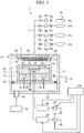
- FIG. 1 is a longitudinal cross-sectional view illustrating a schematic configuration of a plasma processing apparatus in accordance with an example embodiment.
- a plasma processing apparatus 1 includes a substantially cylindrical processing vessel 11 having therein a plasma processing space S in which a plasma process is performed.
- the processing vessel 11 is electrically grounded via a ground line 12. Further, a surface of the processing vessel 11 faces the plasma processing space S. That is, the processing vessel 11 is provided such that the surface thereof faces the plasma processing space S.
- a wafer chuck 10 configured to hold a wafer W as a target substrate.
- the wafer W held on the wafer chuck 10 is arranged such that a mask film D2 of the wafer W to be described later faces the plasma processing space S.
- a bottom surface of the wafer chuck 10 is supported on a susceptor 13 serving as a lower electrode.
- the susceptor 13 is made of a metal such as aluminum and has a substantially disk shape.
- a supporting table 15 is provided at a bottom of the processing vessel 11 via an insulating plate 14, and the susceptor 13 is supported on a top surface of the supporting table 15.
- An electrode (not illustrated) is embedded in the wafer chuck 10, and the wafer chuck 10 is configured to attract and hold the wafer W by an electrostatic force generated by applying a DC voltage to the electrode.
- a conductive focus ring 20 made of, for example, silicon is provided on an outer peripheral portion of the wafer chuck 10 as a top surface of the susceptor 13 in order to improve uniformity of a plasma process. Outer side surfaces of the susceptor 13, the supporting table 15, and the focus ring 20 are covered with a cylindrical member 21 made of, for example, quartz. Further, a surface of the focus ring 20 faces the plasma processing space S. That is, the focus ring 20 is provided such that the surface thereof faces the plasma processing space S.
- a coolant path 15a configured to allow a coolant to flow therein is formed into, for example, a circular ring shape.
- a temperature of the coolant supplied into the coolant path 15a a temperature of the wafer W held on the wafer chuck 10 can be controlled.
- a heat transfer gas line 22 configured to supply a heat transfer gas, e.g., a helium gas into a gap between the wafer chuck 10 and the wafer W held on the wafer chuck 10 is provided to pass through, for example, the susceptor 13, the supporting table 15, and the insulating plate 14.
- the susceptor 13 is electrically connected to a first high frequency power supply 30 configured to apply a high frequency power for plasma generation to the susceptor 13 via a first matching device 31.
- the first high supply power supply 30 is configured to output a high frequency power having a frequency of, for example, from 27 MHz to 100 MHz, e.g., 40 MHz in the present example embodiment.
- the first matching device 31 is configured to match internal impedance of the first high frequency power supply 30 with load impedance, and to allow the internal impedance of the first high frequency power supply 30 and the load impedance to be apparently matched with each other when plasma is generated within the processing vessel 11.
- the susceptor 13 is also electrically connected to a second high frequency power supply 40 configured to apply a bias voltage for ion attraction into the wafer W by applying a high frequency power to the susceptor 13 via a second matching device 41.
- the second high frequency power supply 40 is configured to output a high frequency power having a frequency of, for example, from 400 kHz to 13.56 MHz, e.g., 13.56 MHz in the present example embodiment.
- the frequency of the high frequency power outputted from the second high frequency power supply 40 is lower than the frequency of the high frequency power outputted from the first high frequency power supply 30.
- the second matching device 41 is also configured to match internal impedance of the second high frequency power supply 40 with load impedance.
- the high frequency power outputted from the first high frequency power supply 30 and the high frequency power outputted from the second high frequency power supply 40 may be referred to as a "high frequency power HF" and a "high frequency power LF", respectively.
- the first high frequency power supply 30, the first matching device 31, the second high frequency power supply 40, and the second matching device 41 are connected to a control unit 150 to be descried later, and the overall operations thereof are controlled by the control unit 150.
- an upper electrode 42 is provided above the susceptor 13 as the lower electrode.
- the upper electrode 42 is supported on a ceiling portion of the processing vessel 11 via a conductive supporting member 50. Accordingly, the upper electrode 42 is also electrically grounded like the processing vessel 11.
- the upper electrode 42 includes an electrode plate 51 that forms a surface of the upper electrode 42 facing the wafer W held on the wafer chuck 10; and an electrode supporting body 52 that supports the electrode plate 51 from above. Multiple gas discharge holes 53 configured to supply a processing gas into the processing vessel 11 are formed through the electrode plate 51.
- the electrode plate 51 is made of, for example, a semiconductor or a conductor having low Joule heat and low resistance, and in the present example embodiment, for example, silicon is used. Further, a surface of the electrode plate 51 facing the wafer W faces the plasma processing space S. That is, the electrode plate 51 is provided such that the surface thereof faces the plasma processing space S.
- the electrode supporting body 52 is made of a conductor, and in the present example embodiment, for example, aluminum is used.
- a gas diffusion space 54 having a substantially disk shape is formed in a central portion within the electrode supporting body 52.
- Multiple gas through holes 55 extended downwards from the gas diffusion space 54 are formed in a lower portion of the electrode supporting body 52, and the gas discharge holes 53 communicate with the gas diffusion space 54 via the gas through holes 55.
- the gas diffusion space 54 is connected to a gas supply line 71.
- the gas supply line 71 is connected to a processing gas supply source 72 as illustrated in FIG. 1 , and the processing gas supplied from the processing gas supply source 72 is introduced into the gas diffusion space 54 via the gas supply line 71.
- the processing gas introduced into the gas diffusion space 54 is then discharged into the processing vessel 11 through the gas through holes 55 and the gas discharge holes 53. That is, the upper electrode 42 serves as a shower head configured to supply the processing gas into the processing vessel 11.
- the processing gas supply source 72 includes a gas supply unit 72a, a gas supply unit 72b, a gas supply unit 72c, and a gas supply unit 72d.
- the gas supply unit 72a is configured to supply a first fluorine-containing gas as an etching gas into the plasma processing space S.
- the first fluorine-containing gas is, for example, a C 4 F 8 gas.
- the gas supply unit 72a is an example of the first gas supply unit configured to supply the first fluorine-containing gas into the plasma processing space S.
- the gas supply unit 72b is configured to supply an O 2 gas as a removing gas of deposit generated after an etching process into the plasma processing space S.
- the gas supply unit 72b is an example of the second gas supply unit configured to supply the O 2 gas into the plasma processing space S.
- the gas supply unit 72c is configured to supply a nitrogen-containing gas as a removing gas of deposit generated after the etching process into the plasma processing space S.
- the nitrogen-containing gas is, for example, at least one of a N 2 gas and a NF 3 gas.
- the gas supply unit 72d is configured to supply a second fluorine-containing gas as a removing gas of deposit generated after the etching process into the plasma processing space S.
- the second fluorine-containing gas is, for example, at least one of a CF 4 gas, a C 4 F 8 gas, and a CHF 3 gas.
- the gas supply unit 72c and the gas supply unit 72d are examples of the third gas supply unit configured to supply the nitrogen-containing gas and the second fluorine-containing gas into the plasma processing space S.
- the gas supply unit 72d may supply a third fluorine-containing gas as a removing gas of deposit generated after the etching process into the plasma processing space S.
- the third fluorine-containing gas is a gas containing C, H, and F, for example, a CHF 3 gas.
- the processing gas supply source 72 includes valves 73a, 73b, 73c, and 73d and flow rate controllers 74a, 74b, 74c, and 74d respectively provided between the gas supply units 72a, 72b, 72c, and 72d and the gas diffusion space 54.
- the flow rates of the gases supplied into the gas diffusion space 54 are controlled by the flow rate controllers 74a, 74b, 74c, and 74d.
- a gas exhaust path 80 serving as a flow path through which an atmosphere within the processing vessel 11 is exhausted to the outside of the processing vessel 11 is formed between an inner wall of the processing vessel 11 and an outer side surface of the cylindrical member 21 at a bottom portion of the processing vessel 11.
- a gas exhaust opening 90 is formed at a bottom surface of the processing vessel 11.
- a gas exhaust chamber 91 is provided under the gas exhaust opening 90, and a gas exhaust device 93 is connected to the gas exhaust chamber 91 via a gas exhaust line 92.
- control unit 150 is provided in the plasma processing apparatus 1.
- the control unit 150 is, for example, a computer including a program storage unit (not illustrated) as a storage device, for example, a memory.
- the program storage unit also stores a program for operating the plasma processing apparatus 1 by controlling the respective power supplies 30 and 40 or the respective matching devices 31 and 41 and the flow rate controller 74.
- the control unit 150 controls a process of supplying the first fluorine-containing gas from the gas supply unit 72a into the plasma processing space S and etching the wafer W with plasma of the first fluorine-containing gas.
- control unit 150 controls a process of supplying an O 2 gas from the gas supply unit 72b into the plasma processing space S and removing, with plasma of the O 2 gas, a carbon-containing material deposited on members (for example, the processing vessel 11, the electrode plate 51, and the focus ring 20), of which surfaces are arranged to face the plasma processing space S, after performing the etching process on the wafer W.
- members for example, the processing vessel 11, the electrode plate 51, and the focus ring 20
- control unit 150 controls a process of supplying the nitrogen-containing gas and the second fluorine-containing gas from the gas supply unit 72c and the gas supply unit 72d, respectively, into the plasma processing space S and removing, with plasma of the nitrogen-containing gas and the second fluorine-containing gas, a titanium-containing material deposited on the members, of which the surfaces are arranged to face the plasma processing space S, after performing the etching process on the wafer W.
- the program is stored in a computer readable storage medium such as a hard disk (HD), a flexible disk (FD), a compact disk (CD), a magneto-optical disk (MO), a memory card or the like and may be installed in the control unit 150 from the computer readable storage medium.
- a computer readable storage medium such as a hard disk (HD), a flexible disk (FD), a compact disk (CD), a magneto-optical disk (MO), a memory card or the like and may be installed in the control unit 150 from the computer readable storage medium.
- FIG. 2A is a diagram illustrating the example of a pre-etched wafer in the plasma processing apparatus in accordance with the example embodiment.
- FIG. 2B is a diagram illustrating an example of the post-etched wafer in the plasma processing apparatus in accordance with the example embodiment.
- the wafer W includes an insulating film D1 and a mask film D2 formed on a surface of the insulating film D1.
- the insulating film D1 is an interlayer insulating film for dual damascene wiring, and includes a first insulating film D11, a second insulating film D12, and a third insulating film D13.
- the first insulating film D11 is formed of, for example, SiON.
- the second insulating film D12 is formed of a material having a relative permittivity of a preset value (for example, 4.2) or less.
- the second insulating film D12 is formed of, for example, SiOCH.
- the third insulating film D13 is formed of, for example, SiCN.
- the mask film D2 on which an etching pattern having a preset opening is formed, is formed of a titanium-containing material having plasma resistance.
- the mask film D2 is formed of, for example, TiN.
- the wafer W on which the mask film D2 of the titanium-containing material (e.g., TiN, or the like) is formed on the surface of the insulating film D1, is arranged such that the mask film D2 faces the plasma processing space S.
- the wafer W is etched with the mask film D2 of TiN (hereinafter, appropriately referred to as "TiN film") as a mask
- the opening the opening of the mask film D2
- the insulating film D1 (the first insulating film D11 and the second insulating film D12) is etched.
- the TiN film itself may be etched as indicated by a dashed line in FIG. 2B . If the TiN film itself is etched, a carbon-containing material generated from the insulating film D1 and a titanium-containing material generated from the TiN film are deposited on the members (for example, the processing vessel 11, the electrode plate 51, and the focus ring 20), of which the surfaces are arranged to face the plasma processing space S. If the titanium-containing material is accumulatively deposited on the members of which the surfaces are arranged to face the plasma processing space S, plasma density within the plasma processing space S may not be uniform. As a result, the etching characteristics of the wafer W may be degraded with a lapse of time.
- the present inventor has repeated a close study on a method of removing a titanium-containing material deposited on the member, of which the surface is arranged to face the plasma processing space S, after performing the etching process on the wafer W with high efficiency.
- the present inventor has found out that it is possible to remove a titanium-containing material with high efficiency by removing a carbon-containing material with plasma of an O 2 gas and a titanium-containing material with plasma of a nitrogen-containing gas and a fluorine-containing gas.
- the reason for the above will be explained.
- the electrode plate 51 of the upper electrode 42 will be used, but it is not limited thereto.
- the member of which a surface is arranged to face the plasma processing space S can also be applied to the other members such as the processing vessel 11 and the focus ring 20.
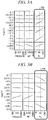
- FIG. 3A to FIG. 3D are diagrams each illustrating a result of experiments for selecting a factor contributing to removal of the titanium-containing material.
- a horizontal axis in FIG. 3A to FIG. 3D represents a value of each parameter contributing to the removal of the titanium-containing material in the experiment examples.
- a vertical axis in FIG. 3A and FIG. 3C represents Vpp (V) of the wafer W when the high frequency power HF is outputted from the first high frequency power supply 30.
- the Vpp denotes a difference between the maximum value and the minimum value of a voltage in the high frequency power on the surface of the wafer W. It can be seen that the Vpp correlates with plasma density caused by the high frequency power, and it can be found out that the variation in Vpp (V) corresponds to the variation in the plasma density.
- a gradient of the Vpp in the case of changing a flow rate of a N 2 gas to be supplied into the plasma processing space is higher than a gradient of the Vpp in the case of changing the other parameters. It is assumed that this is because plasma of the N 2 gas contributes to the removal of the TiN film formed on the wafer W.
- a gradient of the Vpp in the case of changing a flow rate of a CF 4 gas or a C 4 F 8 gas to be supplied into the plasma processing space is higher than a gradient of the Vpp in the case of changing the other parameters. It is assumed that this is because plasma of the CF 4 gas or the C 4 F 8 gas contributes to the removal of the TiN film formed on the wafer W. From the results of the experiments, a nitrogen-containing gas such as a N 2 gas and a fluorine-containing gas such as a CF 4 gas or a C 4 F 8 gas are selected as a factor most contributing to the removal of the titanium-containing material.
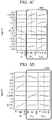
- FIG. 4 is a diagram illustrating an etching amount of the titanium-containing material for each member of which the surface is arranged to face the plasma processing space.
- FIG. 4 represents the etching amount [nm] of the TiN chip.
- a horizontal axis of FIG. 4 represents a position of the TiN chip arranged on each member.
- a graph 202 of FIG. 4 shows the etching amount of the TiN chip arranged on a central portion of the electrode plate 51 (hereinafter, referred to as "electrode plate central chip") when the electrode plate central chip is etched with plasma of an O 2 gas.
- a graph 204 shows the etching amount of the electrode plate central chip when the electrode plate central chip is etched with plasma of a CHF 3 gas after etching the chip with the plasma of the O 2 gas.
- a graph 206 shows the etching amount of the electrode plate central chip when the electrode plate central chip is etched with plasma of a N 2 gas and a C 4 F 8 gas after etching the chip with the plasma of the CHF 3 gas.
- a graph 212 shows the etching amount of the TiN chip arranged on a peripheral portion of the electrode plate 51 (hereinafter, referred to as "electrode plate peripheral chip") when the electrode plate peripheral chip is etched with plasma of an O 2 gas.
- a graph 214 shows the etching amount of the electrode plate peripheral chip when the electrode plate peripheral chip is etched with plasma of a CHF 3 gas after etching the chip with the plasma of the O 2 gas.
- a graph 216 shows the etching amount of the electrode plate peripheral chip when the electrode plate peripheral chip is etched with plasma of a N 2 gas and a C 4 F 8 gas after etching the chip with the plasma of the CHF 3 gas.
- a graph 222 shows the etching amount of the TiN chip arranged on the focus ring 20 (hereinafter, referred to as "focus ring chip") when the focus ring chip is etched with plasma of an O 2 gas.
- a graph 224 shows the etching amount of the focus ring chip when the focus ring chip is etched with plasma of a CHF 3 gas after etching the chip with the plasma of the O 2 gas.
- a graph 226 shows the etching amount of the focus ring chip when the focus ring chip is etched with plasma of a N 2 gas and a C 4 F 8 gas after etching the chip with the plasma of the CHF 3 gas.
- the etching amount of the electrode plate central chip is the highest. Further, through the comparison between the graph 212 and the graphs 214 and 216, when the electrode plate peripheral chip is etched with the plasma of the N 2 gas and the C 4 F 8 gas as shown in the graph 216, the etching amount of the electrode plate peripheral chip is the highest. Furthermore, through the comparison between the graph 222 and the graphs 224 and 226, when the focus ring chip is etched with the plasma of the N 2 gas and the C 4 F 8 gas, the etching amount of the focus ring chip is the highest.
- titanium-containing material deposited on the electrode plate 51 or the focus ring 20 chemically reacts with the plasma of the N 2 gas and the C 4 F 8 gas to generate a complex gas such as Ti(NF 3 ), so that the titanium-containing material deposited on the electrode plate 51 or the focus ring 20 can be removed.
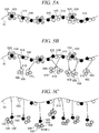
- FIG. 5A to FIG. 5C are diagrams each illustrating a plasma process model in accordance with the present example embodiment.
- a molecular model group 510 is a carbon model contained in the carbon-containing material deposited on the electrode plate 51 after performing the etching process on the wafer W.
- a molecular model group 520 is a titanium model contained in the titanium-containing material (e.g., TiF 4 , TiN, TiO 2 , Ti, and the like) deposited on the electrode plate 51 after performing the etching process on the wafer W.
- TiF 4 titanium model contained in the titanium-containing material
- a molecular model group 530 is a fluorine model contained in the titanium-containing material (e.g ., TiF 4 and the like) deposited on the electrode plate 51 after performing the etching process on the wafer W.
- a molecular model group 540 is a nitrogen model contained in the titanium-containing material (e.g., TiN and the like) deposited on the electrode plate 51 after performing the etching process on the wafer W.
- a molecular model group 550 is an oxygen model.
- a first process of supplying the first fluorine-containing gas (e.g., C 4 F 8 gas) into the plasma processing space S and etching the wafer W with plasma of the first fluorine-containing gas is performed.
- the first fluorine-containing gas e.g., C 4 F 8 gas
- the carbon-containing material molecular model group 510 generated from the etched insulating film on the wafer W
- the titanium-containing materials the molecular model group 520, the molecular model group 530, and the molecular model group 540
- a second process of supplying an O 2 gas into the plasma processing space S and removing, with plasma of the O 2 gas, the carbon-containing material deposited on the electrode plate 51 after performing the first process is performed.
- the carbon-containing material on the surface of the electrode plate 51 chemically reacts with the plasma of the O 2 gas to generate CO or CO 2 , so that the carbon-containing material is removed from the surface of the electrode plate 51.
- the second process may be referred to as "carbon-containing material removal process”.
- a third process of supplying the nitrogen-containing gas (e.g., N 2 gas or a NF 3 gas) and the second fluorine-containing gas (e.g., CF 4 gas, a C 4 F 8 gas, or CHF 3 gas) into the plasma processing space S and removing, with plasma of the nitrogen-containing gas and the second fluorine-containing gas, the titanium-containing material deposited on the electrode plate 51 after performing the first process is performed.
- the nitrogen-containing gas e.g., N 2 gas or a NF 3 gas
- the second fluorine-containing gas e.g., CF 4 gas, a C 4 F 8 gas, or CHF 3 gas
- the titanium-containing material on the surface of the electrode plate 51 chemically reacts with the plasma of the nitrogen-containing gas and the second fluorine-containing gas to generate a complex gas such as Ti(NF 3 ), so that the titanium-containing material is removed from the surface of the electrode plate 51.
- the third process may be referred to as "titanium-containing material removal process".
- the plasma processing apparatus 1 supplies the first fluorine-containing gas and etches the wafer W with the plasma of the first fluorine-containing gas in the first process. Further, in the plasma process of the present example embodiment, the plasma processing apparatus 1 supplies the O 2 gas into the plasma processing space S and removes, with the plasma of the O 2 gas, the carbon-containing material deposited on the electrode plate 51 after the first process in the second process, so that the titanium-containing material on the surface of the electrode plate 51 is exposed.
- the plasma processing apparatus 1 supplies the nitrogen-containing gas and the second fluorine-containing gas into the plasma processing space S and removes, with the plasma of the nitrogen-containing gas and the second fluorine-containing gas, the titanium-containing material deposited on the electrode plate 51 after the first process in the third process, so that the complex gas such as Ti(NF 3 ) is generated.
- the plasma processing apparatus 1 supplies the nitrogen-containing gas and the second fluorine-containing gas into the plasma processing space S and removes, with the plasma of the nitrogen-containing gas and the second fluorine-containing gas, the titanium-containing material deposited on the electrode plate 51 after the first process in the third process, so that the complex gas such as Ti(NF 3 ) is generated.
- FIG. 6 is a flow chart of a plasma process in accordance with a first experimental example.
- the etching process is performed (process S101).
- the control unit 150 controls the flow rate controller 74a to supply the first fluorine-containing gas into the plasma processing space S. Then, the control unit 150 controls the first high frequency power supply 30 and the second high frequency power supply 40 to excite the first fluorine-containing gas into plasma to etch the wafer W with the plasma of the first fluorine-containing gas.
- the carbon-containing material removal process is performed (process S102).
- the control unit 150 controls the flow rate controller 74b to supply the O 2 gas into the plasma processing space S.
- the control unit 150 controls the first high frequency power supply 30 and the second high frequency power supply 40 to excite the O 2 gas into plasma and removes, with the plasma of the O 2 gas, the carbon-containing material deposited on the electrode plate 51, of which the surface is arranged to face the plasma processing space S.
- the titanium-containing material removal process is performed (process S103).
- the control unit 150 controls the flow rate controller 74c and the flow rate controller 74d to supply the nitrogen-containing gas and the second fluorine-containing gas, respectively, into the plasma processing space S.
- the control unit 150 controls the first high frequency power supply 30 and the second high frequency power supply 40 to excite the nitrogen-containing gas and the second fluorine-containing gas into plasma and removes, with the plasma of the nitrogen-containing gas and the second fluorine-containing gas, the titanium-containing material deposited on the electrode plate 51, of which the surface is arranged to face the plasma processing space S.
- the wafer W is etched through the etching process, and the carbon-containing material deposited on the electrode plate 51 is removed through the carbon-containing material removal process, so that the titanium-containing material is exposed. Then, the titanium-containing material as a complex gas, e.g., Ti(NF 3 ) is removed through the titanium-containing material removal process. For this reason, even if deposits such as the titanium-containing material generated from the wafer W during the etching process are deposited on the electrode plate 51, it is possible to remove the titanium-containing material of the deposits with high efficiency. Therefore, it is possible to suppress the variation in the plasma density within the plasma processing space. As a result, it is possible to suppress the etching characteristics of the wafer W from being degraded with a lapse of time.
- Ti(NF 3 ) complex gas
- FIG. 7 is a flow chart of a plasma process in accordance with the second experimental example.
- the etching process is performed (process S201).
- the control unit 150 controls the flow rate controller 74a to supply the first fluorine-containing gas into the plasma processing space S. Then, the control unit 150 controls the first high frequency power supply 30 and the second high frequency power supply 40 to excite the first fluorine-containing gas into plasma to etch the wafer W with the plasma of the first fluorine-containing gas.
- the titanium-containing material removal process is performed (process S202).
- the control unit 150 controls the flow rate controller 74c and the flow rate controller 74d to supply the nitrogen-containing gas and the second fluorine-containing gas, respectively, into the plasma processing space S.
- the control unit 150 controls the first high frequency power supply 30 and the second high frequency power supply 40 to excite the nitrogen-containing gas and the second fluorine-containing gas into plasma and removes, with the plasma of the nitrogen-containing gas and the second fluorine-containing gas, the titanium-containing material deposited on the electrode plate 51, of which the surface is arranged to face the plasma processing space S.
- the carbon-containing material removal process is performed (process S203).
- the control unit 150 controls the flow rate controller 74b to supply the O 2 gas into the plasma processing space S.
- the control unit 150 controls the first high frequency power supply 30 and the second high frequency power supply 40 to excite the O 2 gas into plasma and removes, with the plasma of the O 2 gas, the carbon-containing material deposited on the electrode plate 51, of which the surface is arranged to face the plasma processing space S.
- the wafer W is etched through the etching process, and the titanium-containing material deposited on the electrode plate 51 as a complex gas, e.g., Ti(NF 3 ) is removed through the titanium-containing material removal process, so that the carbon-containing material is exposed. Then, the carbon-containing material is removed through the carbon-containing material removal process. For this reason, even if deposits such as a titanium-containing material generated from the wafer W during the etching process are deposited on the electrode plate 51, it is possible to remove the titanium-containing material of the deposits with high efficiency. Therefore, it is possible to suppress the variation in the plasma density within the plasma processing space. As a result, it is possible to suppress the etching characteristics of the wafer W from being degraded with a lapse of time.
- a complex gas e.g., Ti(NF 3 )
- FIG. 8 is a flow chart of a plasma process in accordance with the third experimental example.
- the etching process is performed (process S301).
- the control unit 150 controls the flow rate controller 74a to supply the first fluorine-containing gas into the plasma processing space S. Then, the control unit 150 controls the first high frequency power supply 30 and the second high frequency power supply 40 to excite the first fluorine-containing gas into plasma to etch the wafer W with the plasma of the first fluorine-containing gas.
- a first carbon-containing material removal process is performed (process S302).
- the control unit 150 controls the flow rate controller 74b to supply the O 2 gas into the plasma processing space S.
- the control unit 150 controls the first high frequency power supply 30 and the second high frequency power supply 40 to excite the O 2 gas into plasma and removes, with the plasma of the O 2 gas, the carbon-containing material deposited on the electrode plate 51, of which the surface is arranged to face the plasma processing space S.
- a first titanium-containing material removal process is performed (process S303).
- the control unit 150 controls the flow rate controller 74c and the flow rate controller 74d to supply the nitrogen-containing gas and the second fluorine-containing gas, respectively, into the plasma processing space S.
- the control unit 150 controls the first high frequency power supply 30 and the second high frequency power supply 40 to excite the nitrogen-containing gas and the second fluorine-containing gas into plasma and removes, with the plasma of the nitrogen-containing gas and the second fluorine-containing gas, the titanium-containing material deposited on the electrode plate 51, of which the surface is arranged to face the plasma processing space S.
- a second carbon-containing material removal process is performed (process S304).
- the control unit 150 controls the flow rate controller 74b to supply the O 2 gas into the plasma processing space S.
- the control unit 150 controls the first high frequency power supply 30 and the second high frequency power supply 40 to excite the O 2 gas into plasma and removes, with the plasma of the O 2 gas, the carbon-containing material deposited on the electrode plate 51, of which the surface is arranged to face the plasma processing space S.
- a second titanium-containing material removal process is performed (process S305).
- the control unit 150 controls the flow rate controller 74c and the flow rate controller 74d to supply the nitrogen-containing gas and the second fluorine-containing gas, respectively, into the plasma processing space S.
- the control unit 150 controls the first high frequency power supply 30 and the second high frequency power supply 40 to excite the nitrogen-containing gas and the second fluorine-containing gas into plasma and removes, with the plasma of the nitrogen-containing gas and the second fluorine-containing gas, the titanium-containing material deposited on the electrode plate 51, of which the surface is arranged to face the plasma processing space S.
- the wafer W is etched through the etching process, the carbon-containing material deposited on the electrode plate 51 is removed through the carbon-containing material removal process, so that the titanium-containing material is exposed. Then, the titanium-containing material as a complex gas, e.g., Ti(NF 3 ) is removed through the titanium-containing material removal process. For this reason, even if deposits such as a titanium-containing material generated from the wafer W during the etching process are deposited on the electrode plate 51, it is possible to remove the titanium-containing material of the deposits with high efficiency. Therefore, it is possible to suppress the variation in the plasma density within the plasma processing space.
- a complex gas e.g., Ti(NF 3 )
- the plasma process in accordance with the third experimental example shows an example where the set of the carbon-containing material removal process and the titanium-containing material removal process is repeatedly performed twice after the etching process, the set of the carbon-containing material removal process and the titanium-containing material removal process may be repeatedly performed twice or more times after the etching process.
- FIG. 9 is a flow chart of a plasma process in accordance with a fourth experimental example.
- the etching process is performed (process S401).
- the control unit 150 controls the flow rate controller 74a to supply the first fluorine-containing gas into the plasma processing space S. Then, the control unit 150 controls the first high frequency power supply 30 and the second high frequency power supply 40 to excite the first fluorine-containing gas into plasma to etch the wafer W with the plasma of the first fluorine-containing gas.
- the carbon-containing material removal process is performed (process S402).
- the control unit 150 controls the flow rate controller 74b to supply the O 2 gas into the plasma processing space S.
- the control unit 150 controls the first high frequency power supply 30 and the second high frequency power supply 40 to excite the O 2 gas into plasma and removes, with the plasma of the O 2 gas, the carbon-containing material deposited on the electrode plate 51, of which the surface is arranged to face the plasma processing space S.
- a titanium-containing material removal process using a CHF 3 gas is performed (process S403).
- the control unit 150 controls the flow rate controller 74d or the like to supply a CHF 3 gas as a third fluorine-containing gas into the plasma processing space S.
- the control unit 150 controls the first high frequency power supply 30 and the second high frequency power supply 40 to excite the CHF 3 gas into plasma and removes, with the plasma of the CHF 3 gas, the titanium-containing material deposited on the electrode plate 51, of which the surface is arranged to face the plasma processing space S.
- the titanium-containing material removal process is performed (process S404).
- the control unit 150 controls the flow rate controller 74c and the flow rate controller 74d to supply the nitrogen-containing gas and the second fluorine-containing gas, respectively, into the plasma processing space S.
- the control unit 150 controls the first high frequency power supply 30 and the second high frequency power supply 40 to excite the nitrogen-containing gas and the second fluorine-containing gas into plasma and removes, with the plasma of the nitrogen-containing gas and the second fluorine-containing gas, the titanium-containing material deposited on the electrode plate 51, of which the surface is arranged to face the plasma processing space S.
- the wafer W is etched through the etching process, and the carbon-containing material deposited on the electrode plate 51 is removed through the carbon-containing material removal process, so that the titanium-containing material is exposed. Then, the titanium-containing material as a complex gas, e.g ., Ti(NF 3 ) is removed through the titanium-containing material removal process. For this reason, even if deposits such as a titanium-containing material generated from the wafer W during the etching process are deposited on the electrode plate 51, it is possible to remove the titanium-containing material of the deposits with high efficiency. Therefore, it is possible to suppress the variation in the plasma density within the plasma processing space.
- a complex gas e.g ., Ti(NF 3 )
- the CHF 3 gas as the third fluorine-containing gas is supplied into the plasma processing space to remove the titanium-containing material deposited on the electrode plate 51 with the plasma of the CHF 3 gas. As a result, it is possible to remove the deposits deposited on the electrode plate 51 with higher efficiency.
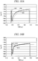
- FIG. 10A and FIG. 10B are diagrams for explaining an effect of the plasma processing method in accordance with the present example embodiment.
- FIG. 10A and FIG. 10B are diagrams each showing an effect when a plasma process is performed on the wafer W in the plasma processing apparatus 1.
- a horizontal axis represents a time (sec) during which the plasma process is performed on the wafer W in the plasma processing apparatus 1
- a vertical axis represents the Vpp (V) on the wafer W.
- the Vpp denotes a difference between the maximum value and the minimum value of a voltage in the high frequency power on the surface of the wafer W. It can be seen that the Vpp correlates with the plasma density caused by the high frequency power, and it can be found out that the variation in the Vpp (V) corresponds to the variation in the plasma density.
- FIG. 10A is a graph showing a relationship between the Vpp on the wafer W for lot numbers during a dry cleaning (DC) process and the processing time in the case of performing the DC process on the wafer W with the plasma of the O 2 gas without using the plasma processing method in accordance with the present example embodiment. That is, a graph 602 in FIG. 10A shows a relationship between the Vpp and the processing time when the etching process is performed on a groove for dual damascene wiring with respect to 25 wafers W in lot number "1" (see FIG. 2 ) and then, the DC process is performed.
- DC dry cleaning
- a graph 604 shows a relationship between the Vpp and the processing time in the DC process after processing 25 wafers W in lot number "2" (i.e., after accumulatively processing 50 wafers W including lot number “1”).
- a graph 606 shows a relationship between the Vpp and the processing time in the DC process after processing 25 wafers W in lot number "3" ( i.e., after accumulatively processing 75 wafers W including lot numbers "1” and "2").
- FIG. 10B is a graph showing a relationship between the Vpp on the wafer W for lot numbers and the processing time in the case of performing the plasma process on the wafer W using the plasma processing method in accordance with the present example embodiment. That is, a graph 612 in FIG.
- FIG. 10B shows a relationship between the Vpp and the processing time when the etching process is performed on a groove for dual damascene wiring with respect to 25 wafers W in lot number "1" (see FIG. 2 ) and the plasma process in accordance with the present example embodiment is performed and then, the DC process is performed.
- the graph 612 shows an effect in the case of performing the plasma process in accordance with the present example embodiment before the DC process of FIG. 10A .
- a graph 614 shows a relationship between the Vpp and the processing time in the DC process after processing 25 wafers W in lot number "2" ( i.e., accumulatively processing 50 wafers W including lot number "1") and the plasma process in accordance with the present example embodiment.
- a graph 616 shows a relationship between the Vpp and the processing time in the DC process after processing 25 wafers W in lot number "3" (i.e., after accumulatively processing 75 wafers W including lot numbers "1" and "2") and the plasma process in accordance with the present example embodiment.
- the variations of the Vpp on the wafer W with respect to the processing time are different according to a difference in a lot number as shown in the graphs 602, 604, and 606. It is assumed that this is because the titanium-containing material generated from the mask film on the wafer W during the etching process is accumulatively deposited on the electrode plate 51 facing the plasma processing space and the plasma density within the plasma processing space is varied.
- the carbon-containing material deposited on the electrode plate 51 is removed through the carbon-containing material removal process and the titanium-containing material deposited on the electrode plate 51 is removed through the titanium-containing material removal process.
- the variations of the Vpp on the wafer W with respect to the processing time are equivalently maintained regardless of the lot number.
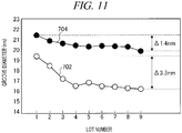
- FIG. 11 is a diagram for explaining an effect of the plasma processing method in accordance with the present example embodiment.
- a horizontal axis in FIG. 11 represents a lot number (cumulative value) of the wafers W loaded into the plasma processing apparatus 1, and a vertical axis represents a diameter (nm) of a groove formed on the insulating film when the insulating film on the wafer W is etched.
- a graph 702 shows changes in the diameter of the groove formed on the insulating film with respect to the lot number (cumulative value) in the case of performing the DC process only without using the plasma processing method in accordance with the present example embodiment.
- a graph 704 shows changes in the diameter of the groove formed on the insulating film with respect to the lot number in the case of performing the plasma processing method in accordance with the present example embodiment.
- the decrement in the diameter of the groove formed on the insulating film with respect to the lot number in the case of performing the plasma processing method in accordance with the present example embodiment is smaller than that in the case of performing the DC process only. It is assumed that this is because in the case of performing the plasma processing method in accordance with the present example embodiment, even when the titanium-containing material generated from the mask film of the wafer W during the etching process is deposited on the electrode plate 51 facing the plasma processing space, the titanium-containing material deposited on the electrode plate 51 is removed. As a result, it can be seen that the plasma density becomes stable and the change in the etched groove shape is suppressed accordingly.
Landscapes
- Engineering & Computer Science (AREA)
- Chemical & Material Sciences (AREA)
- Physics & Mathematics (AREA)
- Plasma & Fusion (AREA)
- Analytical Chemistry (AREA)
- Computer Hardware Design (AREA)
- Power Engineering (AREA)
- Microelectronics & Electronic Packaging (AREA)
- Condensed Matter Physics & Semiconductors (AREA)
- General Physics & Mathematics (AREA)
- Manufacturing & Machinery (AREA)
- Epidemiology (AREA)
- Health & Medical Sciences (AREA)
- Public Health (AREA)
- Inorganic Chemistry (AREA)
- General Chemical & Material Sciences (AREA)
- Chemical Kinetics & Catalysis (AREA)
- Materials Engineering (AREA)
- Mechanical Engineering (AREA)
- Metallurgy (AREA)
- Organic Chemistry (AREA)
- Drying Of Semiconductors (AREA)
- Plasma Technology (AREA)
Applications Claiming Priority (3)
| Application Number | Priority Date | Filing Date | Title |
|---|---|---|---|
| JP2012186344A JP5982223B2 (ja) | 2012-08-27 | 2012-08-27 | プラズマ処理方法、及びプラズマ処理装置 |
| US201261695630P | 2012-08-31 | 2012-08-31 | |
| PCT/JP2013/071409 WO2014034396A1 (ja) | 2012-08-27 | 2013-08-07 | プラズマ処理方法、及びプラズマ処理装置 |
Publications (3)
| Publication Number | Publication Date |
|---|---|
| EP2879166A1 EP2879166A1 (en) | 2015-06-03 |
| EP2879166A4 EP2879166A4 (en) | 2016-03-16 |
| EP2879166B1 true EP2879166B1 (en) | 2019-10-09 |
Family
ID=50183214
Family Applications (1)
| Application Number | Title | Priority Date | Filing Date |
|---|---|---|---|
| EP13833486.7A Active EP2879166B1 (en) | 2012-08-27 | 2013-08-07 | Plasma processing method |
Country Status (7)
Families Citing this family (10)
| Publication number | Priority date | Publication date | Assignee | Title |
|---|---|---|---|---|
| JP6049527B2 (ja) * | 2013-04-05 | 2016-12-21 | 東京エレクトロン株式会社 | プラズマ処理方法及びプラズマ処理装置 |
| JP2017045849A (ja) * | 2015-08-26 | 2017-03-02 | 東京エレクトロン株式会社 | シーズニング方法およびエッチング方法 |
| WO2017123423A1 (en) * | 2016-01-13 | 2017-07-20 | Applied Materials, Inc. | Hydrogen plasma based cleaning process for etch hardware |
| CN107369603A (zh) * | 2016-05-12 | 2017-11-21 | 中芯国际集成电路制造(上海)有限公司 | 去除含氧副产物、清洗刻蚀腔和形成半导体结构的方法 |
| JP6785101B2 (ja) * | 2016-09-09 | 2020-11-18 | 東京エレクトロン株式会社 | プラズマエッチング方法 |
| JP6763750B2 (ja) * | 2016-11-07 | 2020-09-30 | 東京エレクトロン株式会社 | 被処理体を処理する方法 |
| CN110476483A (zh) * | 2017-04-14 | 2019-11-19 | 堺显示器制品株式会社 | 有机el显示装置的制造方法及制造装置 |
| CN110637357A (zh) * | 2017-06-21 | 2019-12-31 | 惠普印迪格公司 | 真空工作台 |
| CN109962001A (zh) * | 2017-12-26 | 2019-07-02 | 中微半导体设备(上海)股份有限公司 | 一种等离子体腔室的运行方法和等离子反应器 |
| KR20240129072A (ko) * | 2022-01-13 | 2024-08-27 | 램 리써치 코포레이션 | 높은 선택도 및 균일한 유전체 에칭 |
Family Cites Families (16)
| Publication number | Priority date | Publication date | Assignee | Title |
|---|---|---|---|---|
| JPH03239323A (ja) * | 1990-02-16 | 1991-10-24 | Yamaha Corp | ドライエッチング方法 |
| JP3117187B2 (ja) * | 1995-12-20 | 2000-12-11 | 株式会社日立製作所 | プラズマクリーニング処理方法 |
| US5948702A (en) * | 1996-12-19 | 1999-09-07 | Texas Instruments Incorporated | Selective removal of TixNy |
| JPH10280151A (ja) * | 1997-04-08 | 1998-10-20 | Fujitsu Ltd | Cvd装置のクリーニング方法 |
| US6692903B2 (en) * | 2000-12-13 | 2004-02-17 | Applied Materials, Inc | Substrate cleaning apparatus and method |
| JP4176365B2 (ja) * | 2002-03-25 | 2008-11-05 | 東京エレクトロン株式会社 | プラズマエッチング方法 |
| US20060016783A1 (en) * | 2004-07-22 | 2006-01-26 | Dingjun Wu | Process for titanium nitride removal |
| JP2006165246A (ja) * | 2004-12-07 | 2006-06-22 | Tokyo Electron Ltd | プラズマエッチング方法 |
| US7488689B2 (en) * | 2004-12-07 | 2009-02-10 | Tokyo Electron Limited | Plasma etching method |
| JP5047504B2 (ja) | 2005-02-05 | 2012-10-10 | 三星電子株式会社 | ビアキャッピング保護膜を使用する半導体素子のデュアルダマシン配線の製造方法 |
| JP4764028B2 (ja) * | 2005-02-28 | 2011-08-31 | 株式会社日立ハイテクノロジーズ | プラズマ処理方法 |
| JP4288252B2 (ja) * | 2005-04-19 | 2009-07-01 | パナソニック株式会社 | 半導体チップの製造方法 |
| JP2008198659A (ja) * | 2007-02-08 | 2008-08-28 | Tokyo Electron Ltd | プラズマエッチング方法 |
| JP5705495B2 (ja) * | 2010-10-07 | 2015-04-22 | 株式会社日立ハイテクノロジーズ | プラズマの処理方法及びプラズマ処理装置 |
| US20120094499A1 (en) * | 2010-10-15 | 2012-04-19 | Siu Tang Ng | Method of performing an in situ chamber clean |
| JP6177601B2 (ja) * | 2013-06-25 | 2017-08-09 | 東京エレクトロン株式会社 | クリーニング方法及び基板処理装置 |
-
2012
- 2012-08-27 JP JP2012186344A patent/JP5982223B2/ja active Active
-
2013
- 2013-08-07 WO PCT/JP2013/071409 patent/WO2014034396A1/ja active Application Filing
- 2013-08-07 US US14/424,217 patent/US9460896B2/en active Active
- 2013-08-07 CN CN201380039947.7A patent/CN104508803B/zh active Active
- 2013-08-07 KR KR1020157005120A patent/KR102114922B1/ko active Active
- 2013-08-07 EP EP13833486.7A patent/EP2879166B1/en active Active
- 2013-08-23 TW TW102130274A patent/TWI571930B/zh active
Non-Patent Citations (1)
| Title |
|---|
| None * |
Also Published As
| Publication number | Publication date |
|---|---|
| JP2014045063A (ja) | 2014-03-13 |
| TWI571930B (zh) | 2017-02-21 |
| JP5982223B2 (ja) | 2016-08-31 |
| US9460896B2 (en) | 2016-10-04 |
| KR102114922B1 (ko) | 2020-05-25 |
| US20150228458A1 (en) | 2015-08-13 |
| KR20150048134A (ko) | 2015-05-06 |
| CN104508803A (zh) | 2015-04-08 |
| WO2014034396A1 (ja) | 2014-03-06 |
| CN104508803B (zh) | 2016-12-07 |
| TW201413817A (zh) | 2014-04-01 |
| EP2879166A4 (en) | 2016-03-16 |
| EP2879166A1 (en) | 2015-06-03 |
Similar Documents
| Publication | Publication Date | Title |
|---|---|---|
| EP2879166B1 (en) | Plasma processing method | |
| US9735021B2 (en) | Etching method | |
| JP6339963B2 (ja) | エッチング方法 | |
| JP5390846B2 (ja) | プラズマエッチング装置及びプラズマクリーニング方法 | |
| US20200381263A1 (en) | Method of processing target object | |
| US9087676B2 (en) | Plasma processing method and plasma processing apparatus | |
| US9818582B2 (en) | Plasma processing method | |
| US9147556B2 (en) | Plasma processing method and plasma processing apparatus | |
| TW201919127A (zh) | 改良之金屬接觸定位結構 | |
| JP2008078515A (ja) | プラズマ処理方法 | |
| US9653317B2 (en) | Plasma processing method and plasma processing apparatus | |
| US20140256147A1 (en) | Plasma processing apparatus and plasma processing method | |
| KR20190008227A (ko) | 에칭 방법 | |
| JP2016086046A (ja) | プラズマ処理方法 | |
| US9953862B2 (en) | Plasma processing method and plasma processing apparatus | |
| KR101909784B1 (ko) | 상부 전극의 표면 처리 방법, 플라즈마 처리 장치 및 상부 전극 | |
| TW201618156A (zh) | 電漿處理裝置及電漿處理方法 | |
| JP2007266296A (ja) | 基板処理装置及び側壁部品 | |
| US9711371B2 (en) | Method of etching organic film | |
| CN111326395A (zh) | 等离子体处理方法和等离子体处理装置 | |
| KR20240121860A (ko) | 플라스마 처리 장치 | |
| JP2015106587A (ja) | 静電チャックのコーティング方法及びプラズマ処理装置 |
Legal Events
| Date | Code | Title | Description |
|---|---|---|---|
| PUAI | Public reference made under article 153(3) epc to a published international application that has entered the european phase |
Free format text: ORIGINAL CODE: 0009012 |
|
| 17P | Request for examination filed |
Effective date: 20150227 |
|
| AK | Designated contracting states |
Kind code of ref document: A1 Designated state(s): AL AT BE BG CH CY CZ DE DK EE ES FI FR GB GR HR HU IE IS IT LI LT LU LV MC MK MT NL NO PL PT RO RS SE SI SK SM TR |
|
| AX | Request for extension of the european patent |
Extension state: BA ME |
|
| DAX | Request for extension of the european patent (deleted) | ||
| RA4 | Supplementary search report drawn up and despatched (corrected) |
Effective date: 20160215 |
|
| RIC1 | Information provided on ipc code assigned before grant |
Ipc: H01L 21/311 20060101ALI20160209BHEP Ipc: H01J 37/32 20060101ALI20160209BHEP Ipc: H01L 21/3065 20060101AFI20160209BHEP Ipc: H05H 1/46 20060101ALI20160209BHEP |
|
| GRAP | Despatch of communication of intention to grant a patent |
Free format text: ORIGINAL CODE: EPIDOSNIGR1 |
|
| STAA | Information on the status of an ep patent application or granted ep patent |
Free format text: STATUS: GRANT OF PATENT IS INTENDED |
|
| INTG | Intention to grant announced |
Effective date: 20190411 |
|
| GRAS | Grant fee paid |
Free format text: ORIGINAL CODE: EPIDOSNIGR3 |
|
| GRAA | (expected) grant |
Free format text: ORIGINAL CODE: 0009210 |
|
| STAA | Information on the status of an ep patent application or granted ep patent |
Free format text: STATUS: THE PATENT HAS BEEN GRANTED |
|
| AK | Designated contracting states |
Kind code of ref document: B1 Designated state(s): AL AT BE BG CH CY CZ DE DK EE ES FI FR GB GR HR HU IE IS IT LI LT LU LV MC MK MT NL NO PL PT RO RS SE SI SK SM TR |
|
| REG | Reference to a national code |
Ref country code: GB Ref legal event code: FG4D |
|
| REG | Reference to a national code |
Ref country code: CH Ref legal event code: EP |
|
| REG | Reference to a national code |
Ref country code: IE Ref legal event code: FG4D |
|
| REG | Reference to a national code |
Ref country code: DE Ref legal event code: R096 Ref document number: 602013061586 Country of ref document: DE |
|
| REG | Reference to a national code |
Ref country code: AT Ref legal event code: REF Ref document number: 1189799 Country of ref document: AT Kind code of ref document: T Effective date: 20191115 |
|
| REG | Reference to a national code |
Ref country code: NL Ref legal event code: MP Effective date: 20191009 |
|
| REG | Reference to a national code |
Ref country code: LT Ref legal event code: MG4D |
|
| REG | Reference to a national code |
Ref country code: AT Ref legal event code: MK05 Ref document number: 1189799 Country of ref document: AT Kind code of ref document: T Effective date: 20191009 |
|
| PG25 | Lapsed in a contracting state [announced via postgrant information from national office to epo] |
Ref country code: NO Free format text: LAPSE BECAUSE OF FAILURE TO SUBMIT A TRANSLATION OF THE DESCRIPTION OR TO PAY THE FEE WITHIN THE PRESCRIBED TIME-LIMIT Effective date: 20200109 Ref country code: PL Free format text: LAPSE BECAUSE OF FAILURE TO SUBMIT A TRANSLATION OF THE DESCRIPTION OR TO PAY THE FEE WITHIN THE PRESCRIBED TIME-LIMIT Effective date: 20191009 Ref country code: NL Free format text: LAPSE BECAUSE OF FAILURE TO SUBMIT A TRANSLATION OF THE DESCRIPTION OR TO PAY THE FEE WITHIN THE PRESCRIBED TIME-LIMIT Effective date: 20191009 Ref country code: PT Free format text: LAPSE BECAUSE OF FAILURE TO SUBMIT A TRANSLATION OF THE DESCRIPTION OR TO PAY THE FEE WITHIN THE PRESCRIBED TIME-LIMIT Effective date: 20200210 Ref country code: LT Free format text: LAPSE BECAUSE OF FAILURE TO SUBMIT A TRANSLATION OF THE DESCRIPTION OR TO PAY THE FEE WITHIN THE PRESCRIBED TIME-LIMIT Effective date: 20191009 Ref country code: ES Free format text: LAPSE BECAUSE OF FAILURE TO SUBMIT A TRANSLATION OF THE DESCRIPTION OR TO PAY THE FEE WITHIN THE PRESCRIBED TIME-LIMIT Effective date: 20191009 Ref country code: SE Free format text: LAPSE BECAUSE OF FAILURE TO SUBMIT A TRANSLATION OF THE DESCRIPTION OR TO PAY THE FEE WITHIN THE PRESCRIBED TIME-LIMIT Effective date: 20191009 Ref country code: LV Free format text: LAPSE BECAUSE OF FAILURE TO SUBMIT A TRANSLATION OF THE DESCRIPTION OR TO PAY THE FEE WITHIN THE PRESCRIBED TIME-LIMIT Effective date: 20191009 Ref country code: AT Free format text: LAPSE BECAUSE OF FAILURE TO SUBMIT A TRANSLATION OF THE DESCRIPTION OR TO PAY THE FEE WITHIN THE PRESCRIBED TIME-LIMIT Effective date: 20191009 Ref country code: FI Free format text: LAPSE BECAUSE OF FAILURE TO SUBMIT A TRANSLATION OF THE DESCRIPTION OR TO PAY THE FEE WITHIN THE PRESCRIBED TIME-LIMIT Effective date: 20191009 Ref country code: GR Free format text: LAPSE BECAUSE OF FAILURE TO SUBMIT A TRANSLATION OF THE DESCRIPTION OR TO PAY THE FEE WITHIN THE PRESCRIBED TIME-LIMIT Effective date: 20200110 Ref country code: BG Free format text: LAPSE BECAUSE OF FAILURE TO SUBMIT A TRANSLATION OF THE DESCRIPTION OR TO PAY THE FEE WITHIN THE PRESCRIBED TIME-LIMIT Effective date: 20200109 |
|
| PG25 | Lapsed in a contracting state [announced via postgrant information from national office to epo] |
Ref country code: RS Free format text: LAPSE BECAUSE OF FAILURE TO SUBMIT A TRANSLATION OF THE DESCRIPTION OR TO PAY THE FEE WITHIN THE PRESCRIBED TIME-LIMIT Effective date: 20191009 Ref country code: HR Free format text: LAPSE BECAUSE OF FAILURE TO SUBMIT A TRANSLATION OF THE DESCRIPTION OR TO PAY THE FEE WITHIN THE PRESCRIBED TIME-LIMIT Effective date: 20191009 Ref country code: IS Free format text: LAPSE BECAUSE OF FAILURE TO SUBMIT A TRANSLATION OF THE DESCRIPTION OR TO PAY THE FEE WITHIN THE PRESCRIBED TIME-LIMIT Effective date: 20200224 |
|
| PG25 | Lapsed in a contracting state [announced via postgrant information from national office to epo] |
Ref country code: AL Free format text: LAPSE BECAUSE OF FAILURE TO SUBMIT A TRANSLATION OF THE DESCRIPTION OR TO PAY THE FEE WITHIN THE PRESCRIBED TIME-LIMIT Effective date: 20191009 |
|
| REG | Reference to a national code |
Ref country code: DE Ref legal event code: R097 Ref document number: 602013061586 Country of ref document: DE |
|
| PG2D | Information on lapse in contracting state deleted |
Ref country code: IS |
|
| PG25 | Lapsed in a contracting state [announced via postgrant information from national office to epo] |
Ref country code: DK Free format text: LAPSE BECAUSE OF FAILURE TO SUBMIT A TRANSLATION OF THE DESCRIPTION OR TO PAY THE FEE WITHIN THE PRESCRIBED TIME-LIMIT Effective date: 20191009 Ref country code: EE Free format text: LAPSE BECAUSE OF FAILURE TO SUBMIT A TRANSLATION OF THE DESCRIPTION OR TO PAY THE FEE WITHIN THE PRESCRIBED TIME-LIMIT Effective date: 20191009 Ref country code: CZ Free format text: LAPSE BECAUSE OF FAILURE TO SUBMIT A TRANSLATION OF THE DESCRIPTION OR TO PAY THE FEE WITHIN THE PRESCRIBED TIME-LIMIT Effective date: 20191009 Ref country code: RO Free format text: LAPSE BECAUSE OF FAILURE TO SUBMIT A TRANSLATION OF THE DESCRIPTION OR TO PAY THE FEE WITHIN THE PRESCRIBED TIME-LIMIT Effective date: 20191009 Ref country code: IS Free format text: LAPSE BECAUSE OF FAILURE TO SUBMIT A TRANSLATION OF THE DESCRIPTION OR TO PAY THE FEE WITHIN THE PRESCRIBED TIME-LIMIT Effective date: 20200209 |
|
| PLBE | No opposition filed within time limit |
Free format text: ORIGINAL CODE: 0009261 |
|
| STAA | Information on the status of an ep patent application or granted ep patent |
Free format text: STATUS: NO OPPOSITION FILED WITHIN TIME LIMIT |
|
| PG25 | Lapsed in a contracting state [announced via postgrant information from national office to epo] |
Ref country code: IT Free format text: LAPSE BECAUSE OF FAILURE TO SUBMIT A TRANSLATION OF THE DESCRIPTION OR TO PAY THE FEE WITHIN THE PRESCRIBED TIME-LIMIT Effective date: 20191009 Ref country code: SK Free format text: LAPSE BECAUSE OF FAILURE TO SUBMIT A TRANSLATION OF THE DESCRIPTION OR TO PAY THE FEE WITHIN THE PRESCRIBED TIME-LIMIT Effective date: 20191009 Ref country code: SM Free format text: LAPSE BECAUSE OF FAILURE TO SUBMIT A TRANSLATION OF THE DESCRIPTION OR TO PAY THE FEE WITHIN THE PRESCRIBED TIME-LIMIT Effective date: 20191009 |
|
| 26N | No opposition filed |
Effective date: 20200710 |
|
| PG25 | Lapsed in a contracting state [announced via postgrant information from national office to epo] |
Ref country code: SI Free format text: LAPSE BECAUSE OF FAILURE TO SUBMIT A TRANSLATION OF THE DESCRIPTION OR TO PAY THE FEE WITHIN THE PRESCRIBED TIME-LIMIT Effective date: 20191009 |
|
| PG25 | Lapsed in a contracting state [announced via postgrant information from national office to epo] |
Ref country code: MC Free format text: LAPSE BECAUSE OF FAILURE TO SUBMIT A TRANSLATION OF THE DESCRIPTION OR TO PAY THE FEE WITHIN THE PRESCRIBED TIME-LIMIT Effective date: 20191009 |
|
| REG | Reference to a national code |
Ref country code: CH Ref legal event code: PL |
|
| GBPC | Gb: european patent ceased through non-payment of renewal fee |
Effective date: 20200807 |
|
| PG25 | Lapsed in a contracting state [announced via postgrant information from national office to epo] |
Ref country code: CH Free format text: LAPSE BECAUSE OF NON-PAYMENT OF DUE FEES Effective date: 20200831 Ref country code: LI Free format text: LAPSE BECAUSE OF NON-PAYMENT OF DUE FEES Effective date: 20200831 Ref country code: LU Free format text: LAPSE BECAUSE OF NON-PAYMENT OF DUE FEES Effective date: 20200807 |
|
| REG | Reference to a national code |
Ref country code: BE Ref legal event code: MM Effective date: 20200831 |
|
| PG25 | Lapsed in a contracting state [announced via postgrant information from national office to epo] |
Ref country code: FR Free format text: LAPSE BECAUSE OF NON-PAYMENT OF DUE FEES Effective date: 20200831 |
|
| PG25 | Lapsed in a contracting state [announced via postgrant information from national office to epo] |
Ref country code: BE Free format text: LAPSE BECAUSE OF NON-PAYMENT OF DUE FEES Effective date: 20200831 Ref country code: IE Free format text: LAPSE BECAUSE OF NON-PAYMENT OF DUE FEES Effective date: 20200807 Ref country code: GB Free format text: LAPSE BECAUSE OF NON-PAYMENT OF DUE FEES Effective date: 20200807 |
|
| PG25 | Lapsed in a contracting state [announced via postgrant information from national office to epo] |
Ref country code: TR Free format text: LAPSE BECAUSE OF FAILURE TO SUBMIT A TRANSLATION OF THE DESCRIPTION OR TO PAY THE FEE WITHIN THE PRESCRIBED TIME-LIMIT Effective date: 20191009 Ref country code: MT Free format text: LAPSE BECAUSE OF FAILURE TO SUBMIT A TRANSLATION OF THE DESCRIPTION OR TO PAY THE FEE WITHIN THE PRESCRIBED TIME-LIMIT Effective date: 20191009 Ref country code: CY Free format text: LAPSE BECAUSE OF FAILURE TO SUBMIT A TRANSLATION OF THE DESCRIPTION OR TO PAY THE FEE WITHIN THE PRESCRIBED TIME-LIMIT Effective date: 20191009 |
|
| PG25 | Lapsed in a contracting state [announced via postgrant information from national office to epo] |
Ref country code: MK Free format text: LAPSE BECAUSE OF FAILURE TO SUBMIT A TRANSLATION OF THE DESCRIPTION OR TO PAY THE FEE WITHIN THE PRESCRIBED TIME-LIMIT Effective date: 20191009 |
|
| PGFP | Annual fee paid to national office [announced via postgrant information from national office to epo] |
Ref country code: DE Payment date: 20240702 Year of fee payment: 12 |