EP2865004B1 - Process for transferring a layer - Google Patents
Process for transferring a layer Download PDFInfo
- Publication number
- EP2865004B1 EP2865004B1 EP13735407.2A EP13735407A EP2865004B1 EP 2865004 B1 EP2865004 B1 EP 2865004B1 EP 13735407 A EP13735407 A EP 13735407A EP 2865004 B1 EP2865004 B1 EP 2865004B1
- Authority
- EP
- European Patent Office
- Prior art keywords
- bonding layer
- support substrate
- donor substrate
- substrate
- transfer process
- Prior art date
- Legal status (The legal status is an assumption and is not a legal conclusion. Google has not performed a legal analysis and makes no representation as to the accuracy of the status listed.)
- Active
Links
Images

Classifications
-
- H—ELECTRICITY
- H10—SEMICONDUCTOR DEVICES; ELECTRIC SOLID-STATE DEVICES NOT OTHERWISE PROVIDED FOR
- H10P—GENERIC PROCESSES OR APPARATUS FOR THE MANUFACTURE OR TREATMENT OF DEVICES COVERED BY CLASS H10
- H10P90/00—Preparation of wafers not covered by a single main group of this subclass, e.g. wafer reinforcement
- H10P90/19—Preparing inhomogeneous wafers
- H10P90/1904—Preparing vertically inhomogeneous wafers
- H10P90/1906—Preparing SOI wafers
- H10P90/1914—Preparing SOI wafers using bonding
- H10P90/1916—Preparing SOI wafers using bonding with separation or delamination along an ion implanted layer, e.g. Smart-cut
-
- H—ELECTRICITY
- H10—SEMICONDUCTOR DEVICES; ELECTRIC SOLID-STATE DEVICES NOT OTHERWISE PROVIDED FOR
- H10K—ORGANIC ELECTRIC SOLID-STATE DEVICES
- H10K50/00—Organic light-emitting devices
- H10K50/10—OLEDs or polymer light-emitting diodes [PLED]
- H10K50/11—OLEDs or polymer light-emitting diodes [PLED] characterised by the electroluminescent [EL] layers
- H10K50/12—OLEDs or polymer light-emitting diodes [PLED] characterised by the electroluminescent [EL] layers comprising dopants
-
- H—ELECTRICITY
- H10—SEMICONDUCTOR DEVICES; ELECTRIC SOLID-STATE DEVICES NOT OTHERWISE PROVIDED FOR
- H10P—GENERIC PROCESSES OR APPARATUS FOR THE MANUFACTURE OR TREATMENT OF DEVICES COVERED BY CLASS H10
- H10P14/00—Formation of materials, e.g. in the shape of layers or pillars
- H10P14/60—Formation of materials, e.g. in the shape of layers or pillars of insulating materials
- H10P14/63—Formation of materials, e.g. in the shape of layers or pillars of insulating materials characterised by the formation processes
- H10P14/6302—Non-deposition formation processes
- H10P14/6322—Formation by thermal treatments
-
- H—ELECTRICITY
- H10—SEMICONDUCTOR DEVICES; ELECTRIC SOLID-STATE DEVICES NOT OTHERWISE PROVIDED FOR
- H10P—GENERIC PROCESSES OR APPARATUS FOR THE MANUFACTURE OR TREATMENT OF DEVICES COVERED BY CLASS H10
- H10P54/00—Cutting or separating of wafers, substrates or parts of devices
- H10P54/50—Cutting or separating of wafers, substrates or parts of devices by scoring, breaking or cleaving
- H10P54/52—Cutting or separating of wafers, substrates or parts of devices by scoring, breaking or cleaving by cleaving
-
- H—ELECTRICITY
- H10—SEMICONDUCTOR DEVICES; ELECTRIC SOLID-STATE DEVICES NOT OTHERWISE PROVIDED FOR
- H10W—GENERIC PACKAGES, INTERCONNECTIONS, CONNECTORS OR OTHER CONSTRUCTIONAL DETAILS OF DEVICES COVERED BY CLASS H10
- H10W10/00—Isolation regions in semiconductor bodies between components of integrated devices
- H10W10/10—Isolation regions comprising dielectric materials
- H10W10/181—Semiconductor-on-insulator [SOI] isolation regions, e.g. buried oxide regions of SOI wafers
Definitions
- the present invention relates to a process for transferring a layer.
- a known prior-art process for transferring a layer comprises the following steps:
- the donor substrate and the support substrate are conventionally subjected to a temperature increase in step (d).
- the donor substrate and the support substrate are also subjected to a temperature increase in subsequent steps consisting in:
- the temperature increases are particularly large in the step of fracturing the donor substrate and in the annealing step for strengthening the interfaces, which steps are executed at temperatures of several hundred degrees Celsius, thus generating stresses of very high magnitudes in the structure.
- the step of fracturing the donor substrate and the annealing step for strengthening the interfaces are therefore steps that promote the appearance of defects in the structure and even delamination of a substrate.
- the present invention aims to overcome all or some of the aforementioned drawbacks, and relates to a process for transferring a layer, according to appended independent claim 1. Further details are provided in the appended dependent claims.
- Such a transfer process thus allows a localized heat treatment to be applied by exposing, in succession, portions of the embrittlement region to electromagnetic irradiations. Therefore, the electromagnetic irradiations propagate, in the support substrate and the bonding layer, through a small section corresponding to the exposed section of a portion of the embrittlement region.
- the exposed section of the support substrate, of the bonding layer and of the donor substrate is sufficiently small that the total section of the support substrate and donor substrate is only subjected to an infinitesimal temperature increase.
- this localized heat treatment allows the risk of defects appearing, or even of delamination when the first and second thermal expansion coefficients are significantly different, to be avoided. Therefore, this localized heat treatment differs from a prior-art blanket heat treatment of the entire structure comprising the donor substrate, the support substrate and the bonding layer.
- the presence of the bonding layer is essential as it allows the support substrate to be thermally decoupled from the first part of the donor substrate, which absorbs the electromagnetic irradiations. Specifically, heat given off after absorption is liable to diffuse towards the support substrate via the bonding layer. This diffusion of heat towards the support substrate is undesirable as it is desired to prevent the support substrate from being subjected to a temperature increase that could lead to the generation of stresses via the differential thermal behaviour of the donor substrate and the support substrate, as explained above.
- the exposure time is chosen depending on the thickness of the bonding layer in order to obtain this thermal decoupling, which decoupling allows the temperature of the support substrate during the exposure time to be kept below a threshold above which defects are liable to appear in the structure comprising the support substrate, the bonding layer and the donor substrate.
- defects is understood to mean bulk defects in the support substrate and donor substrate, and defects at the interface between the donor substrate and the bonding layer, and at the interface between the support substrate and the bonding layer.
- the step of fracturing the donor substrate in the embrittlement region may be executed concomitantly with step (e) if the exposure time and the power density are suitably chosen.
- the step of fracturing the donor substrate in the embrittlement region may also be executed after step (e).
- Step (e) allows kinetics that weaken the embrittlement region to be activated to the point that a simple subsequent mechanical action or a subsequent low-temperature heat treatment will be enough to fracture the donor substrate.
- the subsequent heat treatment will be executed at a temperature greatly below a temperature above which defects are liable to appear, which is made possible by the activation of the weakening kinetics in step (e).
- Optional strengthening anneals will possibly be carried out after the donor substrate has been fractured.
- the temperature increase employed in these strengthening anneals does not generate high enough stresses to cause defects or a delamination because the transferred layer, i.e. the first part of the donor substrate, has a sufficiently small thickness compared to the initial thickness of the donor substrate. This small thickness does not allow a differential thermal behaviour to be induced with the support substrate having as effects the appearance of defects or delamination.
- the exposure time is chosen depending on the thickness of the bonding layer so that the thermal diffusion length in the bonding layer is smaller than or equal to the thickness of the bonding layer.
- the temperature of the support substrate may be kept, during the exposure time, below the threshold above which defects are liable to appear in the structure comprising the support substrate, the bonding layer and the donor substrate.
- the electromagnetic irradiations are electromagnetic pulses, and the length of each electromagnetic pulse respects the following relationship: e ⁇ 2 D ⁇ ; where D is the thermal diffusion coefficient of the bonding layer, ⁇ is the length of one electromagnetic pulse, and e is the thickness of the bonding layer, ⁇ preferably being between 10 ns and 10 ⁇ s, and e preferably being lower than 10 ⁇ m.
- such electromagnetic pulses are tailored to sufficiently reduce diffusion of heat into the support substrate, via the bonding layer, after absorption, so that the temperature of the support substrate remains below a threshold during the exposure time, above which threshold defects are liable to appear in the structure comprising the support substrate, the bonding layer and the donor substrate.
- the length of each electromagnetic pulse is tailored so that the thermal diffusion length in the bonding layer is smaller than the thickness of the bonding layer.
- the energy delivered by each electromagnetic pulse can therefore be evacuated from the first part of the donor substrate before the arrival of the following electromagnetic pulse.
- the smaller the thermal diffusion length is compared to the thickness of the bonding layer the better the thermal decoupling between the support substrate and the first part of the donor substrate will be.
- the number of pulse periods and the duty cycle are tailored so as to activate kinetics that weaken the embrittlement region.
- step (e) is executed using at least one laser emitting the electromagnetic irradiations, said laser being moved so as to expose, in succession, the portions of the embrittlement region.
- the speed with which the laser is moved is adjusted so as to obtain the desired exposure time for each portion of the embrittlement region.
- the exposure time for a portion of the embrittlement region corresponds to the sum of the lengths of the electromagnetic pulses emitted onto said portion.
- the donor substrate has a thermal conductivity
- the bonding layer has a thermal conductivity that is lower than the thermal conductivity of the donor substrate, the thermal conductivity of the bonding layer preferably respecting the following relationship: ⁇ CL ⁇ 1 10 ⁇ SD ; where ⁇ CL is the thermal conductivity of the bonding layer and ⁇ SD is the thermal conductivity of the donor substrate.
- such a bonding layer allows the thermal decoupling between the support substrate and the first part of the donor substrate to be improved with an intrinsic thermal insulation.
- step (d) is executed at a temperature below a threshold above which defects are liable to appear in the structure comprising the support substrate, the bonding layer and the donor substrate, said temperature preferably being below 300°C and even more preferably below 200°C.
- the temperature at which step (d) is executed is chosen so that the support substrate and the bonding layer exhibit an interface having a bonding energy such that they are reversibly assembled, said temperature preferably being below 250°C and even more preferably below 150°C.
- the bonding energy preferably lies between 0.1 J/m 2 and 0.4 J/m 2 , and is preferably substantially equal to 0.2 J/m 2 .
- the transfer process comprises the following steps:
- the support substrate can be detached from the bonding layer because the local heat treatment of step (e) does not strengthen the interface between the support substrate and the bonding layer, the support substrate being thermally decoupled from the first part of the donor substrate. Transfer of the layer to the final support substrate may prove to be useful when the latter has properties desired for the envisaged application, but is not compatible with the optical properties required for the execution of step (e). Moreover, activation of the weakening kinetics in step (e) must be carried out in the presence of a support substrate acting as a mechanical stiffener in order to prevent blistering of the donor substrate.
- the exposure time is chosen depending on the power density in order to fracture the donor substrate in the embrittlement region.
- the support substrate already has the properties desired for the envisaged application.
- the irradiations raise each portion of the embrittlement region to a temperature below the melting point of the material from which the donor substrate is made.
- the material from which the donor substrate is made is a semiconductor, preferably selected from the group comprising silicon, germanium, silicon-germanium, and III-V materials such as gallium nitride, gallium arsenide and indium phosphide.
- the material from which the support substrate is made is selected from the group comprising silicon, quartz, silica, sapphire, diamond, and glass.
- the bonding layer is a dielectric layer, preferably made from silicon dioxide or a nitride.
- the embrittlement region is formed during step (b) by implanting species such as hydrogen and/or helium.
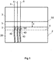
- the transfer process illustrated in figure 1 is a process for transferring a layer 1, comprising the following step:
- the transfer process illustrated in figure 1 comprises the following step: (b) forming a embrittlement region 4 in the donor substrate 2 so as to delimit a first part 1 and a second part 20 in the donor substrate 2 on either side of the embrittlement region 4, the first part 1 being intended to form the layer 1 to be transferred to the support substrate 3.
- the embrittlement region 4 is formed in step (b) by implanting species such as hydrogen and/or helium. It is possible to implant only a single species such as hydrogen, but also to implant a number of species, such as hydrogen and helium, sequentially.
- the implantation parameters, essentially dose and energy, are set depending on the nature of the species and of the donor substrate 2.
- the transfer process illustrated in figure 1 comprises the following step: (c) forming what is called a bonding layer 5 between the first part 1 of the donor substrate 2 and the support substrate 3, the bonding layer 5 having a preset thickness E.
- the bonding layer 5 may be a dielectric layer, preferably made from silicon dioxide or a nitride.
- the bonding layer may be formed on the first part 1 of the donor substrate 2 and/or on the support substrate 3, for example by thermal oxidation or by deposition.
- the bonding layer 5 is preferably silicon dioxide.
- the bonding layer 5 may therefore be produced on the support substrate 3, thereby replacing or complementing the bonding layer 5 formed on the donor substrate 2.
- step (b) is executed after step (c).
- step (b) is executed after step (c).
- step (c) when the bonding layer 5 is formed in step (c) by deposition, for example by low-temperature (about 250°C) chemical vapour deposition (CVD), then the thermal budget is sufficiently low for the donor substrate 2 not to be fractured in the embrittlement region 4, and step (b) may be executed before step (c).
- CVD chemical vapour deposition
- the transfer process illustrated in figure 1 comprises the following step: (d) assembling the donor substrate 2 to the support substrate 3. Step (d) may be executed by molecular bonding.
- the transfer process illustrated in figure 1 comprises the following step: (e) exposing, in succession, portions 40 of the embrittlement region 4 to electromagnetic irradiations 6 (symbolized by solid arrows) for an exposure time at a given power density.
- the electromagnetic irradiations 6 belong to a spectral domain chosen so that the support substrate 3, the bonding layer 5 and the donor substrate 2 are transparent, transparent and absorbent, respectively, in said spectral domain.
- the electromagnetic irradiations 6 absorbed in the donor substrate 2 are symbolized by wavelets 60.
- a first suitable spectral domain covers the following wavelength range: 0.3 ⁇ m - 0.5 ⁇ m.
- a second suitable spectral domain covers the following wavelength range: 1.5 ⁇ m - 2.5 ⁇ m provided that the silicon from which the donor substrate 2 is made is highly doped.
- the silicon may be highly p-doped, for example with a boron concentration higher than 5 ⁇ 10 18 atoms/cm 3 .
- the silicon may be highly n-doped, for example with an arsenic or phosphorus concentration higher than 5 ⁇ 10 18 atoms/cm 3 .
- These first and second spectral domains can also be used when the support substrate 3 is made of quartz.
- the length of time for which the portions 40 of the embrittlement region 4 are exposed to the electromagnetic irradiations 6 is chosen depending on the thickness E of the bonding layer 5 so that the temperature of the support substrate 3 remains below a threshold, during the exposure time, above which defects are liable to appear in the structure comprising the support substrate 3, the bonding layer 5 and the donor substrate 2. Furthermore, the exposure time is chosen depending on the power density in order to activate kinetics that weaken the embrittlement region 4.
- the electromagnetic irradiations 6 may be electromagnetic pulses, the length of each electromagnetic pulse respecting the following relationship: e ⁇ 2 D ⁇ ; where D is the thermal diffusion coefficient of the bonding layer 5, ⁇ is the length of one electromagnetic pulse, and e is the thickness of the bonding layer 5, ⁇ preferably being between 10 ns and 10 ⁇ s, and e preferably being lower than 10 ⁇ m.
- the number of periods and duty cycle of the electromagnetic pulses is chosen in order to activate kinetics that weaken the embrittlement region 4.
- a structure is considered in which:
- the thermal conductivity of the silicon-dioxide bonding layer 5 is about 1.4 W.m -1 .K -1 whereas the thermal conductivity of the silicon donor substrate 2 is about 148 W.m -1 .K -1 .
- step (e) When step (e) is executed under the above conditions, the temperature profile illustrated in figure 2 is obtained in the structure. Heat produced by absorption of the electromagnetic irradiations 6 by the layer 1 to be transferred diffuses:
- the temperature obtained for z ⁇ z 1 i.e. in the support substrate 3, is below a threshold (denoted T 0 in figure 2 ) above which defects are liable to appear in the structure comprising the support substrate 3, the bonding layer 5 and the donor substrate 2.
- the support substrate 3 is therefore sufficiently thermally decoupled from the first part 1 of the donor substrate 2.
- the exposure time may also be chosen depending on the power density in order to fracture the donor substrate 2 in the embrittlement region 4.
- the electromagnetic irradiations 6 raise each portion 40 of the embrittlement region 4 to a temperature below the melting point of the material from which the donor substrate 2 is made.
- the electromagnetic irradiations 6 raise each portion 40 of the embrittlement region 4 to a temperature preferably between 800°C and 1400°C, corresponding to the parameter T max in figure 2 , the melting point of silicon being substantially equal to 1415°C.
- Step (e) may be executed using at least one laser to emit the electromagnetic irradiations 6, said laser being scanned over the assembly so as to expose, in succession, the portions 40 of the embrittlement region 4.
- the laser may be a pulsed laser, for example a YAG laser tuned to 1.06 ⁇ m, and equipped with a frequency doubling or tripling system.
- the laser may also be an erbium fibre laser emitting at 1.5 ⁇ m.
- the laser may be a continuous wave laser, for example a dye laser allowing the wavelength to be chosen. In the case of a continuous wave laser, the laser beam is scanned so as to expose the portions 40 of the embrittlement region 4.
- Step (d) is executed at a temperature below a threshold above which defects are liable to appear in the support substrate 3 and the donor substrate 2, said temperature preferably being below 300°C and even more preferably below 200°C.
- the temperature at which step (d) is executed is chosen so that the support substrate 3 and the bonding layer 5 exhibit an interface 50 having a bonding energy such that they are reversibly assembled, said temperature preferably being below 250°C and even more preferably below 150°C.
- the transfer process comprises the following steps:
Landscapes
- Physics & Mathematics (AREA)
- Optics & Photonics (AREA)
- Recrystallisation Techniques (AREA)
- Ceramic Products (AREA)
- Thermal Transfer Or Thermal Recording In General (AREA)
- Electromagnetism (AREA)
- Heat Sensitive Colour Forming Recording (AREA)
Applications Claiming Priority (2)
| Application Number | Priority Date | Filing Date | Title |
|---|---|---|---|
| FR1201802A FR2992464B1 (fr) | 2012-06-26 | 2012-06-26 | Procede de transfert d'une couche |
| PCT/IB2013/001252 WO2014001869A1 (en) | 2012-06-26 | 2013-06-14 | Process for transferring a layer |
Publications (2)
| Publication Number | Publication Date |
|---|---|
| EP2865004A1 EP2865004A1 (en) | 2015-04-29 |
| EP2865004B1 true EP2865004B1 (en) | 2020-07-29 |
Family
ID=48782549
Family Applications (1)
| Application Number | Title | Priority Date | Filing Date |
|---|---|---|---|
| EP13735407.2A Active EP2865004B1 (en) | 2012-06-26 | 2013-06-14 | Process for transferring a layer |
Country Status (8)
| Country | Link |
|---|---|
| US (1) | US9343351B2 (enExample) |
| EP (1) | EP2865004B1 (enExample) |
| JP (1) | JP6138931B2 (enExample) |
| KR (1) | KR102007315B1 (enExample) |
| CN (1) | CN104584203B (enExample) |
| FR (1) | FR2992464B1 (enExample) |
| SG (1) | SG11201408606TA (enExample) |
| WO (1) | WO2014001869A1 (enExample) |
Families Citing this family (3)
| Publication number | Priority date | Publication date | Assignee | Title |
|---|---|---|---|---|
| FR3007892B1 (fr) * | 2013-06-27 | 2015-07-31 | Commissariat Energie Atomique | Procede de transfert d'une couche mince avec apport d'energie thermique a une zone fragilisee via une couche inductive |
| US9966466B2 (en) * | 2016-08-08 | 2018-05-08 | Globalfoundries Inc. | Semiconductor-on-insulator wafer, semiconductor structure including a transistor, and methods for the formation and operation thereof |
| CN108365083B (zh) * | 2018-02-07 | 2022-03-08 | 济南晶正电子科技有限公司 | 用于声表面波器件的复合压电衬底的制造方法 |
Family Cites Families (17)
| Publication number | Priority date | Publication date | Assignee | Title |
|---|---|---|---|---|
| EP1351308B1 (en) * | 1996-08-27 | 2009-04-22 | Seiko Epson Corporation | Exfoliating method and transferring method of thin film device |
| US6291314B1 (en) * | 1998-06-23 | 2001-09-18 | Silicon Genesis Corporation | Controlled cleavage process and device for patterned films using a release layer |
| TW452866B (en) * | 2000-02-25 | 2001-09-01 | Lee Tien Hsi | Manufacturing method of thin film on a substrate |
| FR2817394B1 (fr) * | 2000-11-27 | 2003-10-31 | Soitec Silicon On Insulator | Procede de fabrication d'un substrat notamment pour l'optique, l'electronique ou l'optoelectronique et substrat obtenu par ce procede |
| FR2855909B1 (fr) * | 2003-06-06 | 2005-08-26 | Soitec Silicon On Insulator | Procede d'obtention concomitante d'au moins une paire de structures comprenant au moins une couche utile reportee sur un substrat |
| US7052978B2 (en) * | 2003-08-28 | 2006-05-30 | Intel Corporation | Arrangements incorporating laser-induced cleaving |
| FR2860249B1 (fr) * | 2003-09-30 | 2005-12-09 | Michel Bruel | Procede de fabrication d'une structure en forme de plaque, en particulier en silicium, application de procede, et structure en forme de plaque, en particulier en silicium |
| US20060240275A1 (en) * | 2005-04-25 | 2006-10-26 | Gadkaree Kishor P | Flexible display substrates |
| DE102006007293B4 (de) * | 2006-01-31 | 2023-04-06 | OSRAM Opto Semiconductors Gesellschaft mit beschränkter Haftung | Verfahren zum Herstellen eines Quasi-Substratwafers und ein unter Verwendung eines solchen Quasi-Substratwafers hergestellter Halbleiterkörper |
| JP5284576B2 (ja) * | 2006-11-10 | 2013-09-11 | 信越化学工業株式会社 | 半導体基板の製造方法 |
| JP2008153411A (ja) * | 2006-12-18 | 2008-07-03 | Shin Etsu Chem Co Ltd | Soi基板の製造方法 |
| EP1986229A1 (en) * | 2007-04-27 | 2008-10-29 | S.O.I.T.E.C. Silicon on Insulator Technologies | Method for manufacturing compound material wafer and corresponding compound material wafer |
| US20090179160A1 (en) * | 2008-01-16 | 2009-07-16 | Semiconductor Energy Laboratory Co., Ltd. | Semiconductor substrate manufacturing apparatus |
| KR20100008123A (ko) * | 2008-07-15 | 2010-01-25 | 고려대학교 산학협력단 | 이중 히트 씽크층으로 구성된 지지대를 갖춘 고성능수직구조의 반도체 발광소자 |
| JP5496608B2 (ja) * | 2008-11-12 | 2014-05-21 | 信越化学工業株式会社 | Soi基板の作製方法 |
| JP5643509B2 (ja) * | 2009-12-28 | 2014-12-17 | 信越化学工業株式会社 | 応力を低減したsos基板の製造方法 |
| CN101866874B (zh) * | 2010-06-01 | 2013-05-22 | 中国科学院上海微系统与信息技术研究所 | 一种利用层转移技术制备绝缘体上锗硅材料的方法 |
-
2012
- 2012-06-26 FR FR1201802A patent/FR2992464B1/fr active Active
-
2013
- 2013-06-14 KR KR1020147036692A patent/KR102007315B1/ko active Active
- 2013-06-14 JP JP2015519373A patent/JP6138931B2/ja active Active
- 2013-06-14 WO PCT/IB2013/001252 patent/WO2014001869A1/en not_active Ceased
- 2013-06-14 CN CN201380033314.5A patent/CN104584203B/zh active Active
- 2013-06-14 EP EP13735407.2A patent/EP2865004B1/en active Active
- 2013-06-14 SG SG11201408606TA patent/SG11201408606TA/en unknown
- 2013-06-14 US US14/409,361 patent/US9343351B2/en active Active
Non-Patent Citations (1)
| Title |
|---|
| None * |
Also Published As
| Publication number | Publication date |
|---|---|
| JP6138931B2 (ja) | 2017-05-31 |
| CN104584203B (zh) | 2018-03-20 |
| EP2865004A1 (en) | 2015-04-29 |
| WO2014001869A1 (en) | 2014-01-03 |
| CN104584203A (zh) | 2015-04-29 |
| US20150187638A1 (en) | 2015-07-02 |
| JP2015525964A (ja) | 2015-09-07 |
| FR2992464A1 (fr) | 2013-12-27 |
| FR2992464B1 (fr) | 2015-04-03 |
| KR20150023514A (ko) | 2015-03-05 |
| SG11201408606TA (en) | 2015-01-29 |
| KR102007315B1 (ko) | 2019-08-06 |
| US9343351B2 (en) | 2016-05-17 |
Similar Documents
| Publication | Publication Date | Title |
|---|---|---|
| US8993461B2 (en) | Method for curing defects in a semiconductor layer | |
| US6486008B1 (en) | Manufacturing method of a thin film on a substrate | |
| AU2009325425B2 (en) | Method for manufacturing composite substrate on which wide bandgap semiconductor is laminated | |
| JP5214160B2 (ja) | 薄膜を製造する方法 | |
| EP2169730A2 (en) | Layer transfer of films utilizing controlled propagation | |
| EP2511942A1 (en) | Method for manufacturing semiconductor device, and semiconductor device | |
| US9343351B2 (en) | Process for transferring a layer | |
| KR101698912B1 (ko) | 삼중 주입을 사용하는, 클리빙에 의해 실리콘 박막을 분리하는 방법 | |
| US11508613B2 (en) | Method of healing an implanted layer comprising a heat treatment prior to recrystallisation by laser annealing | |
| CN101855709B (zh) | 通过光通量加热晶片的方法 | |
| US20200219719A1 (en) | Healing method before transfer of a semiconducting layer | |
| US20040058501A1 (en) | Apparatus and method for adiabatically heating a semiconductor surface | |
| US20220293414A1 (en) | Method for modifying a strain state of at least one semiconductor layer | |
| CN116391264A (zh) | 用于将结构从基底分离的方法 | |
| US9564496B2 (en) | Process for treating a substrate using a luminous flux of determined wavelength, and corresponding substrate | |
| JP2010287817A (ja) | Ge膜付きSOI基板の製造方法及びGe膜付きSOI基板 | |
| Setsuhara et al. | Nano-surface modification of silicon with ultra-short pulse laser process |
Legal Events
| Date | Code | Title | Description |
|---|---|---|---|
| PUAI | Public reference made under article 153(3) epc to a published international application that has entered the european phase |
Free format text: ORIGINAL CODE: 0009012 |
|
| 17P | Request for examination filed |
Effective date: 20141212 |
|
| AK | Designated contracting states |
Kind code of ref document: A1 Designated state(s): AL AT BE BG CH CY CZ DE DK EE ES FI FR GB GR HR HU IE IS IT LI LT LU LV MC MK MT NL NO PL PT RO RS SE SI SK SM TR |
|
| AX | Request for extension of the european patent |
Extension state: BA ME |
|
| DAX | Request for extension of the european patent (deleted) | ||
| GRAP | Despatch of communication of intention to grant a patent |
Free format text: ORIGINAL CODE: EPIDOSNIGR1 |
|
| STAA | Information on the status of an ep patent application or granted ep patent |
Free format text: STATUS: GRANT OF PATENT IS INTENDED |
|
| INTG | Intention to grant announced |
Effective date: 20190923 |
|
| GRAJ | Information related to disapproval of communication of intention to grant by the applicant or resumption of examination proceedings by the epo deleted |
Free format text: ORIGINAL CODE: EPIDOSDIGR1 |
|
| STAA | Information on the status of an ep patent application or granted ep patent |
Free format text: STATUS: REQUEST FOR EXAMINATION WAS MADE |
|
| GRAP | Despatch of communication of intention to grant a patent |
Free format text: ORIGINAL CODE: EPIDOSNIGR1 |
|
| STAA | Information on the status of an ep patent application or granted ep patent |
Free format text: STATUS: GRANT OF PATENT IS INTENDED |
|
| INTC | Intention to grant announced (deleted) | ||
| INTG | Intention to grant announced |
Effective date: 20200318 |
|
| GRAS | Grant fee paid |
Free format text: ORIGINAL CODE: EPIDOSNIGR3 |
|
| GRAA | (expected) grant |
Free format text: ORIGINAL CODE: 0009210 |
|
| STAA | Information on the status of an ep patent application or granted ep patent |
Free format text: STATUS: THE PATENT HAS BEEN GRANTED |
|
| AK | Designated contracting states |
Kind code of ref document: B1 Designated state(s): AL AT BE BG CH CY CZ DE DK EE ES FI FR GB GR HR HU IE IS IT LI LT LU LV MC MK MT NL NO PL PT RO RS SE SI SK SM TR |
|
| REG | Reference to a national code |
Ref country code: GB Ref legal event code: FG4D |
|
| REG | Reference to a national code |
Ref country code: CH Ref legal event code: EP |
|
| REG | Reference to a national code |
Ref country code: DE Ref legal event code: R096 Ref document number: 602013071113 Country of ref document: DE |
|
| REG | Reference to a national code |
Ref country code: AT Ref legal event code: REF Ref document number: 1296795 Country of ref document: AT Kind code of ref document: T Effective date: 20200815 |
|
| REG | Reference to a national code |
Ref country code: IE Ref legal event code: FG4D |
|
| REG | Reference to a national code |
Ref country code: SE Ref legal event code: TRGR |
|
| REG | Reference to a national code |
Ref country code: NL Ref legal event code: FP |
|
| REG | Reference to a national code |
Ref country code: FI Ref legal event code: FGE |
|
| REG | Reference to a national code |
Ref country code: LT Ref legal event code: MG4D |
|
| REG | Reference to a national code |
Ref country code: AT Ref legal event code: MK05 Ref document number: 1296795 Country of ref document: AT Kind code of ref document: T Effective date: 20200729 |
|
| PG25 | Lapsed in a contracting state [announced via postgrant information from national office to epo] |
Ref country code: PT Free format text: LAPSE BECAUSE OF FAILURE TO SUBMIT A TRANSLATION OF THE DESCRIPTION OR TO PAY THE FEE WITHIN THE PRESCRIBED TIME-LIMIT Effective date: 20201130 Ref country code: BG Free format text: LAPSE BECAUSE OF FAILURE TO SUBMIT A TRANSLATION OF THE DESCRIPTION OR TO PAY THE FEE WITHIN THE PRESCRIBED TIME-LIMIT Effective date: 20201029 Ref country code: ES Free format text: LAPSE BECAUSE OF FAILURE TO SUBMIT A TRANSLATION OF THE DESCRIPTION OR TO PAY THE FEE WITHIN THE PRESCRIBED TIME-LIMIT Effective date: 20200729 Ref country code: NO Free format text: LAPSE BECAUSE OF FAILURE TO SUBMIT A TRANSLATION OF THE DESCRIPTION OR TO PAY THE FEE WITHIN THE PRESCRIBED TIME-LIMIT Effective date: 20201029 Ref country code: AT Free format text: LAPSE BECAUSE OF FAILURE TO SUBMIT A TRANSLATION OF THE DESCRIPTION OR TO PAY THE FEE WITHIN THE PRESCRIBED TIME-LIMIT Effective date: 20200729 Ref country code: LT Free format text: LAPSE BECAUSE OF FAILURE TO SUBMIT A TRANSLATION OF THE DESCRIPTION OR TO PAY THE FEE WITHIN THE PRESCRIBED TIME-LIMIT Effective date: 20200729 Ref country code: HR Free format text: LAPSE BECAUSE OF FAILURE TO SUBMIT A TRANSLATION OF THE DESCRIPTION OR TO PAY THE FEE WITHIN THE PRESCRIBED TIME-LIMIT Effective date: 20200729 |
|
| PG25 | Lapsed in a contracting state [announced via postgrant information from national office to epo] |
Ref country code: IS Free format text: LAPSE BECAUSE OF FAILURE TO SUBMIT A TRANSLATION OF THE DESCRIPTION OR TO PAY THE FEE WITHIN THE PRESCRIBED TIME-LIMIT Effective date: 20201129 Ref country code: RS Free format text: LAPSE BECAUSE OF FAILURE TO SUBMIT A TRANSLATION OF THE DESCRIPTION OR TO PAY THE FEE WITHIN THE PRESCRIBED TIME-LIMIT Effective date: 20200729 Ref country code: PL Free format text: LAPSE BECAUSE OF FAILURE TO SUBMIT A TRANSLATION OF THE DESCRIPTION OR TO PAY THE FEE WITHIN THE PRESCRIBED TIME-LIMIT Effective date: 20200729 Ref country code: LV Free format text: LAPSE BECAUSE OF FAILURE TO SUBMIT A TRANSLATION OF THE DESCRIPTION OR TO PAY THE FEE WITHIN THE PRESCRIBED TIME-LIMIT Effective date: 20200729 |
|
| PG25 | Lapsed in a contracting state [announced via postgrant information from national office to epo] |
Ref country code: CZ Free format text: LAPSE BECAUSE OF FAILURE TO SUBMIT A TRANSLATION OF THE DESCRIPTION OR TO PAY THE FEE WITHIN THE PRESCRIBED TIME-LIMIT Effective date: 20200729 Ref country code: EE Free format text: LAPSE BECAUSE OF FAILURE TO SUBMIT A TRANSLATION OF THE DESCRIPTION OR TO PAY THE FEE WITHIN THE PRESCRIBED TIME-LIMIT Effective date: 20200729 Ref country code: DK Free format text: LAPSE BECAUSE OF FAILURE TO SUBMIT A TRANSLATION OF THE DESCRIPTION OR TO PAY THE FEE WITHIN THE PRESCRIBED TIME-LIMIT Effective date: 20200729 Ref country code: SM Free format text: LAPSE BECAUSE OF FAILURE TO SUBMIT A TRANSLATION OF THE DESCRIPTION OR TO PAY THE FEE WITHIN THE PRESCRIBED TIME-LIMIT Effective date: 20200729 Ref country code: RO Free format text: LAPSE BECAUSE OF FAILURE TO SUBMIT A TRANSLATION OF THE DESCRIPTION OR TO PAY THE FEE WITHIN THE PRESCRIBED TIME-LIMIT Effective date: 20200729 |
|
| REG | Reference to a national code |
Ref country code: DE Ref legal event code: R097 Ref document number: 602013071113 Country of ref document: DE |
|
| PG25 | Lapsed in a contracting state [announced via postgrant information from national office to epo] |
Ref country code: AL Free format text: LAPSE BECAUSE OF FAILURE TO SUBMIT A TRANSLATION OF THE DESCRIPTION OR TO PAY THE FEE WITHIN THE PRESCRIBED TIME-LIMIT Effective date: 20200729 |
|
| PLBE | No opposition filed within time limit |
Free format text: ORIGINAL CODE: 0009261 |
|
| STAA | Information on the status of an ep patent application or granted ep patent |
Free format text: STATUS: NO OPPOSITION FILED WITHIN TIME LIMIT |
|
| PG25 | Lapsed in a contracting state [announced via postgrant information from national office to epo] |
Ref country code: SK Free format text: LAPSE BECAUSE OF FAILURE TO SUBMIT A TRANSLATION OF THE DESCRIPTION OR TO PAY THE FEE WITHIN THE PRESCRIBED TIME-LIMIT Effective date: 20200729 |
|
| 26N | No opposition filed |
Effective date: 20210430 |
|
| PG25 | Lapsed in a contracting state [announced via postgrant information from national office to epo] |
Ref country code: SI Free format text: LAPSE BECAUSE OF FAILURE TO SUBMIT A TRANSLATION OF THE DESCRIPTION OR TO PAY THE FEE WITHIN THE PRESCRIBED TIME-LIMIT Effective date: 20200729 |
|
| PG25 | Lapsed in a contracting state [announced via postgrant information from national office to epo] |
Ref country code: MC Free format text: LAPSE BECAUSE OF FAILURE TO SUBMIT A TRANSLATION OF THE DESCRIPTION OR TO PAY THE FEE WITHIN THE PRESCRIBED TIME-LIMIT Effective date: 20200729 |
|
| REG | Reference to a national code |
Ref country code: CH Ref legal event code: PL |
|
| GBPC | Gb: european patent ceased through non-payment of renewal fee |
Effective date: 20210614 |
|
| REG | Reference to a national code |
Ref country code: BE Ref legal event code: MM Effective date: 20210630 |
|
| PG25 | Lapsed in a contracting state [announced via postgrant information from national office to epo] |
Ref country code: LU Free format text: LAPSE BECAUSE OF NON-PAYMENT OF DUE FEES Effective date: 20210614 |
|
| PG25 | Lapsed in a contracting state [announced via postgrant information from national office to epo] |
Ref country code: LI Free format text: LAPSE BECAUSE OF NON-PAYMENT OF DUE FEES Effective date: 20210630 Ref country code: IE Free format text: LAPSE BECAUSE OF NON-PAYMENT OF DUE FEES Effective date: 20210614 Ref country code: GB Free format text: LAPSE BECAUSE OF NON-PAYMENT OF DUE FEES Effective date: 20210614 Ref country code: CH Free format text: LAPSE BECAUSE OF NON-PAYMENT OF DUE FEES Effective date: 20210630 |
|
| PG25 | Lapsed in a contracting state [announced via postgrant information from national office to epo] |
Ref country code: BE Free format text: LAPSE BECAUSE OF NON-PAYMENT OF DUE FEES Effective date: 20210630 |
|
| PG25 | Lapsed in a contracting state [announced via postgrant information from national office to epo] |
Ref country code: HU Free format text: LAPSE BECAUSE OF FAILURE TO SUBMIT A TRANSLATION OF THE DESCRIPTION OR TO PAY THE FEE WITHIN THE PRESCRIBED TIME-LIMIT; INVALID AB INITIO Effective date: 20130614 |
|
| PG25 | Lapsed in a contracting state [announced via postgrant information from national office to epo] |
Ref country code: CY Free format text: LAPSE BECAUSE OF FAILURE TO SUBMIT A TRANSLATION OF THE DESCRIPTION OR TO PAY THE FEE WITHIN THE PRESCRIBED TIME-LIMIT Effective date: 20200729 |
|
| PG25 | Lapsed in a contracting state [announced via postgrant information from national office to epo] |
Ref country code: GR Free format text: LAPSE BECAUSE OF FAILURE TO SUBMIT A TRANSLATION OF THE DESCRIPTION OR TO PAY THE FEE WITHIN THE PRESCRIBED TIME-LIMIT Effective date: 20200729 |
|
| PG25 | Lapsed in a contracting state [announced via postgrant information from national office to epo] |
Ref country code: MK Free format text: LAPSE BECAUSE OF FAILURE TO SUBMIT A TRANSLATION OF THE DESCRIPTION OR TO PAY THE FEE WITHIN THE PRESCRIBED TIME-LIMIT Effective date: 20200729 |
|
| PG25 | Lapsed in a contracting state [announced via postgrant information from national office to epo] |
Ref country code: MT Free format text: LAPSE BECAUSE OF FAILURE TO SUBMIT A TRANSLATION OF THE DESCRIPTION OR TO PAY THE FEE WITHIN THE PRESCRIBED TIME-LIMIT Effective date: 20200729 |
|
| PGFP | Annual fee paid to national office [announced via postgrant information from national office to epo] |
Ref country code: NL Payment date: 20250516 Year of fee payment: 13 |
|
| PGFP | Annual fee paid to national office [announced via postgrant information from national office to epo] |
Ref country code: FI Payment date: 20250620 Year of fee payment: 13 |
|
| PGFP | Annual fee paid to national office [announced via postgrant information from national office to epo] |
Ref country code: DE Payment date: 20250507 Year of fee payment: 13 |
|
| PGFP | Annual fee paid to national office [announced via postgrant information from national office to epo] |
Ref country code: IT Payment date: 20250522 Year of fee payment: 13 |
|
| PGFP | Annual fee paid to national office [announced via postgrant information from national office to epo] |
Ref country code: FR Payment date: 20250523 Year of fee payment: 13 |
|
| PGFP | Annual fee paid to national office [announced via postgrant information from national office to epo] |
Ref country code: SE Payment date: 20250514 Year of fee payment: 13 |
|
| REG | Reference to a national code |
Ref country code: DE Ref legal event code: R079 Ref document number: 602013071113 Country of ref document: DE Free format text: PREVIOUS MAIN CLASS: H01L0021762000 Ipc: H10W0010100000 |
|
| PG25 | Lapsed in a contracting state [announced via postgrant information from national office to epo] |
Ref country code: TR Free format text: LAPSE BECAUSE OF FAILURE TO SUBMIT A TRANSLATION OF THE DESCRIPTION OR TO PAY THE FEE WITHIN THE PRESCRIBED TIME-LIMIT Effective date: 20200729 |