EP2864130B2 - Dekorelement, sicherheitsdokument mit einem dekorelement sowie verfahren zur herstellung eines dekorelements - Google Patents
Dekorelement, sicherheitsdokument mit einem dekorelement sowie verfahren zur herstellung eines dekorelements Download PDFInfo
- Publication number
- EP2864130B2 EP2864130B2 EP13731331.8A EP13731331A EP2864130B2 EP 2864130 B2 EP2864130 B2 EP 2864130B2 EP 13731331 A EP13731331 A EP 13731331A EP 2864130 B2 EP2864130 B2 EP 2864130B2
- Authority
- EP
- European Patent Office
- Prior art keywords
- base
- basic elements
- region
- light
- color
- Prior art date
- Legal status (The legal status is an assumption and is not a legal conclusion. Google has not performed a legal analysis and makes no representation as to the accuracy of the status listed.)
- Active
Links
Images


Classifications
-
- G—PHYSICS
- G03—PHOTOGRAPHY; CINEMATOGRAPHY; ANALOGOUS TECHNIQUES USING WAVES OTHER THAN OPTICAL WAVES; ELECTROGRAPHY; HOLOGRAPHY
- G03H—HOLOGRAPHIC PROCESSES OR APPARATUS
- G03H1/00—Holographic processes or apparatus using light, infrared or ultraviolet waves for obtaining holograms or for obtaining an image from them; Details peculiar thereto
- G03H1/0005—Adaptation of holography to specific applications
- G03H1/0011—Adaptation of holography to specific applications for security or authentication
-
- B—PERFORMING OPERATIONS; TRANSPORTING
- B42—BOOKBINDING; ALBUMS; FILES; SPECIAL PRINTED MATTER
- B42D—BOOKS; BOOK COVERS; LOOSE LEAVES; PRINTED MATTER CHARACTERISED BY IDENTIFICATION OR SECURITY FEATURES; PRINTED MATTER OF SPECIAL FORMAT OR STYLE NOT OTHERWISE PROVIDED FOR; DEVICES FOR USE THEREWITH AND NOT OTHERWISE PROVIDED FOR; MOVABLE-STRIP WRITING OR READING APPARATUS
- B42D25/00—Information-bearing cards or sheet-like structures characterised by identification or security features; Manufacture thereof
- B42D25/20—Information-bearing cards or sheet-like structures characterised by identification or security features; Manufacture thereof characterised by a particular use or purpose
- B42D25/21—Information-bearing cards or sheet-like structures characterised by identification or security features; Manufacture thereof characterised by a particular use or purpose for multiple purposes
-
- B—PERFORMING OPERATIONS; TRANSPORTING
- B42—BOOKBINDING; ALBUMS; FILES; SPECIAL PRINTED MATTER
- B42D—BOOKS; BOOK COVERS; LOOSE LEAVES; PRINTED MATTER CHARACTERISED BY IDENTIFICATION OR SECURITY FEATURES; PRINTED MATTER OF SPECIAL FORMAT OR STYLE NOT OTHERWISE PROVIDED FOR; DEVICES FOR USE THEREWITH AND NOT OTHERWISE PROVIDED FOR; MOVABLE-STRIP WRITING OR READING APPARATUS
- B42D25/00—Information-bearing cards or sheet-like structures characterised by identification or security features; Manufacture thereof
- B42D25/30—Identification or security features, e.g. for preventing forgery
- B42D25/346—Perforations
-
- B—PERFORMING OPERATIONS; TRANSPORTING
- B42—BOOKBINDING; ALBUMS; FILES; SPECIAL PRINTED MATTER
- B42D—BOOKS; BOOK COVERS; LOOSE LEAVES; PRINTED MATTER CHARACTERISED BY IDENTIFICATION OR SECURITY FEATURES; PRINTED MATTER OF SPECIAL FORMAT OR STYLE NOT OTHERWISE PROVIDED FOR; DEVICES FOR USE THEREWITH AND NOT OTHERWISE PROVIDED FOR; MOVABLE-STRIP WRITING OR READING APPARATUS
- B42D25/00—Information-bearing cards or sheet-like structures characterised by identification or security features; Manufacture thereof
- B42D25/30—Identification or security features, e.g. for preventing forgery
- B42D25/351—Translucent or partly translucent parts, e.g. windows
-
- B—PERFORMING OPERATIONS; TRANSPORTING
- B42—BOOKBINDING; ALBUMS; FILES; SPECIAL PRINTED MATTER
- B42D—BOOKS; BOOK COVERS; LOOSE LEAVES; PRINTED MATTER CHARACTERISED BY IDENTIFICATION OR SECURITY FEATURES; PRINTED MATTER OF SPECIAL FORMAT OR STYLE NOT OTHERWISE PROVIDED FOR; DEVICES FOR USE THEREWITH AND NOT OTHERWISE PROVIDED FOR; MOVABLE-STRIP WRITING OR READING APPARATUS
- B42D25/00—Information-bearing cards or sheet-like structures characterised by identification or security features; Manufacture thereof
- B42D25/30—Identification or security features, e.g. for preventing forgery
- B42D25/355—Security threads
-
- B—PERFORMING OPERATIONS; TRANSPORTING
- B42—BOOKBINDING; ALBUMS; FILES; SPECIAL PRINTED MATTER
- B42D—BOOKS; BOOK COVERS; LOOSE LEAVES; PRINTED MATTER CHARACTERISED BY IDENTIFICATION OR SECURITY FEATURES; PRINTED MATTER OF SPECIAL FORMAT OR STYLE NOT OTHERWISE PROVIDED FOR; DEVICES FOR USE THEREWITH AND NOT OTHERWISE PROVIDED FOR; MOVABLE-STRIP WRITING OR READING APPARATUS
- B42D25/00—Information-bearing cards or sheet-like structures characterised by identification or security features; Manufacture thereof
- B42D25/30—Identification or security features, e.g. for preventing forgery
- B42D25/36—Identification or security features, e.g. for preventing forgery comprising special materials
- B42D25/373—Metallic materials
-
- B—PERFORMING OPERATIONS; TRANSPORTING
- B42—BOOKBINDING; ALBUMS; FILES; SPECIAL PRINTED MATTER
- B42D—BOOKS; BOOK COVERS; LOOSE LEAVES; PRINTED MATTER CHARACTERISED BY IDENTIFICATION OR SECURITY FEATURES; PRINTED MATTER OF SPECIAL FORMAT OR STYLE NOT OTHERWISE PROVIDED FOR; DEVICES FOR USE THEREWITH AND NOT OTHERWISE PROVIDED FOR; MOVABLE-STRIP WRITING OR READING APPARATUS
- B42D25/00—Information-bearing cards or sheet-like structures characterised by identification or security features; Manufacture thereof
- B42D25/30—Identification or security features, e.g. for preventing forgery
- B42D25/36—Identification or security features, e.g. for preventing forgery comprising special materials
- B42D25/378—Special inks
-
- B—PERFORMING OPERATIONS; TRANSPORTING
- B44—DECORATIVE ARTS
- B44C—PRODUCING DECORATIVE EFFECTS; MOSAICS; TARSIA WORK; PAPERHANGING
- B44C1/00—Processes, not specifically provided for elsewhere, for producing decorative surface effects
- B44C1/16—Processes, not specifically provided for elsewhere, for producing decorative surface effects for applying transfer pictures or the like
- B44C1/165—Processes, not specifically provided for elsewhere, for producing decorative surface effects for applying transfer pictures or the like for decalcomanias; sheet material therefor
- B44C1/17—Dry transfer
- B44C1/1712—Decalcomanias applied under heat and pressure, e.g. provided with a heat activable adhesive
- B44C1/1729—Hot stamping techniques
-
- B—PERFORMING OPERATIONS; TRANSPORTING
- B44—DECORATIVE ARTS
- B44F—SPECIAL DESIGNS OR PICTURES
- B44F1/00—Designs or pictures characterised by special or unusual light effects
- B44F1/08—Designs or pictures characterised by special or unusual light effects characterised by colour effects
- B44F1/14—Iridescent effects
-
- G—PHYSICS
- G02—OPTICS
- G02B—OPTICAL ELEMENTS, SYSTEMS OR APPARATUS
- G02B1/00—Optical elements characterised by the material of which they are made; Optical coatings for optical elements
- G02B1/10—Optical coatings produced by application to, or surface treatment of, optical elements
- G02B1/14—Protective coatings, e.g. hard coatings
-
- G—PHYSICS
- G02—OPTICS
- G02B—OPTICAL ELEMENTS, SYSTEMS OR APPARATUS
- G02B5/00—Optical elements other than lenses
- G02B5/18—Diffraction gratings
-
- G—PHYSICS
- G02—OPTICS
- G02B—OPTICAL ELEMENTS, SYSTEMS OR APPARATUS
- G02B5/00—Optical elements other than lenses
- G02B5/18—Diffraction gratings
- G02B5/1809—Diffraction gratings with pitch less than or comparable to the wavelength
-
- G—PHYSICS
- G02—OPTICS
- G02B—OPTICAL ELEMENTS, SYSTEMS OR APPARATUS
- G02B5/00—Optical elements other than lenses
- G02B5/20—Filters
- G02B5/28—Interference filters
- G02B5/285—Interference filters comprising deposited thin solid films
-
- G—PHYSICS
- G03—PHOTOGRAPHY; CINEMATOGRAPHY; ANALOGOUS TECHNIQUES USING WAVES OTHER THAN OPTICAL WAVES; ELECTROGRAPHY; HOLOGRAPHY
- G03H—HOLOGRAPHIC PROCESSES OR APPARATUS
- G03H1/00—Holographic processes or apparatus using light, infrared or ultraviolet waves for obtaining holograms or for obtaining an image from them; Details peculiar thereto
- G03H1/02—Details of features involved during the holographic process; Replication of holograms without interference recording
- G03H1/024—Hologram nature or properties
- G03H1/0244—Surface relief holograms
-
- B—PERFORMING OPERATIONS; TRANSPORTING
- B42—BOOKBINDING; ALBUMS; FILES; SPECIAL PRINTED MATTER
- B42D—BOOKS; BOOK COVERS; LOOSE LEAVES; PRINTED MATTER CHARACTERISED BY IDENTIFICATION OR SECURITY FEATURES; PRINTED MATTER OF SPECIAL FORMAT OR STYLE NOT OTHERWISE PROVIDED FOR; DEVICES FOR USE THEREWITH AND NOT OTHERWISE PROVIDED FOR; MOVABLE-STRIP WRITING OR READING APPARATUS
- B42D25/00—Information-bearing cards or sheet-like structures characterised by identification or security features; Manufacture thereof
- B42D25/30—Identification or security features, e.g. for preventing forgery
- B42D25/324—Reliefs
-
- B—PERFORMING OPERATIONS; TRANSPORTING
- B42—BOOKBINDING; ALBUMS; FILES; SPECIAL PRINTED MATTER
- B42D—BOOKS; BOOK COVERS; LOOSE LEAVES; PRINTED MATTER CHARACTERISED BY IDENTIFICATION OR SECURITY FEATURES; PRINTED MATTER OF SPECIAL FORMAT OR STYLE NOT OTHERWISE PROVIDED FOR; DEVICES FOR USE THEREWITH AND NOT OTHERWISE PROVIDED FOR; MOVABLE-STRIP WRITING OR READING APPARATUS
- B42D25/00—Information-bearing cards or sheet-like structures characterised by identification or security features; Manufacture thereof
- B42D25/30—Identification or security features, e.g. for preventing forgery
- B42D25/328—Diffraction gratings; Holograms
-
- G—PHYSICS
- G09—EDUCATION; CRYPTOGRAPHY; DISPLAY; ADVERTISING; SEALS
- G09F—DISPLAYING; ADVERTISING; SIGNS; LABELS OR NAME-PLATES; SEALS
- G09F3/00—Labels, tag tickets, or similar identification or indication means; Seals; Postage or like stamps
- G09F3/02—Forms or constructions
- G09F2003/0276—Safety features, e.g. colour, prominent part, logo
Definitions
- the invention relates to a decorative element, in particular in the form of a transfer film, a laminating film or a security thread, as well as a security document and a method for producing such a decorative element.
- microstructures in security documents that show a rainbow-shaped color gradient when tilted.
- Holograms are the most well-known example of this.
- the color gradient is generated due to the wavelength-dependent diffraction of light into the first and higher diffraction orders.
- the color gradient is therefore not visible in the zeroth diffraction order, for example when viewing the security document in reflection in a mirror reflex, but only when tilted from the zeroth diffraction order in a tilt angle range that corresponds to the first or higher diffraction orders.
- the DE 10 2010 050 031 A1 describes a security element with a pattern area consisting of a design element that provides optically perceptible information.
- the pattern area is surrounded by a background area, with zones of the pattern area having an opaque reflective layer.
- the EP 2 264 491 A1 discloses a method for producing a zero-order diffraction grating consisting of three layers by means of a wet paint process, wherein the middle layer comprises a material with a higher refractive index than the surrounding layers.
- the DE 10 2011 014 114 B3 describes a multilayer body in whose surface a plurality of facet surfaces are molded and which have dimensions between 1 ⁇ m and 300 ⁇ m, wherein one or more of the parameters of the facet surfaces are varied pseudo-randomly and a reflective layer is applied to each of the facet surfaces.
- the EP 2 077 459 A1 relates to a display that has two areas with different diffraction structures.
- the first area is formed by a surface structure that corresponds to a line grating.
- the second area is formed by a structure that is characterized by a smaller period compared to the first area and is formed by depressions or projections.
- the WO2007/131375 A1 discloses the preamble of claim 1 and describes an element having at least one surface region with an optically effective surface relief microstructure (12), wherein the surface relief microstructure has a surface modulation of transitions from upper regions (13) to lower regions (14) and from lower regions (14) to upper regions (13).
- the invention is based on the object of specifying a decorative element and a method for producing a decorative element which is characterized by memorable color effects.
- This object is further achieved by a method for producing a decorative element according to claim 6.
- the generation of the first colour in the scattered light represents a solution not according to the invention.
- the microstructure is preferably coated with a reflection-enhancing layer, in particular with a layer of metal or a highly refractive material, e.g. with aluminum or zinc sulfide (ZnS).
- a reflection-enhancing layer in particular with a layer of metal or a highly refractive material, e.g. with aluminum or zinc sulfide (ZnS).
- high refractive index means a material with a refractive index in the visible spectral range (typically at a wavelength of approx. 635 nm) of more than 1.7.
- Examples of such high refractive index first materials are listed in Table 1. The numerical values are only rough guidelines, since the actual refractive index of a layer depends on many parameters such as crystal structure, porosity, etc.
- Table 1 material molecular formula refractive index n lead sulfide PbS 4.33 zinc telluride ZnTe 3.04 silicon carbide SiC 2.64 iron oxide Fe 2 O 3 2.92 barium titanate BaTiO 3 2.41 Titanium dioxide (refractive index depends on the crystal structure) TiO 2 > 2.4 zinc sulfide ZnS 2.35 niobdenum oxide Nd 2 O 5 2.32 zirconium oxide ZrO 2 2.21 tantalum pentoxide Ta 2 O 5 2.2 zinc oxide ZnO 2.1 silicon nitride Si 3 O 4 2.02 indium oxide In 2 O 3 2.0 silicon monoxide SiO 1.97 hafnium oxide HfO 2 1.91 yttrium oxide Y 2 O 3 1.9 aluminum oxide nitride AlON 1.79 magnesium oxide MgO 1.74
- diffractive microstructures e.g. diffraction gratings or scattering microstructures
- diffractive microstructures e.g. diffraction gratings or scattering microstructures
- the interactions of such microstructures are completely described in an exact manner by the exact electromagnetic theory in the form of the Maxwell equations and the corresponding boundary conditions, i.e. diffraction efficiencies, wave fronts, electromagnetic field or intensity distributions can be calculated if the respective systems are sufficiently known.
- this exact approach is generally not very helpful in understanding, which is why phenomenological descriptions are often used in addition within certain models.
- the Huygens principle for propagation (named after the Dutch physicist Christiaan Huygens) and Fresnel interference (named after the French physicist Augustin-Jean Fresnel).
- the grating diffraction that occurs at periodic microstructures is a special type of diffraction and can be understood phenomenologically as a combination of Huygens propagation and Fresnel interference.
- the first distance is preferably selected such that a color is generated, in particular the first color or the second color, by interference of the light reflected at the base surface and the element surfaces in the zeroth diffraction order in incident light and/or by interference of the light transmitted through the element surfaces and the base surface in the zeroth diffraction order in transmitted light.
- the ratio of the surface area of the base elements compared to the surface area of the base surface determines the efficiency with which the light rays with the different path lengths interfere. This ratio therefore also determines the strength of the color or the color impression.
- the zeroth diffraction order corresponds to direct reflection or direct transmission.
- Direct reflection is evident, for example, in the mirror reflection of a light source.
- the first distance is preferably set to achieve the respective desired first color when viewed in the first or a higher diffraction order or in scattered light.
- the first distance for effects in reflection is selected between 150 nm and 1000 nm and more preferably between 200 nm and 600 nm.
- the first distance is preferably selected between 300 nm and 4000 nm and more preferably between 400 nm and 2000 nm. The distance to be set depends on the refractive index of the material that is located between the two levels.
- This distance preferably varies in a region with a uniform color impression by less than +/- 50 nm, more preferably less than +/- 20 nm, even more preferably less than +/- 10 nm.
- the base area and the element surfaces are thus preferably arranged parallel to one another in such a way that the first distance or the second, third or fourth distance do not vary by more than +/- 50 nm, preferably less than +/- 20 nm, more preferably less than +/- 10 nm, in particular in the first region.
- complementary refers to the color-psychological aspect.
- Colour is further preferably understood to mean a change in the spectrum of the incident or transmitted light in the visible wavelength range, for example a red or blue colour impression with a white light source.
- the desired color impression that is relevant for the visual effect and more striking is preferably the first color impression.
- the color impressions described above occur particularly strongly when at least one lateral extension of the projections of the basic elements onto the ground plane is between 0.25 and 50 ⁇ m, preferably between 0.4 ⁇ m and 20 ⁇ m and more preferably between 0.75 ⁇ m and 10 ⁇ m, in particular all lateral extensions of the projection of each basic element onto the ground plane fulfill this condition.
- the projection of a basic element onto the ground plane is understood to mean the area occupied by the basic element when the basic element is viewed perpendicular to the ground plane.
- the minimum distance between adjacent basic elements is no greater than 500 ⁇ m, in particular between 0.2 ⁇ m and 300 ⁇ m, more preferably between 0.4 ⁇ m and 50 ⁇ m. It has been shown that with such a choice of this parameter, the color impressions described above are particularly strong.
- the spacing of adjacent basic elements is the distance between adjacent basic elements in the base plane, ie the spacing of the projections of adjacent basic elements onto the base plane.
- the minimum spacing of adjacent basic elements thus represents the minimum spacing of the projection of adjacent basic elements onto the base plane, ie the minimum spacing resulting from a top view perpendicular to the base plane. Spacing of adjacent basic elements.
- the average surface coverage of the base plane with the basic elements in the first area or in a partial area of the first area is selected to be between 30% and 70%, more preferably between 40% and 60% and particularly preferably around 50%. It has been shown that the color impressions described above are particularly pronounced with such a selection of surface coverage.
- the average area coverage of the ground plane with the basic elements is understood to be the area share of the projections of the basic elements onto the ground plane in relation to the total area of the respective area.
- the flank of the microstructure is preferably defined as the surface whose height is at least 10% of the step height (spacing of the adjacent element surface from the adjacent base surface in a direction perpendicular to the base plane) higher than the adjacent base surface and at least 10% of the step height lower than that of the adjacent element surface.
- the area fraction of the flank projected onto the base plane is 100 % • 2 • ⁇ ⁇ p
- This area share of the flanks is preferably less than 50%, more preferably less than 40%, even more preferably less than 30% and particularly preferably less than 20%. Furthermore, the area share of the flank is preferably greater than 1%, more preferably greater than 3%. It has been shown that an increase in the area share of the flanks leads to a reduction in efficiency and that the colors also become more pastel-like, i.e. less pure or more white.
- the average flank angle ⁇ must meet the following condition: ⁇ ⁇ a r c t a n h 100 % ⁇ 2 • 10 % • X X % • p
- flank angle For example, if the area of the flanks of a 0.5 ⁇ m high structure is to be less than 20%, the flank angle must be greater than 72° for a structure with a 1 ⁇ m period, greater than 57° for a structure with a 2 ⁇ m period, and greater than 32° for a structure with a 5 ⁇ m period.
- the flank angle of the flanks of the basic elements is preferably greater than 70 degrees and more preferably greater than 80 degrees and particularly preferably approximately 90 degrees.
- the flank angle is preferably understood to mean the angle enclosed by the flank of the base element with the base plane, related to the area of the base plane oriented towards the base element.
- all values of the variation range can be selected pseudo-randomly with equal probability.
- values of the variation range it is also possible and preferred for the values of the variation range to be selected pseudo-randomly with a probability according to a function, in particular a Gaussian function or an inverse Gaussian function. It has been shown that the conciseness of the color impression can be further improved by such a selection.
- variation ranges for the parameters described above are selected as follows: Variation range for the parameter positioning of the basic element: Deviation from +/- 0.5 ⁇ m to +/-30 ⁇ m and further +/-1 ⁇ m to +/- 10 ⁇ m from the respective control position.
- Variation range for the parameter spacing of the basic elements from the next neighboring basic element 0.2 ⁇ m to 500 ⁇ m, more preferably 0.4 ⁇ m to 50 ⁇ m and more preferably 0.5 ⁇ m to 10 ⁇ m.
- Range of variation of the parameter shape of the projection of the basic element onto the ground plane Selection from a predefined set of shapes including, for example, letters, various symbols, or, for example, a circle, a square and a rectangle.
- the arrangement of the various shapes can be random, but there can also be a local grouping of the various shapes.
- Variation range of the parameter area size of the projection of the basic element onto the ground plane Variation of at least one lateral dimension of the projection of the basic element onto the ground planes in a variation range from 0.5 ⁇ m to 30 ⁇ m and more preferably from 1 ⁇ m to 10 ⁇ m.
- Variation range of the parameter lateral preferred direction of projection of the basic element onto the ground plane angular range from + 180 degrees to - 180 degrees, angular range from + 90 degrees to - 90 degrees, angular range from +30 degrees to - 30 degrees.
- an angular position of the respective basic element in the base plane is defined by a two-dimensional grid spanned by the coordinate axis x and the coordinate axis y.
- the position of the basic elements in the first area or in the first sub-area is then determined by a pseudo-random displacement of the basic element from the respective control position in the direction determined by the coordinate axis x and/or the coordinate axis y.
- the control position refers to the area center of gravity of the projection of the respective basic element onto the base plane.
- the range of variation of the random displacement from the control position is preferably between + D/2 and - D/2, where D is the dimension of the projection of the basic element onto the base plane in the direction of the coordinate axis x or the coordinate axis y.
- the grid width of the grid is preferably selected between 0.5 ⁇ m and 100 ⁇ m, more preferably between 1.5 ⁇ m and 20 ⁇ m.
- the parameters which are pseudo-randomly varied in a first of the first sub-areas and in a second of the first sub-areas are selected differently and/or at least one variation range of the varied parameters in a first of the first sub-areas and in a second of the first sub-areas are selected differently. Due to the different variation of the parameters which are pseudo-randomly varied and/or the different variation ranges, a different spread of the Light in the first of the first sub-areas and the second of the second sub-areas can be caused so that by tilting from the zeroth diffraction order in the first of the first sub-areas and in the second of the second sub-areas, different color effects are generated and these areas can thus be distinguished.
- the different variation of the parameters can also be chosen so that by tilting from the zeroth diffraction order in the first of the first sub-areas and in the second of the second sub-areas, color effects that appear the same to the human eye are generated, but the differences can be detected under the microscope.
- text or a pattern can be formed by the sub-areas, which becomes visible under the microscope. This can be used as a hidden feature.
- the shape of the projection of the basic elements onto the base area of two or more basic elements in the first area or in the first sub-area differs.
- one or more of the basic elements are designed as symmetrical basic elements.
- Symmetrical basic elements are understood here to mean basic elements in which the projection of the basic elements onto the base plane has a symmetrical shape, i.e. basic elements that are symmetrical with regard to the shape of their projection. Examples of this are circles, squares, equilateral triangles, etc.
- one or more basic elements are asymmetrical or anisotropic basic elements.
- Asymmetrical or anisotropic basic elements are understood to be basic elements in which the projection of the basic element onto the base plane has an asymmetrical shape with a lateral dimension in a preferred direction that is larger than the lateral dimension of the projection transverse to the preferred direction.
- Asymmetrical or anisotropic basic elements are understood to be basic elements with an asymmetrical shape of the projection of the basic element onto the base plane. Examples of this are ellipses, rectangles or isosceles triangles.
- the lateral dimension of the projection in the preferred direction is more than 2 times larger, preferably more than 5 times larger, than transverse to the preferred direction.
- the basic elements are asymmetrical basic elements whose preferred direction is varied pseudo-randomly in a predefined variation range.
- the variation range is preferably formed by an angle range of plus 180 degrees to minus 180 degrees or plus 90 degrees to minus 90 degrees to achieve the first effect described above and by an angle range of less than plus 90 degrees to minus 90 degrees, for example plus 30 degrees to minus 30 degrees to achieve the second effect described above.
- one or more first cells and/or one or more second cells are provided in the first region or in the first sub-region of the first region.
- the basic elements arranged in the first and second cells are designed as asymmetrical basic elements.
- the asymmetrical basic elements of the first cells have a uniform first preferred direction and the asymmetrical basic elements of the second cells have a second uniform preferred direction.
- the first and second preferred directions are selected differently and preferably differ by at least 5 degrees, more preferably by at least 10 degrees.
- the effect described above is generated in the first and second cells. If the dimensions of the first and second cells are selected to be macroscopic, i.e. if the lateral dimensions of the first and second cells parallel to the base plane are selected to be greater than 300 ⁇ m, then when the decorative element is rotated about an axis perpendicular to the base plane, the shape of the first and second cells becomes visible to the viewer (with a corresponding tilt from the zeroth order), so that information determined by the shape of the first and second cells, e.g. a denomination, becomes visible.
- movement effects are generated when rotating, e.g. rolling bar-like effects are generated.
- rolling bar-like effects are generated.
- the size of the elongated cells is, for example, 20 mm in the longitudinal direction and 500 ⁇ m in the transverse direction.
- the middle cell has the preferred direction of 90 degrees and the last cell 180 degrees (or 0 degrees again). If a decorative element of such an embodiment is now viewed at a suitable fixed tilt angle and then rotated, the brightness of the colour impression varies like a luminous band across the decorative element,
- a rolling bar effect is an optical effect similar to a reflective cylindrical lens.
- the areas of the cylindrical lens that reflect light in the direction of an observer appear brighter than the areas that reflect light in other directions. This feature thus creates a kind of "band of light” that appears to move across the cylindrical lens when the multilayer body is tilted in the direction of the viewing angle.
- first and second cells it is also possible to select the size of the first and second cells so that they have a lateral dimension parallel to the base plane of less than 300 ⁇ m, in particular less than 100 ⁇ m.
- the effect generated by the first and second cells is mixed for the human observer when viewed without aids, so that the first and second cells are indistinguishable for them and a color impression is shown when rotating about an axis perpendicular to the base plane, which results from a color mixture of the color effects generated in the first and second cells.
- This can, on the one hand, generate more interesting color effects when rotating.
- the division into first and second cells which is not visible to the human observer, can serve as an additional hidden security feature, which can only be checked with the aid of a microscope, for example.
- first area or the first sub-area of the first area may have one or more third cells and for the basic elements arranged in the third cells to be symmetrical basic elements.
- the two effects described above can be supplemented by a further design feature due to the different scattering behavior of the third cells when combined with the first and second cells, thus further improving the attractiveness of the decorative element.
- the basic elements follow one another periodically in the first region; according to a further preferred embodiment of the invention, in one or more second sub-regions of the first region, the basic elements follow one another periodically at least in some regions, in particular with a period of between 0.75 ⁇ m and 10 ⁇ m.
- the basic elements are thus preferably positioned according to a regular one- or two-dimensional grid.
- the basic elements are preferably identically shaped in the first region or in the one or more second subregions and have an identical shape, in particular with regard to their projection onto the base plane.
- the direction in which the basic elements periodically follow one another determines the azimuth angle of the basic elements in the first region or second subregion, and the spacing of the centroids of the projection of the basic elements onto the base plane determines the period of the basic elements in the first region or second subregion.
- the microstructure can thus be constructed, for example, from web-shaped, point-shaped or rectangular basic elements (when viewed perpendicular to the base plane) which are aligned isotropically or pseudo-isotropically according to an azimuth angle.
- the basic elements it is further possible for the basic elements to have a circular shape, when viewed perpendicular to the base plane, and to form a circular grid.
- the decorative element has one or more cells, each with a plurality of second sub-areas, in which the basic elements follow one another periodically.
- the sequence of the basic elements in each of these second sub-areas is defined by the parameters: azimuth angle and/or basic element shape and/or spatial frequency.
- One or more of the parameters azimuth angle and/or basic element shape and/or spatial frequency of the sub-areas arranged in the cell are varied pseudo-randomly from second sub-areas to second sub-areas within a variation range predefined for the cell.
- the second sub-regions preferably each have at least one lateral dimension parallel to the base plane between 5 ⁇ m and 100 ⁇ m, preferably 10 ⁇ m and 50 ⁇ m.
- the cells preferably have at least one lateral dimension parallel to the base plane between 40 ⁇ m and 300 ⁇ m, preferably between 80 ⁇ m and 200 ⁇ m.
- the light is diffracted differently in different directions. Due to the special design of the microstructure, the diffracted light does not have the typical rainbow color effect, or at least it is very weakened. Rather, due to the conservation of energy, the diffracted light shows a coloration that usually has the complementary color impression compared to the light beam that is reflected or transmitted in the zeroth order.
- the special design and positioning of the basic elements arranged in the cells also causes a correspondingly wide deflection of the light from the zeroth diffraction order, thus creating an effect similar to the previously described scattering of light at the basic elements.
- the azimuth angle parameter is varied in a variation range from minus 180 degrees to plus 180 degrees, minus 90 degrees to plus 90 degrees or minus 30 degrees to plus 30 degrees, preferably varied in 15 degree increments.
- the variation range from minus 90 degrees to plus 90 degrees the cells can achieve similar effects as those described by the arrangement of symmetrical basic elements in the third cells explained above.
- the variation range of the azimuth angle is selected to be smaller than plus 90 degrees to minus 90 degrees, the cells can achieve similar optical effects as described above by means of asymmetrical microstructures in the first and second cells.
- the arrangement of the basic elements and the surface dimension of the projection of the respective basic elements in the first region or in the third sub-region are determined by a function f (x, y), which describes a binary diffraction structure that deflects the incident light to generate a first piece of information by diffraction, preferably by diffraction in the first diffraction order.
- the first distance determined as described above or a multiple of the first distance and not the relief height "normally" provided for the binary diffraction structure is selected as the spacing of the element surfaces of the basic elements from the base surface, so that color information determined thereby is generated in the first region or the third sub-region as the second piece of information.
- the binary diffraction structure is thus combined with a structure depth that is significantly increased compared to the structure depth usually used for diffraction structures, which is selected as explained above and thus generates additional color information in the first diffraction order and in the zeroth diffraction order, as explained above.
- the binary diffraction structure preferably deflects the light according to a predefined, freely selectable, three-dimensional free-form surface with one or more free-form elements.
- the free-form elements are preferably selected from: free-form elements in the form of a section of a surface of a three-dimensional object, lens-like magnification, reduction or distortion effects in the form of an alphanumeric character, a geometric figure (e.g. cylindrical lens or round lens) or other object-generating free-form elements, e.g. a logo, a number or a letter.
- the freeform surface effect with color information, for example to encode additional information in the area of the free-form surface effect, for example a red "OK" on a green background.
- additional information for example a red "OK" on a green background.
- the spacing of the element surfaces of the basic elements from the base surface is chosen to be different from the spacing of the element surfaces of the basic elements from the base surface in the background area.
- the freeform surface effect appears in different colors in different sub-areas, for example in “blue”, “green” and “red”, preferably also in combination with a referenced printed color, which is applied, for example, in offset or intaglio printing.
- the spacing of the element surfaces of the basic elements from the base surface is also chosen to be different in the different sub-areas.
- such a design of the microstructure is also chosen in combination with referenced optically variable colors (OVI, Spark, etc.). It is preferred to arrange these optically variable colors in register, i.e. in a precise position relative to the sub-areas.
- a design of the microstructure in combination with a reflection layer, in particular a metallic one, which is only provided in certain areas, wherein the reflection layer is preferably arranged in register, i.e. in a precise position relative to the sub-areas.
- microstructure described above which provides a spatial freeform surface effect, locally in the distance between the element surfaces and the base surface as described below, for example to combine the freeform surface effect with a multi-color image or true color image.
- the arrangement of the basic elements and the surface dimensions of the projection of the respective basic elements are selected according to a function which results from the binarization of a function of a hologram, a computer-generated hologram or a kinoform, and in which the first distance or a multiple of the first distance is selected as the spacing of the element surfaces of the basic elements, as explained above.
- the color information is determined by the first distance and the viewing angle ranges at which these color effects occur, by the deflection of the light by diffraction determined by the function.
- the spacing of the element surface of the basic elements from the base surface is determined by the first distance and not by h or h S.
- such a decorative element shows the first color impression defined by the first distance in the scattered light or in the light diffracted according to the hologram function, as well as the second color impression in the zeroth diffraction order.
- the hologram also shows a reconstruction of the hologram, especially when illuminated with highly directed light, in particular laser light.
- a hidden security feature can be integrated directly into the surface of the decorative element that has the color effect.
- the homogeneous color surface can also protrude forwards or backwards from the plane of the decorative element if the image of the surface from which the hologram was calculated was in front of or behind the hologram plane.
- the microstructure has basic elements with different spacing of the element surface from the base surface with respect to a direction perpendicular to the base plane.
- the element surfaces of the basic elements and the base surface are spaced apart in a direction perpendicular to the base plane in the direction of the coordinate axis z with a second or third distance which differs from the first distance and is selected such that, in particular by interference of the light reflected from the base surface and the element surfaces in incident light in the first diffraction order or in scattered light or in the zeroth diffraction order and/or in particular by interference of the light transmitted through the element surfaces and the base surface in transmitted light in the first diffraction order or in the scattered light or in the zeroth diffraction order, a third or fourth color is generated in the one or more second or third zones, which differs from the first color or second color.
- further zones can also be provided in which the element surfaces of the basic elements are spaced apart in a direction perpendicular to the base plane in the direction of the coordinate axis z, with one or more further distances that differ from the first, second and third distances and are selected such that, in particular by interference of the light reflected from the base surface and the element surfaces in incident light and/or in particular by interference of the light transmitted through the element surfaces and the base surface in transmitted light, corresponding further colors are generated in the one or more further zones that differ from the first, third and fourth colors.
- the second, third and further distances are set as described above to achieve the respective color when viewed in the zeroth diffraction order or to achieve a corresponding (complementary) color in a viewing direction deviating from the zeroth diffraction order, wherein the second, third and further distances are preferably selected between 150 nm and 1000 nm, preferably between 200 nm and 600 nm (preferably for effects in reflected light). For effects in transmitted light, the second, third and further distances are preferably selected between 300 nm and 4000 nm, preferably between 400 nm and 2000 nm.
- the one or more first, second, third and further zones are each formed such that they have lateral dimensions parallel to the base plane in the macroscopic range and in particular have lateral dimensions, for example width and length, of more than 300 ⁇ m, preferably between 300 ⁇ m and 50 mm.
- lateral dimensions for example width and length, of more than 300 ⁇ m, preferably between 300 ⁇ m and 50 mm.
- the area coverage of the respective zones with the basic elements is varied locally.
- Such a variation of the area coverage makes it possible to locally modulate the color brightness value of the respective zone and, for example, to additionally provide information in the form of a grayscale image.
- one or more of the first, second, third and/or further zones have at least one lateral dimension parallel to the base plane of less than 300 ⁇ m, preferably between 20 ⁇ m and 250 ⁇ m, more preferably between 30 ⁇ m and 150 ⁇ m.
- first, second, third and/or further zones the area coverage of the respective zones with the basic elements is chosen differently in order to achieve a different color brightness of the respective zones.
- Two or more of the first, second, third or further zones thus differ in the area coverage of the respective zone with the basic elements and thus have the same color value but a different color brightness.
- Diffraction structures with a spacing of the structural elements below the wavelength of visible light, preferably below 400 nm, are preferably used as moth-eye structures. These structures are preferably provided by cross gratings or hexagonal gratings with a period in the range of 200 nm to 400 nm and a grating depth/period ratio between 0.5 and 2.
- first, second, third and/or further zones are used to generate a multi-color or true color image.
- an output image is preferably divided into a plurality of pixel areas.
- an associated color value and an associated color brightness value are determined.
- an associated pixel area is provided in the decorative element, wherein each pixel area has at least one lateral dimension parallel to the base plane of less than 300 ⁇ m, in particular less than 150 ⁇ m.
- the pixel areas of the decorative element are each occupied by one or more zones selected from first, second, third, fourth and further zones.
- the selection of the zones and the area proportions of the respective zone in the pixel area is chosen in such a way that the associated color value and color brightness value of the pixel area is obtained for a defined viewing angle (e.g. 25 degrees).
- the color value of at least one pixel area of the decorative element is preferably obtained by additive color mixing of the colors generated by two or more different zones of the microstructure, which in the pixel area are arranged.
- the area share of these zones in the pixel area determines the color value of the respective pixel area.
- the total area of these zones and/or the area share of the zones covered with the moth eye structures determines the color brightness value of the respective pixel area.
- asymmetrical basic elements are selected as basic elements in at least one of the first, second, third, fourth and/or further zones, the color impression of the respective pixel area and thus the appearance of the multi-color image varies when rotated about an axis perpendicular to the base plane.
- the preferred direction of the asymmetrical basic elements can be the same in all zones with asymmetrical basic elements, but it can also vary. This makes it possible to generate a corresponding multi- or true-color image in the image area through the microstructure that appears dynamically when rotated. For example, the image can become lighter and darker when rotated, or it can change from true colors to false colors or at least falsified colors.
- the first, second, third and/or further zones of the first area can overlap as desired with the first sub-areas, second sub-areas, third sub-areas and cells described above.
- the shape of the projection of the respective basic element onto the base plane and the arrangement of the basic elements on the base plane are determined according to the above explanations for the first, second and third sub-areas and cells.
- the distance of the element surface from the base plane is selected with respect to the respective zone, and for example the first distance, the second distance, the third distance or the further distance is selected. This results in further interesting combination effects which further increase the security against counterfeiting.
- first, second and third cells are arranged in overlap with each other, each with first, second and third zones, and thus to space the element surfaces of the basic elements and the base surface in a direction perpendicular to the base plane in the one or more first cells with the first spacing, in the one or more second cells with the second spacing and in the one or more third cells with the third spacing. It is also possible to form only a portion of the first, second and third cells as first zones, a portion of the first, second and third cells as second zones and a portion of the third cells as first, second and third zones, for example to provide a multi-color image that changes with the viewing angle or a multi-color image that changes when the axis is rotated about a perpendicular to the base plane.
- a cell can also have several second sub-areas that are designed as different first, second, third and/or further zones and that thus differ in the spacing of the element surface from the base surface.
- the additional additive color mixing also results in interesting color change effects depending on the choice of the variation ranges of the parameters.
- the first information can be overlaid with multi-color information, for example by overlaying a third sub-area with first, second, third and/or further zones, which results in memorable color effects.
- one or more of the basic elements preferably have one or more further element surfaces, each of which runs essentially parallel to the base surface.
- the one or more further element surfaces are spaced apart from the base surface in the direction of the z-axis by a multiple of the first distance when the basic element is arranged in one of the first zones, by a multiple of the second distance when the basic elements are arranged in one of the second zones, and by a multiple of the third distance when the basic element is arranged in one of the third zones, and by the further distance when arranged in the further zone.
- the higher color purity of multi-stage basic elements is particularly helpful for decorative elements with color mixing and true color images.
- the modulation depth of the hologram or the diffraction grating is preferably less than 100 nm, particularly preferably less than 50 nm and more preferably smaller than 30 nm. This means that the modulation only slightly disturbs the interference that creates the color effect.
- element surface running essentially parallel to the base surface in this context means that the spacing of the element surface from the base surface runs in a range of values over the area of the element surface, so that, as already explained above, a color is generated by interference of the light reflected on the element surface and the base surface or transmitted through them in the zeroth diffraction order, as explained above.
- the spacing of the element surface of the base element from the base surface in the direction of the z-axis does not vary by more than 20%, more preferably not more than 10%, of its mean value.
- the metal layer can be opaque or semi-transparent.
- the material of the metal layer can be highly reflective (e.g. aluminum or silver) or partially absorbent (e.g. copper or chrome). By cleverly choosing the material of the reflective layer, the color effect can be made even more clearly visible.
- a transparent layer is understood here to mean a layer having a transmission of at least 50%, more preferably of at least 80%, in the visible wavelength range.
- the first, second and third distances are preferably determined by the refractive index n 1 multiplied by the optical distance, which is determined by fulfilling the ⁇ /2 condition for a wavelength ⁇ in the visible light range.
- the viewing angle must be taken into account here.
- the microstructure has a second region in which the microstructure is designed in the form of a linear or crossed sine or rectangular diffraction grating, a 2D/3D or 3D hologram, a Kinegrams® , a microlens structure, a colored or achromatic blaze grating, a macrostructure, an isotropic or anisotropic matt structure, a combination of the above structures, a volume hologram, a thin-film color system or the like, which generates further optically recognizable information.
- the optical information generated by the first region and the second region preferably contains information that complements or is related to one another, whereby attempts at counterfeiting can be immediately recognized.
- the first and second regions can be nested in a mosaic-like manner, for example.
- the second region can also be arranged in the form of fine lines, e.g. guilloches, over the first region, etc.
- the second region can also be a surface printed in one or more colors.
- the decorative element is preferably designed in the form of a transfer film, a laminating film, a security thread or a label.
- the decorative element preferably has one or more plastic layers and/or paper layers, adhesive layers, adhesion-promoting layers and also further decorative layers, which preferably provide further information in the decorative element.
- the decorative element can be used to create particularly good protection against counterfeiting. It is used on security documents such as banknotes, credit cards, passport documents, identity cards, etc. to make counterfeiting more difficult.
- Decorative elements with a diffractive structure can also be integrated into a credit card, an ID card, a passport document, an identity card, etc. as part of a layered structure.
- Stickers with holograms are found on commercial products or goods that need to be protected.
- Packaging of commercial products or goods or printed matter that need to be protected are also provided with such decorative elements as counterfeit protection and/or as a decorative element to provide a decorative effect.
- Fig. 2a to 8b and 10a to 12d and 13b show unclaimed embodiments that facilitate the understanding of the invention.
- Fig. 9 shows an embodiment of the invention.
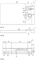
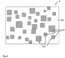
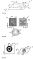
- Fig. 1a and Fig. 1b show a top view and a sectional view of a security document 1, which is provided with a decorative element 2.
- the Security Document 1 is the embodiment according to Fig. 1a and Fig. 1b a banknote.
- the security document 1 is any other security document, for example an ID document such as an identity card, a passport or a company ID, a credit card or debit card, a software certificate, a
- the security document 1 has a carrier substrate 10 to which the decorative element 2 is applied.
- the carrier substrate 10 preferably consists of a paper substrate.
- the carrier substrate 10 may consist of a plastic substrate or a multilayer substrate with one or more plastic and/or paper layers.
- security features such as watermarks or microperforations, to be incorporated into the carrier substrate 10, and for the carrier substrate 10 to be provided with further decorative elements, prints and the like, which provide further security features.
- the decorative element 2 has - as in Fig. 1a shown - has a strip-like shape and spans the entire width of the carrier substrate 10 from the upper longitudinal edge of the carrier substrate to the lower longitudinal edge of the carrier substrate.
- a transparent window 11 is also introduced into the carrier substrate 10, which is covered by the decorative element 2.
- the transparent window 11 can - as in Fig. 1b shown - in the form of a recess in the carrier substrate 10, which is introduced into the carrier substrate 10, for example, by means of a corresponding punching or a corresponding watermark.
- the transparent window 11 it is also possible for the transparent window 11 to be formed by a transparent region of the carrier substrate, in particular when the carrier substrate consists of a transparent plastic substrate.
- the decorative element 2 now has several areas in which an optical effect is generated by the decorative element 2 in incident light or transmitted light.
- areas 31 and 33 are shown, which are arranged in the area of the transparent window and which generate an optical effect when viewed through transmitted light.
- Fig. 1a Areas 32 and 34 are shown in which an optical effect is generated when viewed in incident light, ie in reflection.
- Areas 31 and 33 are further surrounded by a background area 35 in which the decorative element 2 has a transparent appearance, for example when viewed in transmitted light.
- Areas 32 and 34 are further surrounded by a background area 36 in which the decorative element 2 has an optical effect when reflected, for example a shiny metallic or matt or even colored appearance.
- the decorative element 2 has a microstructure in the areas 31, 32, 33 and 34, which generates an optical effect in incident light or transmitted light as described above.
- the microstructure has a special design in the areas 31 and 32 and comprises a base area and several base elements, each of which has an element surface that is raised and sunk relative to the base area and a flank arranged between the element surface and the base area.
- the exact design of the microstructure in the areas 31 and 32 is explained in detail below with reference to the figures. Fig. 1c to Fig. 16 explained.
- the microstructure is formed in the form of a diffraction grating, a hologram, a KINEGRAM ® , a microlens structure, a blaze grating, a macrostructure or another relief structure that differs from the formation of the microstructure in the areas 31 and 32, so that the decorative element 2 produces different optical effects, in particular different optically variable effects, in the areas 31 and 32 on the one hand and in the areas 33 and 34 on the other hand.
- the areas 32 and 34 and possibly also the areas 31 and 33 are arranged adjacent to one another and preferably form complementary and/or mosaic-like nested representations in order to further increase the security against forgery.
- the arrangement of the areas 31 and 33 in the area of the transparent window 11 as well as the arrangement of the areas 32 and 34 in the reflective area of the decorative element 2 is not limited to the Fig. 1a
- the arrangement shown is not limited to the number and arrangement of the areas 31 to 36, but both the number and the arrangement of the areas 31 to 36 can be arbitrary.
- the shape of the decorative element 2 can also differ from that shown in Fig. 1 a and Fig. 1b shown and have, for example, the shape of a patch or a security thread.
- the decorative element 2 does not have a transparent area that is designed for transmitted light viewing and thus only has the areas 34, 32 and 36.
- the decorative element 2 is only designed for transmitted light viewing and thus only has the areas 31, 33 and 35.
- the decorative element 2 is in the embodiment according to Fig. 1a and Fig. 1b as a laminating film.
- the decorative element 2 is designed as a transfer film, in particular as a hot stamping film, or as a security thread.
- the decorative element is provided by one or more layers of the security document.
- the decorative element 2 is not part of a security document and is designed, for example, in the form of a transfer film, a label or a sticker.
- Fig. 1c now shows a sectional view of a section of the decorative element 2, with the decorative element 2 being designed as a laminating film.
- the decorative element 2 has a carrier film 21, an adhesion-promoting layer 22, a plastic layer 23, a reflection layer 24, a plastic layer 25 and an adhesive layer 26.
- the carrier film 21 preferably consists of a transparent plastic film, for example a PET or BOPP film, with a layer thickness of between 20 ⁇ m and 250 ⁇ m.
- the surface of the carrier film can be provided with one or more functional layers, e.g. to improve printability.
- the plastic layer 23 preferably consists of a transparent plastic layer which has a transmissivity of more than 50%, preferably more than 80%, in the visible light range. It is also possible for the plastic layer 23 or the carrier film 21 to be colored with a dye. Coloring can change the color impressions and in particular also influences the formation of the complementary color impressions.
- the plastic layer 23 is preferably a lacquer layer which enables the molding of a relief structure into a surface of the plastic layer 23 by thermal replication or by means of UV replication.
- the plastic layer 23 is thus preferably a thermoplastic lacquer or a UV-curable lacquer.
- the reflection layer 24 is preferably an opaque reflection layer which preferably has a transmissivity of less than 50%, more preferably less than 20%, in the range of light visible to the human eye. These values refer to areas without a microstructure, i.e. mirror surfaces.
- the reflection layer 24 is preferably a reflection layer made of metal, in particular aluminum, silver, chrome or copper. It is also possible for the reflection layer 24 to consist of a high refractive index material (HRI), for example ZnS or TiO 2. When designed as a metal layer, the reflection layer 24 preferably has a thickness in the range of 10 nm to 100 nm and when designed from an HRI material, between 40 nm and 200 nm. The reflection layer 24 can be present over the entire surface or only partially.
- HRI high refractive index material
- the reflection layer 24 can consist of a multilayer system.
- the reflection layer 24 can thus consist, for example, of a sequence of high and low refractive materials or of a sequence of an absorption layer, a spacer layer and a reflection layer and thus be designed, for example, as a Fabry-Pérot filter.
- Such a multilayer system consists, for example, of a semi-transparent metal layer, a dielectric spacer layer and a mirror layer, for example an 8 nm chromium layer, a 400 nm SiO 2 layer or polymer layer and a 50 nm aluminum layer.
- the reflection layer 24 can be present over the entire surface or only partially.
- the plastic layer 25 preferably consists of a transparent polymer material and optionally has - as explained below - at least in the area of the areas 31 a refractive index which differs from the refractive index of the plastic layer 23 by at least 0.2. If no reflection layer 24 is provided, the plastic layer 25 can fulfill the function of a reflection layer.
- the plastic layers 23 and 25 preferably have a layer thickness between 1 ⁇ m and 8 ⁇ m.
- the adhesive layer 26 has a layer thickness of between 1 ⁇ m and 10 ⁇ m and serves to fix the decorative element 2 on the carrier substrate 10.
- the adhesive layer 26 preferably consists of a hot glue, a cold glue and/or a UV-curable glue. It is also possible for the adhesive layer 26 to be formed in two or more layers.
- the decorative element 2 is furthermore transparent in the area of the transparent window 11, so that all layers of the decorative element 2 provided in the area of the transparent window 11 are transparent.
- the adhesive layer 26 is preferably also transparent and clear, at least transparent and clear in the area of the transparent window 11.
- the decorative element 2 can be used in addition to the Fig. 1c shown layers may also have further decorative layers, adhesion-promoting layers, adhesive layers and carrier layers. Furthermore, it is also possible for the decorative element to consist only of layer 23 and, in particular, for the adhesion-promoting layer 22, the carrier film 21, the plastic layer 25 and/or the adhesive layer 26 to be dispensed with.
- the adhesion-promoting layer 22 and then the plastic layer 23 are first applied to the carrier film 21.
- a microstructure 4 is then molded into the plastic layer 23 using a replication tool, for example a replication roller.
- the microstructure 4 can be molded, for example, using heat and pressure when using a thermoplastic replication varnish for the plastic layer 23 or by means of subsequent UV irradiation when using a UV-curable replication varnish as the plastic layer 23.
- the reflective layer 24 is then applied, for example by vapor deposition or sputtering or printing.
- the reflective layer 24 is then optionally removed again in some areas, for example in the area of the transparent window 11. It is also possible to provide the reflection layer 24 only in a patterned form in the area 32, 33 and 36 and thus introduce an additional design element into the decorative element 2.
- the plastic layer 25 and then the adhesive layer 26 are then applied, for example by means of a printing process.
- the microstructure 4 is formed, for example, as a mirror surface in the areas 35 and 36 and as a diffractive structure 42 in the areas 33 and 34.
- the microstructure 4 has a base surface 40 and several basic elements 41, each of which has an element surface that is raised or sunk relative to the base surface and a flank arranged between the element surface and the base surface.
- the element surfaces of the base elements 41 each run essentially parallel to the base surface 40.
- the element surfaces of the base elements 41 and the base surface are spaced apart in a plane perpendicular to a base plane defined by the base surface 40 with a first distance which is selected such that a first color is generated in the regions 32 by interference of the light reflected on the base surface 40 and the element surfaces in the incident light in the first or a higher diffraction order or in the scattered light and/or that a first color is generated in the one or more first zones by interference of the light transferred through the element surfaces and the base surface 40 in the regions 31 in the transmitted light in the first or a higher diffraction order or in the scattered light.
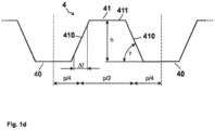
- Fig. 1d shows a section of the microstructure 4 in the area 31, 32.
- the microstructure 4 has the base area 40 and the base elements 41, each of which has an element surface 411 that is raised or recessed relative to the base surface 40 and a flank 410 arranged between the element surfaces 411 and the base surface 40.
- the element surfaces 411 of the base elements 41 run essentially parallel to the base plane.
- the element surface 411 adjacent to the respective flank 410 and the base surface 40 adjacent to it are spaced apart from one another at a step height h in a direction perpendicular to the base plane.
- the flank 410 of the microstructure 4 is preferably defined as a surface whose height is at least 10% of the step height h higher than the adjacent base surface 40 and at least 10% of the step height h lower than that of the adjacent element surface 411.
- the area portion of the flank projected onto the base plane is 100 % • 2 • ⁇ ⁇ p
- This area share of the flanks 410 is preferably less than 50%, more preferably less than 40%, even more preferably less than 30% and particularly preferably less than 20%. It has been shown that an increase in the area share of the flanks 410 leads to a reduction in efficiency and that the colors also become more pastel-like, i.e. more impure or white.
- the average flank angle ⁇ must meet the following condition: ⁇ ⁇ a r c t a n h 100 % ⁇ 2 • 10 % • X % • p
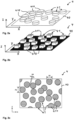
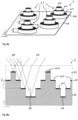
- the microstructure 4 has in the areas 31 and 32 or in a partial area of the areas 31 and 32, for example, the structures shown in the schematic three-dimensional representations of Fig. 2a and Fig. 2b
- the microstructure 4 here has the base area 40, which, as shown in the figures Fig. 2a and Fig. 2b indicated, a base plane spanned by the coordinate axes x and y is defined.
- the base elements 41 have element surfaces 411, which, as shown in the figures Fig. 2a and Fig. 2b shown, are arranged raised relative to the base surface 40.
- the microstructure 4 is not molded into the lower surface of the plastic layer 23, but into its upper surface, and thus the element surfaces 411 are not raised, but recessed relative to the base surface 40. Further flanks 410 are arranged between the element surfaces 411 and the base surface 40.
- the basic elements 41 thus each consist of an element surface 411 and a flank 410 enclosing it.
- the element surface 411 is spaced from a base plane defined perpendicularly from the coordinate axes x and y in the direction of a coordinate axis z with a specific distance which is selected such that a first color is generated in incident light or in transmitted light in the first or a higher diffraction order or in scattered light, as will be explained in detail later.
- the basic elements 41 are formed in the form of cylinders, which are arranged pseudo-randomly on the base plane. Furthermore, it is also possible for the basic elements 41 to have any other shape. Fig. 2b for example, a formation of the basic elements 41 in the form of cuboids.
- the element surfaces 411 are, as shown in the figures Fig. 2a and Fig. 2b shown, preferably arranged parallel to the base surface 40. However, it is also possible for the element surfaces 411 to be arranged only essentially parallel to the base surface 40 and thus, for example, the element surfaces 411 are slightly tilted relative to the base surface 40. It has proven advantageous here that tilting the element surfaces 411 relative to the base surface 40 in the range between 5 degrees and 30 degrees, preferably in the range from 5 degrees to 15 degrees, enables an increase in the scattering angle range and the color spectrum. In this context, "essentially parallel” is also to be understood as such tilting of the element surfaces 411 relative to the base surface 410.
- the surface coverage of the area or sub-area with the basic elements is between 30% and 70%, more preferably between 40% and 60%, and more preferably preferably around 50% or 1/2. This applies to two-stage microstructures. For three-stage microstructures, the surface coverage is preferably around 2/3, for four-stage microstructures around 3/4, etc.
- the flank angle of the flanks 410 is preferably greater than 70 degrees, more preferably greater than 80 degrees, and more preferably preferably approximately 90 degrees, as in the embodiments according to the following embodiments shown.
- Fig. 2c now shows an embodiment in which the basic elements 41 are arranged pseudo-randomly in the areas 31 and 32 or in a sub-area of the areas 31 and 32.
- the microstructure 4 is thus composed of one or more basic elements, whereby the arrangement of the basic elements in the x/y plane is pseudo-random.
- This pseudo-random arrangement suppresses or reduces undesirable diffractive effects, since there are no longer any periodic structures like in a grating.
- Fig. 2c now shows a plan view in a direction perpendicular to the base plane, ie in the direction of the z-coordinate axis, of a section of such a region of the microstructure 4 with several basic elements 41 and the base area 40.
- Fig. 2c now shows an embodiment in which the basic elements 41 are arranged pseudo-randomly in the areas 31 and 32 or in a sub-area of the areas 31 and 32.
- the microstructure 4 is thus composed of one or more basic elements, whereby the arrangement of the basic elements in
- the lateral extensions ⁇ x and ⁇ y of the basic elements in the x-/y-plane are in the range from 0.25 ⁇ m to 50 ⁇ m, preferably between 0.4 ⁇ m and 20 ⁇ m and more preferably between 0.75 ⁇ m and 10 ⁇ m.
- the term "lateral extension of the basic elements" is to be understood here as the lateral extension of the projection of the basic elements in a direction perpendicular to the basic plane.
- the minimum distance between adjacent basic elements ⁇ s is in the embodiment according to Fig. 2c pseudo-randomly selected. Preferably, the minimum distance between adjacent basic elements ⁇ s cannot take on all possible values, but only values from a narrower, predefined range of variation.
- the arrangement of the basic elements 41 is restricted in such a way that the basic elements 41 do not overlap and at the same time the minimum distance ⁇ s is not greater than 300 ⁇ m, preferably not greater than 50 ⁇ m. If overlapping basic elements are permitted, they are preferably manufactured in such a way that the plane at the overlap area has the same height as non-overlapping areas of the basic elements.
- the minimum distance ⁇ s between two adjacent basic elements is between 0.5 ⁇ m and 50 ⁇ m, more preferably between 0.5 ⁇ m and 20 ⁇ m.
- such a pseudo-random arrangement of the basic elements 41 is achieved by providing a two-dimensional grid spanned by the x and y axes in the corresponding area or sub-area, which defines a control position of the respective basic element 41 in the base plane.
- the basic elements are then positioned in this area or in this sub-area by a pseudo-random shift from the respective control position in the direction of the coordinate axes x and/or y, wherein the range of variation of this pseudo-random shift is selected such that the conditions set out above for the minimum spacing of two adjacent basic elements 41 are preferably met.
- the minimum distance between two adjacent basic elements is determined pseudo-randomly and then, starting from these two basic elements, the minimum distance of the basic elements adjacent to these basic elements is selected pseudo-randomly, etc. and in this way a corresponding pseudo-random positioning of the basic elements 41 is achieved.
- the pseudo-random variation for example the pseudo-random shift of the basic elements from the control position or the pseudo-random variation of the minimum distance between the basic elements, can take all values from the narrower, predefined variation range into account with equal probability.
- a mathematical function for the probability of taking a value from this variation range into account examples of such functions are the Gaussian function and an inverted Gaussian function.
- the predefined variation range to include several predefined values from which a value is selected pseudo-randomly. For example, it is possible to select the minimum spacing ⁇ s between two basic elements 41 from a variation range which, for example, includes 10 values in increments of 0.5 ⁇ m.
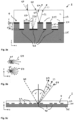
- Fig. 3a now shows a schematic sectional view of the decorative element 2 in the area of the microstructure 4 according to Fig. 2c .
- the decorative element 2 here has the plastic layers 23 and 25 and the reflective layer 24.
- the plastic layer 23 has a refractive index n 1 and the plastic layer 25 has a refractive index n 2.
- the microstructure 4 has the base area 40 and several base elements 41 with the element surfaces 411 and the flanks 410.
- the microstructure 4 is coated with the reflective layer 24, which has a thickness d, and is further embedded in the plastic layers 23 and 25.
- the flank angle of the flanks 410 is greater than 70 degrees, in particular greater than 80 degrees and preferably almost vertical (almost 90 degrees).
- the lower surfaces of the reflection layer 24 in the region of the element surfaces 411 and in the region of the base surface 40 are spaced apart from one another in the direction of the z-axis by a height h, so that the first distance, ie the spacing 61 of the element surfaces 411 from the base surface 40, also has the value h.
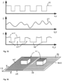
- the light 50 incident from the air onto the decorative element 2 at an angle of incidence ⁇ * is refracted by the plastic layer 23 and thus, taking into account the refraction of light, strikes the basic elements 41 and the base surface 40 of the microstructure 4 at the angle ⁇ .
- the law of refraction of sin ⁇ ⁇ n 1 ⁇ sin ⁇
- the light 50 incident on the microstructure interacts with the microstructure 4 in two ways. Firstly, the incident light 50 is reflected due to reflection at the reflection layer 24 in the planes determined by the element surfaces 411 and the base surface 40, which are spaced apart by the distance 61 and thus the value h.
- the law of reflection of angle of incidence angle of departure applies here.
- the height h is preferably in the range from 150 nm to 1000 nm, particularly preferably between 200 nm and 600 nm.
- the microstructure 4 in the region 31 or in a partial region of the region 31 generates a colour in the zeroth diffraction order by means of interference when viewed through transmitted light in transmission.
- the reflection layer 24 may not be provided in this area, so that the microstructure 4 is embedded directly between the plastic layers 23 and 25.
- a transparent high-refractive reflection layer 24 is used.
- light scattering also occurs due to the lateral extent, for example the lateral extent ⁇ x of the basic elements, as described above. Due to the lateral extent of the basic elements chosen as described above parallel to the ground plane, scattered radiation occurs. Structures of the size of the basic elements 41 scatter light more in the forward direction. The light scattered by the irregularly arranged basic elements 41 is distributed in a solid angle range around the directly reflected or directly transmitted light rays, i.e. around the zeroth diffraction order. The lateral extent of the basic elements determines the angular range around which light scattered around the zeroth diffraction order is generated by the microstructure. The larger the lateral extent of the basic elements 41, the more pronounced the forward scattering. Consequently, the scattering angle ⁇ , which encompasses the angular range in which the microstructure deflects the light by scattering from the zeroth diffraction order, becomes smaller the larger the fundamental elements 41 are.
- Fig. 3b and Fig. 3c illustrate this effect.
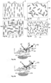
- Fig. 3b shows a plan view of two basic elements 41, which illustrates different degrees of forward scattering of two exemplary basic elements 41 of different sizes.
- Fig. 3c shows a corresponding sectional view of the decorative element 2 with the plastic layers 23 and 25 as well as the reflection layer 24 and the microstructure 4 with the basic elements 41 and the base area 40.
- the light 50 incident at the angle ⁇ * is reflected directly by the decorative element in the zeroth diffraction order and thus generates the light 53.
- the microstructure 4 generates scattered light 54 in an angular range ⁇ around the light 53 reflected in the zeroth diffraction order.
- a corresponding generation of scattered light is also effected in an analogous manner in a microstructure 4 designed for transmitted light observation, so that reference is also made here to the above explanations.
- Isotropically formed basic elements 41 such as those in Fig. 2a and 2c shown basic elements generate scattered light 54 up to the scattering angle ⁇ .
- the scattering angle ⁇ is given by the minimum length of the projection of the basic element 41 used onto the base plane and thus by the corresponding lateral dimension of the basic element 41, for example determined by the diameter of the circle in the case of a circular disk-shaped projection of the basic element onto the base plane.
- ⁇ is in the range of +/- 30 degrees and more preferably +/- 15 degrees.
- the scattered light 54 usually has the complementary color impression compared to the light beam 53, which can be observed in the zeroth diffraction order. Due to the conservation of energy, in this case the incident white light must be split into the directly reflective light 53 and the scattered light 54, which leads to the complementary color impression.
- the incident light 50 which does not undergo constructive direct reflection or transmission and is not absorbed, is mostly found in the scattered light. If the scattered light appears greenish, for example, the light reflected directly in the zeroth diffraction order appears violet.
- the complementary color impression arises above all when the reflection layer 24 consists of a color-neutrally reflective material such as aluminum or silver.
- aluminum reflects light across the entire visible spectral range with approximately 90% efficiency and is therefore suitable for creating complementary color impressions.
- Copper on the other hand, has a stronger absorption in the short-wave, i.e. blue, spectral range and changes the color impressions accordingly because copper does not reflect color-neutrally.
- the size of the basic elements can also be varied pseudo-randomly.
- Fig. 4 shows, for example, a top view of the microstructure 4 with the base area 40, the basic elements 41 and the element surfaces 411.
- the element surfaces 411 of the basic elements 41 have a square shape, wherein the size of the squares varies from basic element 41 to basic element 41 within a predetermined range of variation.
- the dimension of the projection of the respective basic element onto the base plane in the direction of the x-axis and/or y-axis is preferably varied pseudo-randomly within a predetermined range of variation.
- the spacing of the basic elements from the next neighboring basic element it is also possible to vary the shape of the projection of the basic element onto the ground plane or the lateral preferred direction of the projection of the basic element onto the ground planes pseudo-randomly within a predefined range of variation. It is also possible that only one of the parameters listed above is varied pseudo-randomly within a predefined range of variation.
- basic elements 41 were described which form symmetrical basic elements in the sense that their projection onto the base plane in a direction perpendicular to the base plane has a symmetrical surface shape.
- the use of asymmetrical basic elements is particularly advantageous in which the projection of the respective basic element onto the base plane has an asymmetrical shape with a lateral dimension in a preferred direction in the base plane which is larger than the lateral dimension of the projection transverse to the preferred direction, preferably 50% larger, preferably more than 80% larger, more preferably more than 2 times and in particular more than 5 times larger than the dimension transverse to the preferred direction.
- Complex optical effects can be achieved with such asymmetrical basic elements.
- the colour impression of the scattered light changes when the security element is rotated in the x/y plane, i.e. when it is rotated around the z-axis and the viewing angle is maintained.
- the scattered light can appear cyan or light blue or turquoise when viewed in the x/z plane and When rotated in the y/z plane, it changes to dark blue/green or dark grey. The effect appears as an anisotropic matte colour.
- Fig. 5b shows the formation of the microstructure 4 in an area 313 of the decorative element 2.
- the microstructure 4 here has a large number of basic elements 41 and the base area 40.
- the basic elements 41 are also formed as asymmetrical basic elements.
- the basic elements 41 are not only positioned pseudo-randomly in the base plane, but their preferred direction 418 is also pseudo-randomly varied within a predefined range of variation from basic element to basic element.
- the scattering angle range is larger compared to symmetrical basic elements.
- the pseudo-random variation of the preferred direction of the basic elements 41 can cover the entire angular range from minus 180 degrees to plus 180 degrees.
- the angular range can also be restricted, however, and as already stated above, preferably between minus 90 degrees and plus 90 degrees, more preferably minus 30 degrees and plus 30 degrees.
- Fig. 5c shows a further embodiment of the formation of the microstructure 4 in the areas 31 and 32 of the decorative element 2.
- FIG. 5d shows an embodiment of such a configuration of a region of the microstructure 4 of the decorative element 2 with a first cell 314 and a third cell 316, in which the basic elements 41 are designed as symmetrical basic elements.
- the size of the cells is preferably more than 300 ⁇ m, more preferably more than 500 ⁇ m, more preferably more than 1 mm and in particular more than 5 mm.
- movement effects are generated when rotating, e.g. "rolling bar"-like effects are generated.
- the size of the first, second and third cells 314 to 316 is selected to be below the resolution limit of the human eye, preferably smaller than 300 ⁇ m and more preferably smaller than 100 ⁇ m. With such a shape of the cells 314 to 316, the color impression of the scattered light is a mixture of the effects of the individual cells 314 to 316.
- the decorative element contains a hidden security element. When viewed under a microscope, the brightness of the various cells differs if the resolution is selected to be high enough.
- Fig. 7 have the shapes shown as examples, and thus, for example, have the shape of a circular disk, a square, an ellipse, a rectangle, a hexagon, a currency symbol, a denomination symbol, a letter, the shape of a symbol, for example a heart shape, a cross, a ring, a circle with nanotext or a star.
- the basic elements or their projection onto the basic planes can also be formed by letters and symbols which form a microtext due to the arrangement of the basic elements on the basic plane.
- the basic elements which form the microtext have a pseudo-random variation in the positioning of the basic elements in the first area or in at least a first partial area of the first area, wherein the microtext is readable despite the variation.
- the shape of the basic elements or The shape of the projection of the basic elements onto the base plane can in this way also provide a hidden security feature in the decorative element 2.
- the decorative element for example using optical microscope technology, the shape of the basic elements or the shape of the projection of the basic elements onto the base plane can be verified and the hidden security feature can thus be checked.
- the arrangement of a shape of the basic elements can also carry hidden information. For example, if the microstructure is made up of 95% basic elements of one shape - e.g. circles - and 5% basic elements of another shape - e.g. crosses - the arrangement of the crosses can be the hidden information.
- the basic elements 41 it is also possible for the basic elements 41 to have not only one element surface, but also several element surfaces, which influence the interference of the incident light and thus the generation of the color. Such an embodiment is described below by way of example with reference to the figures Fig. 8a and Fig. 8b described.
- Fig. 8a shows a three-dimensional representation of the section of the microstructure 4 in one of the areas 31 and 32.
- the microstructure 4 here has the base area 40 and a plurality of basic elements 41, of which Fig. 8a four pieces are shown.
- the basic elements 41 not only have the element surface 411, but also further element surfaces 412 and 413. These element surfaces 412 and 413 are also arranged essentially parallel to the base surface 40 and further in the direction of the z-axis from the base surface when the basic elements 41 are arranged in one of the first zones with a multiple of the first distance, i.e. the distance 61.
- the element surfaces 412 and 413 are thus also spaced from each other and from the element surface 411 by the distance h, so that the interference condition, as previously described using Fig. 3a explained, is also fulfilled for the element surfaces 412 and 413.
- the area of the element surfaces 411, 412 and 413 is as equal as possible. This means that the area share of each step including the base area is approximately the same size, e.g. in the case of four-step basic elements, approximately 1/4.
- Fig. 8b shows a corresponding sectional view of a section of the decorative element 2 with the plastic layers 23 and the reflection layer 24.
- the light 50 incident at the angle ⁇ is reflected here in the zeroth diffraction order as light 53, whereby the light rays reflected at the base surface 40, at the element surfaces 411, at the element surfaces 412 and at the element surfaces 413 overlap and a color is generated by constructive or destructive interference from the microstructure 4.
- the base elements 41 can be designed not only in three stages, but also in two stages or in multiple stages and thus have one or more further element surfaces in addition to the element surface 411, which are preferably arranged as previously explained.
- the color purity when viewed in the zeroth diffraction order is significantly increased by introducing these additional planes. It is preferred that the surface areas of the various element surfaces on the projection of the basic element 41 on the basic plane are the same, which also results in the purest colors.
- the height h at which the additional element surfaces 412 and 413 are spaced apart is preferably the same.
- the height h is preferably in the range from 150 nm to 1000 nm and particularly preferably in the range from 200 nm to 600 nm.
- the multi-level design has the advantage of better directed constructive interference and thus a stronger color impression.
- the greater the number of element surfaces spaced apart from one another the narrower the spectrum of the constructively reflected light.
- the number of element surfaces of the basic elements spaced apart from one another is preferably selected in the range from 2 to 6.
- the projection of the basic elements 41 can thus have the shape shown in the figures Fig. 7 , Fig. 5a to Fig. 5d , Fig. 4 and Fig. 2a to Fig. 2c shown shape.
- the further element surfaces and the element surface 411 are further formed in such a way that they result in a concentric, pyramid-shaped structure and thus the element surfaces 411 and 412 have a band-shaped shape that follows the outer contour.
- the surface area of the element surfaces is the same.
- the microstructure in the regions 31 and 32 or in one or more sub-regions of the regions 31 and 32 has a periodic arrangement of basic elements 41, the projection of which onto the base plane preferably has an identical shape.
- the projection of the basic elements onto the base plane preferably has the form of webs or points.
- the basic elements preferably follow one another periodically isotropically or pseudo-isotropically in the direction of an azimuth angle, which thus describes the spatial direction of the sequence in the x/y plane.
- the distance of the element surfaces of the basic elements from the base surface is preferably constant.
- Fig. 9a shows a plan view of a partial area of the microstructure 4 forming a cell 320.
- the cell 320 comprises several partial areas 321 in which the basic elements 41 each follow one another periodically. This is shown by way of example in Fig. 9b explained.
- the microstructure 4 has the base surface 40 and the base elements 41 with the element surfaces 411 and the flanks 410.
- the base elements 41 are designed in the form of webs, the cross section of which is shown in the lower illustration of Fig. 9b and whose extension in the x/y plane in the figures Fig. 9a and Fig. 9b is indicated by a corresponding line.
- the cross section of the basic elements 41 of the respective sub-area 321 is identical and the projection of the basic elements 41 onto the ground plane follows, as shown in the figures Fig. 9a and Fig. 9b indicated, periodically in the direction of a respective azimuth angle 419.
- the microstructure 4 is thus in the partial areas 321 each by the parameter azimuth angle 419 by the basic element shape, for example the web-shaped shape according to the lower illustration according to Fig. 9b , and by the spatial frequency and thus the period in which the basic elements 41 follow one another in the direction of the azimuth angle 419.
- one or more of the parameters azimuth angle, basic element shape and/or spatial frequency of the sub-areas 321 arranged in the cell 320 are varied pseudo-randomly from sub-area 321 to sub-area 321 within a variation range predefined for the cell 320.
- the cell 320 shown has sub-areas 321 in which the azimuth angle 419 and thus the orientation of the basic elements 41 in the various sub-areas 321 is pseudo-randomly varied.
- the azimuth angle varies pseudo-randomly and thus isotropically between 0 and 180 degrees in 15 degree increments.
- the distance between the element surfaces of the basic elements 41 in the sub-areas 321 is preferably constant, but can also be varied pseudo-randomly.
- the pseudo-random orientation of the azimuth angle 419 can cover the entire angle range from minus 180 degrees to plus 180 degrees. However, it is also advantageous to limit the angle range and thus the range of variation of the pseudo-random variation. It is further preferred to vary the azimuth angle 419 between minus 90 degrees and plus 90 degrees, more preferably between minus 30 degrees and plus 30 degrees.
- microstructure 4 in the regions 31 and 32 or in partial regions of the regions 31 and 32 in the form of a circular grid, in which the basic elements 41 preferably have a circular ring-shaped shape.
- the period in which the basic elements 41 periodically follow one another is preferably in the range from 0.75 ⁇ m to 10 ⁇ m for the microstructures explained above.
- the size of the sub-areas 321 is preferably in the range from 5 ⁇ m to 100 ⁇ m and more preferably between 10 ⁇ m and 30 ⁇ m.
- the size of the cells 320 is preferably selected between 40 ⁇ m and 300 ⁇ m, more preferably between 80 ⁇ m and 200 ⁇ m.
- the basic elements can be made in accordance with the embodiments according to Fig. 8a and Fig. 8b be designed in several stages with several element surfaces.
- the several stages can be symmetrical - ie like a staircase that ascends and then descends again - or asymmetrical - ie like a staircase that only ascends or only descends.
- the distance of the element surfaces 411 from the base surface 40 is in the range from 150 nm to 2000 nm, more preferably in the range from 200 nm to 1000 nm and more preferably in the range from 200 nm to 500 nm.
- the complementary color impression is not reflected in scattered light, but in the diffraction in the first and partially higher order.
- the diffraction does not appear as a rainbow color effect or at least only greatly attenuated. Due to the energy retention, a large part of the light that is not constructively deflected in the zeroth diffraction order goes into the first or higher diffraction order, so that the color impression when viewed at least outside the zeroth diffraction order is largely determined by the complementary color impression of the color when viewed in the zeroth diffraction order.
- the period and shape of the basic elements 41 should be selected here such that a large part of the light deflected from the zeroth diffraction order is deflected in an angular range ⁇ of +/- 30 degrees around the zeroth diffraction order in order to achieve the advantageous optical effect explained above.
- the basic elements 41 of the microstructure 4 are positioned in the regions 31 and 32 or in a partial region of the regions 31 and 32 following a non-periodic function.
- Fig. 10 shows an example of a plan view of an area 322 of the decorative element 2, which Fig. 10a The optical information shown is generated by means of such an arrangement of the basic elements.
- Fig. 10b shows an associated spectrum of a first color impression and the associated color diagram.
- the basic elements are arranged with a distance 61 of the element surfaces 411 and the base surface 40 of 330 nm and the arrangement of the basic elements on the base plane and the shape of the projection of the basic elements on the base plane are as shown below with reference to the figures Fig. 11a to Fig. 11d
- the shape of a three-dimensional object for example the one shown in the illustration according to Fig. 10a shown key.
- the representation of the three-dimensional object appears bluish.
- the three-dimensional object appears yellow.
- the decorative element is tilted, the blue and yellow areas change accordingly, so that a three-dimensional impression of the three-dimensional object is visualized by the decorative element.
- Fig. 11a now shows a plan view of a section of the area 322, when viewed perpendicular to the plane spanned by the base plane.
- Fig. 11b shows a corresponding sectional view of the decorative element 2 in a partial area of the area 322 along the line AA' from Fig. 11a .
- the decorative element 2 has the plastic layers 23 and 25 as well as the reflection layer 24. Furthermore, the microstructure 4 is provided, which in the partial area 322 has the base surface 40 and the base elements 41, whose element surfaces 411 are spaced from the base surface 40 at a distance 61 in the direction of the z-axis.
- the base elements 41 are here - as in the figures Fig. 11a and Fig. 11b shown - are generally not arranged in a periodic sequence and also differ in the shape and size of the projections onto the base plane.
- the arrangement of the basic elements 41 and the surface dimensions of the projections of the respective basic elements 41 in the area 322 are determined by a function which describes a binary diffraction structure which deflects the incident light according to a predefined three-dimensional free-form surface with one or more free-form elements.
- a free-form element can be formed, for example, from a section of a surface of a three-dimensional object, as is shown, for example, in the illustration according to Fig. 10 has taken place.
- the free-form element is formed from a section of the surface of a three-dimensional object, namely a key. It is also possible that free-form elements are free-form elements in the form of an alphanumeric character, a geometric figure or another object that produce magnification, reduction and/or distortion effects.
- the binary diffraction structure can be created, for example, by means of a lithographic mask process or by means of a lithographic direct writing process (e.g. Ebeam or laser writer).
- a lithographic direct writing process e.g. Ebeam or laser writer.
- the projections of the basic elements or the element surfaces of the basic elements are thus selected depending on the local curvature of the three-dimensional object, whereby in the area of strong curvature the spacing of the basic elements and the surface dimensions of the projections or the element surfaces are reduced across the curvature.
- Fig. 11a and Fig. 11b show an example of a section of such an arrangement of the basic elements.
- the basic elements 41 in the area of the curvatures of the free-form surfaces, which mainly contribute to the color impression, have a lateral extension in the x/y plane in at least one direction in the range of 0.25 ⁇ m to 500 ⁇ m, preferably between 4 ⁇ m and 100 ⁇ m.
- the width of the basic elements 41 in the area shown in Fig. 11a shown section and the spacing of the basic elements along the section line AA' are dimensions from the aforementioned range.
- the variation in the width of the basic elements 41 and the spaces between the basic elements 41 here follows a function f (x, y) which reflects the shape of the freeform surface and - as explained above - the change in the elevation of the freeform surface in relation to the z-axis.
- the distance 61 of the element surfaces 41 from the base surface 40 is selected as explained above. Surprisingly, it has been shown on the basis of practically manufactured prototypes that the significantly larger selection of the structure depth 61 in accordance with the principles discussed above only changes the optical effect of a three-dimensional freeform surface insignificantly and generates additional color information.
- the first or higher diffraction order receives a color modulation which appears as a clear non-rainbow color, in combination with the unchanged effect of a three-dimensional freeform surface.
- the first diffraction order usually has a complementary
- the perceptibility of the key shown in area 322 is essentially determined by the first-order diffracted and color-changed portions of the reflected light, which appears bluish, and the zero-order reflected light, which appears yellowish, is less perceptually noticeable.
- a microstructure according to Fig. 11c shows no pronounced dependence of the diffraction efficiency on the wavelength in the visible spectral range and thus a known rainbow colour effect when viewed with the human eye.
- Such a microstructure shows practically no memorable colour effect in the sense of the invention, which only occurs when the diffraction efficiency is clearly dependent on the wavelength, as for example in Fig. 11d shown.
- a hologram of one or more virtual 2D and/or 3D objects is calculated and ideally both the amplitude and the phase of the hologram are calculated and the hologram is binarized.
- a binary computer-generated hologram for example a kinoform, is used as a function.
- Fig. 12a shows the binarization based on a possible phase progression 600 of a computer-generated hologram. Shown is a schematic representation of a section with height in the z-direction as a function of the position in the x/y-direction.
- the phase value above a limit value 60 which is indicated by a dashed line, is set to a maximum value of the height and below it to a minimum value of the height. As in the lower illustration of Fig. 12a shown, this results in a binary function.
- the difference between the maximum value of the height and the minimum value of the height is now selected according to the distance 61 determined as previously and thus determines the color impression of the corresponding area of the decorative element 2.
- the optimal laser wavelength for reconstructing the hologram is twice the step height times the refractive index of the surrounding medium, with the distance 61 selected here as the step height.
- the area coverage is determined by the hologram information and the binarization algorithm.
- FIG. 12b and 12c An example of a computer-generated binary hologram is shown schematically in Fig. 12b and 12c shown.
- the template 601 is shown, which is used to calculate the hologram. In this case, this is the letter "K".
- the desired target image 602 is shown based on this template 601, which is calculated as a hologram.
- the K floats behind the hologram plane, with the right edge of the K being closer to the hologram plane than the left edge. This is indicated by the shadow.
- the reconstruction 603 of the binarization of the calculated computer-generated hologram is shown.
- Fig. 12c shows schematically the respective section 611, 612 and 613, ie a section in the x/z plane.
- the K 614 is in the hologram plane.
- the K 614 is shown behind the hologram plane 615.
- the section 613 of the reconstruction of the hologram is shown by the binary computer-generated hologram. Since the hologram is binary, not only the target image, i.e. the K 614 behind the hologram plane 615, is created, but also the mirror image 614', which appears to float in front of the hologram plane 615.
- the basic elements 41 of the microstructures in the areas 31 and 32 do not have a uniform spacing of the element surfaces from the base surface.
- the microstructure in the regions 31 also has one or more second and/or third zones in which the element surfaces are spaced apart from the base surface 40 in the direction of the coordinate axis z by a second or third distance or a multiple of a second or third distance which is different from the first distance.
- the second and third distances are selected such that interference of the light reflected from the base surface 40 and the element surfaces 411 in incident light in the first diffraction order or in scattered light and/or interference of the light transmitted through the element surfaces 411 and the base surfaces 40 in transmitted light in the first or higher diffraction order or in scattered light generates a third or fourth color in the one or more second or third zones which is different from the first color.
- microstructure 4 consists of a mixture of basic elements 41 with different distances 61 and 62, a corresponding color impression results, which is formed from a mixture of the individual color impressions.
- the following color effect can be achieved by rotating the decorative element 2 about an axis perpendicular to the base plane: If, for example, the basic elements 41 with the distance 61 for a certain viewing angle ⁇ * and when viewed parallel to the longitudinal axis of the basic element (i.e. in the y direction) produce a clearly visible, reddish color impression in scattered light, when rotated by 90 degrees (maintaining the viewing angle ⁇ *) a (only weakly visible) reddish or no color impression and the basic elements 42 with the distance of the element surfaces from the base surface 62 for this viewing angle ⁇ * and when viewed parallel to the longitudinal axis of the basic elements (i.e.
- a microstructure is provided in the areas 31 and 32 or in a sub-area of the areas 31 and 32, which uses basic elements 41 with different spacings 61 and 62, wherein the basic elements are not mixed, but are present in at least two macroscopic areas.
- the lateral size of these areas is typically larger than 300 ⁇ m and smaller than 50 mm.
- the macroscopic areas can be designed in the form of logos, characters or the like.
- Fig. 13c now illustrates an embodiment of this embodiment, whereby first zones 333 are provided in which basic elements 41 are provided with a distance 61 of the element surfaces from the base surface and several second zones 334 in which basic elements 41 are provided with a distance 62 of the element surfaces from the base surface.
- first zones 333 are provided in which basic elements 41 are provided with a distance 61 of the element surfaces from the base surface and several second zones 334 in which basic elements 41 are provided with a distance 62 of the element surfaces from the base surface.
- one zone is color-constant when rotated, while the other zone varies in the brightness of the color and thus, for example, the zones 334 arranged in the background vary in the brightness of their color.
- zones 333 and 334 the area coverage of the base plane with the basic elements is varied in order to vary the color brightness of the respective zone to generate a grayscale image. If the area coverage of a respective sub-area of zones 333 and 334 with the basic elements is close to 50%, the greatest brightness of the color results, and if the area coverage of the respective sub-area is reduced or increased, the brightness of the color decreases.
- the color value of the color is determined by the distance between the element surfaces of the basic elements of the base plane, i.e. by the distances 61 and 62 of the basic elements 41.
- additional information is encoded in zones 334 or 333 in this way, so that zone 334 also has a portrait of a person visible in grayscale representation as additional information.
- the brightness of this grayscale image can also be varied by overlaying it with other grid structures. It is particularly advantageous to provide moth-eye structures. These structures are preferably provided by cross grids or hexagonal grids with a period in the range of 200 nm to 400 nm and a grid depth/period ratio of between 0.5 and 2. By using such moth-eye structures, partial areas of zones 333 and 334 can be made darker and a grayscale image can be generated in this way.
- Fig. 14a shows, for example, a true color image 70.
- the image area of the true color image 70 is now divided into a plurality of pixel areas and the color value and the color brightness in the respective pixel area are determined.
- An image area of the decorative element 2 is then divided into a plurality of pixel areas and first, second and/or third zones are arranged in each of the pixel areas such that the color and color brightness values determined for the respective pixel area are generated by the microstructure 4.
- Fig. 14b shows, for example, a section of such an image area with four pixel areas 350.
- zones 351, 352 and 353 are provided in the pixel areas 350.
- the basic elements arranged in the zones 351, 352 and 353 have a different distance of the element surfaces from the base surface, namely the distance 61, 62 and 63, as can also be seen in the sectional view according to Fig. 14c
- the cut is shown in Fig. 14b marked with BB'.
- the shape and arrangement of the basic elements 41 in the respective zones 351, 352 and 353 is preferably in accordance with the preceding statements according to Fig. 2a to Fig. 12 chosen.
- a microstructure 80 is first formed in accordance with the above explanations and then, in a second step, the element surfaces and/or the base surface of the microstructure are slightly modulated by exposing a hologram 81 or writing a computer-generated hologram. This locally changes the height of the element surfaces or base surface slightly. This does indeed disturb the interference and thus changes the color of the microstructure 4, as can be seen in the lower illustration of Fig. 15 is shown, which is why the modulation must also be low.
- the image information of the hologram is stored in the microstructure 80, which, however, is accompanied by strong noise due to the low (light) modulation.
- the strength of the modulation can be in the range of +/- 50% of the height, but is preferably in the range of +/- 20% and more preferably in the range of +/- 10%. If only the element surface or the base surface is modulated, the color effects of the microstructure are more pronounced and therefore visible. However, as mentioned above, the image information of the hologram is very noisy. If both levels are modulated, the disturbance of the color effects is greater. The image information of the hologram is not very noisy. When viewed in ambient light, the hidden information is not or almost barely visible (due to the very low modulation). When illuminated with suitable laser light, the hologram appears.
- FIG. 16 Another, in Fig. 16 The embodiment shown provides for a modulation of the element surface of the basic elements 41 and/or the base surface 40 with a special grating structure.
- a diffractive structure 82 in a region 361 the base surface and the element surface of the basic elements 41 are modulated with a diffractive structure 82 and in a region 362 the base surface 40 and the element surfaces of the basic elements 41 are modulated with a diffractive structure 83.
- the diffractive structures 82 and 83 differ in the orientation of their grating lines, as shown in Fig. 16 is indicated.
- the grating structures can be linear, crossed or hexagonal.
- the grating period of the gratings 82 and 83 is preferably selected between 100 nm and 2000 nm, more preferably between 200 nm and 500 nm.
- the gratings 82 and 83 can be part of a design.
- the gratings 82 and 83 can be zero-order polarization gratings. This allows areas to be provided with a logo or background which is TE-polarized and other areas, e.g. the background of the logo or image, with the orthogonal polarization TM.
- TE-polarized light is understood to mean that in which the electric field component is parallel to the grating lines and TM-polarized light is understood to mean that in which the electric field component is perpendicular to the grating lines.
- the logo or image appears when viewed with a polarizing filter. Accordingly, the areas 361 and 362 can be designed as a background and pattern area, which are only visible when viewed through a polarizer.
- the modulation of the grating structure must be low, in particular in the range of +/- 50% of the height, but preferably in the range of +/- 20% and more preferably in the range of +/- 10%.
- the modulation depth of the hologram or the diffraction grating is preferably less than 100 nm, particularly preferably less than 50 nm and more preferably less than 30 nm. As a result, the modulation only slightly disturbs the interference that creates the color effect.
- a further preferred embodiment combines the previously described microstructures generating color effects with refractive, achromatic micromirrors as used, for example, in DE 10 2008 046 128 A1 described.
- the ground plane is defined by the micromirrors, i.e. the ground plane changes from micromirror to micromirror.
- the depth of the microstructures on the micromirror i.e. the distance 61, is preferably the same so that the achromatic effect of the micromirrors is superimposed on the color effect of the microstructures.
- Fig. 17 shows this embodiment in a schematic side view.
- a different base plane is provided, which is defined by the micromirrors, in particular by the DE 10 2008 046 128 A1 formed micromirror.
- the element surfaces 411 of the basic elements and the base surfaces 40 are aligned parallel to the respective base plane.
- the base planes in the areas 61, 62 and 63 are not arranged parallel to each other, but are tilted against each other, as in Fig. 17 shown.
Landscapes
- Physics & Mathematics (AREA)
- General Physics & Mathematics (AREA)
- Optics & Photonics (AREA)
- Engineering & Computer Science (AREA)
- Computer Security & Cryptography (AREA)
- Diffracting Gratings Or Hologram Optical Elements (AREA)
- Credit Cards Or The Like (AREA)
- Laminated Bodies (AREA)
- Optical Filters (AREA)
- Holo Graphy (AREA)
Priority Applications (2)
| Application Number | Priority Date | Filing Date | Title |
|---|---|---|---|
| RS20181298A RS57820B1 (sr) | 2012-06-26 | 2013-06-25 | Dekorativni element kao i sigurnosni dokument sa dekorativnim elementom |
| EP18189465.0A EP3422056B2 (de) | 2012-06-26 | 2013-06-25 | Dekorelement sowie sicherheitsdokument mit einem dekorelement |
Applications Claiming Priority (2)
| Application Number | Priority Date | Filing Date | Title |
|---|---|---|---|
| DE102012105571.8A DE102012105571B4 (de) | 2012-06-26 | 2012-06-26 | Dekorelement sowie Sicherheitsdokument mit einem Dekorelement |
| PCT/EP2013/063195 WO2014001283A1 (de) | 2012-06-26 | 2013-06-25 | Dekorelement sowie sicherheitsdokument mit einem dekorelement |
Related Child Applications (2)
| Application Number | Title | Priority Date | Filing Date |
|---|---|---|---|
| EP18189465.0A Division EP3422056B2 (de) | 2012-06-26 | 2013-06-25 | Dekorelement sowie sicherheitsdokument mit einem dekorelement |
| EP18189465.0A Division-Into EP3422056B2 (de) | 2012-06-26 | 2013-06-25 | Dekorelement sowie sicherheitsdokument mit einem dekorelement |
Publications (3)
| Publication Number | Publication Date |
|---|---|
| EP2864130A1 EP2864130A1 (de) | 2015-04-29 |
| EP2864130B1 EP2864130B1 (de) | 2018-08-29 |
| EP2864130B2 true EP2864130B2 (de) | 2024-10-02 |
Family
ID=48699024
Family Applications (2)
| Application Number | Title | Priority Date | Filing Date |
|---|---|---|---|
| EP13731331.8A Active EP2864130B2 (de) | 2012-06-26 | 2013-06-25 | Dekorelement, sicherheitsdokument mit einem dekorelement sowie verfahren zur herstellung eines dekorelements |
| EP18189465.0A Active EP3422056B2 (de) | 2012-06-26 | 2013-06-25 | Dekorelement sowie sicherheitsdokument mit einem dekorelement |
Family Applications After (1)
| Application Number | Title | Priority Date | Filing Date |
|---|---|---|---|
| EP18189465.0A Active EP3422056B2 (de) | 2012-06-26 | 2013-06-25 | Dekorelement sowie sicherheitsdokument mit einem dekorelement |
Country Status (12)
| Country | Link |
|---|---|
| US (1) | US10007233B2 (enExample) |
| EP (2) | EP2864130B2 (enExample) |
| JP (1) | JP2016505161A (enExample) |
| CN (1) | CN104903117B (enExample) |
| AU (1) | AU2013283489B2 (enExample) |
| DE (1) | DE102012105571B4 (enExample) |
| ES (1) | ES2689050T5 (enExample) |
| FI (1) | FI2864130T4 (enExample) |
| HU (1) | HUE042141T2 (enExample) |
| PT (1) | PT2864130T (enExample) |
| RS (1) | RS57820B1 (enExample) |
| WO (1) | WO2014001283A1 (enExample) |
Families Citing this family (83)
| Publication number | Priority date | Publication date | Assignee | Title |
|---|---|---|---|---|
| EP3450196B2 (en) | 2014-03-27 | 2025-05-21 | Toppan Printing Co., Ltd. | Display body and observing method for display body |
| EP2927013A1 (en) * | 2014-03-31 | 2015-10-07 | Gemalto SA | Data carrier and method for manufacturing a data carrier |
| FR3019496A1 (fr) * | 2014-04-07 | 2015-10-09 | Hologram Ind | Composant optique de securite a effet reflectif, fabrication d'un tel composant et document securise equipe d'un tel composant |
| AT515845B1 (de) * | 2014-06-10 | 2017-05-15 | Hueck Folien Gmbh | Sicherheitselement und Verfahren zur Herstellung eines Sicherheitselements mit lichtstreuenden Strukturen |
| WO2016068143A1 (ja) * | 2014-10-28 | 2016-05-06 | 大日本印刷株式会社 | 凹凸構造体及びセキュリティ媒体 |
| DE102014118366A1 (de) | 2014-12-10 | 2016-06-16 | Ovd Kinegram Ag | Mehrschichtkörper und Verfahren zu dessen Herstellung |
| DE102015100513A1 (de) * | 2015-01-14 | 2016-07-14 | Leonhard Kurz Stiftung & Co. Kg | Verfahren und Master zum Herstellen eines Volumenhologramms |
| KR101694605B1 (ko) * | 2015-01-15 | 2017-01-09 | 재단법인 멀티스케일 에너지시스템 연구단 | 계층적 미세구조물, 이를 제조하기 위한 몰드 및 이 몰드의 제조방법 |
| WO2016166044A1 (en) * | 2015-04-16 | 2016-10-20 | Rolic Ag | Multiple image scattering device |
| JP6520360B2 (ja) * | 2015-04-30 | 2019-05-29 | 凸版印刷株式会社 | 表示体、物品、原版、および、原版の製造方法 |
| JP6520359B2 (ja) * | 2015-04-30 | 2019-05-29 | 凸版印刷株式会社 | 表示体、物品、原版、および、原版の製造方法 |
| CN112859222B (zh) | 2015-06-02 | 2022-08-12 | 凸版印刷株式会社 | 层叠体及其制造方法 |
| WO2017010548A1 (ja) * | 2015-07-15 | 2017-01-19 | 凸版印刷株式会社 | 表示体 |
| DE102015015730A1 (de) | 2015-09-28 | 2017-03-30 | Giesecke & Devrient Gmbh | Verpackung, Abdeckfolie und Verwendung einer Folie als Abdeckfolie |
| EP3816681A1 (en) * | 2015-10-19 | 2021-05-05 | Toppan Printing Co., Ltd. | Display, article with display, and method of observing display |
| DE102015016713A1 (de) * | 2015-12-22 | 2017-06-22 | Giesecke & Devrient Gmbh | Optisch variables Sicherheitselement mit reflektivem Flächenbereich |
| CN105487153B (zh) * | 2015-12-23 | 2018-03-09 | 中国科学院重庆绿色智能技术研究院 | 一种基于复合超薄金属的高效率减色滤光片 |
| DE102015016751A1 (de) * | 2015-12-23 | 2017-06-29 | Giesecke & Devrient Gmbh | Sicherheitselement für Sicherheitspapiere, Wertdokumente oder dergleichen |
| HK1213429A2 (zh) * | 2015-12-31 | 2016-06-30 | Master Dynamic Limited | 在制品上形成标记的方法和其上有标记的制品 |
| JP6907943B2 (ja) | 2016-01-07 | 2021-07-21 | 凸版印刷株式会社 | 光学素子、および光学素子付き物品 |
| KR20170112902A (ko) * | 2016-03-31 | 2017-10-12 | (주)쓰리에스엠케이 | 다층 다색의 색변환 입체 보안필름 및 그 제작방법 |
| JP6834344B2 (ja) | 2016-05-06 | 2021-02-24 | 凸版印刷株式会社 | 表示体 |
| DE102016215160A1 (de) * | 2016-06-08 | 2017-12-14 | Fraunhofer-Gesellschaft zur Förderung der angewandten Forschung e.V. | Kennzeichnungselement für Produkte |
| EP3254862B3 (de) * | 2016-06-08 | 2020-04-29 | Fraunhofer-Gesellschaft zur Förderung der angewandten Forschung e.V. | Verfahren zur identifikation für produkte |
| JP6805668B2 (ja) * | 2016-09-15 | 2020-12-23 | 凸版印刷株式会社 | 表示体、表示体付きデバイス、および、表示体の製造方法 |
| CN109328314A (zh) * | 2016-06-24 | 2019-02-12 | 凸版印刷株式会社 | 光学装置、显示体、带显示体的装置、滤光镜、以及光学装置的制造方法 |
| JP6790498B2 (ja) * | 2016-06-24 | 2020-11-25 | 凸版印刷株式会社 | 表示体 |
| JPWO2018003989A1 (ja) * | 2016-06-30 | 2019-04-25 | 凸版印刷株式会社 | 表示体、および表示体を備えた物品 |
| DE102016214407A1 (de) * | 2016-08-04 | 2018-02-08 | Tesa Scribos Gmbh | Optisch variables Sicherheitselement |
| WO2018039273A1 (en) | 2016-08-22 | 2018-03-01 | Magic Leap, Inc. | Dithering methods and apparatus for wearable display device |
| DE102016218868B4 (de) * | 2016-09-29 | 2021-01-21 | Technische Universität Dresden | Elektrische Energiespeichereinheit mit strukturiertem Ableiterblech und Verfahren zum Strukturieren eines Ableiterblechs einer elektrischen Energiespeichereinheit |
| IL312713A (en) | 2016-11-18 | 2024-07-01 | Magic Leap Inc | Waveguide light multiplexer using crossed gratings |
| DE102016015335A1 (de) * | 2016-12-21 | 2018-06-21 | Giesecke+Devrient Currency Technology Gmbh | Holographisches Sicherheitselement und Verfahren zu dessen Herstellung |
| CN110192129B (zh) * | 2017-01-11 | 2022-03-04 | 凸版印刷株式会社 | 显色构造体、显示体、显色片材、成型体、以及显色构造体的制造方法 |
| JP6878895B2 (ja) | 2017-01-11 | 2021-06-02 | 凸版印刷株式会社 | 表示体、および、表示体の製造方法 |
| EP3570079A4 (en) * | 2017-01-11 | 2020-02-12 | Toppan Printing Co., Ltd. | DYE STRUCTURE, DISPLAY BODY, COLOR FILM, MOLDED BODY AND METHOD FOR PRODUCING A COLOR STRUCTURE |
| AU2018210527B2 (en) | 2017-01-23 | 2022-12-01 | Magic Leap, Inc. | Eyepiece for virtual, augmented, or mixed reality systems |
| WO2018152100A1 (en) | 2017-02-14 | 2018-08-23 | Nike Innovate C.V. | Anti-odor compositions, structures having anti-odor characteristics, methods of making the anti-odor compositions and the structures |
| DE102017002613A1 (de) * | 2017-03-17 | 2018-09-20 | Giesecke+Devrient Currency Technology Gmbh | Sicherheitselement mit reflektiven Farbfiltereigenschaften |
| DE102017003281A1 (de) | 2017-04-04 | 2018-10-04 | Giesecke+Devrient Currency Technology Gmbh | Sicherheitselement mit Reliefstruktur und Herstellungsverfahren hierfür |
| FR3066954B1 (fr) * | 2017-06-06 | 2019-11-01 | Surys | Composant optique de securite visible en reflexion, fabrication d'un tel composant et document securise equipe d'un tel composant |
| US10969526B2 (en) * | 2017-09-08 | 2021-04-06 | Apple Inc. | Coatings for transparent substrates in electronic devices |
| US11112537B2 (en) * | 2017-09-29 | 2021-09-07 | Nike, Inc. | Structurally-colored articles and methods for making and using structurally-colored articles |
| DE102017009226A1 (de) * | 2017-10-04 | 2019-04-04 | Giesecke+Devrient Currency Technology Gmbh | Optisch variables Durchsichtssicherheitselement und Datenträger |
| DE102017130589A1 (de) * | 2017-12-19 | 2019-06-19 | Giesecke+Devrient Currency Technology Gmbh | Sicherheitselement mit zweidimensionaler Nanostruktur und Herstellverfahren für dieses Sicherheitselement |
| US11932001B2 (en) | 2018-06-15 | 2024-03-19 | Lg Chem, Ltd. | Decoration member |
| WO2019240552A1 (ko) | 2018-06-15 | 2019-12-19 | 주식회사 엘지화학 | 장식 부재 |
| US20200074892A1 (en) * | 2018-07-10 | 2020-03-05 | Bret Marsalis Marcot | Three-dimensional attachment |
| DE102018118473A1 (de) * | 2018-07-31 | 2020-02-06 | Bundesdruckerei Gmbh | Lichtsteuerfolie, Dokument mit einer Lichtsteuerfolie und Verfahren zur Herstellung eines Dokumentes mit einer Lichtsteuerfolie |
| DE102018123482A1 (de) * | 2018-09-24 | 2020-03-26 | Ovd Kinegram Ag | Optisch variables Element, Sicherheitsdokument, Verfahren zur Herstellung eines optisch variablen Elements, Verfahren zur Herstellung eines Sicherheitsdokuments |
| AU2019363013B2 (en) * | 2018-09-24 | 2023-06-22 | Ovd Kinegram Ag | Optically variable element, security document, method for producing an optically variable element, method for producing a security document |
| JP7406690B2 (ja) * | 2018-09-26 | 2023-12-28 | 東洋製罐株式会社 | 筒状容器の製造方法及び筒状容器 |
| DE102018008146A1 (de) * | 2018-10-15 | 2020-04-16 | Giesecke+Devrient Currency Technology Gmbh | Sicherheitselement mit Mikroreflektoren zur perspektivischen Darstellung eines Motivs |
| US11840046B2 (en) * | 2018-12-18 | 2023-12-12 | Lacks Enterprises, Inc. | Anisotropic textured surface |
| DE102019000785A1 (de) * | 2019-02-04 | 2020-08-06 | Giesecke+Devrient Currency Technology Gmbh | Gitterstrukturbild zur Darstellung eines mehrfarbigen Beugungsbilds |
| CN114286962A (zh) | 2019-06-20 | 2022-04-05 | 奇跃公司 | 用于增强现实显示系统的目镜 |
| US11597996B2 (en) | 2019-06-26 | 2023-03-07 | Nike, Inc. | Structurally-colored articles and methods for making and using structurally-colored articles |
| GB2585703B (en) * | 2019-07-12 | 2023-02-22 | De La Rue Int Ltd | Security devices and methods of manufacture |
| CN114206149A (zh) | 2019-07-26 | 2022-03-18 | 耐克创新有限合伙公司 | 结构着色的物品以及用于制造和使用结构着色的物品的方法 |
| EP3778256B1 (de) * | 2019-08-12 | 2025-01-15 | Hueck Folien Gesellschaft m.b.H. | Sicherheitselement |
| US11986042B2 (en) | 2019-10-21 | 2024-05-21 | Nike, Inc. | Structurally-colored articles and methods for making and using structurally-colored articles |
| KR102831169B1 (ko) * | 2020-02-07 | 2025-07-07 | 도판 홀딩스 가부시키가이샤 | 광학 식별체 및 인쇄물 |
| EP4013626B1 (de) * | 2020-03-11 | 2023-09-06 | Koenig & Bauer AG | Sicherheitselement, sicherheitsdokument mit einem sicherheitselement sowie vorrichtung und verfahren zur herstellung eines sicherheitselementes |
| US20210370711A1 (en) * | 2020-05-29 | 2021-12-02 | Nike, Inc. | Structurally-colored articles and methods for making and using structurally-colored articles |
| US12147009B2 (en) * | 2020-07-09 | 2024-11-19 | Corning Incorporated | Textured region to reduce specular reflectance including a low refractive index substrate with higher elevated surfaces and lower elevated surfaces and a high refractive index material disposed on the lower elevated surfaces |
| US11129444B1 (en) | 2020-08-07 | 2021-09-28 | Nike, Inc. | Footwear article having repurposed material with concealing layer |
| US11241062B1 (en) | 2020-08-07 | 2022-02-08 | Nike, Inc. | Footwear article having repurposed material with structural-color concealing layer |
| US11889894B2 (en) | 2020-08-07 | 2024-02-06 | Nike, Inc. | Footwear article having concealing layer |
| DE102020004967B4 (de) | 2020-08-14 | 2024-08-01 | Hans-Erich Gubela | Retroreflektierendes Element mit einem Sicherheitselement |
| US20220163919A1 (en) * | 2020-11-23 | 2022-05-26 | GM Global Technology Operations LLC | Micromirror pixel design to eliminate intensity artifacts in holographic displays |
| DE102021106085A1 (de) | 2021-03-12 | 2022-09-15 | Leonhard Kurz Stiftung & Co. Kg | Transferfolie, ein Verfahren zur Herstellung einer Transferfolie und ein Verfahren zur Herstellung eines mit einer Transferfolie dekorierten Kunststoffartikels |
| DE102021002471A1 (de) | 2021-05-10 | 2022-11-10 | Giesecke+Devrient Currency Technology Gmbh | Sicherheitselement mit Volumenhologramm und zusätzlichen Effekten |
| CN113866997B (zh) * | 2021-09-17 | 2023-10-24 | 深圳技术大学 | 显示系统 |
| DE102021005911A1 (de) | 2021-11-30 | 2023-06-01 | Giesecke+Devrient Currency Technology Gmbh | Sicherheitselement mit reflektivem Flächenbereich, Datenträger und Herstellungsverfahren |
| CN217374002U (zh) * | 2022-03-17 | 2022-09-06 | 比亚迪股份有限公司 | 一种闪光件及电子产品 |
| CN116931135B (zh) * | 2022-03-31 | 2025-12-23 | 微采视像科技股份有限公司 | 具有微结构的光学膜以及使用光学膜的显示装置 |
| CN117241507A (zh) * | 2022-06-08 | 2023-12-15 | 比亚迪股份有限公司 | 一种装饰板及其制备方法和应用 |
| DE102022003230A1 (de) * | 2022-09-02 | 2024-03-07 | Giesecke+Devrient Currency Technology Gmbh | Sicherheitselement mit farberzeugenden Nanostrukturen und Herstellverfahren dafür |
| CN116520468A (zh) * | 2023-03-31 | 2023-08-01 | 国科大杭州高等研究院 | 一种基于微结构阵列的截止滤光片及其制备方法 |
| CN116852892B (zh) * | 2023-07-10 | 2024-06-07 | 深圳市深大极光科技股份有限公司 | 一种光学防伪元件及其制备方法 |
| EP4563367A1 (de) * | 2023-12-01 | 2025-06-04 | Hueck Folien Gesellschaft m.b.H. | Sicherheitselement mit brennlinienbild und beugungsbild |
| WO2025177353A1 (ja) * | 2024-02-19 | 2025-08-28 | Cellid株式会社 | 2次元回折格子、投影基板、眼鏡型端末、及び2次元回折格子の製造方法 |
| EP4696927A1 (de) * | 2024-08-12 | 2026-02-18 | WEIDPLAS GmbH | Kraftfahrzeugbauteil |
Citations (3)
| Publication number | Priority date | Publication date | Assignee | Title |
|---|---|---|---|---|
| DE102009012300A1 (de) † | 2009-03-11 | 2010-09-16 | Giesecke & Devrient Gmbh | Sicherheitselement mit mehrfarbigem Bild |
| DE102009056933A1 (de) † | 2009-12-04 | 2011-06-09 | Giesecke & Devrient Gmbh | Sicherheitselement mit Farbfilter, Wertdokument mit so einem solchen Sicherheitselement sowie Herstellungsverfahren eines solchen Sicherheitselementes |
| WO2011068002A1 (ja) † | 2009-12-01 | 2011-06-09 | 凸版印刷株式会社 | 表示体及びラベル付き物品 |
Family Cites Families (29)
| Publication number | Priority date | Publication date | Assignee | Title |
|---|---|---|---|---|
| US4576439A (en) * | 1982-09-15 | 1986-03-18 | Rca Corporation | Reflective diffractive authenticating device |
| JPS60200112A (ja) * | 1984-03-23 | 1985-10-09 | Osaka Seimitsu Kikai Kk | 光学的形状誤差検出法 |
| JP2000039508A (ja) | 1998-07-22 | 2000-02-08 | Toppan Printing Co Ltd | 回折格子パターンとその製造方法 |
| JP2001066407A (ja) * | 1999-08-24 | 2001-03-16 | Toppan Printing Co Ltd | 回折格子パターン |
| JP2002090548A (ja) | 2000-09-14 | 2002-03-27 | Toppan Printing Co Ltd | 回折格子から成る表示体 |
| DE10054503B4 (de) | 2000-11-03 | 2005-02-03 | Ovd Kinegram Ag | Lichtbeugende binäre Gitterstruktur und Sicherheitselement mit einer solchen Gitterstruktur |
| ATE427837T1 (de) * | 2001-12-22 | 2009-04-15 | Ovd Kinegram Ag | Diffraktives sicherheitselement |
| KR100563046B1 (ko) * | 2003-03-06 | 2006-03-24 | 삼성에스디아이 주식회사 | 유기 전계 발광 표시 장치 |
| DE10351129B4 (de) | 2003-11-03 | 2008-12-24 | Ovd Kinegram Ag | Diffraktives Sicherheitselement mit einem Halbtonbild |
| EP1771758A2 (en) * | 2004-07-26 | 2007-04-11 | Applied Opsec, Inc. | Diffraction-based optical grating structure and method of creating the same |
| EP1855127A1 (en) | 2006-05-12 | 2007-11-14 | Rolic AG | Optically effective surface relief microstructures and method of making them |
| US8488242B2 (en) * | 2006-06-20 | 2013-07-16 | Opsec Security Group, Inc. | Optically variable device with diffraction-based micro-optics, method of creating the same, and article employing the same |
| JP4961944B2 (ja) * | 2006-10-24 | 2012-06-27 | 凸版印刷株式会社 | 表示体及び印刷物 |
| JP5272434B2 (ja) | 2008-02-18 | 2013-08-28 | 凸版印刷株式会社 | 表示体 |
| CN101910876A (zh) † | 2008-04-18 | 2010-12-08 | 凸版印刷株式会社 | 显示体及带标签物品 |
| DE102008046128B4 (de) | 2008-09-05 | 2024-03-07 | Giesecke+Devrient Currency Technology Gmbh | Optisch variables Sicherheitselement mit Mattbereich |
| JP5223609B2 (ja) * | 2008-11-11 | 2013-06-26 | 凸版印刷株式会社 | 表示体、粘着ラベル、転写箔及びラベル付き物品 |
| DE102008062149B3 (de) * | 2008-12-16 | 2010-04-29 | Ovd Kinegram Ag | Verfahren zur Herstellung eines Sicherheitselements sowie Transferfolie |
| US20100238529A1 (en) * | 2009-03-23 | 2010-09-23 | Qualcomm Mems Technologies, Inc. | Dithered holographic frontlight |
| EP2264491B1 (en) * | 2009-06-15 | 2017-08-09 | CSEM Centre Suisse d'Electronique et de Microtechnique SA - Recherche et Développement | Zero-order diffractive filter and method for manufacturing thereof |
| JP2011194837A (ja) * | 2010-03-23 | 2011-10-06 | Toppan Printing Co Ltd | 画像表示体及びラベル付き物品 |
| JP2011227338A (ja) * | 2010-04-21 | 2011-11-10 | Dainippon Printing Co Ltd | ホログラムシート |
| JP2012078447A (ja) | 2010-09-30 | 2012-04-19 | Toppan Printing Co Ltd | 表示体及びラベル付き物品 |
| JP2012088598A (ja) * | 2010-10-21 | 2012-05-10 | Toppan Printing Co Ltd | 表示体及びラベル付き物品 |
| EP2447743B1 (en) † | 2010-11-01 | 2016-10-26 | CSEM Centre Suisse d'Electronique et de Microtechnique SA - Recherche et Développement | Isotropic optical filter and method of manufacturing thereof |
| DE102010050031A1 (de) | 2010-11-02 | 2012-05-03 | Ovd Kinegram Ag | Sicherheitselement und Verfahren zur Herstellung eines Sicherheitselements |
| JP5977260B2 (ja) * | 2011-02-02 | 2016-08-24 | スリーエム イノベイティブ プロパティズ カンパニー | 暗い多層導電体トレースを有するパターン化基材 |
| DE102011014114B3 (de) * | 2011-03-15 | 2012-05-10 | Ovd Kinegram Ag | Mehrschichtkörper und Verfahren zur Herstellung eines Mehrschichtkörpers |
| JP5938963B2 (ja) | 2012-03-16 | 2016-06-22 | 凸版印刷株式会社 | 表示体及びラベル付き物品 |
-
2012
- 2012-06-26 DE DE102012105571.8A patent/DE102012105571B4/de not_active Revoked
-
2013
- 2013-06-25 EP EP13731331.8A patent/EP2864130B2/de active Active
- 2013-06-25 CN CN201380044723.5A patent/CN104903117B/zh active Active
- 2013-06-25 ES ES13731331T patent/ES2689050T5/es active Active
- 2013-06-25 HU HUE13731331A patent/HUE042141T2/hu unknown
- 2013-06-25 JP JP2015519036A patent/JP2016505161A/ja active Pending
- 2013-06-25 EP EP18189465.0A patent/EP3422056B2/de active Active
- 2013-06-25 US US14/410,825 patent/US10007233B2/en active Active
- 2013-06-25 PT PT13731331T patent/PT2864130T/pt unknown
- 2013-06-25 WO PCT/EP2013/063195 patent/WO2014001283A1/de not_active Ceased
- 2013-06-25 FI FIEP13731331.8T patent/FI2864130T4/fi active
- 2013-06-25 AU AU2013283489A patent/AU2013283489B2/en active Active
- 2013-06-25 RS RS20181298A patent/RS57820B1/sr unknown
Patent Citations (4)
| Publication number | Priority date | Publication date | Assignee | Title |
|---|---|---|---|---|
| DE102009012300A1 (de) † | 2009-03-11 | 2010-09-16 | Giesecke & Devrient Gmbh | Sicherheitselement mit mehrfarbigem Bild |
| WO2011068002A1 (ja) † | 2009-12-01 | 2011-06-09 | 凸版印刷株式会社 | 表示体及びラベル付き物品 |
| EP2508922A1 (en) † | 2009-12-01 | 2012-10-10 | Toppan Printing Co., Ltd. | Display body and labeled article |
| DE102009056933A1 (de) † | 2009-12-04 | 2011-06-09 | Giesecke & Devrient Gmbh | Sicherheitselement mit Farbfilter, Wertdokument mit so einem solchen Sicherheitselement sowie Herstellungsverfahren eines solchen Sicherheitselementes |
Non-Patent Citations (2)
| Title |
|---|
| H. LOCHBIHLER: "Colored images generated by metallic sub-wavelength gratings", OPTICS EXPRESS, vol. 17, no. 14, 2009, pages 12189 - 12195 † |
| H. LOCHBIHLER: "True-Color images by sub-wavelength gratings", PHOTONIC INTERNATIONA, January 2010 (2010-01-01), pages 43 - 45 † |
Also Published As
| Publication number | Publication date |
|---|---|
| PT2864130T (pt) | 2018-12-04 |
| HUE042141T2 (hu) | 2019-06-28 |
| CN104903117B (zh) | 2019-01-11 |
| JP2016505161A (ja) | 2016-02-18 |
| FI2864130T4 (fi) | 2024-11-28 |
| DE102012105571A1 (de) | 2014-01-02 |
| EP3422056A1 (de) | 2019-01-02 |
| AU2013283489B2 (en) | 2017-02-02 |
| US20150192897A1 (en) | 2015-07-09 |
| EP3422056B2 (de) | 2023-05-31 |
| CN104903117A (zh) | 2015-09-09 |
| EP2864130B1 (de) | 2018-08-29 |
| AU2013283489A1 (en) | 2015-02-12 |
| ES2689050T3 (es) | 2018-11-08 |
| EP2864130A1 (de) | 2015-04-29 |
| US10007233B2 (en) | 2018-06-26 |
| ES2689050T5 (en) | 2025-02-21 |
| DE102012105571B4 (de) | 2017-03-09 |
| WO2014001283A1 (de) | 2014-01-03 |
| RS57820B1 (sr) | 2018-12-31 |
| EP3422056B1 (de) | 2020-04-08 |
Similar Documents
| Publication | Publication Date | Title |
|---|---|---|
| EP2864130B2 (de) | Dekorelement, sicherheitsdokument mit einem dekorelement sowie verfahren zur herstellung eines dekorelements | |
| EP3339048B1 (de) | Sicherheitselement mit reflektivem flächenbereich | |
| EP2892729B1 (de) | Sicherheitselement sowie sicherheitsdokument | |
| EP2091756B1 (de) | Durchsichtssicherheitselement mit mikrostrukturen | |
| EP1893416B1 (de) | Sicherheitsdokument | |
| EP2635444B1 (de) | Sicherheitselement und verfahren zur herstellung eines sicherheitselements | |
| EP2917041B1 (de) | Mehrschichtkörper sowie verfahren zur herstellung eines sicherheitselements | |
| EP2676802B1 (de) | Sicherheitselement mit diffraktiver Struktur | |
| EP2885135B1 (de) | Sicherheitseinrichtung | |
| EP3291997B1 (de) | Optisch variables sicherheitselement | |
| EP2889152B1 (de) | Sicherheitselement zur Darstellung zumindest einer optisch variablen Information | |
| EP2117840A1 (de) | Sicherheitselement für ein sicherheitsdokument und verfahren zu seiner herstellung | |
| EP3000614B1 (de) | Optisch variables sicherheitselement mit reflektivem flächenbereich | |
| EP4190582B1 (de) | Sicherheitselement mit reflektivem flächenbereich, datenträger und herstellungsverfahren | |
| EP4434762A1 (de) | Optisch variables element, sicherheitsdokument, verfahren zur herstellung eines optisch variablen elements, verfahren zur herstellung eines sicherheitsdokuments | |
| EP3600903B1 (de) | Sicherheitselement | |
| EP3184319A1 (de) | Sicherheitselement für sicherheitspapiere, wertdokumente oder dergleichen | |
| WO2022253717A2 (de) | Funktionselement, ein verfahren zur herstellung eines funktionselements und ein produkt | |
| DE102022003386A1 (de) | Sicherheitselement mit Nanostrukturen | |
| DE102024109646A1 (de) | Optisch variables Darstellungselement |
Legal Events
| Date | Code | Title | Description |
|---|---|---|---|
| PUAI | Public reference made under article 153(3) epc to a published international application that has entered the european phase |
Free format text: ORIGINAL CODE: 0009012 |
|
| 17P | Request for examination filed |
Effective date: 20150122 |
|
| AK | Designated contracting states |
Kind code of ref document: A1 Designated state(s): AL AT BE BG CH CY CZ DE DK EE ES FI FR GB GR HR HU IE IS IT LI LT LU LV MC MK MT NL NO PL PT RO RS SE SI SK SM TR |
|
| AX | Request for extension of the european patent |
Extension state: BA ME |
|
| DAX | Request for extension of the european patent (deleted) | ||
| 17Q | First examination report despatched |
Effective date: 20160126 |
|
| RIN1 | Information on inventor provided before grant (corrected) |
Inventor name: WALTER, HARALD Inventor name: STAUB, RENE Inventor name: SCHILLING, ANDREAS Inventor name: TOMPKIN, WAYNE ROBERT Inventor name: MADER, SEBASTIAN |
|
| GRAP | Despatch of communication of intention to grant a patent |
Free format text: ORIGINAL CODE: EPIDOSNIGR1 |
|
| STAA | Information on the status of an ep patent application or granted ep patent |
Free format text: STATUS: GRANT OF PATENT IS INTENDED |
|
| INTG | Intention to grant announced |
Effective date: 20161216 |
|
| TPAC | Observations filed by third parties |
Free format text: ORIGINAL CODE: EPIDOSNTIPA |
|
| GRAS | Grant fee paid |
Free format text: ORIGINAL CODE: EPIDOSNIGR3 |
|
| GRAJ | Information related to disapproval of communication of intention to grant by the applicant or resumption of examination proceedings by the epo deleted |
Free format text: ORIGINAL CODE: EPIDOSDIGR1 |
|
| GRAL | Information related to payment of fee for publishing/printing deleted |
Free format text: ORIGINAL CODE: EPIDOSDIGR3 |
|
| GRAP | Despatch of communication of intention to grant a patent |
Free format text: ORIGINAL CODE: EPIDOSNIGR1 |
|
| GRAS | Grant fee paid |
Free format text: ORIGINAL CODE: EPIDOSNIGR3 |
|
| STAA | Information on the status of an ep patent application or granted ep patent |
Free format text: STATUS: EXAMINATION IS IN PROGRESS |
|
| INTC | Intention to grant announced (deleted) | ||
| GRAP | Despatch of communication of intention to grant a patent |
Free format text: ORIGINAL CODE: EPIDOSNIGR1 |
|
| STAA | Information on the status of an ep patent application or granted ep patent |
Free format text: STATUS: GRANT OF PATENT IS INTENDED |
|
| GRAA | (expected) grant |
Free format text: ORIGINAL CODE: 0009210 |
|
| STAA | Information on the status of an ep patent application or granted ep patent |
Free format text: STATUS: THE PATENT HAS BEEN GRANTED |
|
| INTG | Intention to grant announced |
Effective date: 20180704 |
|
| AK | Designated contracting states |
Kind code of ref document: B1 Designated state(s): AL AT BE BG CH CY CZ DE DK EE ES FI FR GB GR HR HU IE IS IT LI LT LU LV MC MK MT NL NO PL PT RO RS SE SI SK SM TR |
|
| REG | Reference to a national code |
Ref country code: GB Ref legal event code: FG4D Free format text: NOT ENGLISH |
|
| REG | Reference to a national code |
Ref country code: CH Ref legal event code: NV Representative=s name: FIAMMENGHI-FIAMMENGHI, CH Ref country code: CH Ref legal event code: EP |
|
| REG | Reference to a national code |
Ref country code: AT Ref legal event code: REF Ref document number: 1034672 Country of ref document: AT Kind code of ref document: T Effective date: 20180915 |
|
| REG | Reference to a national code |
Ref country code: IE Ref legal event code: FG4D Free format text: LANGUAGE OF EP DOCUMENT: GERMAN |
|
| REG | Reference to a national code |
Ref country code: DE Ref legal event code: R096 Ref document number: 502013010968 Country of ref document: DE |
|
| REG | Reference to a national code |
Ref country code: ES Ref legal event code: FG2A Ref document number: 2689050 Country of ref document: ES Kind code of ref document: T3 Effective date: 20181108 |
|
| REG | Reference to a national code |
Ref country code: NO Ref legal event code: T2 Effective date: 20180829 |
|
| REG | Reference to a national code |
Ref country code: PT Ref legal event code: SC4A Ref document number: 2864130 Country of ref document: PT Date of ref document: 20181204 Kind code of ref document: T Free format text: AVAILABILITY OF NATIONAL TRANSLATION Effective date: 20181126 |
|
| REG | Reference to a national code |
Ref country code: NL Ref legal event code: FP |
|
| REG | Reference to a national code |
Ref country code: SE Ref legal event code: TRGR |
|
| REG | Reference to a national code |
Ref country code: LT Ref legal event code: MG4D |
|
| PG25 | Lapsed in a contracting state [announced via postgrant information from national office to epo] |
Ref country code: GR Free format text: LAPSE BECAUSE OF FAILURE TO SUBMIT A TRANSLATION OF THE DESCRIPTION OR TO PAY THE FEE WITHIN THE PRESCRIBED TIME-LIMIT Effective date: 20181130 Ref country code: IS Free format text: LAPSE BECAUSE OF FAILURE TO SUBMIT A TRANSLATION OF THE DESCRIPTION OR TO PAY THE FEE WITHIN THE PRESCRIBED TIME-LIMIT Effective date: 20181229 Ref country code: LT Free format text: LAPSE BECAUSE OF FAILURE TO SUBMIT A TRANSLATION OF THE DESCRIPTION OR TO PAY THE FEE WITHIN THE PRESCRIBED TIME-LIMIT Effective date: 20180829 Ref country code: SE Free format text: LAPSE BECAUSE OF FAILURE TO SUBMIT A TRANSLATION OF THE DESCRIPTION OR TO PAY THE FEE WITHIN THE PRESCRIBED TIME-LIMIT Effective date: 20180829 |
|
| PG25 | Lapsed in a contracting state [announced via postgrant information from national office to epo] |
Ref country code: AL Free format text: LAPSE BECAUSE OF FAILURE TO SUBMIT A TRANSLATION OF THE DESCRIPTION OR TO PAY THE FEE WITHIN THE PRESCRIBED TIME-LIMIT Effective date: 20180829 Ref country code: HR Free format text: LAPSE BECAUSE OF FAILURE TO SUBMIT A TRANSLATION OF THE DESCRIPTION OR TO PAY THE FEE WITHIN THE PRESCRIBED TIME-LIMIT Effective date: 20180829 Ref country code: LV Free format text: LAPSE BECAUSE OF FAILURE TO SUBMIT A TRANSLATION OF THE DESCRIPTION OR TO PAY THE FEE WITHIN THE PRESCRIBED TIME-LIMIT Effective date: 20180829 |
|
| PG25 | Lapsed in a contracting state [announced via postgrant information from national office to epo] |
Ref country code: EE Free format text: LAPSE BECAUSE OF FAILURE TO SUBMIT A TRANSLATION OF THE DESCRIPTION OR TO PAY THE FEE WITHIN THE PRESCRIBED TIME-LIMIT Effective date: 20180829 Ref country code: PL Free format text: LAPSE BECAUSE OF FAILURE TO SUBMIT A TRANSLATION OF THE DESCRIPTION OR TO PAY THE FEE WITHIN THE PRESCRIBED TIME-LIMIT Effective date: 20180829 Ref country code: RO Free format text: LAPSE BECAUSE OF FAILURE TO SUBMIT A TRANSLATION OF THE DESCRIPTION OR TO PAY THE FEE WITHIN THE PRESCRIBED TIME-LIMIT Effective date: 20180829 |
|
| REG | Reference to a national code |
Ref country code: DE Ref legal event code: R026 Ref document number: 502013010968 Country of ref document: DE |
|
| PG25 | Lapsed in a contracting state [announced via postgrant information from national office to epo] |
Ref country code: SK Free format text: LAPSE BECAUSE OF FAILURE TO SUBMIT A TRANSLATION OF THE DESCRIPTION OR TO PAY THE FEE WITHIN THE PRESCRIBED TIME-LIMIT Effective date: 20180829 Ref country code: DK Free format text: LAPSE BECAUSE OF FAILURE TO SUBMIT A TRANSLATION OF THE DESCRIPTION OR TO PAY THE FEE WITHIN THE PRESCRIBED TIME-LIMIT Effective date: 20180829 Ref country code: SM Free format text: LAPSE BECAUSE OF FAILURE TO SUBMIT A TRANSLATION OF THE DESCRIPTION OR TO PAY THE FEE WITHIN THE PRESCRIBED TIME-LIMIT Effective date: 20180829 |
|
| PLBI | Opposition filed |
Free format text: ORIGINAL CODE: 0009260 |
|
| PLAX | Notice of opposition and request to file observation + time limit sent |
Free format text: ORIGINAL CODE: EPIDOSNOBS2 |
|
| REG | Reference to a national code |
Ref country code: HU Ref legal event code: AG4A Ref document number: E042141 Country of ref document: HU |
|
| 26 | Opposition filed |
Opponent name: GIESECKE+DEVRIENT CURRENCY TECHNOLOGY GMBH Effective date: 20190528 |
|
| RAP2 | Party data changed (patent owner data changed or rights of a patent transferred) |
Owner name: OVD KINEGRAM AG |
|
| PG25 | Lapsed in a contracting state [announced via postgrant information from national office to epo] |
Ref country code: SI Free format text: LAPSE BECAUSE OF FAILURE TO SUBMIT A TRANSLATION OF THE DESCRIPTION OR TO PAY THE FEE WITHIN THE PRESCRIBED TIME-LIMIT Effective date: 20180829 |
|
| PLBB | Reply of patent proprietor to notice(s) of opposition received |
Free format text: ORIGINAL CODE: EPIDOSNOBS3 |
|
| PG25 | Lapsed in a contracting state [announced via postgrant information from national office to epo] |
Ref country code: MC Free format text: LAPSE BECAUSE OF FAILURE TO SUBMIT A TRANSLATION OF THE DESCRIPTION OR TO PAY THE FEE WITHIN THE PRESCRIBED TIME-LIMIT Effective date: 20180829 |
|
| REG | Reference to a national code |
Ref country code: BE Ref legal event code: MM Effective date: 20190630 |
|
| PG25 | Lapsed in a contracting state [announced via postgrant information from national office to epo] |
Ref country code: TR Free format text: LAPSE BECAUSE OF FAILURE TO SUBMIT A TRANSLATION OF THE DESCRIPTION OR TO PAY THE FEE WITHIN THE PRESCRIBED TIME-LIMIT Effective date: 20180829 |
|
| PG25 | Lapsed in a contracting state [announced via postgrant information from national office to epo] |
Ref country code: IE Free format text: LAPSE BECAUSE OF NON-PAYMENT OF DUE FEES Effective date: 20190625 |
|
| PG25 | Lapsed in a contracting state [announced via postgrant information from national office to epo] |
Ref country code: LU Free format text: LAPSE BECAUSE OF NON-PAYMENT OF DUE FEES Effective date: 20190625 Ref country code: BE Free format text: LAPSE BECAUSE OF NON-PAYMENT OF DUE FEES Effective date: 20190630 |
|
| PG25 | Lapsed in a contracting state [announced via postgrant information from national office to epo] |
Ref country code: CY Free format text: LAPSE BECAUSE OF FAILURE TO SUBMIT A TRANSLATION OF THE DESCRIPTION OR TO PAY THE FEE WITHIN THE PRESCRIBED TIME-LIMIT Effective date: 20180829 |
|
| PG25 | Lapsed in a contracting state [announced via postgrant information from national office to epo] |
Ref country code: MT Free format text: LAPSE BECAUSE OF FAILURE TO SUBMIT A TRANSLATION OF THE DESCRIPTION OR TO PAY THE FEE WITHIN THE PRESCRIBED TIME-LIMIT Effective date: 20180829 |
|
| APBM | Appeal reference recorded |
Free format text: ORIGINAL CODE: EPIDOSNREFNO |
|
| APBP | Date of receipt of notice of appeal recorded |
Free format text: ORIGINAL CODE: EPIDOSNNOA2O |
|
| APAH | Appeal reference modified |
Free format text: ORIGINAL CODE: EPIDOSCREFNO |
|
| APBQ | Date of receipt of statement of grounds of appeal recorded |
Free format text: ORIGINAL CODE: EPIDOSNNOA3O |
|
| PG25 | Lapsed in a contracting state [announced via postgrant information from national office to epo] |
Ref country code: MK Free format text: LAPSE BECAUSE OF FAILURE TO SUBMIT A TRANSLATION OF THE DESCRIPTION OR TO PAY THE FEE WITHIN THE PRESCRIBED TIME-LIMIT Effective date: 20180829 |
|
| APBU | Appeal procedure closed |
Free format text: ORIGINAL CODE: EPIDOSNNOA9O |
|
| REG | Reference to a national code |
Ref country code: CH Ref legal event code: PK Free format text: BERICHTIGUNGEN Ref country code: CH Ref legal event code: PK Free format text: TITEL |
|
| RIC2 | Information provided on ipc code assigned after grant |
Ipc: G03H 1/02 20060101ALI20240605BHEP Ipc: G02B 5/18 20060101ALI20240605BHEP Ipc: G03H 1/00 20060101ALI20240605BHEP Ipc: G02B 5/28 20060101ALI20240605BHEP Ipc: G02B 1/14 20150101ALI20240605BHEP Ipc: B44F 1/14 20060101ALI20240605BHEP Ipc: B44C 1/17 20060101ALI20240605BHEP Ipc: B42D 25/378 20140101ALI20240605BHEP Ipc: B42D 25/373 20140101ALI20240605BHEP Ipc: B42D 25/36 20140101ALI20240605BHEP Ipc: B42D 25/355 20140101ALI20240605BHEP Ipc: B42D 25/351 20140101ALI20240605BHEP Ipc: B42D 25/346 20140101AFI20240605BHEP |
|
| PGFP | Annual fee paid to national office [announced via postgrant information from national office to epo] |
Ref country code: RS Payment date: 20240612 Year of fee payment: 12 |
|
| PGFP | Annual fee paid to national office [announced via postgrant information from national office to epo] |
Ref country code: NO Payment date: 20240618 Year of fee payment: 12 |
|
| PGFP | Annual fee paid to national office [announced via postgrant information from national office to epo] |
Ref country code: PT Payment date: 20240619 Year of fee payment: 12 |
|
| PGFP | Annual fee paid to national office [announced via postgrant information from national office to epo] |
Ref country code: SE Payment date: 20240620 Year of fee payment: 12 |
|
| PUAH | Patent maintained in amended form |
Free format text: ORIGINAL CODE: 0009272 |
|
| STAA | Information on the status of an ep patent application or granted ep patent |
Free format text: STATUS: PATENT MAINTAINED AS AMENDED |
|
| 27A | Patent maintained in amended form |
Effective date: 20241002 |
|
| AK | Designated contracting states |
Kind code of ref document: B2 Designated state(s): AL AT BE BG CH CY CZ DE DK EE ES FI FR GB GR HR HU IE IS IT LI LT LU LV MC MK MT NL NO PL PT RO RS SE SI SK SM TR |
|
| REG | Reference to a national code |
Ref country code: DE Ref legal event code: R102 Ref document number: 502013010968 Country of ref document: DE |
|
| REG | Reference to a national code |
Ref country code: NL Ref legal event code: FP |
|
| REG | Reference to a national code |
Ref country code: ES Ref legal event code: DC2A Ref document number: 2689050 Country of ref document: ES Kind code of ref document: T5 Effective date: 20250221 |
|
| PG25 | Lapsed in a contracting state [announced via postgrant information from national office to epo] |
Ref country code: PT Free format text: LAPSE BECAUSE OF FAILURE TO SUBMIT A TRANSLATION OF THE DESCRIPTION OR TO PAY THE FEE WITHIN THE PRESCRIBED TIME-LIMIT Effective date: 20250212 |
|
| PG25 | Lapsed in a contracting state [announced via postgrant information from national office to epo] |
Ref country code: NO Free format text: LAPSE BECAUSE OF FAILURE TO SUBMIT A TRANSLATION OF THE DESCRIPTION OR TO PAY THE FEE WITHIN THE PRESCRIBED TIME-LIMIT Effective date: 20250102 |
|
| REG | Reference to a national code |
Ref country code: SE Ref legal event code: NAV |
|
| PGFP | Annual fee paid to national office [announced via postgrant information from national office to epo] |
Ref country code: FI Payment date: 20250617 Year of fee payment: 13 |
|
| PGFP | Annual fee paid to national office [announced via postgrant information from national office to epo] |
Ref country code: DE Payment date: 20250515 Year of fee payment: 13 |
|
| PGFP | Annual fee paid to national office [announced via postgrant information from national office to epo] |
Ref country code: GB Payment date: 20250620 Year of fee payment: 13 |
|
| PGFP | Annual fee paid to national office [announced via postgrant information from national office to epo] |
Ref country code: NL Payment date: 20250618 Year of fee payment: 13 |
|
| PGFP | Annual fee paid to national office [announced via postgrant information from national office to epo] |
Ref country code: HU Payment date: 20250625 Year of fee payment: 13 Ref country code: FR Payment date: 20250627 Year of fee payment: 13 |
|
| PGFP | Annual fee paid to national office [announced via postgrant information from national office to epo] |
Ref country code: BG Payment date: 20250613 Year of fee payment: 13 |
|
| PGFP | Annual fee paid to national office [announced via postgrant information from national office to epo] |
Ref country code: AT Payment date: 20250616 Year of fee payment: 13 |
|
| PGFP | Annual fee paid to national office [announced via postgrant information from national office to epo] |
Ref country code: CZ Payment date: 20250612 Year of fee payment: 13 |
|
| PGFP | Annual fee paid to national office [announced via postgrant information from national office to epo] |
Ref country code: ES Payment date: 20250718 Year of fee payment: 13 |
|
| PGFP | Annual fee paid to national office [announced via postgrant information from national office to epo] |
Ref country code: IT Payment date: 20250630 Year of fee payment: 13 |
|
| PGFP | Annual fee paid to national office [announced via postgrant information from national office to epo] |
Ref country code: CH Payment date: 20250701 Year of fee payment: 13 |
|
| PG25 | Lapsed in a contracting state [announced via postgrant information from national office to epo] |
Ref country code: RS Free format text: LAPSE BECAUSE OF NON-PAYMENT OF DUE FEES Effective date: 20250625 |