EP3254862B3 - Verfahren zur identifikation für produkte - Google Patents
Verfahren zur identifikation für produkte Download PDFInfo
- Publication number
- EP3254862B3 EP3254862B3 EP17174013.7A EP17174013A EP3254862B3 EP 3254862 B3 EP3254862 B3 EP 3254862B3 EP 17174013 A EP17174013 A EP 17174013A EP 3254862 B3 EP3254862 B3 EP 3254862B3
- Authority
- EP
- European Patent Office
- Prior art keywords
- pixels
- electromagnetic radiation
- diffraction
- radiation
- labelling element
- Prior art date
- Legal status (The legal status is an assumption and is not a legal conclusion. Google has not performed a legal analysis and makes no representation as to the accuracy of the status listed.)
- Active
Links
Images


Classifications
-
- B—PERFORMING OPERATIONS; TRANSPORTING
- B42—BOOKBINDING; ALBUMS; FILES; SPECIAL PRINTED MATTER
- B42D—BOOKS; BOOK COVERS; LOOSE LEAVES; PRINTED MATTER CHARACTERISED BY IDENTIFICATION OR SECURITY FEATURES; PRINTED MATTER OF SPECIAL FORMAT OR STYLE NOT OTHERWISE PROVIDED FOR; DEVICES FOR USE THEREWITH AND NOT OTHERWISE PROVIDED FOR; MOVABLE-STRIP WRITING OR READING APPARATUS
- B42D25/00—Information-bearing cards or sheet-like structures characterised by identification or security features; Manufacture thereof
- B42D25/30—Identification or security features, e.g. for preventing forgery
- B42D25/328—Diffraction gratings; Holograms
Definitions
- the invention relates to a method for identifying products.
- Hologram labels tracer technologies based on RFID or generative methods such as e.g. the use of fluorescent nanoparticles.
- Especially on established hologram labels come highly complex security elements, such as Identigrams, kinegrams, computer generated holograms or nanograms are used. This provides visual, sensory or microcoscopic options for identification.
- Computer-generated holograms are usually generated with the aid of micro- and nanostructures, which generate defined wave fronts and can therefore provide a complex diffraction pattern as a security feature.
- the production of the micro- and nanostructures is usually only possible with complex, cost-intensive and complicated methods, such as electron beam lithography.
- complex algorithms such as the iterative Fourier transformation algorithm, are used.
- complex, diffractive security elements can be used by means of selective surface structuring, which can be implemented both directly and indirectly.
- pixograms can be used by means of selective surface structuring, which can be implemented both directly and indirectly.
- the effort for the production of the complex, diffractive security elements is significantly lower, both from a financial and a time perspective.
- a visual inspection of diffractive security elements is usually carried out by irradiation with monochromatic, electromagnetic radiation.
- a plurality of pixels each with a periodic lattice structure, in particular a linear lattice structure, are formed on one surface.
- Grid structures with a structure period mit and an alignment of the linear structure elements aligned parallel to one another with an angle ⁇ with respect to a reference axis are formed in individual pixels in such a way that when the pixels forming the identification element are irradiated with electromagnetic radiation on a detector array or a surface, an image is formed of the identification element by images of at least one order of the electromagnetic radiation diffracted by pixels. The image can then be used to identify the respective labeling element.
- the position of the electromagnetic radiation diffracted and transmitted or reflected by the respective pixel can be influenced in a defined manner in at least one diffraction order by the respective choice of the structure period ⁇ and / or the choice of the angle ⁇ .
- the structuring of the individual pixels of a labeling element can be selected such that the pattern of the pixels formed on the surface of a product does not correspond to the two-dimensional structure or the structure of the labeling element. When viewed directly, it cannot be recognized as the respective labeling element. Only after the diffraction of the electromagnetic radiation on the lattice-shaped structure can the actual image of the identification element with the images of the diffraction orders of the pixels be recognized as such.
- Monochromatic radiation should be used for the radiation, which is preferably emitted by a laser diode onto the surface structured with pixels.
- the illustration can be for products made of optically transparent Materials in the radiation direction behind the product, but also with electromagnetic radiation reflected from the surface and diffracted at the structural elements.
- Pixels can also be present, each of which additionally has a different structure depth of the linear structure elements.
- images can be achieved which are locally defined and have different intensities associated with the correspondingly configured structural elements, which can bring about a further possibility for differentiating usable identification elements and increasing the security against forgery.
- the pixels of a labeling element can and should be designed such that the labeling element as such cannot be recognized on the surface of the product without optical aids.
- the pixels in particular should not be easily recognizable. It should therefore not be visually perceptible without the use of magnifying optical elements, in particular optical lenses.
- the pixels can be circular or polygonal. For example, they can be arranged in a row and column arrangement, in which different numbers of pixels can be formed in individual rows and columns.
- the individually structured pixels should each occupy a maximum area of 1 mm 2 .
- the structured total area (ie the sum of all individual pixels) can be of any size.
- the pixels should have a structure period ⁇ in the range of 0.01 ⁇ m - 50 ⁇ m and / or structure depths in the range of 0.001 ⁇ m - 10 ⁇ m.
- At least electromagnetic radiation of a diffraction order preferably of the 1st order
- a combination of different diffraction orders is also possible.
- at least one radiation source, a detector array and / or a display for displaying the image of the pixels form a unit with the respective diffraction order.
- a radiation source can be arranged on a surface, with which electromagnetic radiation is directed onto the surface provided with lattice-shaped structures. Electromagnetic radiation reflected and diffracted from there can then strike a detector array arranged on the same side and be converted there into electrical signals in a spatially resolved manner.
- An optical display element can be present on the rear surface, with which the detected electrical signals enable an identification element to be imaged, which can be recognized by a user and compared with a specification.
- a pattern recognition can also be integrated, with which a check for authenticity can be reached electronically. The test result can then be displayed visually or acoustically.
- wavelength-optimized, structured areas of a marking element can direct electromagnetic radiation onto wavelength-optimized, structured areas of a marking element, so that in combination wavelength-selective security features can be evaluated and taken into account during a check.
- the surface structuring of the individual pixels which is designed in the form of an optical grating, is carried out by means of direct laser interference structuring (DLIP) known per se in a simple, inexpensive and flexible manner.
- DLIP direct laser interference structuring
- Embossing tools that are produced, for example, by replicating structural elements formed with DLIP can also be used.
- complex security features can be made available as identification elements because of the complex diffraction patterns that can be achieved.
- a check for the authenticity of a product, for example, can be carried out almost anywhere using very simple optical means. Mobile devices can be used for this.
- a marking element can be formed directly on a surface of a product, but also on an element that can be connected to the respective product.
- the pixels forming the identification element in at least one surface of a material which is covered by at least one other material or is formed within an interface between the materials.
- the other material should have a smaller absorption capacity, in particular an absorption capacity for the laser radiation used to form the pixels, which absorption capacity is at least 50% smaller than the material covered with the other material.
- the other material should very particularly preferably not absorb the wavelength of the laser radiation used.
- Sublimation that is to say transfer of, in particular, polymeric material
- polymeric material is at least partially converted into the gas phase.
- Gas can then remain between the two materials and achieve the desired effect.
- Melting or remelting can also be achieved in a locally defined manner.
- a suitable focusing of the partial beams used on the surface of the material covered by another material or an interface formed by one and another material can be selected in the corresponding plane in order to be able to form very fine, filigree structures of a marking element.
- the at least one other material should be a polymer, in particular a polymer film.
- the materials should be cohesive, preferably connected with an organic binder.
- a part can be formed from a material that is covered by two different materials on two oppositely arranged surfaces.
- the other materials can be the same but also different.
- PMMA polymethyl methacrylate
- PC polycarbonate
- PP polypropylene
- PET polyethylene
- PMMA and PI polyimide
- PMMA and PEEK polyether ether ketone
- PET and PI are processed accordingly at a wavelength of 355 nm.
- the first-mentioned polymer is the other material that covers a material.
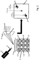
- FIG. 1 An example of a labeling element 2 with nine pixels 1.1 to 1.9 is shown in a top view and a side view.
- the pixels 1.1 to 1.9 were each formed as a structured, circular surface with a linear grid structure using DLIP.
- the top view shows that the alignment of the lattice structures has been selected at different angles / orientations.
- FIG. 1 Above the in Figure 1 top view shown is a corresponding structured surface of a product shown.
- Monochromatic electromagnetic radiation 3 from a laser diode as radiation source 5 is directed onto this structured surface.
- the electromagnetic radiation which is refracted and reflected on the structured surface of the pixels 1.1 to 1.9 forming the marking element 2 impinges on a detector array 4 with which the intensities are detected in a spatially resolved manner.
- Figure 6 can be detected in several diffraction orders. For a check, however, it may be sufficient to consider only one diffraction order, preferably the 1st order.
- pixels 1.1 to 1.9 can look at the detector array 4. After reflection and refraction, pixels 1.1 to 1.9 are mapped by the respective selection of the structure period ⁇ and the angle ⁇ for the alignment of the linear lattice structure of the individual pixels and at least one Figure 6 of the entire labeling element 2 in the 1st diffraction order can be used for a test for authenticity.
- This illustration shows two images 6 of the first diffraction order of the labeling element.
- the illustration (s) 6 correspond to the respectively given identification element 2.
- the radiation with electromagnetic radiation 3 can take place at different angles. Depending on the selected angle, only the position of the entire one changes Figure 6 .
- Grid structure is aligned with respect to an axis of a coordinate system, has an influence on the position of the image of a pixel 1 after the diffraction of electromagnetic radiation on the linear grid structure.
- the angle ⁇ 1 has a value of 90 ° in relation to an x-axis of a coordinate system and the angle ⁇ 2 has a value of 135 ° in relation to the x-axis of a coordinate system.
- the images of the diffraction orders of a pixel 1 with the structure period ⁇ 1 and an angle ⁇ 2 are not arranged on an axis on which the corresponding images of diffraction orders with structure periods ⁇ 1 and ⁇ 2 and the angle ⁇ 1 lie.
- the respective positions of images of pixels after the optical diffraction can thus be influenced by a suitable choice of the structure period ⁇ and / or the angle ⁇ of the individual pixels 1.
- FIG 3 a coordinate system is shown in which a Figure 6 the 1st diffraction order of 10 pixels led to a T-shaped identification element 2.
- Different values for the structure period ⁇ and angle ⁇ have been selected on the individual images of pixels, so that each diffraction is shown corresponding to the respective identification element after the diffraction at the desired position and in this example the identification element 2 has the shape of a "T"" Has.
- the respective choice of the structure period ⁇ and the angle ⁇ of the respective linear grid structure can also be made available with differently designed identification elements 2.
- the structure period ⁇ can be varied in the range 1.2 ⁇ m to 1.6 ⁇ m, the angle ⁇ in the range 24 ° to 52 ° for individual pixels.
- the structure depth of linear lattice structures can be kept constant in the range of 0.001 ⁇ m to 10 ⁇ m and also for all pixels that are assigned to a marking element 2
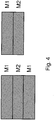
- FIG 4 an arrangement is shown on the left in which a material M2 of another material M1 is covered.
- the illustration on the right shows an arrangement in which a material M2 is covered by another material M1 on two opposite surfaces.
- a material can also be covered on two opposite surfaces by other materials and the other materials are different.
- the materials M1 and M2 are arranged directly one above the other without gaps. However, an arrangement at a distance from one another is also possible.
- the materials can be fixed on the outside with a frame.
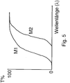
- FIG. 5 The diagram shown shows the differences in the wavelength-dependent transparency for electromagnetic radiation for different materials M1 and M2.
- a wavelength that is identified by the dashed line can therefore preferably be used to form a marking element in a material M2.
- FIGS. 6a and 6b illustrate how structural elements can be formed in the surface of a material M2 by means of DLIP with individual pixels 1.1 to 1.3, in that several partial beams 9 and 9 'can simultaneously be directed locally defined onto the surface of a material M2 by another material M1 covering it.
- Material M1 absorbs at least 80%, preferably almost 100%, of the electromagnetic laser radiation at the selected wavelength ⁇ , whereas the other material M1 does not absorb the electromagnetic radiation with the corresponding wavelength at all, or at most 40%.
- Figures 7a and 7b shows how pixels 1.1 to 1.6 were formed to form a marking element on two oppositely arranged surfaces of a material M2. In this case, they form an almost identical pattern because they have been formed mirrored to the center axis of the material M2. However, an offset arrangement of pixels 1.1 to 1.3, 1.4 to 1.6 and 1.7 to 1.9 is also possible. This is with the representations in Figure 9 (symmetrically on the left on a surface of a material M2 and on the right offset to one another in rows on a surface or one above the other on two surfaces of a material M2).
- Figure 8 it can be seen that individual pixels 1.1 to 1.3 structure elements 10 with a lateral dimension D in an axial direction with 2 ⁇ m to 20 mm with a distance A from one another of 0 nm to 20,000 ⁇ m, preferably from 100 nm to 50 ⁇ m, can be sensibly formed. Individual pixels can be formed with a dimensioning ⁇ in the range from 100 nm to 50 ⁇ m.
Landscapes
- Credit Cards Or The Like (AREA)
- Diffracting Gratings Or Hologram Optical Elements (AREA)
Description
- Die Erfindung betrifft ein Verfahren zur Identifikation von Produkten.
- Nahezu alle Produkte insbesondere Produkte bekannter Marken können heutzutage mit entsprechendem Aufwand kopiert und als Plagiat an den Markt gebracht werden, wodurch erhebliche finanzielle Verluste hervor gerufen werden. Bei solchen Verletzungen entsteht für die Ermittlung und den Nachweis ein erheblicher Aufwand für den ursprünglichen Schöpfer und Hersteller.
- Für einen möglichen Nachweis der Identität bzw. der Herkunft von Produkten sind entsprechende Kennzeichnungen ein geeigneter Weg. Solche Kennzeichnungen sollen unmittelbar am Produkt, möglichst nachahmungssicher, nicht ablösbar und nicht zerstörbar angebracht oder daran ausgebildet sein.
- Üblicherweise werden bisher Hologrammetiketten, Tracertechnologien auf RFID-Basis oder generative Methoden, wie z.B. der Einsatz fluoreszierender Nanopartikel genutzt. Vor allem auf etablierten Hologrammetiketten kommen hochkomplexe Sicherheitselemente, wie z.B. Identigramme, Kinegramme, Computer generierte Hologramme oder Nanogramme zum Einsatz. Damit sind visuelle, sensorische oder mikrokoskopische Möglichkeiten für eine Identifikation gegeben.
- Üblicherweise werden Computer generierte Hologramme mit Hilfe von Mikro- und Nanostrukturen erzeugt, die definierte Wellenfronten erzeugen und somit ein komplexes Beugungsbild als Sicherheitsmerkmal bereitstellen können. Die Herstellung der Mikro- und Nanostrukturen ist üblicherweise nur mit aufwändigen, kostenintensiven und komplizierten Methoden, wie der Elektronenstrahllithografie möglich. Im Allgemeinen kommen aufwändige Algorithmen, wie der iterative Fourier-Transformationsalgorithmus zum Einsatz.
- Als Alternative zu Computer generierten Hologrammen können komplexe, diffraktive Sicherheitselemente (sogenannte Pixogramme) mittels selektiver Oberflächenstrukturierung genutzt werden, die sich sowohl direkt als auch indirekt realisieren lassen. Der Aufwand für die Herstellung der komplexen, diffraktiven Sicherheitselemente ist im Vergleich zu bestehenden mittels Computer generierten Hologrammen sowohl aus finanzieller als auch zeitlicher Sicht deutlich geringer.
- Eine visuelle Prüfung diffraktiver Sicherheitselemente (Pixogramme) erfolgt üblicherweise durch Bestrahlung mit monochromatischer, elektromagnetischer Strahlung.
- Das Dokument
DE 10 2013 105 246 A1 (D1) offenbart ein Verfahren nach dem Oberbegriff des Anspruchs 1. - Es ist daher Aufgabe der Erfindung, Möglichkeiten für die Erkennung und Identifizierung von Produkten und deren Herkunft mit ausreichender Sicherheit anzugeben, wobei dies mit geringem Aufwand und Kosten erreichbar sein soll.
- Erfindungsgemäß wird diese Aufgabe mit einem Verfahren nach Anspruch 1 gelöst. Vorteilhafte Ausgestaltungen und Weiterbildungen der Erfindung können mit in untergeordneten Ansprüchen bezeichneten Merkmalen realisiert werden.
- Bei dem Kennzeichnungselement für Produkte sind auf einer Oberfläche mehrere Pixel mit jeweils einer periodischen Gitterstruktur, insbesondere einer linienförmigen Gitterstruktur, ausgebildet. In einzelnen Pixeln sind Gitterstrukturen mit jeweils einer Strukturperiode Λ und einer Ausrichtung der linienförmigen parallel zueinander ausgerichteten Strukturelemente mit einem Winkel ϕ in Bezug zu einer Bezugsachse so ausgebildet, dass bei Bestrahlung der das Kennzeichnungselement bildenden Pixel mit elektromagnetischer Strahlung auf einem Detektorarray oder einer Fläche eine Abbildung des Kennzeichnungselements durch Abbildungen mindestens einer Ordnung der von Pixeln gebeugten elektromagnetischen Strahlung erfolgt. Die Abbildung kann dann zur Identifikation des jeweiligen Kennzeichnungselements genutzt werden.
- Durch die jeweilige Wahl der Strukturperiode Λ und/oder der Wahl des Winkels ϕ lässt sich die Position der vom jeweiligen Pixel gebeugten und transmittierten oder reflektierten elektromagnetischen Strahlung in mindestens einer Beugungsordnung definiert beeinflussen. Durch geeignete Wahl zumindest eines dieser beiden Parameter kann man die Strukturierung der einzelnen Pixel eines Kennzeichnungselements so wählen, dass das Muster der auf der Oberfläche eines Produktes ausgebildeten Pixel nicht der zweidimensionalen Struktur oder dem Aufbau des Kennzeichnungselements entspricht. Es kann also bei einer direkten Betrachtung nicht als das jeweilige Kennzeichnungselement erkannt werden. Erst nach der Beugung der elektromagnetischen Strahlung an der gitterförmigen Struktur kann das eigentliche Abbild des Kennzeichnungselements mit den Abbildungen von Beugungsordnungen der Pixel als solches erkannt werden.
- Für die Bestrahlung sollte monochromatische Strahlung eingesetzt werden, die bevorzugt von einer Laserdiode auf die mit Pixeln strukturierte Oberfläche emittiert wird. Die Abbildung kann bei Produkten aus optisch transparenten Werkstoffen in Strahlungsrichtung hinter dem Produkt aber auch mit von der Oberfläche reflektierter an den Strukturelementen gebeugter elektromagnetischer Strahlung erfolgen.
- Es können auch Pixel vorhanden sein, die zusätzlich jeweils eine unterschiedliche Strukturtiefe der linienförmigen Strukturelemente aufweisen. Dadurch können Abbildungen erreicht werden, die lokal definiert und den entsprechend ausgebildeten Strukturelementen zugeordnet unterschiedliche Intensitäten aufweisen, was eine weitere Möglichkeit zur Differenzierung von nutzbaren Kennzeichnungselementen und eine Erhöhung der Fälschungssicherheit bewirken kann.
- Die Pixel eines Kennzeichnungselements können und sollten so ausgebildet sein, dass das Kennzeichnungselement als solches an der Oberfläche des Produkts nicht ohne optische Hilfsmittel erkennbar ist. Dabei sollen insbesondere die Pixel nicht ohne Weiteres erkennbar sein. Es sollte also ohne den Einsatz vergrößernder optischer Elemente, insbesondere von optischen Linsen visuell nicht wahrnehmbar sein.
- Die Pixel können kreisförmig oder mehreckig ausgebildet sein. Sie können beispielsweise in einer Reihen- und Spaltenanordnung, bei denen in einzelnen Reihen und Spalten auch unterschiedlich große Anzahlen an Pixeln ausgebildet sein können, angeordnet werden.
- Die einzeln strukturierten Pixel sollten jeweils eine Fläche von maximal 1 mm2 einnehmen. Der strukturierte Gesamtbereich (d.h. die Summe aller Einzelpixel) kann beliebig groß sein.
- Die Pixel sollten eine Strukturperiode Λ im Bereich 0,01 µm - 50 µm und/oder Strukturtiefen im Bereich 0,001 µm -10 µm aufweisen.
- Bei der Bewertung, Prüfung von Abbildungen gebeugter elektromagnetischer Strahlung sollte mindestens elektromagnetische Strahlung einer Beugungsordnung, bevorzugt der 1. Ordnung genutzt werden. Eine Kombination verschiedener Beugungsordnungen ist aber ebenfalls möglich. Vorteilhaft ist es, wenn mindestens eine Strahlungsquelle, ein Detektorarray und/oder ein Display zur Anzeige der Abbildung der Pixel mit der jeweiligen Beugungsordnung eine Einheit bilden. Dadurch kann ein einzelnes kompaktes Gerät geschaffen werden, mit dem eine Überprüfung der Identität eines Kennzeichnungselementes mit einer Vorgabe auf einfache und zeitsparende Art und Weise möglich ist. Dabei kann an einer Oberfläche eine Strahlungsquelle angeordnet sein, mit der elektromagnetische Strahlung auf den mit gitterförmigen Strukturen ausgebildeten Pixeln versehene Oberfläche gerichtet werden. Von dort reflektierte und gebeugte elektromagnetische Strahlung kann dann auf ein auf derselben Seite angeordnetes Detektorarray auftreffen und dort ortsaufgelöst in elektrische Signale gewandelt werden.
- Auf der rückwärtigen Oberfläche kann ein optisches Anzeigeelement vorhanden sein, mit dem die detektierten elektrischen Signale eine Abbildung eines Kennzeichnungselementes ermöglichen, die von einem Nutzer erkannt und mit einer Vorgabe verglichen werden können. Für eine Automatisierung kann zusätzlich eine Mustererkennung integriert sein, mit der eine Überprüfung auf Echtheit elektronisch erreichbar ist. Das Prüfergebnis kann dann visuell oder auch akustisch angezeigt werden.
- Es können auch mehrere Strahlungsquellen unterschiedlicher Wellenlänge zur Überprüfung eingesetzt werden. Diese können elektromagnetische Strahlung auf wellenlängenoptimierte, strukturierte Bereiche eines Kennzeichnungselements richten, so dass in Kombination wellenlängenselektive Sicherheitsmerkmale ausgewertet und bei einer Überprüfung berücksichtigt werden können.
- Die Ausbildung der in Form eines optischen Gitters ausgebildeten Oberflächenstrukturierungen der einzelnen Pixel erfolgt mittels an sich bekannter direkter Laserinterferenzstrukturierung (DLIP) in einfacher kostengünstiger und flexibler Weise. Dabei können auch Prägewerkzeuge, die beispielsweise durch eine Replikation von mit DLIP ausgebildeten Strukturelementen hergestellt werden, eingesetzt werden.
- Mit der Erfindung können komplexe Sicherheitsmerkmale wegen der erreichbaren komplexen Beugungsmuster als Kennzeichnungselement zur Verfügung gestellt werden. Eine Überprüfung beispielsweise auf Echtheit eines Produktes kann mit sehr einfachen optischen Mitteln nahezu an jedem Ort durchgeführt werden. Es können mobile Geräte dafür eingesetzt werden.
- Die Ausbildung eines Kennzeichnungselementes kann unmittelbar auf eine Oberfläche eines Produktes aber auch auf einem Element, das mit dem jeweiligen Produkt verbind bar ist, erfolgen.
- Es besteht auch die Möglichkeit, die das Kennzeichnungselement bildenden Pixel in mindestens einer Oberfläche eines Werkstoffs, der von mindestens einem anderen Werkstoff überdeckt ist oder innerhalb einer Grenzfläche zwischen den Werkstoffen ausgebildet ist, auszubilden. Der andere Werkstoff soll ein kleineres Absorptionsvermögen, insbesondere ein um mindestens 50 % kleineres Absorptionsvermögen für die zur Ausbildung der Pixel eingesetzte Laserstrahlung aufweisen, als der mit dem anderen Werkstoff überdeckte Werkstoff. Ganz besonders bevorzugt sollte der andere Werkstoff die eingesetzte Wellenlänge der Laserstrahlung nicht absorbieren. Durch Auswahl geeigneter Werkstoffpaarungen und einer Wellenlänge der eingesetzten Laserstrahlung kann der optische Brechungsindex lokal definiert im Bereich der Oberfläche des von einem anderen Werkstoff überdeckten Werkstoffs und/oder im Grenzflächenbereich der beiden unterschiedlichen Werkstoffe verändert werden. Es ist dort auch eine Sublimation, also Überführung von insbesondere polymerem Werkstoff erreichbar, bei der polymerer Werkstoff zumindest teilweise in die Gasphase überführt wird. Gas kann dann zwischen den beiden Werkstoffen verbleiben und den gewünschten Effekt erreichen. Es kann auch ein an- oder umschmelzen lokal definiert erreicht werden.
- Insbesondere bei einer Pixelausbildung eines Kennzeichnungselementes mittels direkter Laserstrahlinterferenznutzung kann eine geeignete Fokussierung der eingesetzten Teilstrahlen auf die Oberfläche des Werkstoffs, der von einem anderen Werkstoff überdeckt ist, oder eine Grenzfläche die von dem einen und einem anderen Werkstoff gebildet ist, in die entsprechende Ebene gewählt werden, um sehr feine filigrane Strukturen eines Kennzeichnungselmentes ausbilden zu können.
- Der mindestens eine andere Werkstoff sollte ein Polymer, insbesondere eine Polymerfolie sein. Die Werkstoffe sollten stoffschlüssig, bevorzugt mit einem organischen Binder verbunden sein.
- Demzufolge kann ein Teil aus einem Werkstoff gebildet sein, das an zwei gegenüberliegend angeordneten Oberflächen von jeweils einem anderen Werkstoff überdeckt ist. Die anderen Werkstoffe können gleich aber auch unterschiedlich sein.
- Als polymere Werkstoffe kommen Paarungen unterschiedlicher Polymere infrage. So können Polymethylmethacrylat (PMMA) mit dem anderen Werkstoff Polycarbonat (PC),PMMA mit Polypropylen (PP) sowie PMMA mit Polyethylen (PET) bei einer Wellenlänge der Laserstrahlung von 266 nm oder 263 nm, PMMA und Polyimid (PI) sowie PMMA und Polyetheretherketon (PEEK) PET und PI sowie PP und PI bei einer Wellenlänge von 355 nm entsprechend bearbeitet werden. Dabei ist das jeweils erstgenannte Polymer, der andere Werkstoff, der einen Werkstoff überdeckt.
- Nachfolgend soll die Erfindung beispielhaft näher erläutert werden.
- Dabei zeigen:
- Figur 1
- in schematischer Form ein mit Pixeln ausgebildetes Beispiel eines Kennzeichnungselementes und einen Aufbau zur Überprüfung der Identität des Kennzeichnungselements;
- Figuren 2a-c
- in schematischer Form den Einfluss unterschiedlicher Strukturperioden Λ und Winkel ϕ der Strukturorientierung auf eine Position der an einem Pixel gebeugten Abbildung des jeweiligen Pixels;
- Figur 3
- die Abbildung von 10 Pixeln, die ein T-förmiges Kennzeichnungselement bilden, in der ersten Beugungsordnung;
- Figur4
- Beispiele bei denen ein Werkstoff an einer oder an beiden gegenüberliegend angeordneten Oberflächen von einem anderen Werkstoff überdeckt ist;
- Figur 5
- ein Diagramm, das die optische Transparenz und daher umgekehrt das Absorptionsverhalten in Abhängigkeit der jeweiligen Wellenlänge für einen Werkstoff M1 und einen anderen Werkstoff M2 wieder gibt;
- Figur 6a + b
- eine schematische Darstellung wie zwei Teilstrahlen zur Ausbildung von Pixeln eines Kennzeichnungselmentes auf die Oberfläche eines Werkstoffs M1 durch einen anderen Werkstoff M2 gerichtet sind;
- Figur 7a + b
- in schematischer Form eine Ausbildung von Strukturelementen an zwei gegenüberliegenden Oberflächen eines Werkstoffs, der an beiden gegenüberliegend angeordneten Oberflächen von einem anderen Werkstoff überdeckt ist;
- Figur 8
- in schematischer Darstellung mittels direktes Laserinterferenzstrukturieren (DLIP) ausbildbarer Strukturelemente für ein Kennzeichnungselement mit geeigneter Dimensionierung und
- Figur 9
- in schematischer Darstellung Möglichkeiten für eine Anordnung einzelner Strukturelemente mit Pixeln, die mittels DLIP für eine Ausbildung eines Kenzeichnungselements genutzt werden können.
- In
Figur 1 ist ein Beispiel eines Kennzeichnungselementes 2 mit neun Pixeln 1.1 bis 1.9 in einer Draufsicht und einer Seitenansicht gezeigt. Die Pixel 1.1 bis 1.9 wurden jeweils als strukturierte, kreisförmige Oberfläche mit jeweils einer linienförmigen Gitterstruktur mittels DLIP ausgebildet. Aus der Draufsicht geht hervor, dass die Ausrichtung der Gitterstrukturen in verschiedenen Winkeln/Orientierungen gewählt worden ist. - Oberhalb der in
Figur 1 gezeigten Draufsicht ist eine entsprechend strukturierte Oberfläche eines Produktes gezeigt. Auf diese strukturierte Oberfläche wird monochromatische elektromagnetische Strahlung 3 von einer Laserdiode als Strahlungsquelle 5 gerichtet. Die an der strukturierten Oberfläche der das Kennzeichnungselement 2 bildenden Pixel 1. 1 bis 1.9 gebrochenen und reflektierte elektromagnetische Strahlung trifft auf ein Detektorarray 4 auf, mit dem die Intensitäten ortsaufgelöst erfasst werden. Wie man der oberen Darstellung vonFigur 1 entnehmen kann, können Abbildungen 6 in mehreren Beugungsordnungen so detektiert werden. Für eine Überprüfung kann es aber ausreichen lediglich eine Beugungsordnung, bevorzugt die 1. Ordnung zu berücksichtigen. - Mit der rechten Darstellung von
Figur 1 wird deutlich, wie dieAbbildung 6 der Pixel 1.1 bis 1.9 am Detektorarray 4 aussehen kann. Dabei erfolgt nach Reflexion und Brechung eine Abbildung der Pixel 1.1 bis 1.9 durch die jeweilige Auswahl der Strukturperiode Λ und dem Winkel ϕ für die Ausrichtung der linienförmigen Gitterstruktur der einzelnen Pixel und es kann mindestens eineAbbildung 6 des gesamten Kennzeichnungselements 2 in 1. Beugungsordnung für eine Prüfung auf Echtheit herangezogen werden. In dieser Darstellung sind zwei Abbildungen 6 der jeweils 1. Beugungsordnung des Kennzeichnungselements dargestellt. - Die Abbildung(en) 6 entsprechen dem jeweils vorgegebenen Kenzeichnungselement 2. Die Bestrahlung mit elektromagnetischer Strahlung 3 kann in verschiedenen Winkeln erfolgen. Je nach gewähltem Winkel verändert sich lediglich die Position der gesamten
Abbildung 6 . - Mit den aus den
Figuren 2a und 2b entnehmbaren Darstellungen wird verdeutlicht welchen Einfluss eine veränderte Strukturperiode Λ auf eine Position einer Abbildung einer Ordnung hat. So war die Strukturperiode Λ1 größer als die Strukturperiode Λ2. Der Abstand der Abbildung eines Pixels 1 nach der Brechung an der Gitterstruktur von einem Nullpunkt eines kartesischen Koordinatensystems verändert sich also in Abhängigkeit der jeweiligen Strukturperiode Λ in einer Achsrichtung. - Mit
Figur 2c wird deutlich, dass auch der Winkel ϕ mit dem die linienförmige - Gitterstruktur in Bezug zu einer Achse eines Koordinatensystems ausgerichtet ausgebildet worden ist, einen Einfluss auf die Position der Abbildung eines Pixels 1 nach der Beugung elektromagnetischer Strahlung an der linienförmigen Gitterstruktur hat. In den Darstellung nach
Figur 2a bis 2c hat der Winkel ϕ1 einen Wert von 90 ° in Bezug zu einer x-Achse eines Koordinatensystems und der Winkel ϕ2 einen Wert von 135° in Bezug zur x-Achse eines Koordinatensystems. Daraus ergibt sich, dass die Abbildungen der Beugungsordnungen eines Pixels 1 mit der Strukturperiode Λ1 und einem Winkel ϕ2 nicht auf einer Achse angeordnet sind, auf der die entsprechenden Abbildungen von Beugungsordnungen mit Strukturperioden Λ1 und Λ2 und dem Winkel ϕ1 liegen. Es kann also eine Beeinflussung der jeweiligen Positionen von Abbildungen von Pixeln nach der optischen Beugung durch geeignete Wahl der Strukturperiode Λ und/oder des Winkels ϕ der einzelnen Pixel 1 genommen werden. - In
Figur 3 ist ein Koordinatensystem gezeigt, bei dem eineAbbildung 6 der 1. Beugungsordnung von 10 Pixeln zu einem T-Förmigen Kennzeichnungselement 2 führte. An den einzelnen Abbildungen von Pixeln sind jeweils unterschiedliche Werte für die Strukturperiode Λ und Winkel ϕ gewählt worden, so dass jedes Pixel nach der Beugung an der gewünschten Position dem jeweiligen Kennzeichnungselement entsprechend zugeordnet abgebildet wird und bei diesem Beispiel das Kennzeichnungselement 2 die Form eines "T" hat. Selbstverständlich können durch Variation der Anzahl an Pixeln deren Anordnung auf einer Oberfläche, der jeweiligen Wahl der Strukturperiode Λ und des Winkels ϕ der jeweiligen linienförmigen Gitterstruktur auch unterschiedlichst gestaltete Kennzeichnungselemente 2 zu Verfügung gestellt werden. - So kann bei dem gezeigten Beispiel die Strukturperiode Λ im Bereich 1,2 µm bis 1,6 µm, der Winkel ϕ im Bereich 24 ° bis 52° jeweils für einzelne Pixel variiert werden. Die Strukturtiefe von linienförmigen Gitterstrukturen kann im Bereich 0,001 µm bis 10 µm und dabei auch bei allen Pixeln, die einem Kennzeichnungselement 2 zugeordnet sind, konstant gehalten werden
- In
Figur 4 ist links eine Anordnung gezeigt, bei der ein Werkstoff M2 von einem anderen Werkstoff M1 überdeckt ist. Die rechte Darstellung zeigt eine Anordnung bei der ein Werkstoff M2 von einem anderen Werkstoff M1 an zwei gegenüberliegenden Oberflächen überdeckt ist. Es kann auch ein Werkstoff an zwei gegenüberliegenden Oberflächen von anderen Werkstoffen überdeckt sein und dabei die anderen Werkstoffe unterschiedlich sind. InFigur 4 sind die Werkstoffe M1 und M2 direkt übereinander spaltfrei angeordnet. Es ist aber auch eine Anordnung mit einem Abstand zueinander möglich. Dabei können die Werkstoffe an Außenseiten mit einem Rahmen fixiert sein. - Das in
Figur 5 gezeigte Diagramm gibt die Unterschiede der wellenlängenabhängigen Transparenz für elektromagnetische Strahlung für unterschiedliche Werkstoffe M1 und M2 wieder. Bevorzugt kann also eine Wellenlänge, die mit der gestrichelten Linie kenntlich gemacht ist, zur Ausbildung eines Kennzeichnungselements in einem Werkstoff M2 genutzt werden. - Die
Figuren 6a und6b verdeutlichen, wie Strukturelemente in der Oberfläche eines Werkstoffs M2 mittels DLIP mit einzelnen Pixeln 1.1 bis 1.3 ausgebildet werden können, indem gleichzeitig mehrere Teilstrahlen 9 und 9' lokal definiert auf die Oberfläche eines Werkstoffs M2 durch einen diesen überdeckenden anderen Werkstoff M1 gerichtet werden können. Dabei absorbiert der Werkstoff M1 die elektromagnetische Laserstrahlung bei der gewählten Wellenlänge λ zu mindestens 80 %, bevorzugt nahezu 100 %, wohingegen der andere Werkstoff M1 die elektromagnetische Strahlung mit der entsprechenden Wellenlänge gar nicht oder zu maximal 40 % absorbiert. - In
Figuren 7a und7b ist gezeigt, wie Pixel 1.1 bis 1.6 zur Ausbildung eines Kennzeichnungselements an zwei gegenüberliegend angeordneten Oberflächen eines Werkstoffs M2 ausgebildet worden sind. In diesem Fall bilden sie ein nahezu identisches Muster, da sie gespiegelt zur Mittenachse des Werkstoffs M2 ausgebildet worden sind. Es ist aber auch eine versetzte Anordnung von Pixeln 1.1 bis 1.3, 1.4 bis 1.6 und 1.7 bis 1.9 möglich. Dies ist mit den Darstellungen inFigur 9 (links symmetrisch an einer Oberfläche eines Werkstoffs M2 und rechts versetzt zueinander in Reihen an einer Oberfläche oder an übereinander an zwei Oberflächen eines Werkstoffs M2) angedeutet.Figur 8 kann man entnehmen, dass einzelne Pixel 1.1 bis 1.3 Strukturelemente 10 mit einer lateralen Dimensionierung D in eine Achsrichtung mit 2 µm bis 20 mm mit einem Abstand A zueinander von 0 nm bis 20.000µm, bevorzugt von 100 nm bis 50 µm sinnvoll ausgebildet werden können. Einzelne Pixel können mit einer Dimensionierung Λ im Bereich 100 nm bis 50 µm ausgebildet werden.
Claims (5)
- Verfahren zur Identifikation für Produkte mit einem Kennzeichnungselement, bei dem auf einer Oberfläche mehrere Pixel (1.1 bis 1.x) mit periodischen Gitterstrukturen, insbesondere linienförmige Gitterstrukturen, mittels direkter Laserinterferenzstrukturierung als Kennzeichnungselement ausgebildet sind, und
in einzelnen Pixeln (1.1 bis 1.x) Gitterstrukturen mit jeweils einer Strukturperiode Λ und einer Ausrichtung der insbesondere linienförmigen parallel zueinander ausgerichteten Strukturelemente mit einem Winkel ϕ in Bezug zu einer Bezugsachse so ausgebildet sind, wobei bei Bestrahlung der das Kennzeichnungselement (2) bildenden Pixel (1.1 bis 1.x) mit elektromagnetischer Strahlung (3), bevorzugt monochromatischer elektromagnetischer Strahlung von mindestens einer Strahlungsquelle Abbildungen mindestens einer Beugungsordnung der von Pixeln (1.1 bis 1.x) gebeugten elektromagnetischen Strahlung (3) erhalten werden, und
auf einem Detektorarray (4) die Abbildungen des Kennzeichnungselements (2) der mindestens einen Beugungsordnung erfolgt und diese zur Identifikation des jeweiligen Kennzeichnungselements (2) nutzbar ist. - Verfahren nach Anspruch 1, dadurch gekennzeichnet, dass mehrere Strahlungsquellen unterschiedlicher Wellenlängen für die Bestrahlung eingesetzt werden.
- Verfahren nach Anspruch 1 oder 2, dadurch gekennzeichnet, dass elektromagnetische Strahlung mehrerer Wellenlängen auf wellenlängenoptimierte strukturierte Bereiche richten, so dass wellenlängenselektive Sicherheitsmerkmale ausgewertet werden.
- Verfahren nach einem der vorhergehenden Ansprüche, dadurch gekennzeichnet, dass mit einem optischen Anzeigeelement eine von einem Nutzer erkennbare Abbildung eines Kennzeichnungselements (2) erhalten wird, die mit einer Vorgabe verglichen wird.
- Verfahren nach einem der vorhergehenden Ansprüche, dadurch gekennzeichnet, dass mit einer Mustererkennung eine Überprüfung in Echtzeit erfolgt, Wobei bevorzugt das Prüfergebnis der Mustererkennung visuell oder optisch angezeigt wird.
Applications Claiming Priority (2)
| Application Number | Priority Date | Filing Date | Title |
|---|---|---|---|
| DE102016210119 | 2016-06-08 | ||
| DE102016215160.6A DE102016215160A1 (de) | 2016-06-08 | 2016-08-15 | Kennzeichnungselement für Produkte |
Publications (3)
| Publication Number | Publication Date |
|---|---|
| EP3254862A1 EP3254862A1 (de) | 2017-12-13 |
| EP3254862B1 EP3254862B1 (de) | 2019-02-27 |
| EP3254862B3 true EP3254862B3 (de) | 2020-04-29 |
Family
ID=59053914
Family Applications (1)
| Application Number | Title | Priority Date | Filing Date |
|---|---|---|---|
| EP17174013.7A Active EP3254862B3 (de) | 2016-06-08 | 2017-06-01 | Verfahren zur identifikation für produkte |
Country Status (1)
| Country | Link |
|---|---|
| EP (1) | EP3254862B3 (de) |
Family Cites Families (3)
| Publication number | Priority date | Publication date | Assignee | Title |
|---|---|---|---|---|
| DE102011014114B3 (de) * | 2011-03-15 | 2012-05-10 | Ovd Kinegram Ag | Mehrschichtkörper und Verfahren zur Herstellung eines Mehrschichtkörpers |
| DE102012105571B4 (de) * | 2012-06-26 | 2017-03-09 | Ovd Kinegram Ag | Dekorelement sowie Sicherheitsdokument mit einem Dekorelement |
| DE102013105246B4 (de) * | 2013-05-22 | 2017-03-23 | Leonhard Kurz Stiftung & Co. Kg | Optisch variables Element |
-
2017
- 2017-06-01 EP EP17174013.7A patent/EP3254862B3/de active Active
Also Published As
| Publication number | Publication date |
|---|---|
| EP3254862B1 (de) | 2019-02-27 |
| EP3254862A1 (de) | 2017-12-13 |
Similar Documents
| Publication | Publication Date | Title |
|---|---|---|
| EP2867031B1 (de) | Sicherheitselement mit beugungsstrukturen aufweisenden mikrostrukturen sowie verfahren zur herstellung und verifikation | |
| EP1237435B1 (de) | Coin having diffraction structures | |
| EP2155963B8 (de) | Durchsichtssicherheitselement | |
| EP1599345B1 (de) | Sicherheitselement mit einer gitterstruktur | |
| EP3488389B1 (de) | Vorrichtung und verfahren zur erzeugung und detektieren einer fälschungssicheren identifikation | |
| EP3423286B1 (de) | Sicherheitsgegenstand mit dynamischem und statischem fenstersicherheitsmerkmal und verfahren zur herstellung | |
| DE102016215160A1 (de) | Kennzeichnungselement für Produkte | |
| DE102005003958A1 (de) | Sicherheitselement und Verfahren zu seiner Herstellung | |
| EP2029371B1 (de) | Refraktives durchsichtssicherheitselement | |
| DE112016000676T5 (de) | Winkelabhängige Effekte erzeugende diffraktive Vorrichtung | |
| EP1676156B1 (de) | Optisch variable beugungsstruktur und verfahren zu ihrer herstellung | |
| DE102014217099B4 (de) | Verfahren zur Herstellung eines Sicherheitshologramms mit einem Transmissionsvolumenhologramm in Kontaktkopie | |
| EP2782765A1 (de) | Sicherheitseinrichtung | |
| EP1521680B1 (de) | Verfahren zum erzeugen eines gitterbildes, gitterbild und sicherheitsdokument | |
| WO2017109120A1 (de) | Verfahren zum herstellen eines sicherheitsdokumentes und sicherheitsdokument | |
| DE19949945A1 (de) | Datenträger mit Echtheitsmerkmalen und Herstellverfahren hierfür | |
| DE102018217560A1 (de) | Beugendes Sicherheitselement | |
| EP3254862B3 (de) | Verfahren zur identifikation für produkte | |
| EP2895921A1 (de) | Master für die herstellung eines volumenreflexions-hologramms mit verbesserter marker-ausbildung | |
| EP3039491B1 (de) | Verfahren zum dezentralen markieren eines sicherheitsdokuments | |
| EP3648983B1 (de) | Optisch variable sicherheitsanordnung | |
| DE102020004967A1 (de) | Retroreflektierendes Element mit einem Sicherheitselement | |
| DE60124283T2 (de) | Optischer Datenträger mit einem auf optischer Beugung basierenden Code, und zugehöriges Lesegerät | |
| EP2558303A1 (de) | Selbstverifizierendes optisches sicherheitselement | |
| DE102015215743B4 (de) | Kennzeichnungselement auf einer Oberfläche eines Bauteils |
Legal Events
| Date | Code | Title | Description |
|---|---|---|---|
| PUAI | Public reference made under article 153(3) epc to a published international application that has entered the european phase |
Free format text: ORIGINAL CODE: 0009012 |
|
| STAA | Information on the status of an ep patent application or granted ep patent |
Free format text: STATUS: THE APPLICATION HAS BEEN PUBLISHED |
|
| AK | Designated contracting states |
Kind code of ref document: A1 Designated state(s): AL AT BE BG CH CY CZ DE DK EE ES FI FR GB GR HR HU IE IS IT LI LT LU LV MC MK MT NL NO PL PT RO RS SE SI SK SM TR |
|
| AX | Request for extension of the european patent |
Extension state: BA ME |
|
| STAA | Information on the status of an ep patent application or granted ep patent |
Free format text: STATUS: REQUEST FOR EXAMINATION WAS MADE |
|
| 17P | Request for examination filed |
Effective date: 20180516 |
|
| RBV | Designated contracting states (corrected) |
Designated state(s): AL AT BE BG CH CY CZ DE DK EE ES FI FR GB GR HR HU IE IS IT LI LT LU LV MC MK MT NL NO PL PT RO RS SE SI SK SM TR |
|
| GRAP | Despatch of communication of intention to grant a patent |
Free format text: ORIGINAL CODE: EPIDOSNIGR1 |
|
| STAA | Information on the status of an ep patent application or granted ep patent |
Free format text: STATUS: GRANT OF PATENT IS INTENDED |
|
| RIC1 | Information provided on ipc code assigned before grant |
Ipc: B42D 25/328 20140101AFI20180814BHEP |
|
| INTG | Intention to grant announced |
Effective date: 20180917 |
|
| TPAC | Observations filed by third parties |
Free format text: ORIGINAL CODE: EPIDOSNTIPA |
|
| GRAS | Grant fee paid |
Free format text: ORIGINAL CODE: EPIDOSNIGR3 |
|
| GRAA | (expected) grant |
Free format text: ORIGINAL CODE: 0009210 |
|
| STAA | Information on the status of an ep patent application or granted ep patent |
Free format text: STATUS: THE PATENT HAS BEEN GRANTED |
|
| AK | Designated contracting states |
Kind code of ref document: B1 Designated state(s): AL AT BE BG CH CY CZ DE DK EE ES FI FR GB GR HR HU IE IS IT LI LT LU LV MC MK MT NL NO PL PT RO RS SE SI SK SM TR |
|
| REG | Reference to a national code |
Ref country code: GB Ref legal event code: FG4D Free format text: NOT ENGLISH |
|
| REG | Reference to a national code |
Ref country code: CH Ref legal event code: EP |
|
| REG | Reference to a national code |
Ref country code: AT Ref legal event code: REF Ref document number: 1100774 Country of ref document: AT Kind code of ref document: T Effective date: 20190315 |
|
| REG | Reference to a national code |
Ref country code: IE Ref legal event code: FG4D Free format text: LANGUAGE OF EP DOCUMENT: GERMAN |
|
| REG | Reference to a national code |
Ref country code: DE Ref legal event code: R096 Ref document number: 502017000814 Country of ref document: DE |
|
| REG | Reference to a national code |
Ref country code: NL Ref legal event code: MP Effective date: 20190227 |
|
| REG | Reference to a national code |
Ref country code: LT Ref legal event code: MG4D |
|
| PG25 | Lapsed in a contracting state [announced via postgrant information from national office to epo] |
Ref country code: LT Free format text: LAPSE BECAUSE OF FAILURE TO SUBMIT A TRANSLATION OF THE DESCRIPTION OR TO PAY THE FEE WITHIN THE PRESCRIBED TIME-LIMIT Effective date: 20190227 Ref country code: NO Free format text: LAPSE BECAUSE OF FAILURE TO SUBMIT A TRANSLATION OF THE DESCRIPTION OR TO PAY THE FEE WITHIN THE PRESCRIBED TIME-LIMIT Effective date: 20190527 Ref country code: SE Free format text: LAPSE BECAUSE OF FAILURE TO SUBMIT A TRANSLATION OF THE DESCRIPTION OR TO PAY THE FEE WITHIN THE PRESCRIBED TIME-LIMIT Effective date: 20190227 Ref country code: PT Free format text: LAPSE BECAUSE OF FAILURE TO SUBMIT A TRANSLATION OF THE DESCRIPTION OR TO PAY THE FEE WITHIN THE PRESCRIBED TIME-LIMIT Effective date: 20190627 Ref country code: FI Free format text: LAPSE BECAUSE OF FAILURE TO SUBMIT A TRANSLATION OF THE DESCRIPTION OR TO PAY THE FEE WITHIN THE PRESCRIBED TIME-LIMIT Effective date: 20190227 Ref country code: NL Free format text: LAPSE BECAUSE OF FAILURE TO SUBMIT A TRANSLATION OF THE DESCRIPTION OR TO PAY THE FEE WITHIN THE PRESCRIBED TIME-LIMIT Effective date: 20190227 |
|
| PG25 | Lapsed in a contracting state [announced via postgrant information from national office to epo] |
Ref country code: HR Free format text: LAPSE BECAUSE OF FAILURE TO SUBMIT A TRANSLATION OF THE DESCRIPTION OR TO PAY THE FEE WITHIN THE PRESCRIBED TIME-LIMIT Effective date: 20190227 Ref country code: GR Free format text: LAPSE BECAUSE OF FAILURE TO SUBMIT A TRANSLATION OF THE DESCRIPTION OR TO PAY THE FEE WITHIN THE PRESCRIBED TIME-LIMIT Effective date: 20190528 Ref country code: LV Free format text: LAPSE BECAUSE OF FAILURE TO SUBMIT A TRANSLATION OF THE DESCRIPTION OR TO PAY THE FEE WITHIN THE PRESCRIBED TIME-LIMIT Effective date: 20190227 Ref country code: IS Free format text: LAPSE BECAUSE OF FAILURE TO SUBMIT A TRANSLATION OF THE DESCRIPTION OR TO PAY THE FEE WITHIN THE PRESCRIBED TIME-LIMIT Effective date: 20190627 Ref country code: BG Free format text: LAPSE BECAUSE OF FAILURE TO SUBMIT A TRANSLATION OF THE DESCRIPTION OR TO PAY THE FEE WITHIN THE PRESCRIBED TIME-LIMIT Effective date: 20190527 Ref country code: RS Free format text: LAPSE BECAUSE OF FAILURE TO SUBMIT A TRANSLATION OF THE DESCRIPTION OR TO PAY THE FEE WITHIN THE PRESCRIBED TIME-LIMIT Effective date: 20190227 |
|
| PLCP | Request for limitation filed |
Free format text: ORIGINAL CODE: EPIDOSNLIM1 |
|
| REG | Reference to a national code |
Ref country code: DE Ref legal event code: R055 Ref document number: 502017000814 Country of ref document: DE |
|
| PLCQ | Request for limitation of patent found admissible |
Free format text: ORIGINAL CODE: 0009231 |
|
| PG25 | Lapsed in a contracting state [announced via postgrant information from national office to epo] |
Ref country code: AL Free format text: LAPSE BECAUSE OF FAILURE TO SUBMIT A TRANSLATION OF THE DESCRIPTION OR TO PAY THE FEE WITHIN THE PRESCRIBED TIME-LIMIT Effective date: 20190227 Ref country code: ES Free format text: LAPSE BECAUSE OF FAILURE TO SUBMIT A TRANSLATION OF THE DESCRIPTION OR TO PAY THE FEE WITHIN THE PRESCRIBED TIME-LIMIT Effective date: 20190227 Ref country code: CZ Free format text: LAPSE BECAUSE OF FAILURE TO SUBMIT A TRANSLATION OF THE DESCRIPTION OR TO PAY THE FEE WITHIN THE PRESCRIBED TIME-LIMIT Effective date: 20190227 Ref country code: DK Free format text: LAPSE BECAUSE OF FAILURE TO SUBMIT A TRANSLATION OF THE DESCRIPTION OR TO PAY THE FEE WITHIN THE PRESCRIBED TIME-LIMIT Effective date: 20190227 Ref country code: IT Free format text: LAPSE BECAUSE OF FAILURE TO SUBMIT A TRANSLATION OF THE DESCRIPTION OR TO PAY THE FEE WITHIN THE PRESCRIBED TIME-LIMIT Effective date: 20190227 Ref country code: RO Free format text: LAPSE BECAUSE OF FAILURE TO SUBMIT A TRANSLATION OF THE DESCRIPTION OR TO PAY THE FEE WITHIN THE PRESCRIBED TIME-LIMIT Effective date: 20190227 Ref country code: EE Free format text: LAPSE BECAUSE OF FAILURE TO SUBMIT A TRANSLATION OF THE DESCRIPTION OR TO PAY THE FEE WITHIN THE PRESCRIBED TIME-LIMIT Effective date: 20190227 Ref country code: SK Free format text: LAPSE BECAUSE OF FAILURE TO SUBMIT A TRANSLATION OF THE DESCRIPTION OR TO PAY THE FEE WITHIN THE PRESCRIBED TIME-LIMIT Effective date: 20190227 |
|
| LIM1 | Request for limitation found admissible |
Free format text: SEQUENCE NO: 1; FILED DURING OPPOSITION PERIOD Filing date: 20191016 Effective date: 20191016 |
|
| REG | Reference to a national code |
Ref country code: DE Ref legal event code: R097 Ref document number: 502017000814 Country of ref document: DE |
|
| PG25 | Lapsed in a contracting state [announced via postgrant information from national office to epo] |
Ref country code: PL Free format text: LAPSE BECAUSE OF FAILURE TO SUBMIT A TRANSLATION OF THE DESCRIPTION OR TO PAY THE FEE WITHIN THE PRESCRIBED TIME-LIMIT Effective date: 20190227 Ref country code: SM Free format text: LAPSE BECAUSE OF FAILURE TO SUBMIT A TRANSLATION OF THE DESCRIPTION OR TO PAY THE FEE WITHIN THE PRESCRIBED TIME-LIMIT Effective date: 20190227 |
|
| PLBE | No opposition filed within time limit |
Free format text: ORIGINAL CODE: 0009261 |
|
| STAA | Information on the status of an ep patent application or granted ep patent |
Free format text: STATUS: NO OPPOSITION FILED WITHIN TIME LIMIT |
|
| PLCO | Limitation procedure: reply received to communication from examining division + time limit |
Free format text: ORIGINAL CODE: EPIDOSNLIR3 |
|
| PG25 | Lapsed in a contracting state [announced via postgrant information from national office to epo] |
Ref country code: MC Free format text: LAPSE BECAUSE OF FAILURE TO SUBMIT A TRANSLATION OF THE DESCRIPTION OR TO PAY THE FEE WITHIN THE PRESCRIBED TIME-LIMIT Effective date: 20190227 |
|
| 26N | No opposition filed |
Effective date: 20191128 |
|
| PLCR | Communication despatched that request for limitation of patent was allowed |
Free format text: ORIGINAL CODE: 0009245 |
|
| REG | Reference to a national code |
Ref country code: DE Ref legal event code: R056 Ref document number: 502017000814 Country of ref document: DE |
|
| PG25 | Lapsed in a contracting state [announced via postgrant information from national office to epo] |
Ref country code: SI Free format text: LAPSE BECAUSE OF FAILURE TO SUBMIT A TRANSLATION OF THE DESCRIPTION OR TO PAY THE FEE WITHIN THE PRESCRIBED TIME-LIMIT Effective date: 20190227 |
|
| PLCN | Payment of fee for limitation of patent |
Free format text: ORIGINAL CODE: EPIDOSNRAL3 |
|
| PUAM | (expected) publication of b3 document |
Free format text: ORIGINAL CODE: 0009410 |
|
| REG | Reference to a national code |
Ref country code: BE Ref legal event code: MM Effective date: 20190630 |
|
| STAA | Information on the status of an ep patent application or granted ep patent |
Free format text: STATUS: THE PATENT HAS BEEN LIMITED |
|
| PG25 | Lapsed in a contracting state [announced via postgrant information from national office to epo] |
Ref country code: TR Free format text: LAPSE BECAUSE OF FAILURE TO SUBMIT A TRANSLATION OF THE DESCRIPTION OR TO PAY THE FEE WITHIN THE PRESCRIBED TIME-LIMIT Effective date: 20190227 |
|
| REG | Reference to a national code |
Ref country code: CH Ref legal event code: AELM |
|
| PG25 | Lapsed in a contracting state [announced via postgrant information from national office to epo] |
Ref country code: IE Free format text: LAPSE BECAUSE OF NON-PAYMENT OF DUE FEES Effective date: 20190601 |
|
| PG25 | Lapsed in a contracting state [announced via postgrant information from national office to epo] |
Ref country code: BE Free format text: LAPSE BECAUSE OF NON-PAYMENT OF DUE FEES Effective date: 20190630 Ref country code: LU Free format text: LAPSE BECAUSE OF NON-PAYMENT OF DUE FEES Effective date: 20190601 |
|
| REG | Reference to a national code |
Ref country code: CH Ref legal event code: PL |
|
| PG25 | Lapsed in a contracting state [announced via postgrant information from national office to epo] |
Ref country code: LI Free format text: LAPSE BECAUSE OF NON-PAYMENT OF DUE FEES Effective date: 20200630 Ref country code: CH Free format text: LAPSE BECAUSE OF NON-PAYMENT OF DUE FEES Effective date: 20200630 |
|
| PG25 | Lapsed in a contracting state [announced via postgrant information from national office to epo] |
Ref country code: CY Free format text: LAPSE BECAUSE OF FAILURE TO SUBMIT A TRANSLATION OF THE DESCRIPTION OR TO PAY THE FEE WITHIN THE PRESCRIBED TIME-LIMIT Effective date: 20190227 |
|
| PG25 | Lapsed in a contracting state [announced via postgrant information from national office to epo] |
Ref country code: HU Free format text: LAPSE BECAUSE OF FAILURE TO SUBMIT A TRANSLATION OF THE DESCRIPTION OR TO PAY THE FEE WITHIN THE PRESCRIBED TIME-LIMIT; INVALID AB INITIO Effective date: 20170601 Ref country code: MT Free format text: LAPSE BECAUSE OF FAILURE TO SUBMIT A TRANSLATION OF THE DESCRIPTION OR TO PAY THE FEE WITHIN THE PRESCRIBED TIME-LIMIT Effective date: 20190227 |
|
| PG25 | Lapsed in a contracting state [announced via postgrant information from national office to epo] |
Ref country code: MK Free format text: LAPSE BECAUSE OF FAILURE TO SUBMIT A TRANSLATION OF THE DESCRIPTION OR TO PAY THE FEE WITHIN THE PRESCRIBED TIME-LIMIT Effective date: 20190227 |
|
| P01 | Opt-out of the competence of the unified patent court (upc) registered |
Effective date: 20230524 |
|
| PGFP | Annual fee paid to national office [announced via postgrant information from national office to epo] |
Ref country code: FR Payment date: 20230628 Year of fee payment: 7 Ref country code: DE Payment date: 20230630 Year of fee payment: 7 |
|
| REG | Reference to a national code |
Ref country code: AT Ref legal event code: MM01 Ref document number: 1100774 Country of ref document: AT Kind code of ref document: T Effective date: 20220601 |
|
| PG25 | Lapsed in a contracting state [announced via postgrant information from national office to epo] |
Ref country code: AT Free format text: LAPSE BECAUSE OF NON-PAYMENT OF DUE FEES Effective date: 20220601 |
|
| PGFP | Annual fee paid to national office [announced via postgrant information from national office to epo] |
Ref country code: GB Payment date: 20230622 Year of fee payment: 7 |