EP2859396B1 - Verfahren für abgetastete beleuchtung - Google Patents
Verfahren für abgetastete beleuchtung Download PDFInfo
- Publication number
- EP2859396B1 EP2859396B1 EP13801133.3A EP13801133A EP2859396B1 EP 2859396 B1 EP2859396 B1 EP 2859396B1 EP 13801133 A EP13801133 A EP 13801133A EP 2859396 B1 EP2859396 B1 EP 2859396B1
- Authority
- EP
- European Patent Office
- Prior art keywords
- camera
- substrate
- pixels
- rows
- light
- Prior art date
- Legal status (The legal status is an assumption and is not a legal conclusion. Google has not performed a legal analysis and makes no representation as to the accuracy of the status listed.)
- Active
Links
- 238000005286 illumination Methods 0.000 title claims description 108
- 238000000034 method Methods 0.000 title claims description 97
- 238000003384 imaging method Methods 0.000 claims description 156
- 239000000758 substrate Substances 0.000 claims description 156
- 230000033001 locomotion Effects 0.000 claims description 41
- 230000003287 optical effect Effects 0.000 claims description 29
- 230000007246 mechanism Effects 0.000 claims description 24
- 150000007523 nucleic acids Chemical class 0.000 description 63
- 102000039446 nucleic acids Human genes 0.000 description 61
- 108020004707 nucleic acids Proteins 0.000 description 61
- 238000012163 sequencing technique Methods 0.000 description 61
- 238000005096 rolling process Methods 0.000 description 31
- 238000010586 diagram Methods 0.000 description 26
- 239000000523 sample Substances 0.000 description 23
- 125000003729 nucleotide group Chemical group 0.000 description 22
- 239000002773 nucleotide Substances 0.000 description 21
- 238000003860 storage Methods 0.000 description 20
- 238000009396 hybridization Methods 0.000 description 18
- 108020004414 DNA Proteins 0.000 description 16
- 108091033319 polynucleotide Proteins 0.000 description 15
- 102000040430 polynucleotide Human genes 0.000 description 14
- 239000002157 polynucleotide Substances 0.000 description 14
- 238000006243 chemical reaction Methods 0.000 description 13
- 230000002596 correlated effect Effects 0.000 description 13
- 238000002474 experimental method Methods 0.000 description 13
- 108091034117 Oligonucleotide Proteins 0.000 description 12
- 238000001712 DNA sequencing Methods 0.000 description 10
- 230000003321 amplification Effects 0.000 description 10
- 238000003199 nucleic acid amplification method Methods 0.000 description 10
- 239000000047 product Substances 0.000 description 10
- 230000000875 corresponding effect Effects 0.000 description 9
- 239000012634 fragment Substances 0.000 description 9
- 230000000295 complement effect Effects 0.000 description 8
- 238000012937 correction Methods 0.000 description 8
- 238000000799 fluorescence microscopy Methods 0.000 description 8
- 229920002521 macromolecule Polymers 0.000 description 8
- JLCPHMBAVCMARE-UHFFFAOYSA-N [3-[[3-[[3-[[3-[[3-[[3-[[3-[[3-[[3-[[3-[[3-[[5-(2-amino-6-oxo-1H-purin-9-yl)-3-[[3-[[3-[[3-[[3-[[3-[[5-(2-amino-6-oxo-1H-purin-9-yl)-3-[[5-(2-amino-6-oxo-1H-purin-9-yl)-3-hydroxyoxolan-2-yl]methoxy-hydroxyphosphoryl]oxyoxolan-2-yl]methoxy-hydroxyphosphoryl]oxy-5-(5-methyl-2,4-dioxopyrimidin-1-yl)oxolan-2-yl]methoxy-hydroxyphosphoryl]oxy-5-(6-aminopurin-9-yl)oxolan-2-yl]methoxy-hydroxyphosphoryl]oxy-5-(6-aminopurin-9-yl)oxolan-2-yl]methoxy-hydroxyphosphoryl]oxy-5-(6-aminopurin-9-yl)oxolan-2-yl]methoxy-hydroxyphosphoryl]oxy-5-(6-aminopurin-9-yl)oxolan-2-yl]methoxy-hydroxyphosphoryl]oxyoxolan-2-yl]methoxy-hydroxyphosphoryl]oxy-5-(5-methyl-2,4-dioxopyrimidin-1-yl)oxolan-2-yl]methoxy-hydroxyphosphoryl]oxy-5-(4-amino-2-oxopyrimidin-1-yl)oxolan-2-yl]methoxy-hydroxyphosphoryl]oxy-5-(5-methyl-2,4-dioxopyrimidin-1-yl)oxolan-2-yl]methoxy-hydroxyphosphoryl]oxy-5-(5-methyl-2,4-dioxopyrimidin-1-yl)oxolan-2-yl]methoxy-hydroxyphosphoryl]oxy-5-(6-aminopurin-9-yl)oxolan-2-yl]methoxy-hydroxyphosphoryl]oxy-5-(6-aminopurin-9-yl)oxolan-2-yl]methoxy-hydroxyphosphoryl]oxy-5-(4-amino-2-oxopyrimidin-1-yl)oxolan-2-yl]methoxy-hydroxyphosphoryl]oxy-5-(4-amino-2-oxopyrimidin-1-yl)oxolan-2-yl]methoxy-hydroxyphosphoryl]oxy-5-(4-amino-2-oxopyrimidin-1-yl)oxolan-2-yl]methoxy-hydroxyphosphoryl]oxy-5-(6-aminopurin-9-yl)oxolan-2-yl]methoxy-hydroxyphosphoryl]oxy-5-(4-amino-2-oxopyrimidin-1-yl)oxolan-2-yl]methyl [5-(6-aminopurin-9-yl)-2-(hydroxymethyl)oxolan-3-yl] hydrogen phosphate Polymers Cc1cn(C2CC(OP(O)(=O)OCC3OC(CC3OP(O)(=O)OCC3OC(CC3O)n3cnc4c3nc(N)[nH]c4=O)n3cnc4c3nc(N)[nH]c4=O)C(COP(O)(=O)OC3CC(OC3COP(O)(=O)OC3CC(OC3COP(O)(=O)OC3CC(OC3COP(O)(=O)OC3CC(OC3COP(O)(=O)OC3CC(OC3COP(O)(=O)OC3CC(OC3COP(O)(=O)OC3CC(OC3COP(O)(=O)OC3CC(OC3COP(O)(=O)OC3CC(OC3COP(O)(=O)OC3CC(OC3COP(O)(=O)OC3CC(OC3COP(O)(=O)OC3CC(OC3COP(O)(=O)OC3CC(OC3COP(O)(=O)OC3CC(OC3COP(O)(=O)OC3CC(OC3COP(O)(=O)OC3CC(OC3COP(O)(=O)OC3CC(OC3CO)n3cnc4c(N)ncnc34)n3ccc(N)nc3=O)n3cnc4c(N)ncnc34)n3ccc(N)nc3=O)n3ccc(N)nc3=O)n3ccc(N)nc3=O)n3cnc4c(N)ncnc34)n3cnc4c(N)ncnc34)n3cc(C)c(=O)[nH]c3=O)n3cc(C)c(=O)[nH]c3=O)n3ccc(N)nc3=O)n3cc(C)c(=O)[nH]c3=O)n3cnc4c3nc(N)[nH]c4=O)n3cnc4c(N)ncnc34)n3cnc4c(N)ncnc34)n3cnc4c(N)ncnc34)n3cnc4c(N)ncnc34)O2)c(=O)[nH]c1=O JLCPHMBAVCMARE-UHFFFAOYSA-N 0.000 description 7
- 238000005070 sampling Methods 0.000 description 7
- 238000004458 analytical method Methods 0.000 description 6
- 238000012545 processing Methods 0.000 description 6
- -1 rRNAs Proteins 0.000 description 6
- 230000001360 synchronised effect Effects 0.000 description 6
- 238000013459 approach Methods 0.000 description 5
- 238000003491 array Methods 0.000 description 5
- 230000001419 dependent effect Effects 0.000 description 5
- 108091093088 Amplicon Proteins 0.000 description 4
- 230000015572 biosynthetic process Effects 0.000 description 4
- 239000000872 buffer Substances 0.000 description 4
- 230000005284 excitation Effects 0.000 description 4
- 238000007654 immersion Methods 0.000 description 4
- 239000007788 liquid Substances 0.000 description 4
- 238000010369 molecular cloning Methods 0.000 description 4
- 230000008569 process Effects 0.000 description 4
- 108091032973 (ribonucleotides)n+m Proteins 0.000 description 3
- 108091028732 Concatemer Proteins 0.000 description 3
- WYTGDNHDOZPMIW-RCBQFDQVSA-N alstonine Natural products C1=CC2=C3C=CC=CC3=NC2=C2N1C[C@H]1[C@H](C)OC=C(C(=O)OC)[C@H]1C2 WYTGDNHDOZPMIW-RCBQFDQVSA-N 0.000 description 3
- 238000000137 annealing Methods 0.000 description 3
- 230000008901 benefit Effects 0.000 description 3
- 238000005842 biochemical reaction Methods 0.000 description 3
- 229910052799 carbon Inorganic materials 0.000 description 3
- 238000012993 chemical processing Methods 0.000 description 3
- 238000001514 detection method Methods 0.000 description 3
- 238000006073 displacement reaction Methods 0.000 description 3
- 230000000694 effects Effects 0.000 description 3
- 239000012530 fluid Substances 0.000 description 3
- 239000007850 fluorescent dye Substances 0.000 description 3
- 238000002493 microarray Methods 0.000 description 3
- 150000003839 salts Chemical class 0.000 description 3
- MPLHNVLQVRSVEE-UHFFFAOYSA-N texas red Chemical compound [O-]S(=O)(=O)C1=CC(S(Cl)(=O)=O)=CC=C1C(C1=CC=2CCCN3CCCC(C=23)=C1O1)=C2C1=C(CCC1)C3=[N+]1CCCC3=C2 MPLHNVLQVRSVEE-UHFFFAOYSA-N 0.000 description 3
- YBJHBAHKTGYVGT-ZKWXMUAHSA-N (+)-Biotin Chemical compound N1C(=O)N[C@@H]2[C@H](CCCCC(=O)O)SC[C@@H]21 YBJHBAHKTGYVGT-ZKWXMUAHSA-N 0.000 description 2
- UFBJCMHMOXMLKC-UHFFFAOYSA-N 2,4-dinitrophenol Chemical compound OC1=CC=C([N+]([O-])=O)C=C1[N+]([O-])=O UFBJCMHMOXMLKC-UHFFFAOYSA-N 0.000 description 2
- 239000012099 Alexa Fluor family Substances 0.000 description 2
- OKTJSMMVPCPJKN-UHFFFAOYSA-N Carbon Chemical compound [C] OKTJSMMVPCPJKN-UHFFFAOYSA-N 0.000 description 2
- 108020005187 Oligonucleotide Probes Proteins 0.000 description 2
- FKNQFGJONOIPTF-UHFFFAOYSA-N Sodium cation Chemical compound [Na+] FKNQFGJONOIPTF-UHFFFAOYSA-N 0.000 description 2
- FAPWRFPIFSIZLT-UHFFFAOYSA-M Sodium chloride Chemical compound [Na+].[Cl-] FAPWRFPIFSIZLT-UHFFFAOYSA-M 0.000 description 2
- 239000011805 ball Substances 0.000 description 2
- 238000004422 calculation algorithm Methods 0.000 description 2
- 239000003153 chemical reaction reagent Substances 0.000 description 2
- 238000007796 conventional method Methods 0.000 description 2
- 125000001295 dansyl group Chemical group [H]C1=C([H])C(N(C([H])([H])[H])C([H])([H])[H])=C2C([H])=C([H])C([H])=C(C2=C1[H])S(*)(=O)=O 0.000 description 2
- 238000013075 data extraction Methods 0.000 description 2
- GNBHRKFJIUUOQI-UHFFFAOYSA-N fluorescein Chemical compound O1C(=O)C2=CC=CC=C2C21C1=CC=C(O)C=C1OC1=CC(O)=CC=C21 GNBHRKFJIUUOQI-UHFFFAOYSA-N 0.000 description 2
- 238000002073 fluorescence micrograph Methods 0.000 description 2
- 230000006870 function Effects 0.000 description 2
- 238000012268 genome sequencing Methods 0.000 description 2
- 239000011521 glass Substances 0.000 description 2
- 238000002372 labelling Methods 0.000 description 2
- 239000000463 material Substances 0.000 description 2
- 239000003068 molecular probe Substances 0.000 description 2
- 238000012544 monitoring process Methods 0.000 description 2
- 239000002751 oligonucleotide probe Substances 0.000 description 2
- 230000008520 organization Effects 0.000 description 2
- 230000002085 persistent effect Effects 0.000 description 2
- 229920000642 polymer Polymers 0.000 description 2
- 238000003752 polymerase chain reaction Methods 0.000 description 2
- 230000010076 replication Effects 0.000 description 2
- 230000004044 response Effects 0.000 description 2
- 230000002441 reversible effect Effects 0.000 description 2
- 238000012552 review Methods 0.000 description 2
- PYWVYCXTNDRMGF-UHFFFAOYSA-N rhodamine B Chemical compound [Cl-].C=12C=CC(=[N+](CC)CC)C=C2OC2=CC(N(CC)CC)=CC=C2C=1C1=CC=CC=C1C(O)=O PYWVYCXTNDRMGF-UHFFFAOYSA-N 0.000 description 2
- 238000007841 sequencing by ligation Methods 0.000 description 2
- 229910001415 sodium ion Inorganic materials 0.000 description 2
- 238000003786 synthesis reaction Methods 0.000 description 2
- ABZLKHKQJHEPAX-UHFFFAOYSA-N tetramethylrhodamine Chemical compound C=12C=CC(N(C)C)=CC2=[O+]C2=CC(N(C)C)=CC=C2C=1C1=CC=CC=C1C([O-])=O ABZLKHKQJHEPAX-UHFFFAOYSA-N 0.000 description 2
- XLYOFNOQVPJJNP-UHFFFAOYSA-N water Substances O XLYOFNOQVPJJNP-UHFFFAOYSA-N 0.000 description 2
- 102000040650 (ribonucleotides)n+m Human genes 0.000 description 1
- IOOMXAQUNPWDLL-UHFFFAOYSA-N 2-[6-(diethylamino)-3-(diethyliminiumyl)-3h-xanthen-9-yl]-5-sulfobenzene-1-sulfonate Chemical compound C=12C=CC(=[N+](CC)CC)C=C2OC2=CC(N(CC)CC)=CC=C2C=1C1=CC=C(S(O)(=O)=O)C=C1S([O-])(=O)=O IOOMXAQUNPWDLL-UHFFFAOYSA-N 0.000 description 1
- QCPFFGGFHNZBEP-UHFFFAOYSA-N 4,5,6,7-tetrachloro-3',6'-dihydroxyspiro[2-benzofuran-3,9'-xanthene]-1-one Chemical compound O1C(=O)C(C(=C(Cl)C(Cl)=C2Cl)Cl)=C2C21C1=CC=C(O)C=C1OC1=CC(O)=CC=C21 QCPFFGGFHNZBEP-UHFFFAOYSA-N 0.000 description 1
- WOVKYSAHUYNSMH-RRKCRQDMSA-N 5-bromodeoxyuridine Chemical compound C1[C@H](O)[C@@H](CO)O[C@H]1N1C(=O)NC(=O)C(Br)=C1 WOVKYSAHUYNSMH-RRKCRQDMSA-N 0.000 description 1
- WQZIDRAQTRIQDX-UHFFFAOYSA-N 6-carboxy-x-rhodamine Chemical compound OC(=O)C1=CC=C(C([O-])=O)C=C1C(C1=CC=2CCCN3CCCC(C=23)=C1O1)=C2C1=C(CCC1)C3=[N+]1CCCC3=C2 WQZIDRAQTRIQDX-UHFFFAOYSA-N 0.000 description 1
- 108700028369 Alleles Proteins 0.000 description 1
- HMFHBZSHGGEWLO-SOOFDHNKSA-N D-ribofuranose Chemical compound OC[C@H]1OC(O)[C@H](O)[C@@H]1O HMFHBZSHGGEWLO-SOOFDHNKSA-N 0.000 description 1
- 102000053602 DNA Human genes 0.000 description 1
- 102000012410 DNA Ligases Human genes 0.000 description 1
- 108010061982 DNA Ligases Proteins 0.000 description 1
- 238000000018 DNA microarray Methods 0.000 description 1
- 239000003298 DNA probe Substances 0.000 description 1
- 102000016928 DNA-directed DNA polymerase Human genes 0.000 description 1
- 108010014303 DNA-directed DNA polymerase Proteins 0.000 description 1
- 102000007260 Deoxyribonuclease I Human genes 0.000 description 1
- 108010008532 Deoxyribonuclease I Proteins 0.000 description 1
- SHIBSTMRCDJXLN-UHFFFAOYSA-N Digoxigenin Natural products C1CC(C2C(C3(C)CCC(O)CC3CC2)CC2O)(O)C2(C)C1C1=CC(=O)OC1 SHIBSTMRCDJXLN-UHFFFAOYSA-N 0.000 description 1
- KCXVZYZYPLLWCC-UHFFFAOYSA-N EDTA Chemical compound OC(=O)CN(CC(O)=O)CCN(CC(O)=O)CC(O)=O KCXVZYZYPLLWCC-UHFFFAOYSA-N 0.000 description 1
- 108010093488 His-His-His-His-His-His Proteins 0.000 description 1
- 102000003960 Ligases Human genes 0.000 description 1
- 108090000364 Ligases Proteins 0.000 description 1
- KWYHDKDOAIKMQN-UHFFFAOYSA-N N,N,N',N'-tetramethylethylenediamine Chemical compound CN(C)CCN(C)C KWYHDKDOAIKMQN-UHFFFAOYSA-N 0.000 description 1
- 108091028043 Nucleic acid sequence Proteins 0.000 description 1
- AWZJFZMWSUBJAJ-UHFFFAOYSA-N OG-514 dye Chemical compound OC(=O)CSC1=C(F)C(F)=C(C(O)=O)C(C2=C3C=C(F)C(=O)C=C3OC3=CC(O)=C(F)C=C32)=C1F AWZJFZMWSUBJAJ-UHFFFAOYSA-N 0.000 description 1
- 229910019142 PO4 Inorganic materials 0.000 description 1
- 108091093037 Peptide nucleic acid Proteins 0.000 description 1
- XBDQKXXYIPTUBI-UHFFFAOYSA-N Propionic acid Substances CCC(O)=O XBDQKXXYIPTUBI-UHFFFAOYSA-N 0.000 description 1
- PYMYPHUHKUWMLA-LMVFSUKVSA-N Ribose Natural products OC[C@@H](O)[C@@H](O)[C@@H](O)C=O PYMYPHUHKUWMLA-LMVFSUKVSA-N 0.000 description 1
- 108020004459 Small interfering RNA Proteins 0.000 description 1
- 208000037065 Subacute sclerosing leukoencephalitis Diseases 0.000 description 1
- 206010042297 Subacute sclerosing panencephalitis Diseases 0.000 description 1
- 238000000862 absorption spectrum Methods 0.000 description 1
- 239000002253 acid Substances 0.000 description 1
- 239000008186 active pharmaceutical agent Substances 0.000 description 1
- 230000002411 adverse Effects 0.000 description 1
- HMFHBZSHGGEWLO-UHFFFAOYSA-N alpha-D-Furanose-Ribose Natural products OCC1OC(O)C(O)C1O HMFHBZSHGGEWLO-UHFFFAOYSA-N 0.000 description 1
- 239000007864 aqueous solution Substances 0.000 description 1
- 239000011324 bead Substances 0.000 description 1
- 230000006399 behavior Effects 0.000 description 1
- 125000002619 bicyclic group Chemical group 0.000 description 1
- 239000012472 biological sample Substances 0.000 description 1
- 230000005540 biological transmission Effects 0.000 description 1
- 229960002685 biotin Drugs 0.000 description 1
- 235000020958 biotin Nutrition 0.000 description 1
- 239000011616 biotin Substances 0.000 description 1
- 230000000903 blocking effect Effects 0.000 description 1
- 238000004364 calculation method Methods 0.000 description 1
- CZPLANDPABRVHX-UHFFFAOYSA-N cascade blue Chemical compound C=1C2=CC=CC=C2C(NCC)=CC=1C(C=1C=CC(=CC=1)N(CC)CC)=C1C=CC(=[N+](CC)CC)C=C1 CZPLANDPABRVHX-UHFFFAOYSA-N 0.000 description 1
- 150000001768 cations Chemical class 0.000 description 1
- VYXSBFYARXAAKO-WTKGSRSZSA-N chembl402140 Chemical compound Cl.C1=2C=C(C)C(NCC)=CC=2OC2=C\C(=N/CC)C(C)=CC2=C1C1=CC=CC=C1C(=O)OCC VYXSBFYARXAAKO-WTKGSRSZSA-N 0.000 description 1
- 239000007795 chemical reaction product Substances 0.000 description 1
- 239000003086 colorant Substances 0.000 description 1
- 239000002299 complementary DNA Substances 0.000 description 1
- 238000005520 cutting process Methods 0.000 description 1
- 230000001351 cycling effect Effects 0.000 description 1
- 238000013500 data storage Methods 0.000 description 1
- 238000012217 deletion Methods 0.000 description 1
- 230000037430 deletion Effects 0.000 description 1
- 238000011161 development Methods 0.000 description 1
- QONQRTHLHBTMGP-UHFFFAOYSA-N digitoxigenin Natural products CC12CCC(C3(CCC(O)CC3CC3)C)C3C11OC1CC2C1=CC(=O)OC1 QONQRTHLHBTMGP-UHFFFAOYSA-N 0.000 description 1
- SHIBSTMRCDJXLN-KCZCNTNESA-N digoxigenin Chemical compound C1([C@@H]2[C@@]3([C@@](CC2)(O)[C@H]2[C@@H]([C@@]4(C)CC[C@H](O)C[C@H]4CC2)C[C@H]3O)C)=CC(=O)OC1 SHIBSTMRCDJXLN-KCZCNTNESA-N 0.000 description 1
- NAGJZTKCGNOGPW-UHFFFAOYSA-K dioxido-sulfanylidene-sulfido-$l^{5}-phosphane Chemical compound [O-]P([O-])([S-])=S NAGJZTKCGNOGPW-UHFFFAOYSA-K 0.000 description 1
- 238000011143 downstream manufacturing Methods 0.000 description 1
- 239000000975 dye Substances 0.000 description 1
- 238000000295 emission spectrum Methods 0.000 description 1
- 238000005516 engineering process Methods 0.000 description 1
- 230000002255 enzymatic effect Effects 0.000 description 1
- YQGOJNYOYNNSMM-UHFFFAOYSA-N eosin Chemical compound [Na+].OC(=O)C1=CC=CC=C1C1=C2C=C(Br)C(=O)C(Br)=C2OC2=C(Br)C(O)=C(Br)C=C21 YQGOJNYOYNNSMM-UHFFFAOYSA-N 0.000 description 1
- 239000000284 extract Substances 0.000 description 1
- 238000000605 extraction Methods 0.000 description 1
- 239000000835 fiber Substances 0.000 description 1
- MHMNJMPURVTYEJ-UHFFFAOYSA-N fluorescein-5-isothiocyanate Chemical compound O1C(=O)C2=CC(N=C=S)=CC=C2C21C1=CC=C(O)C=C1OC1=CC(O)=CC=C21 MHMNJMPURVTYEJ-UHFFFAOYSA-N 0.000 description 1
- 238000002866 fluorescence resonance energy transfer Methods 0.000 description 1
- 238000001506 fluorescence spectroscopy Methods 0.000 description 1
- 125000000524 functional group Chemical group 0.000 description 1
- 230000005021 gait Effects 0.000 description 1
- 230000007614 genetic variation Effects 0.000 description 1
- 230000005484 gravity Effects 0.000 description 1
- 230000000977 initiatory effect Effects 0.000 description 1
- 238000003780 insertion Methods 0.000 description 1
- 230000037431 insertion Effects 0.000 description 1
- 230000010354 integration Effects 0.000 description 1
- 238000012886 linear function Methods 0.000 description 1
- 238000011068 loading method Methods 0.000 description 1
- 238000004519 manufacturing process Methods 0.000 description 1
- 238000013507 mapping Methods 0.000 description 1
- 239000003550 marker Substances 0.000 description 1
- 108020004999 messenger RNA Proteins 0.000 description 1
- 229910052751 metal Inorganic materials 0.000 description 1
- 239000002184 metal Substances 0.000 description 1
- 229910044991 metal oxide Inorganic materials 0.000 description 1
- 150000004706 metal oxides Chemical class 0.000 description 1
- 108091070501 miRNA Proteins 0.000 description 1
- 239000002679 microRNA Substances 0.000 description 1
- 238000012775 microarray technology Methods 0.000 description 1
- 239000000203 mixture Substances 0.000 description 1
- 238000012986 modification Methods 0.000 description 1
- 230000004048 modification Effects 0.000 description 1
- 239000011807 nanoball Substances 0.000 description 1
- 238000007899 nucleic acid hybridization Methods 0.000 description 1
- 238000001668 nucleic acid synthesis Methods 0.000 description 1
- 239000002777 nucleoside Substances 0.000 description 1
- 150000003833 nucleoside derivatives Chemical class 0.000 description 1
- 238000002515 oligonucleotide synthesis Methods 0.000 description 1
- BRJCLSQFZSHLRL-UHFFFAOYSA-N oregon green 488 Chemical compound OC(=O)C1=CC(C(=O)O)=CC=C1C1=C2C=C(F)C(=O)C=C2OC2=CC(O)=C(F)C=C21 BRJCLSQFZSHLRL-UHFFFAOYSA-N 0.000 description 1
- 239000003960 organic solvent Substances 0.000 description 1
- VYNDHICBIRRPFP-UHFFFAOYSA-N pacific blue Chemical compound FC1=C(O)C(F)=C2OC(=O)C(C(=O)O)=CC2=C1 VYNDHICBIRRPFP-UHFFFAOYSA-N 0.000 description 1
- 230000002093 peripheral effect Effects 0.000 description 1
- NBIIXXVUZAFLBC-UHFFFAOYSA-K phosphate Chemical compound [O-]P([O-])([O-])=O NBIIXXVUZAFLBC-UHFFFAOYSA-K 0.000 description 1
- 239000010452 phosphate Substances 0.000 description 1
- 125000002467 phosphate group Chemical group [H]OP(=O)(O[H])O[*] 0.000 description 1
- 150000004713 phosphodiesters Chemical class 0.000 description 1
- 150000008300 phosphoramidites Chemical class 0.000 description 1
- 230000010287 polarization Effects 0.000 description 1
- 238000002360 preparation method Methods 0.000 description 1
- 239000002096 quantum dot Substances 0.000 description 1
- 230000002285 radioactive effect Effects 0.000 description 1
- 238000010188 recombinant method Methods 0.000 description 1
- 230000009467 reduction Effects 0.000 description 1
- 230000001105 regulatory effect Effects 0.000 description 1
- 238000011160 research Methods 0.000 description 1
- 108091008146 restriction endonucleases Proteins 0.000 description 1
- 150000003290 ribose derivatives Chemical group 0.000 description 1
- 239000012266 salt solution Substances 0.000 description 1
- 238000013515 script Methods 0.000 description 1
- 239000004065 semiconductor Substances 0.000 description 1
- 239000011780 sodium chloride Substances 0.000 description 1
- 239000001488 sodium phosphate Substances 0.000 description 1
- 229910000162 sodium phosphate Inorganic materials 0.000 description 1
- 239000007790 solid phase Substances 0.000 description 1
- 239000000243 solution Substances 0.000 description 1
- 238000001228 spectrum Methods 0.000 description 1
- 230000006641 stabilisation Effects 0.000 description 1
- 238000011105 stabilization Methods 0.000 description 1
- 230000003068 static effect Effects 0.000 description 1
- 239000000126 substance Substances 0.000 description 1
- 238000010408 sweeping Methods 0.000 description 1
- 238000001308 synthesis method Methods 0.000 description 1
- 239000010409 thin film Substances 0.000 description 1
- 210000003813 thumb Anatomy 0.000 description 1
- 238000013519 translation Methods 0.000 description 1
- RYFMWSXOAZQYPI-UHFFFAOYSA-K trisodium phosphate Chemical compound [Na+].[Na+].[Na+].[O-]P([O-])([O-])=O RYFMWSXOAZQYPI-UHFFFAOYSA-K 0.000 description 1
- 230000035899 viability Effects 0.000 description 1
- 108700026220 vif Genes Proteins 0.000 description 1
Images


Classifications
-
- G—PHYSICS
- G02—OPTICS
- G02B—OPTICAL ELEMENTS, SYSTEMS OR APPARATUS
- G02B21/00—Microscopes
- G02B21/36—Microscopes arranged for photographic purposes or projection purposes or digital imaging or video purposes including associated control and data processing arrangements
- G02B21/365—Control or image processing arrangements for digital or video microscopes
-
- H—ELECTRICITY
- H04—ELECTRIC COMMUNICATION TECHNIQUE
- H04N—PICTORIAL COMMUNICATION, e.g. TELEVISION
- H04N25/00—Circuitry of solid-state image sensors [SSIS]; Control thereof
- H04N25/70—SSIS architectures; Circuits associated therewith
- H04N25/76—Addressed sensors, e.g. MOS or CMOS sensors
- H04N25/767—Horizontal readout lines, multiplexers or registers
-
- G—PHYSICS
- G01—MEASURING; TESTING
- G01N—INVESTIGATING OR ANALYSING MATERIALS BY DETERMINING THEIR CHEMICAL OR PHYSICAL PROPERTIES
- G01N21/00—Investigating or analysing materials by the use of optical means, i.e. using sub-millimetre waves, infrared, visible or ultraviolet light
- G01N21/62—Systems in which the material investigated is excited whereby it emits light or causes a change in wavelength of the incident light
- G01N21/63—Systems in which the material investigated is excited whereby it emits light or causes a change in wavelength of the incident light optically excited
- G01N21/64—Fluorescence; Phosphorescence
- G01N21/645—Specially adapted constructive features of fluorimeters
- G01N21/6456—Spatial resolved fluorescence measurements; Imaging
-
- G—PHYSICS
- G02—OPTICS
- G02B—OPTICAL ELEMENTS, SYSTEMS OR APPARATUS
- G02B21/00—Microscopes
- G02B21/36—Microscopes arranged for photographic purposes or projection purposes or digital imaging or video purposes including associated control and data processing arrangements
- G02B21/361—Optical details, e.g. image relay to the camera or image sensor
-
- G—PHYSICS
- G06—COMPUTING; CALCULATING OR COUNTING
- G06T—IMAGE DATA PROCESSING OR GENERATION, IN GENERAL
- G06T1/00—General purpose image data processing
- G06T1/0007—Image acquisition
-
- H—ELECTRICITY
- H04—ELECTRIC COMMUNICATION TECHNIQUE
- H04N—PICTORIAL COMMUNICATION, e.g. TELEVISION
- H04N23/00—Cameras or camera modules comprising electronic image sensors; Control thereof
- H04N23/56—Cameras or camera modules comprising electronic image sensors; Control thereof provided with illuminating means
-
- H—ELECTRICITY
- H04—ELECTRIC COMMUNICATION TECHNIQUE
- H04N—PICTORIAL COMMUNICATION, e.g. TELEVISION
- H04N25/00—Circuitry of solid-state image sensors [SSIS]; Control thereof
- H04N25/40—Extracting pixel data from image sensors by controlling scanning circuits, e.g. by modifying the number of pixels sampled or to be sampled
- H04N25/44—Extracting pixel data from image sensors by controlling scanning circuits, e.g. by modifying the number of pixels sampled or to be sampled by partially reading an SSIS array
- H04N25/441—Extracting pixel data from image sensors by controlling scanning circuits, e.g. by modifying the number of pixels sampled or to be sampled by partially reading an SSIS array by reading contiguous pixels from selected rows or columns of the array, e.g. interlaced scanning
-
- H—ELECTRICITY
- H04—ELECTRIC COMMUNICATION TECHNIQUE
- H04N—PICTORIAL COMMUNICATION, e.g. TELEVISION
- H04N25/00—Circuitry of solid-state image sensors [SSIS]; Control thereof
- H04N25/50—Control of the SSIS exposure
- H04N25/53—Control of the integration time
- H04N25/531—Control of the integration time by controlling rolling shutters in CMOS SSIS
-
- H—ELECTRICITY
- H04—ELECTRIC COMMUNICATION TECHNIQUE
- H04N—PICTORIAL COMMUNICATION, e.g. TELEVISION
- H04N25/00—Circuitry of solid-state image sensors [SSIS]; Control thereof
- H04N25/70—SSIS architectures; Circuits associated therewith
- H04N25/71—Charge-coupled device [CCD] sensors; Charge-transfer registers specially adapted for CCD sensors
- H04N25/75—Circuitry for providing, modifying or processing image signals from the pixel array
-
- H—ELECTRICITY
- H04—ELECTRIC COMMUNICATION TECHNIQUE
- H04N—PICTORIAL COMMUNICATION, e.g. TELEVISION
- H04N25/00—Circuitry of solid-state image sensors [SSIS]; Control thereof
- H04N25/70—SSIS architectures; Circuits associated therewith
- H04N25/76—Addressed sensors, e.g. MOS or CMOS sensors
- H04N25/78—Readout circuits for addressed sensors, e.g. output amplifiers or A/D converters
-
- H—ELECTRICITY
- H04—ELECTRIC COMMUNICATION TECHNIQUE
- H04N—PICTORIAL COMMUNICATION, e.g. TELEVISION
- H04N3/00—Scanning details of television systems; Combination thereof with generation of supply voltages
- H04N3/02—Scanning details of television systems; Combination thereof with generation of supply voltages by optical-mechanical means only
- H04N3/08—Scanning details of television systems; Combination thereof with generation of supply voltages by optical-mechanical means only having a moving reflector
-
- H—ELECTRICITY
- H04—ELECTRIC COMMUNICATION TECHNIQUE
- H04N—PICTORIAL COMMUNICATION, e.g. TELEVISION
- H04N7/00—Television systems
- H04N7/18—Closed-circuit television [CCTV] systems, i.e. systems in which the video signal is not broadcast
-
- G—PHYSICS
- G01—MEASURING; TESTING
- G01N—INVESTIGATING OR ANALYSING MATERIALS BY DETERMINING THEIR CHEMICAL OR PHYSICAL PROPERTIES
- G01N21/00—Investigating or analysing materials by the use of optical means, i.e. using sub-millimetre waves, infrared, visible or ultraviolet light
- G01N21/62—Systems in which the material investigated is excited whereby it emits light or causes a change in wavelength of the incident light
- G01N21/63—Systems in which the material investigated is excited whereby it emits light or causes a change in wavelength of the incident light optically excited
- G01N21/64—Fluorescence; Phosphorescence
- G01N21/645—Specially adapted constructive features of fluorimeters
- G01N21/6452—Individual samples arranged in a regular 2D-array, e.g. multiwell plates
-
- G—PHYSICS
- G06—COMPUTING; CALCULATING OR COUNTING
- G06T—IMAGE DATA PROCESSING OR GENERATION, IN GENERAL
- G06T2207/00—Indexing scheme for image analysis or image enhancement
- G06T2207/10—Image acquisition modality
- G06T2207/10056—Microscopic image
-
- G—PHYSICS
- G06—COMPUTING; CALCULATING OR COUNTING
- G06T—IMAGE DATA PROCESSING OR GENERATION, IN GENERAL
- G06T2207/00—Indexing scheme for image analysis or image enhancement
- G06T2207/10—Image acquisition modality
- G06T2207/10064—Fluorescence image
-
- G—PHYSICS
- G06—COMPUTING; CALCULATING OR COUNTING
- G06T—IMAGE DATA PROCESSING OR GENERATION, IN GENERAL
- G06T2207/00—Indexing scheme for image analysis or image enhancement
- G06T2207/10—Image acquisition modality
- G06T2207/10141—Special mode during image acquisition
- G06T2207/10152—Varying illumination
-
- G—PHYSICS
- G06—COMPUTING; CALCULATING OR COUNTING
- G06T—IMAGE DATA PROCESSING OR GENERATION, IN GENERAL
- G06T2207/00—Indexing scheme for image analysis or image enhancement
- G06T2207/30—Subject of image; Context of image processing
- G06T2207/30004—Biomedical image processing
-
- G—PHYSICS
- G06—COMPUTING; CALCULATING OR COUNTING
- G06T—IMAGE DATA PROCESSING OR GENERATION, IN GENERAL
- G06T2207/00—Indexing scheme for image analysis or image enhancement
- G06T2207/30—Subject of image; Context of image processing
- G06T2207/30004—Biomedical image processing
- G06T2207/30072—Microarray; Biochip, DNA array; Well plate
Definitions
- the present invention is related generally to imaging systems and more particularly to high-speed, high resolution imaging of biochemical materials in planar arrays.
- Step-and-repeat imagers and time-delay integration (TDI) imagers are two broad types of imaging systems that can be used to image biochemical experiments. While for some applications these two types of systems may perform reasonably well, for other applications they suffer from some structural and functional disadvantages that adversely affect overall throughput. For example, applications involving large-scale biochemical experiment studies (e.g., such as massively parallel whole human genome sequencing) typically require overall throughput that is higher than what step-and-repeat and TDI imaging systems can currently deliver.
- Known scanning microscope are disclosed in WO2012/002893 , WO2010/070553
- an imaging system comprises an objective lens component, a line generator, a digital camera, a positioning stage, and a scan mirror.
- the line generator generates a line of light that is scanned across a portion of a substrate that is mounted on the positioning stage.
- the positioning stage moves the substrate in a particular direction that is substantially normal to an optical axis of the objective lens component.
- the camera which employs circuitry that internally scans its electronic sensor and produces a serial readout of digital data representing a fraction of a two-dimensional image, collects an image of the portion of the substrate through the objective lens component.
- the scan mirror moves in coordination with the positioning stage, while the line of light is being scanned across the portion of the substrate and the substrate is being moved in the particular direction, in order to keep the image still with respect to the camera while the image is being collected by the camera.
- a method for operating an imaging system comprises the steps of: collecting an image of a portion of a substrate with a digital camera in the imaging system, where the image spans multiple rows of pixels of a sensor element in the camera; while the camera is collecting the image of the portion of the substrate, performing steps comprising: scanning a line of light across the portion of the substrate thereby exposing first one or more rows of pixels spanned by the image while keeping in the dark second one or more rows of pixels spanned by the image, and reading out the first one or more rows of pixels while continuing to scan the line of light across the portion of the substrate thereby exposing the second one or more rows of pixels.
- the method for operating the imaging system further comprises: moving the substrate under an objective lens component of the imaging system; and changing an angle of a scan mirror so that the image of the portion of the substrate that is acquired by the objective lens component is kept still with respect to the camera while the substrate is moving.
- reading out the first one or more rows of pixels is performed while the substrate is being moved in a direction that is normal to the optical axis of the objective lens component.
- changing the angle of the scan mirror is performed in coordination with scanning the line of light across the portion of the substrate.
- changing the angle of the scan mirror includes a first time interval during which the line of light is scanned across the portion of the substrate and a second time interval during which the scan mirror is returned to an initial position, where the method further comprises ceasing to scan the line of light across the portion of the substrate during the second time interval.
- the first time interval is greater than the second time interval.
- the method for operating the imaging system further comprises scanning the line of light across the portion of the substrate by changing an angle of an illumination mirror to reflect light from a line generator onto the portion of the substrate.
- changing the angle of the illumination mirror comprises a servo mechanism tilting the illumination mirror.
- the method further comprises: moving the substrate under an objective lens component of the imaging system; and changing an angle of a scan mirror so that the image of the portion of the substrate, that is acquired by the objective lens component, is kept still with respect to the camera while the substrate is moving, where changing the angle of the scan mirror is performed in coordination with changing the angle of the illumination mirror.
- the method for operating the imaging system further comprises keeping the first one or more rows of pixels dark between the steps of exposing the first one or more rows of pixels and reading out the first one or more rows of pixels.
- the method for operating the imaging system comprises operating a camera that includes a split-readout sensor having at least two sections, and the steps of scanning the line of light and reading out are performed independently in each section of the sensor.
- the steps of scanning and reading out in one section are performed in parallel to the steps of scanning and reading out in another section, while in another aspect the steps of scanning and reading out in one section are performed in anti-parallel to the steps of scanning and reading out in another section.
- the method for operating the imaging system comprises operating a camera that that is configured to operate in correlated double sampling mode.
- the step of reading out is performed in rolling readout mode.
- the line of light has a wavelength appropriate for fluorescence excitation while pixels in the camera are exposed by light having a wavelength corresponding to fluorescence emission.
- the method for operating the imaging system further comprises reading out the second one or more rows of pixels while continuing to scan the line of light across the substrate thereby exposing third one or more rows of pixels spanned by the image, where the third one or more rows of pixels are different than the second one or more rows of pixels.
- the third one or more rows of pixels are different than the first one or more rows of pixels.
- the method for operating the imaging system comprises operating one of a CMOS ("Complementary Metal- Oxide Semiconductor") camera and a non-CMOS camera operating in full-frame mode.
- the camera is operating with readout efficiency in a range from 55% to 90%.
- the camera is operating with readout efficiency of 90% or greater.
- the camera is operating with a line rate in a range from 1,000 lines per second to 1,000,000 lines per second.
- the camera has a number of camera pixels in a range from 100,000 pixels to 100 million pixels.
- the method for operating the imaging system further comprises a positioning stage moving the substrate under an objective lens component of the imaging system with a velocity in a range from 100 ⁇ m/second to 1,000 mm/second and in a direction that is normal to an optical axis of the objective lens component.
- the method for operating the imaging system comprises imaging a substrate that comprises an array having target nucleic acids disposed thereon. In other embodiments, the method comprises imaging a substrate that comprises a multitude of distinct features that are targets for imaging.
- an imaging system comprises an objective lens component, a line generator, a camera, a positioning stage, and a scan mirror.
- the line generator generates a line of light that is scanned across a portion of a substrate that is mounted (or otherwise placed) on the positioning stage.
- the positioning stage moves the substrate in a particular direction that is substantially normal to an optical axis of the objective lens component.
- the camera collects an image of the portion of the substrate through the objective lens component.
- the scan mirror moves in coordination with the positioning stage, while the line of light is being scanned across the portion of the substrate and the substrate is being moved in the particular direction, in order to keep the image still with respect to the camera while the image is being collected by the camera.
- the imaging system further comprises an illumination mirror and a computer logic, where the image spans multiple rows of pixels in the camera, and where while the camera is collecting the image of the portion of the substrate: the illumination mirror scans the line of light across the portion of the substrate to expose first one or more rows of pixels spanned by the image while keeping in the dark second one or more rows of pixels spanned by the image; and the computer logic reads out the first one or more rows of pixels while the illumination mirror continues to scan the line of light across the portion of the substrate to expose the second one or more rows of pixels.
- the illumination mirror scans the line of light across the portion of the substrate to expose first one or more rows of pixels spanned by the image while keeping in the dark second one or more rows of pixels spanned by the image
- the computer logic reads out the first one or more rows of pixels while the illumination mirror continues to scan the line of light across the portion of the substrate to expose the second one or more rows of pixels.
- the imaging system further comprises an illumination mirror that scans the line of light from the line generator onto the portion of the substrate, where the scan mirror moves in coordination with the illumination mirror while the line of light is being scanned across the portion of the substrate and the substrate is being moved in the particular direction.
- the imaging system further comprises: a first servo mechanism that changes an angle of the illumination mirror to scan the line of light across the portion of the substrate; and a second servo mechanism that changes an angle of the scan mirror in coordination with changes to the angle of the illumination mirror.
- the second servo mechanism changes the angle of the scan mirror during a first time interval in which the line of light is scanned across the portion of the substrate; and the second servo mechanism returns the scan mirror to an initial position during a second time interval in which the line of light is not scanned across the portion of the substrate, where second time interval is shorter than the first time interval.
- the imaging system further comprises a dichroic mirror that is operative at least to: (a) reflect the line of light from the illumination mirror onto the scan mirror in order to illuminate the portion of the substrate; and (b) pass to the camera light that is acquired by the objective lens component and is reflected by the scan mirror.
- the imaging system comprises a camera that includes a split-readout sensor having at least two sections that can be exposed and read out independently of each other.
- the imaging system comprises a digital camera that is one of a CMOS camera and a non-CMOS camera operating in full-frame mode.
- the camera operates with readout efficiency in a range from 55% to 90%.
- the camera operates with readout efficiency of 90% or greater.
- the camera operates with a line rate in a range from 1,000 lines per second to 1,000,000 lines per second.
- the camera has a number of camera pixels in a range from 100,000 pixels to 100 million pixels.
- the imaging system comprises a positioning stage that moves the substrate with a velocity in a range from 100 ⁇ m/second to 1,000 mm/second.
- the imaging system is configured and operative to image a substrate that comprises an array having target nucleic acids disposed thereon.
- the substrate comprises a multitude of distinct features that are targets for imaging.
- a method of operating a digital camera comprises the steps of: (a) scanning a thin strip of light across an object to expose pixels in an image sensor of the digital camera row by row; and (b) reading out the pixels row by row in rolling readout mode after exposure in step (a).
- reading out the pixels takes longer than scanning the thin strip of light across the object.
- the pixels are kept dark between exposure and reading out.
- the digital camera comprises a split-readout sensor having at least two sections, where steps (a) and (b) are performed independently in each section of the sensor.
- steps (a) and (b) in one section may be performed in parallel to steps (a) and (b) in another section; in another example, steps (a) and (b) in one section may be performed in anti-parallel to steps (a) and (b) in another section.
- the camera is operating in correlated double sampling mode.
- the thin strip of light has a wavelength appropriate for fluorescence excitation while pixels in the image sensor are exposed by light having a wavelength corresponding to fluorescence emission.
- the thin strip of light exposes two or more rows of pixels at a time.
- “Collecting an image” and grammatical equivalents thereof refer to a camera operation mode in which a set of camera pixels are activated and ready to collect and integrate a signal (e.g., such as light) of the image. For example, when activated, a camera pixel collects light if the pixel is exposed to light; if the camera pixel is not exposed to light (e.g., when the pixel is in darkness), then the pixel does not collect any light even though it is activated and ready to collect and integrate a light signal.
- a signal e.g., such as light
- Image space refers to the area covered by the set of pixels in a camera
- image space pixel refers to a camera pixel
- Logic refers to a set of instructions which, when executed by one or more processors (e.g., CPUs) of one or more computing devices, are operative to perform one or more functionalities and/or to return data in the form of one or more results or of input data that is used by other logic elements and/or by elements that control the operation of mechanical devices (e.g., such as servos and the like).
- any given logic may be implemented as one or more software components that are executable by one or more processors (e.g., CPUs), as one or more hardware components such as Application-Specific Integrated Circuits (ASICs) and/or Field-Programmable Gate Arrays (FPGAs), or as any combination of one or more software components and one or more hardware components.
- the software component(s) of any particular logic may be implemented, without limitation, as a standalone software application, as a client in a client-server system, as a server in a client-server system, as one or more software modules, as one or more libraries of functions, and as one or more static and/or dynamically-linked libraries.
- any particular logic may be embodied as one or more computer processes, threads, fibers, and any other suitable run-time entities that can be instantiated in the hardware of one or more computing devices and can be allocated computing resources that may include, without limitation, memory, CPU time, storage space, and network bandwidth.
- Object space refers to the area of an object (e.g., such as a substrate), and thus “object space pixel” refers to a unit of area on an object (e.g., such as a substrate).
- the size of object space pixels is typically determined by the size of the image space pixels (i.e., camera pixels) and the magnification that is applied when the camera is used to take images of the object space.
- the magnification is the ratio of the size of an image space pixel (i.e., a camera pixel) to the actual size of the object space area that corresponds to the image space pixel as observed by the camera. For example, a magnification of 16X allows a camera using 8 ⁇ m pixels to observe 500 nm object space pixels.
- the size of an object space pixel may be between 100-1000 nm in width and 100-1000 nm in length; in a preferred aspect the size of an object space pixel may be 300 nm by 300 nm, more preferably 500 nm by 500 nm, even more preferably 620 nm by 620 nm.
- the size of an object space pixel is selected to be substantially the same as, or slightly bigger, than the size of an attachment site on an array chip, so that only a single discrete site will fit into an object space pixel. This ensures that, in operation, the intensity of the energy (e.g., light) emitted from an attachment site on the array chip can be recorded by a single camera pixel.
- Objective lens component refers to an element or group of elements, in an imaging system, that comprises one or more lenses and is configured and operative to magnify an electromagnetic (e.g., such as optical) signal.
- an objective lens component has a large numerical aperture (NA) (e.g., NA in a range between 0.95 and 1.5) and performs imaging via air immersion or liquid immersion (e.g., such as water, oil, or other immersion fluids).
- NA numerical aperture
- an objective lens component may have a focal length in the range from 2 mm to 25 mm.
- Rolling readout mode refers to a mode of operation in which rows of pixels in a camera sensor are consecutively read out one row at a time.
- Sequence determination in reference to a target nucleic acid means determination of information relating to the sequence of nucleotides in the target nucleic acid. Such information may include the identification or determination of partial and/or full sequence information of the target nucleic acid. The sequence information may be determined with varying degrees of statistical reliability or confidence.
- the term “sequencing” includes the determination of the identity and ordering of a plurality of contiguous nucleotides in a target nucleic acid starting from different nucleotides in the target nucleic acid.
- a substrate refers to an object having a multitude of distinct features that are targets for imaging.
- a substrate comprises a non-planar structure with a surface, such as a bead or a well, to which target nucleic acids have been attached as the target features.
- a substrate comprises an array chip.
- Array chip also referred to as “array”, “microarray”, or simply “chip” refers to a solid phase support having a surface, preferably but not exclusively a planar or substantially planar surface, that carries attachment sites to which target nucleic acids (e.g., such as macromolecules) have been attached as the target features.
- the attachment sites may be arranged in an ordered pattern or in random fashion, and are typically configured to have dimensions (e.g., length, width, and possibly depth or height) that are suitable for the attachment of target nucleic acids.
- An attachment site is thus spatially defined and is not overlapping with other sites; that is, the attachment sites are spatially discrete on the array chip.
- the target nucleic acids may be covalently or non-covalently bound to the array chip.
- a “random array” refers to an array chip where the identities of the target nucleic acids (or of oligonucleotides or polynucleotides thereof) are not discernible, at least initially, from their location on the array chip but may be determined by a particular operation on the array, such as sequencing, hybridizing decoding probes, or the like.
- a particular operation on the array such as sequencing, hybridizing decoding probes, or the like.
- an array chip may have attached thereon a multitude of target nucleic acids in numbers that: (a) range between 1 million and 15 billion; (b) result in target nucleic acid occupancy of attachment sites in a range between 50% and 95% or greater; and/or (c) result in an average target nucleic acid density on the array chip in a range between 0.5 per ⁇ m 2 and 10 per ⁇ m 2 or greater.
- a substrate may be disposed in fluidic devices such as flow slides or flow cells.
- a flow slide is typically open to the environment and the rate of flow of liquids across the substrate is determined mainly by gravity.
- a flow cell typically encloses its substrate from the environment and offers a closed liquid path that is used by a pressure-driven system (e.g., comprising various types of pumps, valves, lines, and other fluidic connections) to move fluids in and out of the flow cell.
- a pressure-driven system e.g., comprising various types of pumps, valves, lines, and other fluidic connections
- a substrate in general, in different embodiments and implementations, can be embodied in various and different devices with various and different features that are targets for imaging; for this reason, the examples of substrates and target features thereof described in this paragraph are to be regarded in an illustrative rather than a restrictive sense.
- Target nucleic acid means a nucleic acid from a gene, a regulatory element, genomic DNA, cDNA, RNAs (including mRNAs, rRNAs, siRNAs, miRNAs, and the like), and fragments thereof, that is the subject of sequencing, observation, and/or other study.
- a target nucleic acid may be a nucleic acid from a sample, or a secondary nucleic acid such as a product of amplification and/or replication reaction(s).
- An example of such product is a macromolecule.
- Micromolecule used in relation to a nucleic acid means a nucleic acid having a measurable three dimensional structure, including linear nucleic acid molecules comprising secondary structures (e.g., amplicons), branched nucleic acid molecules, and multiple separate copies of individual sequences with interacting structural elements, e.g., complementary sequences, palindromes, or other sequence inserts that cause three-dimensional structural elements in the nucleic acid.
- secondary structures e.g., amplicons
- branched nucleic acid molecules e.g., branched nucleic acid molecules
- multiple separate copies of individual sequences with interacting structural elements e.g., complementary sequences, palindromes, or other sequence inserts that cause three-dimensional structural elements in the nucleic acid.
- the imaging systems described herein are configured to scan a continuously moving target (e.g., such as a substrate) by using fast cameras that do not move the image through the camera.
- imaging systems for DNA sequencing can be configured with CMOS cameras or scientific CMOS (sCMOS) cameras. Since full-frame cameras, unlike CCD-array cameras, cannot operate in TDI mode, the consequence of this operational limitation is that an image must not move with respect to the full-frame camera's sensor array during acquisition.
- the imaging systems described herein address this operational limitation at least in part by providing a scan mirror (and/or another optical device) that can hold the image still on the camera while a positioning stage is moving a substrate (e.g., an array chip) under an objective lens component.
- the imaging systems described herein overcome the operational limitation of full-frame cameras (e.g., such as CMOS cameras) while attaining the advantages of these cameras' high speed, high resolution, and low cost.
- full-frame cameras e.g., such as CMOS cameras
- Examples of such imaging systems are described in U.S. Provisional Patent Application No. 61/656,701 , titled “IMAGING SYSTEMS WITH MOVABLE SCAN MIRRORS" and filed on the same day herewith, the entire contents of which are hereby incorporated by reference as if fully set forth herein.
- the imaging systems described herein preserve the use of mechanically desirable continuous stage motion, but freeze the image of a substrate with respect to a camera's sensor array during image acquisition. In some embodiments, this is accomplished through the use of a lightweight, servo-controlled, scan mirror that can be accelerated and decelerated much more easily and accurately than a heavier positioning stage. Devices for monitoring scan mirror performance and making small image position corrections on the fly may also be part of the imaging systems in some embodiments. As a result, an imaging system in accordance with the techniques describe herein can acquire 550 megapixels (or more) of image data per second while maintaining about 50 nm alignment accuracy. Coupled in a sequencing machine with suitable biochemical reaction subsystem, such imaging system allows for very high sequencing throughput such as, for example, sequencing of about 100 human genome equivalents of data per day.
- the imaging system is a fluorescence-based system that comprises an objective lens component, one or more cameras, a movable positioning stage, and preferably, but not exclusively, a tube lens component.
- the imaging system is configured and operative to take images of entire substrates (e.g., such as array chips) or of portions thereof, where the substrate is mounted or otherwise placed on the positioning stage and is in motion while the images are being taken by the camera(s).
- a really fast camera e.g., such as a CMOS camera
- the techniques described herein provide for a movable (i.e., tiltable) scan mirror that is disposed in the optical path between the objective lens component and the camera(s).
- This arrangement of components is in contrast to conventional imaging systems, which generally employ objective lenses and a camera that are perfectly aligned along the optical path and therefore do not allow for movable components in the middle of that optical path because such movable components generate effects that are considered undesirable in conventional imaging systems.
- fluorescence-based imaging systems that are used for DNA sequencing typically employ very low light levels because fluorescence images are dim.
- the camera(s) and the optics in such imaging systems need to be as efficient as possible in order to keep image acquisition time to a minimum.
- illumination intensity must remain below the point where it can damage the target nucleic acids that are being sequenced.
- the imaging systems described herein are configured to use fast cameras in conjunction with a movable scan mirror in order to achieve continuous exposure of a still image while the substrate being imaged is moving.
- the size (length and/or width) of a camera pixel is in a range from 5 ⁇ m to 10 ⁇ m, preferably but not exclusively in the range of 6-8 ⁇ m.
- the imaging systems described herein are configured to scan a continuously moving substrate (e.g., such as an array chip) by using fast cameras that do not move the image through the camera - e.g., such as non-TDI cameras and other cameras (including TDI cameras) that operate in full-frame mode.
- CMOS cameras are an example class of such cameras.
- CMOS cameras typically use an active-pixel sensor (APS) that is an image sensor comprising of an integrated circuit containing an array of pixels, where each pixel incudes a photodetector and an active amplifier.
- APS active-pixel sensor
- One example of a CMOS camera is the SciMOS 2051 model from Fairchild Imaging, Milpitas, California.
- the SciMOS 2051 is a fast camera that can capture 5.5 megapixel images at 100 frames per second with 286 MHz readout and less than 2 electrons typical read noise.
- the high speed of a camera is defined by line rate, which is an operational characteristic of the camera that defines the number of pixel rows that can be read out from the camera in a unit of time.
- R line is the line rate of the camera
- P readout - frequency is the pixel readout frequency of the camera (e.g., the number of pixels that can be read out in a unit of time)
- N pixels-per- line is the number of pixels in a sensor row of the camera.
- a camera that has 286 MHz readout frequency and 2560 pixels per array sensor row would have a
- a high-speed camera may be defined in terms of the number of pixels that the camera can expose in a unit of time.
- the speed of the camera may be defined by the mathematical product of the number of pixels in the field of view and the frames per second that the camera can take.
- a camera with a field of view of 5.5 megapixels e.g., a view of 2560 pixels by 2160 pixels
- frames per second fps
- a camera with a field of view of 5.5 megapixels e.g., a view of 2560 pixels by 2160 pixels
- fps frames per second
- Examples of such cameras include, without limitation, CMOS, sCMOS, and similar cameras,
- the imaging systems described herein may use cameras in the range from 10 megapixels to 2500 megapixels.
- the imaging systems are configured to image moving substrates in a scanning fashion.
- a substrate is typically mounted (or otherwise placed) on a positioning stage that is coupled to one or more mechanisms (e.g., such as motors, actuators, etc.) that can continuously move the substrate under an objective lens component while a camera is taking images of the substrate (or of portions thereof).
- the positioning stage is configured and operative to move the substrate along a direction that is normal to the optical axis of the objective lens component. (It is noted that this is orthogonal to the operation of autofocus-types of mechanisms, which generally move an object and/or an entire objective along the optical axis of the objective.)
- the motion of the stage is coordinated with the reverse back-scanning motion of a scan mirror so that an image of the substrate (or portion thereof) is held still (stable) on the camera for a period of time that provides sufficient exposure.
- the image stabilization during the exposure period is provided by the motion (e.g., tilting) of a scan mirror in the optical path between the objective lens component and the camera.
- the positioning stage in operation is moving the substrate that is mounted thereon while a computer system executes logic to read one or more rows of exposed pixels from the camera.
- the same and/or different computer system executes logic to synchronize the timing of the scan mirror to the timing of the positioning stage so that the scan mirror back-scans and keeps still another image on the camera thereby exposing another set of one or more rows of camera pixels.
- V stage S pixel ⁇ R line ⁇ ⁇
- V stage is the stage velocity
- S pixel is the size (e.g., length or width) of an object space pixel
- R line is the line rate of the camera (e.g., the rate at which rows of pixels are read out from the camera)
- ⁇ is the efficiency of the overall readout from the camera (e.g., as expressed in a percentage or fraction of time that readouts can be extracted from the camera without compromising other on-going exposure).
- the size (e.g., length and/or width) of object space pixels can be in a range from 100 nm to 1000 nm
- the camera line rate can be in a range from 10 3 lines per second (Hz) to 10 6 lines per second (Hz)
- the efficiency of the overall readout from the camera can be in a range from 10% to 55%, from 55% to 90%, or greater than 90%.
- the velocity of the positioning stage may be in a range from 0.1 mm per second to 1000 mm per second (or greater).
- the object space pixel is 620 nm
- the camera line rate is 10 5 lines per second (Hz)
- the efficiency of the overall readout from the camera is 90%, which provide for a stage velocity of about 55.8 mm per second.
- one or more computing devices and/or various logic thereof are configured and operative to control the coordinated motions of the scan mirror and the positioning stage.
- the positioning stage (and therefore the substrate mounted thereon) can be configured to move with constant velocity, in which case the back-scan motion of the scan mirror will also be at a suitable constant velocity.
- the positioning stage can be configured to move with non-constant velocity, in which case the back-scan motion of the scan mirror will also be at a suitable non-constant constant velocity.
- various mechanisms may be used to facilitate the motion of the positioning stage at a given desired velocity.
- Such mechanisms may comprise one or more components that cause motion (e.g., such as linear motors, lead screws, screw motors, speed screws, etc.) and one or more components (e.g., such as various types of bearings) that reduce friction.
- some embodiments may provide a mechanism with air bearings to move the positioning stage.
- An air bearing is a thin film of pressurized air that provides very low friction interface (e.g., a bearing gap) between two surfaces.
- the bottom surface of the positioning stage is not in direct contact with another surface but is rather suspended over an air bearing gap, which is such that (although the air constantly escapes from the bearing gap) the applied air pressure between the faces of the bearing is enough to support the load of the positioning stage.
- Use of such air bearings in the imaging systems described herein allows for locking a still image onto the camera within an alignment tolerance of 10-20 nm.
- some embodiments may use metal bearings (e.g., such as ball bearings, cylinder bearings, cross-roller ball bearings, etc.) that have repeatability of several microns. Even though such embodiments typically have greater alignment tolerances (e.g., tolerances greater than 20 nm), lower velocity of the positioning stage, and/or may use multiple camera pixels per object space pixels, such embodiments may still be commercially viable in certain application contexts.
- a fast CMOS camera employs correlated double sampling to achieve low read noise, and rolling readout mode to enhance throughput.
- the technical details associated with these operating modes when combined with an imaging system that scans a moving target object, present some constraints on image acquisition techniques.
- rolling readout mode a camera can start image acquisition immediately after finishing a readout operation.
- the scan mirror needs to come back to its initial position, and during such "fly-back" time the image projected onto the camera is not stable.
- an imaging system comprises a light generator and an angularly movable illumination mirror, where the line generator generates a line (e.g., such as thin strip) of light and the illumination mirror scans the line of light onto the moving target (e.g., a substrate such as an array chip) along the same axis in which the target is moving.
- the line generator generates a line (e.g., such as thin strip) of light and the illumination mirror scans the line of light onto the moving target (e.g., a substrate such as an array chip) along the same axis in which the target is moving.
- the line of light is scanned across the moving target to expose one or more rows of pixels that are ahead of those row(s) of pixels that have just have been exposed. This allows the imaging system to continuously read out rows of pixels just after those pixels have been exposed, thereby maximizing the camera capacity and efficiency.
- the line of light is "turned off” (e.g., by a switch or by a designed aperture) thereby preventing the camera pixels from being exposed to an unstable image.
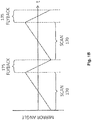
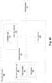
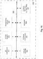
- FIG. 1A is a diagram of a scanning fluorescence imaging system 100 according to an example embodiment.
- the imaging system of FIG. 1A illuminates a portion of a substrate (e.g., such as an array chip) by scanning a line of light across the substrate while an image of the portion of the substrate is temporarily fixed on the sensor of a camera as the substrate is being moved under a microscope objective lens component.
- a substrate e.g., such as an array chip
- array chip 105 carries target nucleic acids such as, for example, DNA macromolecules.
- Positioning stage 110 moves array chip 105 with respect to objective lens component 115 in the y -direction, Positioning stage 110 is a high-precision, computer-controlled, air-bearing stage.
- Objective lens component 115 is an off-the-shelf objective.
- the objective lens component may be a custom-designed, multi-element optical component.
- water immersion may be used to increase the numerical aperture (NA) of the objective lens component.
- Tube lens component 120 is an element or group of elements that comprises one or more tube lenses that function as a second magnification objective.
- Camera 125 is a fast CMOS camera that preferably, but not exclusively, operates in full-frame mode and employs a sensor array characterized by low read noise, high resolution, and high imaging speed.
- scan mirror 130 is a lightweight mirror that is tilted by a servo rotation mechanism (not shown) in a range of angular motion.
- a servo rotation mechanism (not shown) in a range of angular motion.
- the area within the field of view 106 of objective lens component 115 is imaged onto camera 125 as image 107.
- a fixed area e.g., the field of view 106
- the rotation of scan mirror 130 (e.g., around an axis perpendicular to the plane of FIG. 1A ) has the effect of scanning an image in the y -direction shown in the figure. This result is obtained because tilt in the collimated section of imaging system 100, in which scan mirror 130 is placed, corresponds to lateral translation at the focal plane of camera 125.
- line generator 160 in the form of a line of illumination light 108.
- the line of light 108 is directed to and reflected by illumination mirror 140, which is placed in an optical path between line generator 160 and dichroic beam splitter 150.
- the line generator can emit light of various wavelengths that are compatible with various fluorophores that can be used in sequencing such as, for example, light of wavelength in a range from 400 nm to 800 nm.
- line generator 160 comprises light source 162 (e.g., such as one or more lasers or other source of illumination), one or more collimating lenses 164, and one or more negative cylindrical lenses 166.
- Collimating lens 164 transforms the light emitted from light source 162 into a parallel beam of light
- negative cylindrical lens 166 focuses the parallel beam into a line of light.
- the line of light generated in this manner is configured to have a length and/or width that correspond, after magnification, to the length and/or width of one or more rows of camera pixels.
- the length and width of the line of illumination light 108 is such that the corresponding line of exposure light 109 spans one or more rows of pixels in the sensor of camera 125.
- Illumination mirror 140 is a lightweight mirror that is tilted by a servo rotation mechanism (not shown) in a range of angular motion. As illumination mirror 140 tilts back and forth between an initial and an end position, the line of illumination light 108 generated by line generator 160 is reflected by the illumination mirror to dichroic beam splitter 150 and then to scan mirror 130, which in turn reflects it onto array chip 105 through objective lens component 115. Dichroic beam splitter 150 reflects at illumination wavelengths but transmits at fluorescence emission wavelengths; thus, beam splitter 150 reflects to scan mirror 130 the line of illumination light 108, and transmits to camera 125 the line of florescent exposure light 109. It is noted that in an imaging system that interrogates more than one type of fluorescent marker at a time, multiple illumination sources (e.g., such as multiple lasers each emitting a separate spectrum of light) and dichroic beam splitters may be used.
- illumination sources e.g., such as multiple lasers each emitting a separate spectrum of light
- Illumination mirror 140 is positioned in the optical path of the line of illumination light 108 in a manner that allows the angular motion of the illumination mirror to effectively move the line of light across array chip 105 in the same direction (e.g., y -direction) in which positioning stage 110 is moving array chip 105. Since the motion of illumination mirror 140 is synchronized and/or coordinated with the motions of scan mirror 130 and positioning stage 110, the motion of the illumination mirror causes the line of illumination light 108 to be effectively moved, or scanned, across the portion of array chip 105 that is within the field of view 106 of objective lens component 115.
- Rotating scan mirror 130 around an axis perpendicular to the plane of FIG. 1A has the effects of: (1) scanning the line of illumination light 108 onto array chip 105 in the y- direction (which is performed in coordination with the motion of illumination mirror 140), and (2) scanning an image 107 of a portion of array chip 105 also in the y -direction.
- camera 125 collects image 107 of the area within the field of view 106 of objective lens component 115. (It is noted that in some embodiments the camera may be operating in rolling readout mode, while in other embodiments it may be operating in full-frame mode).
- the image 107 collected by camera 125 spans multiple rows of camera pixels (such image is also referred to herein as a "two-dimensional" image). Since the line of light 108 illuminates only a small line of a portion of array chip 105 at a time, at any one time the corresponding line of exposure light 109 only exposes one or a few rows of pixels spanned by image 107 while keeping in the dark other row(s) of pixels spanned by the image.
- illumination mirror 140 scan mirror 130, and positioning stage 110 are coordinated and synchronized in such manner that the line of illumination light 108 is at least slightly ahead of those row(s) of pixels that are currently being read out from camera 125 by a computer logic (not shown) in imaging system 100.
- the line of exposure light 109 which is emitted by target nucleic acids on array chip 105 in response to excitation by the line of illumination light 108, is exposing row(s) of pixels in camera 125 that are (at least slightly) ahead of other row(s) of pixels that are currently being read out by the computer logic operating the camera.
- image data can be read out from the camera while other image data is being acquired by the camera sensor, thereby increasing the overall camera readout efficiency ⁇ .
- an imaging system may comprise one or more tilt plates, which are positioned in the optical path between the scan mirror and the camera, and which can be used to make small corrections to image placement on the sensor array of the camera - e.g., by using one tilt plate for corrections in the x -direction of the image and one tilt plate for corrections in the y -direction of the image.
- a tilt plate can be made of glass approximately 2.5 cm in diameter and 3.5 mm thick. The plate can be mounted on a servo rotation mechanism for quick and precise movements.
- ⁇ x t sin ⁇ ⁇ t n cos ⁇ sin ⁇ 1 ⁇ 1 n sin ⁇ 2
- t is the thickness of the plate
- n is its index of refraction
- ⁇ is the angle of incidence.
- information on image alignment with respect to the sensor array of the camera can be used to provide feedback signals that drive the x -direction tilt plate and/or the y -direction tilt plate.
- One source of such alignment information is the results of analyzing images acquired by the camera.
- Another source of alignment information in the y -direction can be obtained by monitoring the performance of the scan mirror by using one or more angle sensors that measure the tilt angle of the scan mirror precisely and quickly.
- image alignment information is sent to a computing device that executes the logic that controls the operation of the scan mirror, the chip positioning stage, the one or more tilt plates, and preferably (but not necessarily) the operation of the illumination source(s) and/or any illumination mirrors involved in illuminating the substrate being imaged.
- an imaging system can utilize the techniques for scanned illumination described herein without using a movable positioning stage and/or a movable scan mirror.
- an imaging system uses a movable illumination mirror to scan a line of illumination light across a stationary substrate and a camera operative to collect an image of a portion of the substrate.
- the camera operates in a mode (e.g., such as rolling readout mode or full-frame mode) that allows for exposing some row(s) of pixels while some other row(s) of pixels are being read out from the camera sensor. Since the substrate is stationary and is not moving during image acquisition, the imaging system does not need to employ a movable scan mirror to keep the image still on the camera.
- the motion of the illumination mirror and the operation of the computer logic, which reads out image data from the camera, are coordinated and synchronized in such manner that the line of exposure light (which is reflected from the substrate in response to the line of illumination light) is at least slightly ahead of those row(s) of pixels that are currently being read out from the camera by the computer logic.
- Such coordination and timing synchronization may depend on several factors that include, without limitation, the time necessary for sufficient exposure, the scan velocity of the line of illumination light across the substrate, and the like.
- the techniques for scanned illumination described herein can still be used to increase the overall readout efficiency ⁇ of the camera in some operational contexts, even though the imaging system does not employ a movable positional stage to image moving targets.
- embodiments e.g., such as the embodiment illustrated in FIG. 1A
- that use angularly movable illumination and scan mirrors in conjunction with linearly movable positioning stages are to be regarded in an illustrative rather than a restrictive sense.
- an imaging system uses a movable illumination mirror to scan a line of light across a substrate (e.g., such an array chip) while a movable scan mirror temporarily fixes an image of the portion of the substrate on a camera as a positioning stage is moving the substrate under a microscope objective lens component.
- the motion of the illumination mirror is coordinated with the motions of the scan mirror and the positioning stage in a manner that allows the motion of the illumination mirror to cause the line of illumination light to be effectively moved, or scanned, across the portion of the substrate that is within the field of view of the objective lens component.
- one or more computing devices in the imaging system execute computer logic that is configured and operative to synchronize the timing of the operations that read out image data from exposed row(s) of camera pixels with the motions of the illumination mirror, the scan mirror, and the positioning stage on which a target substrate is mounted.
- the positioning stage is moving the substrate mounted thereon while a computing device executes readout logic to read one or more rows of exposed pixels from the camera.
- the same and/or different computing device executes coordination logic that receives input data from the system elements that move the illumination mirror, the scan mirror, and the positioning stage, where examples of such input data include, without limitation, data specifying the current tilt angle of the illumination mirror, data specifying the current tilt angle of the scan mirror, and data specifying the position and velocity of the positioning stage.
- the coordination logic uses the input data to determine whether any corrections are necessary in the motions and the timings of the illumination mirror, the scan mirror, and the positioning stage, and if so sends any necessary correction terms to the system elements that facilitate such motions.
- the coordination logic synchronizes the operation of the illumination mirror, the scan mirror, the positioning stage, and the readout logic.
- the result of this synchronization is that the scan mirror keeps the image of the substrate (or portion thereof) still with respect to the camera while the illumination light is scanned across the substrate, while at the same time the readout logic extracts image data from row(s) of pixels that have already been exposed.
- the coordination logic ensures that the line of exposure light is ahead of the row(s) of pixels currently being read out, the illumination mirror and the scan mirror do not necessarily need to operate with tolerances as strict as the tolerances required for the scan mirror to keep the image still on the camera.
- the timing between readout logic, the illumination mirror, and the scan mirror may be synchronized within very strict tolerances in order to ensure that image data can be read out from the camera all, or almost all, of the time.
- the imaging systems need to lock the image acquired by the camera with a precision of 10-15 nm, which requires a high degree of synchronization between the respective timings of the illumination mirror, the scan mirror, the positioning stage, and the readout logic.
- the illumination mirror, the scan mirror, and the positioning stage are coordinated in a manner that allows the exposure of one or more row(s) of pixels in the camera while other row(s) are kept in the dark; as soon as the exposure is completed, a computing device executes the readout logic to read out the exposed row(s) of pixels while at the same time the imaging system continues to scan the line of light across the portion of the substrate to expose other row(s) of pixels in the camera.
- the overall readout efficiency ⁇ of the camera would be at maximum/optimum.
- the illumination is being scanned in the form of a line across the target substrate, charge is collected and integrated in a camera pixel only during the time interval in which the line of exposure light sweeps over that pixel; the rest of the time the pixel is in the dark and hence does not integrate any charge even though the pixel is ready to do so.
- the charges accumulated by a row of pixels can be read out by executing the readout logic, which reads the pixels row-by-row in a rolling fashion.
- the synchronization between the motions and timings of the illumination mirror and the scan mirror do not necessarily need to be within strict tolerance, but the illumination mirror needs to complete its cycle (e.g., from its initial position to its end position) within the "stable" time interval of the scan mirror (e.g., the time interval during which the scan mirror holds the image still with respect to the camera).
- any component that facilitates the scanning of the illumination e.g., such as a servo-controlled illumination mirror
- the implication of the fly-back time interval is that camera pixels should not be exposed during the scan mirror fly-back intervals but already-exposed pixels can be read out.
- FIG. 1B illustrates a diagram of scan mirror angle timing according to an example embodiment.
- the tilt angle of a scan mirror is plotted versus time, t .
- the mirror angle changes substantially linearly with time so that a camera can view a fixed area on a moving substrate.
- the scan mirror returns to its starting angle (e.g., in initial position) in preparation for a new scan.
- the starting angle e.g., in initial position
- image data may be read out from the camera at any time.
- image data is read out continuously from the camera for maximum data throughput (e.g., such as image conversion into digital data) since there is no reason to stop reading out data or slowing down throughput.
- the scan time interval, during which an image is collected by the camera must still be long enough to build up adequate signal-to-noise ratios as fluorescence imaging light levels are typically very weak.
- an acousto-optic modulator (AOM) switch (or other type of fast switch) may be used to turn on and off the line generator that generates the line of illumination light that is reflected onto the substrate being imaged.
- AOM acousto-optic modulator
- a suitable aperture can be placed in the optical path of the line of illumination light, where the line of illumination light is allowed to overscan but the aperture prevents the line of light from illuminating the substrate during the fly-back time intervals by blocking out the line of light outside of the field of view.
- a suitable shutter can be placed in the optical path of the line of illumination light, where the shutter is kept open during exposure intervals and is closed during the scan mirror fly-back time intervals.
- the techniques for scanned illumination described herein can avoid any reduction in camera readout efficiency that may be caused by the fly-back time intervals of scan mirrors that are used in imaging systems to scan moving targets
- FIG. 1C is a detail of object space areas within a field of view 106 of an objective lens component 115 according to the example embodiment of FIG. 1A .
- shaded rectangle 180 represents the area within field of view 106 that is imaged on the sensor array of a camera when the scan mirror of the imaging system is in a mid-range position.
- Rectangles 184 and 182 represent the area within field of view 106 that is imaged on the sensor array of the camera when the scan mirror is in its extreme initial and end positions, respectively.
- the objective lens component is focused on a substrate (e.g., such as an array chip) that is steadily moving in the y -direction and the scan mirror rotates from its initial position to its end position. If the velocity of the substrate is the same as the velocity of the field of view 106 that is imaged on the camera, then the image of the substrate portion corresponding to the field of view does not move with respect to the camera, thereby allowing sufficient exposure onto the camera sensor.
- a substrate e.g., such as an array chip
- the image is stationary with respect to the camera only during the time that the imaged object space area moves from the initial position indicated by rectangle 184 to the end position indicated by rectangle 182.
- the fly-back time interval can be configured to be only a small fraction of the scan mirror cycle, however, and consecutive imaged areas may be made contiguous or even overlap if necessary.
- the amount of time spent by the scan mirror on each imaged area is made commensurate with the camera's frame rate, thereby allowing sufficient time to expose an image of each object space area onto the camera while at the same time allowing image data to be read out from the camera for other object space areas that have already been imaged and are out of the field of view.
- the attachment sites of an array chip are divided into micron-to-millimeter sized fields.
- a typical field may be of a size in the ranges of 320-1600 ⁇ m by 320-1600 ⁇ m, 500-600 ⁇ m by 500-600 ⁇ m, or even 1.6 mm by 700 ⁇ m.
- a typical array chip may be divided into hundreds or thousands of fields that are arranged in a rectangular pattern of rows and columns.
- the rows and columns of fields may include track regions that are aligned substantially along a horizontal dimension and a vertical dimension, respectively.
- an imaging system images an array chip in a scanning fashion with scanned illumination (as described herein) while the positioning stage is moving the array chip along the y -direction in a plane and/or axis that is substantially normal to the optical axis of the objective lens component.
- the imaging system ceases imaging when the end of the column of field(s) being imaged is reached in order to allow the positioning stage to return the array chip and to position it for imaging of the next column of field(s).
- an imaging system images an array chip in a scanning fashion (as described herein) while the positioning stage is moving the array chip backward and forward in a serpentine fashion (e.g., along a -axis) in a plane that is substantially normal to the optical axis of the objective lens component.
- the imaging system images a column of field(s) while the positioning stage is moving the array chip in one direction and then images the next/adjacent column of field(s) while the positioning stage is moving/returning the array chip in the opposite direction; in other words, the imaging system images the array chip by effectively traversing the columns of fields in a continuous serpentine fashion.
- imaging systems use CMOS cameras that can operate in correlated double sampling mode to achieve low read noise. Further, the cameras in such systems may also operate in rolling readout mode to enhance throughput.
- FIG. 2 illustrates a diagram of example operations in rolling readout mode according to one embodiment.
- FIG. 2 illustrates a few representative rows of pixels (e.g., pixel 210) in the image sensor 205 of a digital camera.
- pixels e.g., pixel 210
- FIG. 2 illustrates a few representative rows of pixels (e.g., pixel 210) in the image sensor 205 of a digital camera.
- the image sensor of a camera may include anywhere between 250 and 10,000 rows of pixels and anywhere between 400 and 10,000 columns of pixels, for a total number of pixels in a range from 100,000 to 100 million pixels.
- rolling readout mode image data is read out from a camera sensor on a row-by-row basis. In other words, data from an entire row of pixels is read out simultaneously. As an example, image data from row 215 in FIG. 2 is read out at once. After that, data from an adjacent row of pixels is read out. According to the techniques described herein, rows are not readout randomly, but rather in a sweeping or "rolling" fashion up or down the sensor. For example, the two arrows in FIG. 2 suggest two possibilities: the next row of pixels read out after row 215 will be the adjacent row just above it, or the adjacent row just below it. Rolling readout mode can provide up to a factor of two increase in frame rate over global shutter or snapshot mode.
- the use of correlated double sampling to achieve low read noise means that image acquisition can begin immediately after readout. For example, pixels in the camera sensor can begin to accumulate light that contributes to image data immediately after data is read out. As long as no light falls on the camera sensor however, e.g., it is in the dark and is not exposed, then image noise does not build up.
- image noise does not build up.
- this new exposure mode is based on illuminating object space area (of whatever is to be imaged, e.g. such as a substrate) that corresponds to one, or just a few, rows of pixels in a camera sensor, where the illumination is scanned or "rolled" over the object space area.
- This exposure mode is referred to herein as "rolling exposure mode”.
- an imaging system operates in both rolling exposure mode (in which a line of light is scanned across the substrate being imaged) and rolling readout mode (in which rows of pixels are read out one after the other shortly after exposure). A period of darkness between exposure and read operations does not increase image noise.
- FIG. 3 illustrates expose and read regions of a camera being operated in both rolling exposure mode and rolling readout mode.
- FIG. 3 illustrates a few representative rows of pixels in camera sensor 305.
- Shaded row 315 is currently being exposed - that is, the pixels in row 315 are recording image data.
- Hatched row 320 is being read out - that is, the image data in row 320 is being converted into electronic bits suitable for transmission to, and manipulation by, a computing device.
- Rows such as row 325, between row 315 and row 320, are dark; these rows have accumulated and integrated light signal during previous exposure, but have not yet been read out.
- rows such as rows 330 and 335 are ready to collect image data (e.g., to accumulate and integrate light signal); with respect to the direction of the exposure and readout operations, such rows of pixels are located both behind the current readout row (e.g., such as row 320) and in front of the current exposure row (e.g., such as row 335).
- FIG. 3 shows only one row 315 being exposed, in practice a few (e.g., one to about 10 or so) rows of pixels may be exposed simultaneously.
- the rows of pixels being exposed correspond to the line of illumination light that is scanned across the object space area being imaged (e.g., such a portion of a substrate).
- the illuminated object space area corresponds to just one or a few rows of pixels in the camera sensor.
- the readout operation proceeds one row at a time in rolling readout mode as described above.
- the line of illumination light is scanned across an object space area corresponding to an exposure area of the camera sensor that includes row 315 (as indicated by the "EXPOSE” arrow).
- the readout area of the camera sensor (as indicated by the "DARK” arrow) includes row 320 and follows behind the exposure area.
- the exposure area and the readout area may "move" across the sensor at different speeds relative to each other.
- FIG. 4 illustrates a diagram of scan mirror angle, expose timing, and readout timing according to an example embodiment.
- the upper diagram 410 in FIG. 4 shows a scan mirror angle plotted versus time, t .
- the lower diagram 420 in FIG. 4 shows a plot of exposed/read row numbers versus time, t .
- Rows of pixels e.g., of a camera sensor
- Rows of pixels are numbered from “ 1 " to " N ", with the time sequence for row "x" expressly plotted out for illustration.
- Vertical slices (parallel to the dashed lines) of diagram 420 show which rows of pixels are being exposed or read during a particular time interval (e.g., such as a "SCAN" time interval or a "FLYBACK” time interval).
- Horizontal slices in diagram 420 e.g. as shown for row " x ", show exposure, dark, and readout periods for a particular row.
- the tilt angle of a scan mirror (which holds an image still with respect to a camera sensor) is a linear function of time during "SCAN” intervals; the angle resets to a starting position during "FLYBACK” intervals. Exposure and readout of camera sensor rows sweep from one side (row “ 1 ") of the sensor to the other (row “ N” ) and then back in the opposite direction (from row “ N “ back to row “ 1 "). While this may seem counterintuitive at first, it can be understood by remembering that the scan mirror “freezes" an image of a portion of a substrate (e.g., such as an array chip) on the camera sensor even though the substrate is moving in a direction that is normal to the objective lens component of the imaging system.
- a substrate e.g., such as an array chip
- the camera "sees" a still object that is illuminated by a moving line of light that covers an object space area corresponding to one (or a few) rows of camera pixels at a time.
- the readout operation is taking place in rolling readout mode a few rows behind the exposed row(s) of pixels.
- FIG. 4 illustrates that the time required to expose " N " rows of pixels is shorter than the time needed to read out the image data stored therein.
- the exposure operation takes up all of the available scan time, i.e. the time that an image is still with respect to the camera sensor.
- the readout operation can take place substantially continuously (with the only exception being the small delay that occurs before the beginning of exposure time for a first row in any given scan.)
- FIG. 4 illustrates the exposure period, the dark period, and the readout period for a single row.
- row " x '' as an example, exposure to illumination lasts for the "EXPOSE” time period 432.
- a "DARK" time period 434 follows the exposure period 432.
- the dark period 434 neither signal nor noise accumulates in the pixels of row " x ".
- the pixels of row “ x " are read out during the "READ” time period 436, which occurs after time period 434.
- the time period (e.g., the dark time period) between the exposure operation and the readout operation increases as the line of exposure light moves across the object because the exposure operation proceeds at a higher speed than the readout operation.
- the exposure period 432, the dark period 434, and the readout period 436 are repeated during the next scan mirror cycle as the sensor rows are exposed (for a new image) in the reverse direction (e.g., from row " N " back to row " 1 "), which can happen when the imaging system is configured to scan an object (e.g., such as substrate) by traversing the object in a serpentine fashion.
- an imaging system comprises a camera having a spilt-readout sensor.
- a split-readout sensor has at least two sections that can be exposed and read out independently of each other, where the exposure/readout operations in one section can be performed in parallel or in anti-parallel with respect the exposure/readout operations in the other section(s) of the sensor.
- each section of the split-readout sensor is illuminated with a separate line of light.
- Separate lines of light can be generated in various ways. For example, a separate line generator can be used to generate a separate line of light for each separate sensor section, where polarization can be used to direct the lines of light onto different portions of the same substrate.
- various optical components e.g., such as prisms, half-silvered mirror, etc.
- FIG. 5 illustrates a diagram of a split-readout camera sensor according to an example embodiment.
- a 2160 pixels by 2560 pixels sensor is split into "SECTION 1" and "SECTION 2".
- the number of pixels shown in the sensor of FIG. 5 corresponds to the SciMOS 2051 camera of Fairchild Imaging, Milpitas, California, and is used as an example only. Other cameras may use split-readout sensors of different dimensions.
- Each section of the sensor is read out independently of the other.
- Split-readout sensors lead to different ways of implementing the rolling exposure mode and the rolling readout mode described herein.
- FIGs. 6A and 6B illustrate a diagram of parallel operation of exposure and readout regions according to an example embodiment that uses a split-readout camera sensor.
- FIGs. 7A and 7B illustrate a diagram of anti-parallel operation of exposure and readout regions according to an example embodiment that uses a split-readout camera sensor.
- FIGs. 6A, 6B , 7A, and 7B illustrates a few representative rows of pixels in a camera sensor. For illustration purposes, only a few columns of pixels have been depicted in each of FIGs. 6A, 6B , 7A, and 7B ; however, it is noted that columns of pixels extend along the entire width of the depicted sensor --- that is, the sensor is a grid of rows and columns of pixels.
- the sensor illustrated in FIGs. 6A and 6B is similar to the sensor illustrated in FIG. 3 , except that the sensor of FIGs. 6A and 6B is a split-readout sensor having two sections. Pairs of exposure (marked “EXPOSE”) and readout (marked “READ”) regions, one pair for each section, move in the same direction in both sections of the sensor. For example, the pairs of exposure and readout regions move from top to bottom in both sections of the sensor in Fig. 6A and from bottom to top in both sections of the sensor in Fig. 6B . This mode of operation is referred to herein as "parallel" because the pairs of expose and readout regions of the sensor sections move in the same direction.
- the sensor illustrated in FIGs. 7A and 7B is similar to the split-readout sensor of FIGs. 6A and 6B .
- the pairs of exposure (marked “EXPOSE”) and readout (marked “READ”) regions in the sensor of FIGs. 7A and 7B move in opposite directions in the two sections of the sensor.
- FIG. 7A illustrates that the pair of exposure and readout regions move toward each other in the two sections of the sensor
- FIG. 7B illustrates that the pair of exposure and readout regions move away from each other in the two sections of the sensor.
- This mode of operation is referred to herein as "anti-parallel" because the pairs of expose and readout regions in the sensor sections move in opposite directions.
- each section of the split-readout sensors depicted in FIGs. 6A, 6B , 7A, and 7B may have an associated timing diagram similar to the timing diagram illustrated in FIG. 4 .
- timing diagrams for the lower sections of the sensor in FIGs. 7A and 7B may be similar to the timing diagram illustrated in FIG. 4 , but with row order " N "-to-" 1 " rather than " 1 "-to-” N " in order to account for the anti-parallel nature of the exposure/readout operations in the two sections of the sensor.
- the illumination, exposure, and readout techniques described in the present disclosure have been cast in terms of use with a movable scan mirror that has a dead fly-back time interval, persons skilled in the art would recognize that these techniques are more broadly applicable. For example, any imaging system that is limited to less than full duty cycle image acquisition may benefit from the techniques described herein. In another example, the techniques described herein may be implemented in an imaging system that uses a rotation polygon mirror for scanning instead of a movable scan mirror.
- the techniques for scanned illumination described herein are useful in imaging systems that use digital cameras operating in rolling exposure mode and rolling readout mode, that use correlated double sampling, and/or that are prevented from full duty cycle image acquisition.
- the techniques described herein may be implemented in an imaging system that uses one or more CMOS cameras for fluorescence-based DNA sequencing; in this embodiment, the techniques described herein contribute to overall sequencing throughput of about 100 human genome data equivalents per day.
- FIG. 8 illustrates an example method for imaging a substrate according to one embodiment.
- the method in FIG. 8 is described hereinafter as being performed by a sequencing machine that includes an imaging system; it is understood, however, that the steps of the method can be performed by various different types of devices and imaging systems.
- the method in FIG. 8 is not limited to being performed by any particular type of machine or device, and therefore the method description hereinafter is to be regarded in an illustrative rather than a restrictive sense.
- a camera collects an image of a portion of a substrate, where the image spans multiple rows of pixels in the camera.
- a positioning stage moves the substrate under an objective lens component in a plane that is normal to the optical axis of the objective lens component, where the substrate comprises a multitude of distinct features that are the targets of the imaging.
- the substrate comprises an array chip having target nucleic acids disposed thereon
- a sequencing machine includes an imaging system that in turn includes the camera, the positioning stage, and the objective lens component
- the camera may be a CMOS camera with a line rate in a range from 1,000 lines per second to 1,000,000 lines per second
- the positioning stage may move the substrate with a velocity in a range from 100 ⁇ m/second to 1,000 mm/second.
- a servo mechanism changes the angle of a scan mirror such that an image of the substrate portion, acquired by the objective lens component, is kept still with respect to the camera.
- a computing device that is part of, or coupled to, the sequencing machine executes logic that controls the servo mechanism in of the scan mirror coordination with the positioning stage.
- the logic receives feedback control information that represents the movement of the positioning stage and uses this information to adjust the input signal to the servo mechanism, which in turn changes the angle of the scan mirror thereby synchronizing the motion and/or the timing of the scan mirror with the motion and/or the timing of the positioning stage.
- step 804 while the camera is collecting the image of the portion of the substrate, the imaging system continuously and simultaneously performs (or causes to be performed) steps 806, 808, and 810. In some aspects, the camera collects a still image of the substrate portion while the substrate is being moved by a positioning stage.
- the imaging system and/or a computing device thereof scans (or causes the scan of) a line of light across the portion of the substrate being imaged, thereby continuously exposing one or more rows of pixels spanned by the image being collected while keeping in the darks other one or more rows spanned by the image.
- scanning the line of light across the substrate portion is performed in coordination with the motion of a scan mirror that keeps an image of the portion the moving substrate still with respect to the camera.
- a computing device coupled to, or part of, the imaging system executes logic that coordinates a servo mechanism that tilts an illumination mirror (which reflects the line of light from a line generator to the scan mirror) with a servo mechanism that tilts the scan mirror, thereby synchronizing the timing of the scan mirror with the timing of the illumination mirror to cause the scanning of the line of light onto the moving substrate.
- a computing device that is part of, or coupled to, the sequencing machine executes logic that continuously reads out rows of pixels that have already being exposed and are currently not acquiring any more light. For example, the computing device executes logic that reads out the rows of exposed pixels row-by-row in rolling readout mode.
- steps 806 and 808 are continuously synchronized in step 810, so that the readout operation of step 808 reads out any particular row of pixels just (or shortly) after this particular row of pixels has been exposed by the exposure operation of step 806.
- this synchronization of exposure and readout operations allows the camera to operate with readout efficiency of 55% to 90%, 90% to 95%, or even greater than 95%.
- sequencing of DNA samples may be performed by a sequencing system.
- FIGs. 9A and 9B illustrate example sequencing systems.
- FIGs. 9A and 9B are block diagrams of example sequencing systems 900 that are configured to perform DNA sequencing according to the example embodiments described herein.
- a sequencing system 900 can include multiple subsystems such as, for example, one or more sequencing machines such as sequencing machine 990, one or more computer systems such as computer system 997, and one or more data repositories such as data repository 995.
- the various subsystems of system 900 may be communicatively connected over one or more networks 993, which may include packet-switching or other types of network infrastructure devices (e.g., routers, switches, etc.) that are configured to facilitate information exchange between remote systems.
- network infrastructure devices e.g., routers, switches, etc.
- sequencing system 900 is a sequencing device in which the various subsystems (e.g., such as sequencing machine(s) 990, computer system(s) 997, and possibly data repository 995) are components that are communicatively and operatively coupled and integrated within the sequencing device.
- various subsystems e.g., such as sequencing machine(s) 990, computer system(s) 997, and possibly data repository 995
- data repository 995 and/or computer system(s) 997 of the embodiments illustrated in FIGs. 9A and 9B may be configured within a cloud computing environment.
- the storage devices comprising a data repository and/or the computing devices comprising a computer system may be allocated and instantiated for use as a utility and on-demand; thus, the cloud computing environment provides as services the infrastructure (e.g., physical and virtual machines, raw/block storage, firewalls, load-balancers, aggregators, networks, storage clusters, etc.), the platforms (e.g., a computing device and/or a solution stack that may include an operating system, a programming language execution environment, a database server, a web server, an application server, etc.), and the software (e.g., applications, application programming interfaces or APIs, etc. ) necessary to perform any storage-related and/or computing tasks.
- the infrastructure e.g., physical and virtual machines, raw/block storage, firewalls, load-balancers, aggregators, networks, storage
- the techniques described herein can be performed by various systems and devices that include some or all of the above subsystems and components (e.g., such as sequencing machines, computer systems, and data repositories) in various configurations and form factors; thus, the example embodiments and configurations illustrated in FIGs. 9A and 9B are to be regarded in an illustrative rather than a restrictive sense.
- a sequencing machine is configured and operative to receive one or more substrates that include target nucleic acids derived from fragments of a biological sample, and to perform sequencing on the target nucleic acids.
- Any suitable machine that can perform sequencing may be used, where such machine may use various sequencing techniques that include, without limitation, sequencing by hybridization, sequencing by ligation, sequencing by synthesis, single-molecule sequencing, and any other now-known or later-developed technique that is suitable for generating sequencing reads from DNA by using an imaging system as described herein.
- a sequencing machine can sequence the target nucleic acids and can generate sequencing reads that may or may not include gaps and that may or may not be mate-pair (e.g., paired-end) reads. As illustrated in FIGs.
- sequencing machine 990 sequences the target nucleic acids that are on substrate(s) 992 and obtains sequencing reads 994, which are transmitted for (temporary and/or persistent) storage to data repository 995 and/or for processing by one or more computer systems 997.
- sequencing machine 990 includes an imaging system 991 such as, for example, the imaging system illustrated in FIG. 1A .
- data repository 995 may be implemented on one or more storage devices (e.g., hard disk drives, optical disks, solid-state drives, etc.) that may be configured as an array of disks (e.g., such as a SCSI array), a storage cluster, or any other suitable storage organization.
- the storage device(s) of a data repository can be configured as internal/integral components of system 900 or as external components (e.g., such as external hard drives or disk arrays) attachable to system 900 (e.g., as illustrated in FIG.
- a data repository may be implemented on the storage devices as one or more file systems that store information as files, as one or more databases that store information in data records, and/or as any other suitable data storage organization.
- Computer system 997 may include one or more computing devices that comprise general purpose processors (e.g., Central Processing Units, or CPUs), memory, and computer logic 999 which, along with configuration data and/or operating system (OS) software, can perform some or all of the techniques and methods described herein.
- general purpose processors e.g., Central Processing Units, or CPUs
- OS operating system
- any of the methods involved in imaging e.g., such as image position correction, servo rotation control, scan mirror rotation and control, illumination mirror rotation and control, chip-positioning stage movement and synchronization, feedback control, image data readout, etc.
- any of the methods involved in imaging e.g., such as image position correction, servo rotation control, scan mirror rotation and control, illumination mirror rotation and control, chip-positioning stage movement and synchronization, feedback control, image data readout, etc.
- a computing device including a processor that can be configured to execute logic 999 for performing various steps of the methods.
- computer system 997 may be a single computing device.
- computer system 997 may comprise multiple computing devices that may be communicatively and/or operatively interconnected in a grid, a cluster, or in a cloud computing environment.
- Such multiple computing devices may be configured in different form factors such as computing nodes, blades, or any other suitable hardware configuration.
- computer system 997 in FIGs. 9A and 9B is to be regarded in an illustrative rather than a restrictive sense.
- FIG. 10 is a block diagram of an example computing device 1000 that can be configured to execute instructions for performing various methods involved in imaging as part of sequencing machine(s) and/or computer system(s).
- computing device 1000 comprises several components that are interconnected directly or indirectly via one or more system buses such as bus 1075.
- Such components may include, but are not limited to, keyboard 1078, persistent storage device(s) 1079 (e.g., such as fixed disks, solid-state disks, optical disks, and the like), and display adapter 1082 to which one or more display devices (e.g., such as LCD monitors, flat-panel monitors, plasma screens, and the like) can be coupled.
- display adapter 1082 to which one or more display devices (e.g., such as LCD monitors, flat-panel monitors, plasma screens, and the like) can be coupled.
- Peripherals and input/output (I/O) devices which couple to I/O controller 1071, can be connected to computing device 1000 by any number of means known in the art including, but not limited to, one or more serial ports, one or more parallel ports, and one or more universal serial buses (USBs).
- External interface(s) 1081 (which may include a network interface card and/or serial ports) can be used to connect computing device 1000 to a network (e.g., such as the Internet or a local area network (LAN)) and/or to other machines and devices.
- External interface(s) 1081 may also include a number of input interfaces that can receive information from various external devices.
- system bus 1075 allows one or more processors (e.g., CPUs) 1073 to communicate with each connected component and to execute (and control the execution of) instructions from system memory 1072 and/or from storage device(s) 1079, as well as the exchange of information between various components.
- processors e.g., CPUs
- System memory 1072 and/or storage device(s) 1079 may be embodied as one or more computer-readable non-transitory storage media that store the sequences of instructions executed by processors) 1073, as well as other data.
- Such computer-readable non-transitory storage media include, but is not limited to, random access memory (RAM), read-only memory (ROM), an electromagnetic medium (e.g., such as a hard disk drive, solid-state drive, thumb drive, floppy disk, etc.), an optical medium such as a compact disk (CD) or digital versatile disk (DVD), flash memory, and the like.
- RAM random access memory
- ROM read-only memory
- electromagnetic medium e.g., such as a hard disk drive, solid-state drive, thumb drive, floppy disk, etc.
- an optical medium such as a compact disk (CD) or digital versatile disk (DVD), flash memory, and the like.
- Various data values and other structured or unstructured information can be output from one component or subsystem to another component or subsystem, can be presented to a user via display adapter 1082 and a suitable display device, can be sent through external interface(s) 1081 over a network to a remote device or a remote data repository, or can be (temporarily and
- computing device 1000 can be implemented in the form of logic using hardware and/or computer software in a modular or integrated manner.
- logic When executed, such logic is adapted to perform the various methods involved in imaging (e.g., such as image position correction, servo rotation control, scan mirror rotation and control, illumination mirror rotation and control, chip-positioning stage movement and synchronization, feedback control, image data readout, etc.) as described herein.
- the imaging systems described herein may be used for a variety of biochemical analyses.
- One example of such analysis is sequence determination of target nucleic acids of unknown sequence.
- a variety of sequencing methodologies may be used to determine a sequence of the nucleic acid macromolecules using the imaging systems described herein, including, but not limited to: hybridization methods (e.g., as disclosed in US Patent Nos. 6,864,052 ; 6,309,824 ; and 6,401,267 ); sequencing-by-synthesis methods (e.g., as disclosed in US Patent Nos. 6,210,891 ; 6,828,100 , 6,833,246 ; 6,911,345 ; Margulies, et al.
- fluorescent signals emitted from target nucleic acids disposed on a substrate are recorded by imaging them onto sensor arrays of a camera in accordance with the techniques described herein.
- a substrate e.g., such as an array chip
- each pixel in a sensor array records the results of a separate fluorescence experiment, while in other imaging systems more than one pixel is used per experiment.
- biochemical substrates allow millions of biochemical experiments to be performed in parallel. This ability accrues from the development of techniques to perform each experiment in a very small volume and to pack the experiments very close together.
- a large number of attachment sites may be configured on an array chip in regular or random patterns, where the number of attachment sites may preferably be in a range from 5 billion to 50 billion, and more preferably in a range from 10 billion to 15 billion, and more generally in any sub-ranges in-between; in embodiments that use regular patterns, the pitch between the centers of any two adjacent attachment sites may be in a range from 250 nm to 1.5 ⁇ m.
- various embodiments preferably provide single-molecule occupancy at 60% to 95% of the attachment sites; further, the yield (e.g., the average number of macromolecules or target nucleic acids that emit a signal at any given imagining run) in various embodiments may preferably be in a range from 35% to 65% of all attachment sites that hold macromolecules or target nucleic acids.
- DNA sequencing includes chemical processing of DNA samples, physical analysis of the processed samples to obtain raw sequence fragments, and assembly of the sequence fragments into complete genomes using computational algorithms.
- multiple chemical processing and physical analysis cycles may be used to build up raw sequence data before computational work begins.
- fluorescence imaging is used to identify DNA bases - A, C, G, or T - by designing biochemical reactions such that a different colored dye (for example, red, green, blue, or yellow) corresponds to each one. Images of such DNA experiments for each color may then be taken through an objective lens component (e.g., such as a microscope objective). The colors observed indicate the DNA bases at a particular chemical processing step. Extracting data from such images thus depends on recording the color of fluorescence emitted by many millions or even billions of biochemical experiments that are conducted on a substrate (e.g., such as a chip).
- a substrate e.g., such as a chip
- the imaging systems described herein may be used for DNA sequencing of whole human genomes such as, for example, genomes of human individuals.
- Commercial viability of human genome sequencing depends in part on the ability to sequence DNA rapidly and accurately.
- the imaging systems described herein satisfy these criteria because they support processing of large numbers of parallel DN A experiments (e.g., that are being disposed at high density on an array chip), and can facilitate rapid and accurate genomic data acquisition.
- cPAL sequencing is the high-accuracy, combinatorial probe-anchor ligation (cPAL) sequencing that is commercially developed by Complete Genomics, Inc. of Mountain View, California.
- the cPAL sequencing technique relies on independently assaying each base from self-assembling DNA nanoballs ("DNBs") that are loaded into patterned arrays on array chips.
- DNBs DNA nanoballs
- the first step in cPAL sequencing is loading a biochemical array chip with a random assortment of DNBs.
- a DNB is a concatemer that contains multiple copies, linked in a series, of the same sequence of adapters and DNA fragments that represent target nucleic acid(s); the production of such concatemers is described, for example, in U.S. Patent Application Serial No.
- a set of DNBs contains DNA fragments that can collectively span an entire human genome, but when the DNBs are first attached to the attachment sites on an array chip there is no control over where any particular DNB goes. On the other hand, once the DNBs have attached to the attachment sites, they stay there for all subsequent liquid processing steps and don't move from one site to another. In subsequent processing steps various reagents and buffers are washed over the DNBs on the array chip, and fluorescent signals from the DNBs are recorded with a fluorescence imaging system.
- the cPAL sequencing technique comprises cycling of the following steps.
- an anchor is hybridized to a first adaptor in the DNBs (typically immediately at the 5' or 3' end of one of the adaptors).
- Enzymatic ligation reactions are then performed with the anchor to a fully degenerate probe population of, e.g., 8-mer probes, that are labeled, e.g., with fluorescent dyes.
- Probes may have a length, e.g., about 6-20 bases, or, preferably, about 7-12 bases.
- the population of 8-mer probes that is used is structured such that the identity of one or more of its positions is correlated with the identity of the fluorophore attached to that 8-mer probe.
- a set of fluorophore-labeled probes for identifying a base immediately adjacent to an adaptor may have the following structure: 3'-F1-NNNNNNAp, 3'-F2-NNNNNNGp, 3'-F3-NNNNNNCp, and 3'-F4-NNNNNNTp (where "p" is a phosphate available for ligation).
- a set of fluorophore-labeled 7-mer probes for identifying a base that is three bases into a target nucleic acid from an adaptor may have the following structure: 3'-F1-NNNNANNp, 3'-F2-NNNNGNNp, 3'-F3-NNNNCNNp, and 3'-F4-NNNNTNNp. (It is to be understood that these are not genome sequences to be catalogued, but are merely examples of structure for illustrative purposes.) To the extent that the ligase discriminates for complementarity at that queried position, the fluorescent signal provides the identity of that base.
- the anchor 8-mer probe complexes are stripped and a new cycle is begun.
- T4 DNA ligase accurate sequence information can be obtained as far as six bases or more from the ligation junction, allowing access to at least 12 base-pairs (bp) per adaptor (six bases from both the 5' and 3' ends), for a total of 48 bp per 4-adaptor DNB, 60 bp per 5-adaptor DNB, and so on.
- the 8-mer probes are structured differently. Specifically, a single position within each 8-mer probe is correlated with the identity of the fluorophore with which it is labeled. Additionally, the fluorophore molecule is attached to the opposite end of the 8-mer probe relative to the end targeted to the ligation junction. For example, an anchor may be hybridized such that its 3' end is adjacent to the target nucleic acid.
- a population of degenerate 8-mer probes may be used, where the probes correlate with the fifth nucleic acid from the 5' end of the 8-mer probe, which is the end of the 8-mer probe that will ligate to the anchor.
- the 8-mer probes are individually labeled with one of four fluorophores, where a fluorophore of Cy5 is correlated with A, Cy3 is correlated with G, Texas Red is correlated with C, and FITC is correlated with T. (although this example describes use of four fluorophores to query a single base per cycle, it should be recognized that eight or sixteen fluorophores or more may be used per cycle, increasing the number of bases that can be identified during any one cycle.)
- cPAL or other sequencing-by-ligation approaches may be selected depending on various factors such as the volume of sequencing desired, the type of labels employed, the number of different adaptors used within each library construct, the number of bases being queried per cycle, how the DNBs are attached to the surface of the array, the desired speed of sequencing operations, signal detection approaches, and the like.
- the degenerate (e.g., 8-mer) probes can be labeled in a variety of ways, including the direct or indirect attachment of radioactive moieties, fluorescent moieties, colorimetric moieties, chemiluminescent moieties, and the like.
- Many comprehensive reviews of methodologies for labeling DNA and constructing DNA adaptors provide guidance applicable to constructing oligonucleotide probes of the present invention. Such reviews include Kricka (2002), Ann. Clin. Biochem., 39: 114-129 , and Haugland (2006); Handbook of Fluorescent Probes and Research Chemicals, 10th Ed. (Invitrogen/Molecular Probes, Inc., Eugene ); Keller and Manak (1993), DNA Probes, 2nd Ed. (Stockton Press, New York, 1993 ); and Eckstein (1991), Ed., Oligonucleotides and Analogues: A Practical Approach (IRL Press, Oxford ); and the like.
- one or more fluorescent dyes are used as labels for the oligonucleotide probes. Labeling can also be carried out with quantum dots, as disclosed in the following U.S. patents and U.S. patent publications: 6,322,901 ; 6,576,291 ; 6,423,551 ; 6,251,303 ; 6,319,426 ; 6,426,513 ; 6,444,143 ; 5,990,479 ; 6,207,392 ; 2002/0045045 ; 2003/0017264 ; and the like.
- fluorescent nucleotide analogues readily incorporated into the degenerate probes include, for example, Cascade Blue, Cascade Yellow, Dansyl, lissamine rhodamine B, Marina Blue, Oregon Green 488, Oregon Green 514, Pacific Blue, rhodamine 6G, rhodamine green, rhodamine red, tetramethylrhodamine, Texas Red, the Cy fluorophores, the Alexa Fluor® fluorophores, the BODIPY® fluorophores and the like. FRET tandem fluorophores may also be used.
- suitable labels for detection oligonucleotides may include fluorescein (FAM), digoxigenin, dinitrophenol (DNP), dansyl, biotin, bromodeoxyuridine (BrdU), hexahistidine (6xHis), phosphor-amino acids (e.g. P-tyr, P-ser, P-thr) or any other suitable label.
- Image acquisition of such sequencing cycles can be performed by sequencing systems that include the imaging systems described herein.
- Data extraction may be performed by computing device(s) that execute(s) a series of binaries compiled from source code written in a programming language (e.g., such as C/C++), and base-calling and read-mapping may be performed by a series of Matlab and/or Perl scripts.
- a hybridization reaction for each base in a target nucleic acid to be queried (e.g., for 12 bases, reading 6 bases in from both the 5' and 3' ends of each target nucleic acid portion of each DNB), a hybridization reaction, a ligation reaction, imaging, and a primer stripping reaction is performed.
- each field of view (“frame") is imaged with four different wavelengths corresponding to the four fluorescent, e.g., 8-mers used. All images from each cycle are saved in a cycle directory, where the number of images is 4x the number of frames (for example, if a four-fluorophore technique is employed). Cycle image data may then be saved into a directory structure organized for downstream processing.
- Data extraction typically requires two types of image data: bright field images to demarcate the positions of all DNBs in the array; and sets of fluorescence images acquired during each sequencing cycle.
- a computing device executes data extraction software to identify all objects with the brightfield images, then for each such object, to compute an average fluorescence value for each sequencing cycle. For any given cycle, there are four data-points, corresponding to the four images taken at different wavelengths to query whether that base is an A, G, C, or T. These raw base-calls are consolidated, yielding a (possibly discontinuous) sequencing read for each DNB. These sequencing reads may then be matched against a reference genome by using various techniques and algorithms that can be performed on one or more computer systems that include one or more computing devices.
- reagents, buffers, and other fluids that are prepared by conventional techniques involving organic chemistry, polymer technology, molecular biology (including recombinant techniques), cell biology, and biochemistry, which are within the skill of those who practice in the art.
- Such conventional techniques may include, without limitation, polymer array synthesis, hybridization and ligation of polynucleotides, and detection of hybridization using a label.
- Specific illustrations of suitable techniques can be had by reference to the examples herein.
- other equivalent procedures can, of course, also be used. Such procedures can be found in standard laboratory manuals such as Green, et al., Eds. (1999), Genome Analysis: A Laboratory Manual Series (Vols.
- Adaptor refers to an engineered construct comprising "adaptor elements” where one or more adaptors may be interspersed within target nucleic acid in a library construct.
- the adaptor elements or features included in any adaptor may vary widely depending on the use of the adaptors, but typically include sites for restriction endonuclease recognition and/or cutting, sites for primer binding (e.g., for amplifying the library constructs) or anchor primer binding (e.g., for sequencing the target nucleic acids in the library constructs), nickase sites, and the like.
- adaptors are engineered so as to comprise one or more of the following: 1) a length of about 20 to about 250 nucleotides, or about 40 to about 100 oligonucleotides, or less than about 60 nucleotides, or less than about 50 nucleotides; 2) features so as to be ligated to the target nucleic acid as two "arms"; 3) different and distinct anchor binding sites at the 5' and the 3' ends of the adaptor for use in sequencing of adjacent target nucleic acid(s); and 4) one or more restriction sites.
- Amplicon refers to the product of a polynucleotide amplification reaction.
- an amplicon may be a population of polynucleotides that are replicated from one or more starting sequences. Amplicons may be produced by a variety of amplification reactions, including but not limited to polymerase chain reactions (PCRs), linear polymerase reactions, nucleic acid sequence-based amplification, circle dependent amplification and like reactions (see, e.g., US Pat. Nos. 4,683,195 ; 4,965,188 ; 4,683,202 ; 4,800,159 ; 5,210,015 ; 6,174,670 ; 5,399,491 ; 6,287,824 and 5,854,033 ; and US Pub. No. 2006/0024711 ).
- CDA cle dependent amplification
- the primers used may be of a random sequence (e.g., random hexamers) or may have a specific sequence to select for amplification of a desired product.
- CDA results in a set of concatemeric double-stranded fragments.
- CDR cle dependent replication
- the primer(s) used may be of a random sequence (e.g., one or more random hexamers) or may have a specific sequence to select for amplification of a desired product. Without further modification of the end product, CDR often results in the creation of a linear construct having multiple copies of a strand of the circular template in tandem, e.g., such as a linear concatemer of multiple copies of a strand of the template.
- Complementary or “substantially complementary” refers to the hybridization or base pairing or the formation of a duplex between nucleotides or nucleic acids, such as, for instance, between the two strands of a double-stranded DNA molecule or between an oligonucleotide primer and a primer binding site on a single-stranded nucleic acid.
- Complementary nucleotides are, generally, A and T (or A and U), or C and G.
- Two single-stranded RNA or DNA molecules are said to be substantially complementary when the nucleotides of one strand, optimally aligned and compared and with appropriate nucleotide insertions or deletions, pair with at least about 80% of the other strand, usually at least about 90% to about 95%, and even about 98% to about 100%.
- Duplex means at least two oligonucleotides or polynucleotides that are fully or partially complementary and which undergo Watson-Crick type base pairing among all or most of their nucleotides so that a stable complex is formed.
- annealing and “hybridization” are used interchangeably to mean formation of a stable duplex.
- Perfectly matched in reference to a duplex means that the poly- or oligonucleotide strands making up the duplex form a double-stranded structure with one another such that every nucleotide in each strand undergoes Watson-Crick base pairing with a nucleotide in the other strand.
- a "mismatch” in a duplex between two oligonucleotides or polynucleotides means that a pair of nucleotides in the duplex fails to undergo Watson-Crick base pairing.
- Fluorophore refers to a molecule comprising or consisting of a functional group that absorbs energy within a specific absorption spectrum and re-emits energy at a different (but equally specific) emission spectrum.
- Preferred fluorophores for use as markers include, but are not limited to, fluorescein, cascade blue, hexachloro-fluorescein, tetrachloro-fluorescein, TAMRA, ROX, FAM, Cy3, Cy3.5, Cy5, Cy5.5, 4,4-difluoro-5,7-diphenyl-4-bora-3a,4a-diaza-s-indacene-3-propionic acid, 4,4-difluoro-5,p-methoxyphenyl-4-bora-3a,4a-diaza-s-indacene-3-propionic acid, 4,4-difluoro-5-styryl-4-bora-3a,4-adiaz-a-S-indacene-
- Hybridization refers to the process in which two single-stranded polynucleotides bind non-covalently to form a stable double-stranded polynucleotide.
- the resulting (and usually) double-stranded polynucleotide is a "hybrid” or “duplex.”
- “Hybridization conditions” will typically include salt concentrations of less than about 1M, more typically less than about 500 mM and may be less than about 200 mM.
- a “hybridization buffer” is a buffered salt solution such as 5% SSPE, or other such buffers known in the art.
- Hybridization temperatures can be as low as 5°C, but are typically greater than 22°C, and more typically greater than about 30°C, and typically in excess of 37°C.
- Hybridizations are usually performed under stringent conditions, e.g., conditions under which a probe will hybridize to its target subsequence but will not hybridize to the other, uncomplimentary sequences.
- Stringent conditions are sequence-dependent and are different in different circumstances. For example, longer fragments may require higher hybridization temperatures for specific hybridization than short fragments.
- the combination of parameters is more important than the absolute measure of any one parameter alone.
- Generally stringent conditions are selected to be about 5°C lower than the T m for the specific sequence at a defined ionic strength and pH.
- Exemplary stringent conditions include a salt concentration of at least 0.01M to no more than 1M sodium ion concentration (or other salt) at a pH of about 7.0 to about 8.3 and a temperature of at least 25°C.
- 5xSSPE 750 mM NaCl, 50 mM sodium phosphate, 5 mM EDTA at pH 7.4
- a temperature of 30°C are suitable for allele-specific probe hybridizations.
- Ligation refers to the process of forming a covalent bond or linkage between the termini of two or more nucleic acids, e.g., oligonucleotides and/or polynucleotides, in a template-driven reaction.
- the nature of the bond or linkage may vary widely and the ligation may be carried out enzymatically or chemically.
- ligations are usually carried out enzymatically to form a phosphodiester linkage between a 5' carbon terminal nucleotide of one oligonucleotide with a 3' carbon of another nucleotide.
- Template driven ligation reactions are described in the following references: US Pat. Nos. 4,883,750 ; 5,476,930 ; 5,593,826 ; and 5,871,921 .
- nucleotide refer generally to at least two nucleotides that are covalently linked together.
- a nucleotide is composed of a nucleobase (or just “base”), a five-carbon sugar (e.g., such as a ribose or 2'-deoxyribose), and one to three phosphate groups that form the backbone of the nucleotide.
- the base e.g., one of the four main nucleotide bases of C, G, A, T, and the base U found in RNA
- the sugar comprise a nucleoside.
- a polynucleotide generally contains phosphodiester bonds, although in some cases nucleic acid analogs may be included that have alternative backbones such as, for example: phosphoramidite, phosphorodithioate, or methylphophoroamidite linkages; and peptide nucleic acid backbones and linkages.
- nucleic acid analogs include those with bicyclic structures including locked nucleic acids, positive backbones, non-ionic backbones, and non-ribose backbones.
- Primer refers to an oligonucleotide, either natural or synthetic, which is capable, upon forming a duplex with a polynucleotide template, of acting as a point of initiation of nucleic acid synthesis and being extended from one of its ends along the template so that an extended duplex is formed.
- the sequence of nucleotides added during the extension process is determined by the sequence of the template polynucleotide. Primers usually are extended by a DNA polymerase.
- T m is a term commonly defined as the temperature at which half of the population of double-stranded nucleic acid molecules becomes dissociated into single strands.
Landscapes
- Engineering & Computer Science (AREA)
- Multimedia (AREA)
- Physics & Mathematics (AREA)
- Signal Processing (AREA)
- General Physics & Mathematics (AREA)
- Chemical & Material Sciences (AREA)
- Analytical Chemistry (AREA)
- Health & Medical Sciences (AREA)
- Optics & Photonics (AREA)
- Theoretical Computer Science (AREA)
- General Health & Medical Sciences (AREA)
- Nuclear Medicine, Radiotherapy & Molecular Imaging (AREA)
- Life Sciences & Earth Sciences (AREA)
- Biochemistry (AREA)
- Computer Vision & Pattern Recognition (AREA)
- Immunology (AREA)
- Pathology (AREA)
- Investigating, Analyzing Materials By Fluorescence Or Luminescence (AREA)
- Microscoopes, Condenser (AREA)
- Studio Devices (AREA)
- Mechanical Optical Scanning Systems (AREA)
- Image Input (AREA)
Claims (21)
- Verfahren zum Betreiben eines Abbildungssystems (100), wobei das Verfahren umfasst:Sammeln eines zwei-dimensionalen Bildes eines Teils eines Substrats (105) auf einem Positioniertisch (110) über eine Digitalkamera (125) in dem Abbildungssystem (100) durch Bewegen des Positioniertisches (110) in einem ersten Verfahrweg unter einer Objektivlinsenkomponente (115) des Abbildungssystems (100), der senkrecht zur optischen Achse der Objektivlinsenkomponente (115) verläuft, wobei das Bild mehrere Reihen von Pixeln eines Sensorelements in der Kamera (125) überspannt;während die Kamera (125) das Bild des Teils des Substrats (105) sammelt, Durchführen von Schritten, die umfassen:Ändern eines Winkels eines Scanspiegels (130), der im optischen Pfad zwischen der Objektivlinsenkomponente (115) und der Kamera (125) angeordnet ist, so dass das Bild des Teils des Substrats (105) in Bezug auf die Kamera (125) still gehalten wird, während sich der Positioniertisch bewegt;Scannen einer von einem Liniengenerator (160) erzeugten Lichtlinie über den Teil des Substrats (105) durch Ändern eines Winkels eines Beleuchtungsspiegels (140), wodurch erste ein oder mehrere Reihen von Pixeln, die von dem Bild überspannt werden, belichtet werden, während zweite ein oder mehrere Reihen von Pixeln, die von dem Bild überspannt werden, im Dunkeln gehalten werden; undAuslesen der ersten ein oder mehreren Reihen von Pixeln, während das Scannen der Lichtlinie über den Teil des Substrats (105) fortgesetzt wird, wodurch die zweiten ein oder mehreren Reihen von Pixeln belichtet werden.
- Verfahren nach Anspruch 1, wobei das Ändern des Winkels des Scanspiegels (130) in Koordination mit dem Scannen der Lichtlinie über den Teil des Substrats (105) durchgeführt wird.
- Verfahren nach Anspruch 1, wobei:das Ändern des Winkels des Scanspiegels (130) ein erstes Zeitintervall umfasst, während dessen die Lichtlinie über den Teil des Substrats (105) gescannt wird, und ein zweites Zeitintervall, während dessen der Scanspiegel (130) in eine Ausgangsposition zurückgeführt wird; unddas Verfahren des Weiteren das Beenden des Scannens der Lichtlinie über den Teil des Substrats (105) während des zweiten Zeitintervalls umfasst.
- Verfahren nach Anspruch 3, wobei das erste Zeitintervall größer ist als das zweite Zeitintervall.
- Verfahren nach Anspruch 1, wobei das Auslesen der ersten ein oder mehreren Reihen von Pixeln durchgeführt wird, während das Substrat (105) in einer Richtung bewegt wird, die senkrecht zur optischen Achse der Objektivlinsenkomponente (115) verläuft.
- Verfahren nach Anspruch 1, wobei das Ändern des Winkels des Beleuchtungsspiegels (140) durch einen Servomechanismus bewirkt wird, der zum Kippen des Beleuchtungsspiegels (140) ausgebildet ist.
- Verfahren nach Anspruch 1, des Weiteren umfassend das im Dunkeln halten der ersten ein oder mehreren Reihen von Pixeln zwischen den Schritten des Belichtens der ersten ein oder mehreren Reihen von Pixeln und des Auslesens der ersten ein oder mehreren Reihen von Pixeln.
- Verfahren nach Anspruch 1, wobei die Kamera (125) einen Split-Readout-Sensor mit mindestens einem ersten Abschnitt und einem zweiten Abschnitt umfasst, und die Schritte des Scannens der Lichtlinie und des Auslesens unabhängig in jedem Abschnitt des Split-Readout-Sensors durchgeführt werden.
- Verfahren nach Anspruch 8, wobei die Schritte des Scannens und des Auslesens in dem ersten Abschnitt parallel zu den Schritten des Scannens und des Auslesens in dem zweiten Abschnitt durchgeführt werden.
- Verfahren nach Anspruch 8, bei dem die Schritte des Scannens und des Auslesens in dem ersten Abschnitt antiparallel zu den Schritten des Scannens und des Auslesens in dem zweiten Abschnitt durchgeführt werden.
- Verfahren nach Anspruch 1, des Weiteren umfassend:
während die Kamera (125) das Bild des Teils des Substrats (105) sammelt, Auslesen der zweiten ein oder mehreren Reihen von Pixeln, während das Scannen der Lichtlinie über das Substrat (105) fortgesetzt wird, wodurch dritte ein oder mehrere Reihen von Pixeln belichtet werden, die von dem Bild überspannt werden, wobei die dritten ein oder mehreren Reihen von Pixeln sich von der zweiten ein oder mehreren Reihen von Pixeln unterscheiden. - Verfahren nach Anspruch 1, wobei die Kamera (125) entweder eine CMOS-Kamera oder eine Nicht-CMOS-Kamera ist, die im Vollbildmodus arbeitet.
- Verfahren nach Anspruch 11, wobei die dritten ein oder mehreren Reihen von Pixeln sich von der ersten ein oder mehreren Reihen von Pixeln unterscheiden.
- Verfahren nach Anspruch 1, des Weiteren umfassend das Zurückfahren des Scanspiegels, während das Auslesen aus dem Sensorelement fortgesetzt wird.
- Abbildungssystem (100), umfassend:eine Objektivlinsenkomponente (115);einen Liniengenerator (160), der so ausgebildet ist, dass er eine Lichtlinie erzeugt, die über einen Teil eines Substrats (105) gescannt wird;einen Positioniertisch (110), der so ausgebildet ist, dass er das Substrat (105) in einem ersten Verfahrweg bewegt, der im Wesentlichen senkrecht zu einer optischen Achse der Objektivlinsenkomponente (115) verläuft;eine Digitalkamera (125), die so ausgebildet ist, dass sie ein zwei-dimensionales Bild des Teils des Substrats (105) durch die Objektivlinsenkomponente (115) erfasst;einen Scanspiegel (130), der so ausgebildet ist, dass er sich in Koordination mit dem Positioniertisch (110) bewegt, während die Lichtlinie über den Teil des Substrats (105) gescannt wird und das Substrat (105) in einer kontinuierlichen Bewegung auf dem ersten Verfahrweg bewegt wird, um das Bild in Bezug auf die Kamera (125) ruhig zu halten, während das Bild von der Kamera (125) erfasst wird; undeinen Beleuchtungsspiegel (140) und eine Computerlogik, wobei das Bild mehrere Reihen von Pixeln in der Kamera (125) überspannt, und wobei, während die Kamera (125) das Bild des Teils des Substrats (105) erfasst: der Beleuchtungsspiegel (140) so ausgebildet und betreibbar ist, dass er die Lichtlinie über den Teil des Substrats (105) scannt, um erste ein oder mehrere Reihen von Pixeln, die von dem Bild überspannt werden, zu belichten, während zweite ein oder mehrere Reihen von Pixeln, die von dem Bild überspannt werden, im Dunkeln gehalten werden; und die Computerlogik so ausgebildet und betreibbar ist, dass sie die ersten ein oder mehreren Reihen von Pixeln ausliest, während der Beleuchtungsspiegel (140) fortfährt, die Lichtlinie über den Teil des Substrats (105) zu scannen, um die zweiten ein oder mehreren Reihen von Pixeln zu belichten.
- Abbildungssystem (100) nach Anspruch 15, des Weiteren umfassend einen Beleuchtungsspiegel (140), der so ausgebildet ist, dass er die Lichtlinie von dem Liniengenerator auf den Teil des Substrats (105) scannt, wobei der Scanspiegel (130) so ausgebildet ist, dass er sich in Koordination mit dem Beleuchtungsspiegel (140) bewegt, während die Lichtlinie über den Teil des Substrats (105) gescannt wird und das Substrat (105) in der bestimmten Richtung bewegt wird.
- Abbildungssystem (100) nach Anspruch 16, des Weiteren umfassend:einen ersten Servomechanismus, der so ausgebildet ist, dass er einen Winkel des Beleuchtungsspiegels (140) ändert, um die Lichtlinie über den Teil des Substrats (105) zu scannen; undeinen zweiten Servomechanismus, der so ausgebildet ist, dass er einen Winkel des Scanspiegels (130) in Koordination mit Änderungen des Winkels des Beleuchtungsspiegels (140) ändert.
- Abbildungssystem (100) nach Anspruch 17, wobei:der zweite Servomechanismus so ausgebildet ist, dass er den Winkel des Scanspiegels (130) während eines ersten Zeitintervalls ändert, in dem die Lichtlinie über den Teil des Substrats (105) gescannt wird;der zweite Servomechanismus so ausgebildet ist, dass er den Scanspiegel (130) während eines zweiten Zeitintervalls, in dem die Lichtlinie nicht über den Teil des Substrats (105) gescannt wird, in eine Ausgangsposition zurückführt, wobei das zweite Zeitintervall kürzer ist als das erste Zeitintervall.
- Abbildungssystem (100) nach Anspruch 15, des Weiteren umfassend einen dichroitischen Spiegel, der zumindest ausgebildet ist, um: (a) die Lichtlinie von dem Beleuchtungsspiegel (140) auf den Scanspiegel (130) zu reflektieren, um den Teil des Substrats (105) zu beleuchten; und (b) Licht, das von der Objektivlinsenkomponente (115) erfasst und von dem Scanspiegel (130) reflektiert wird, an die Kamera (125) weiterzuleiten.
- Abbildungssystem (100) nach Anspruch 15, wobei die Kamera (125) einen Split-Readout-Sensor mit mindestens zwei Abschnitten umfasst, die unabhängig voneinander belichtet und ausgelesen werden können.
- Abbildungssystem (100) nach Anspruch 15, wobei das System so ausgebildet ist, dass es den Scanspiegel zurückfährt, während es weiterhin das Sensorelement ausliest.
Applications Claiming Priority (4)
| Application Number | Priority Date | Filing Date | Title |
|---|---|---|---|
| US201261656701P | 2012-06-07 | 2012-06-07 | |
| US201261656774P | 2012-06-07 | 2012-06-07 | |
| US13/908,964 US9488823B2 (en) | 2012-06-07 | 2013-06-03 | Techniques for scanned illumination |
| PCT/US2013/044250 WO2013184758A2 (en) | 2012-06-07 | 2013-06-05 | Techniques for scanned illumination |
Publications (3)
| Publication Number | Publication Date |
|---|---|
| EP2859396A2 EP2859396A2 (de) | 2015-04-15 |
| EP2859396A4 EP2859396A4 (de) | 2016-03-30 |
| EP2859396B1 true EP2859396B1 (de) | 2021-07-21 |
Family
ID=49712827
Family Applications (1)
| Application Number | Title | Priority Date | Filing Date |
|---|---|---|---|
| EP13801133.3A Active EP2859396B1 (de) | 2012-06-07 | 2013-06-05 | Verfahren für abgetastete beleuchtung |
Country Status (6)
| Country | Link |
|---|---|
| US (2) | US9488823B2 (de) |
| EP (1) | EP2859396B1 (de) |
| JP (1) | JP6317340B2 (de) |
| CN (1) | CN104487884B (de) |
| HK (1) | HK1203634A1 (de) |
| WO (1) | WO2013184758A2 (de) |
Families Citing this family (39)
| Publication number | Priority date | Publication date | Assignee | Title |
|---|---|---|---|---|
| CN101910399B (zh) | 2007-10-30 | 2015-11-25 | 考利达基因组股份有限公司 | 用于核酸高通量测序的装置 |
| US9488823B2 (en) | 2012-06-07 | 2016-11-08 | Complete Genomics, Inc. | Techniques for scanned illumination |
| US9628676B2 (en) | 2012-06-07 | 2017-04-18 | Complete Genomics, Inc. | Imaging systems with movable scan mirrors |
| JP2014178474A (ja) * | 2013-03-14 | 2014-09-25 | Sony Corp | デジタル顕微鏡装置、その合焦位置探索方法およびプログラム |
| US9328382B2 (en) | 2013-03-15 | 2016-05-03 | Complete Genomics, Inc. | Multiple tagging of individual long DNA fragments |
| WO2014175219A1 (ja) * | 2013-04-26 | 2014-10-30 | 浜松ホトニクス株式会社 | 画像取得装置、試料の合焦点情報を取得する方法及びシステム |
| US10348954B2 (en) * | 2013-04-26 | 2019-07-09 | Hamamatsu Photonics K.K. | Image acquisition device and method and system for creating focus map for specimen |
| US9485380B2 (en) * | 2014-06-25 | 2016-11-01 | Fuji Xerox Co., Ltd. | Image reading apparatus, image forming apparatus and computer readable medium storing program |
| DE102015005304B3 (de) * | 2015-04-27 | 2016-08-18 | Sensor Instruments Entwicklungs- Und Vertriebs Gmbh | Vorrichtung für ein portables Smart-Gerät |
| JP7029961B2 (ja) * | 2015-05-19 | 2022-03-04 | マジック リープ, インコーポレイテッド | セミグローバルシャッタイメージャ |
| JP6558088B2 (ja) * | 2015-06-12 | 2019-08-14 | リコーイメージング株式会社 | 撮影装置、撮影制御装置及び撮影制御方法 |
| US10602070B2 (en) | 2016-01-27 | 2020-03-24 | Raytheon Company | Variable magnification active imaging system |
| US10382701B2 (en) | 2016-01-27 | 2019-08-13 | Raytheon Company | Active imaging systems and method |
| JP2019514078A (ja) * | 2016-03-10 | 2019-05-30 | ヴィズビット インコーポレイテッド | 時間多重化プログラム可能な視野撮像 |
| CN105606622B (zh) * | 2016-03-21 | 2019-09-03 | 广州视源电子科技股份有限公司 | 一种aoi图像采集方法和装置 |
| US10267915B2 (en) | 2016-06-07 | 2019-04-23 | Raytheon Company | Optical system for object detection and location |
| JP6812149B2 (ja) * | 2016-06-30 | 2021-01-13 | オリンパス株式会社 | 走査型顕微鏡、及び、走査型顕微鏡の制御方法 |
| FR3054321B1 (fr) * | 2016-07-25 | 2018-10-05 | Centre National De La Recherche Scientifique - Cnrs - | Systeme et procede de mesure d'un parametre physique d'un milieu |
| LU93225B1 (de) * | 2016-09-16 | 2018-03-19 | Leica Microsystems | Verfahren zur Erzeugung von Vorschaubildern mit einem Schiefeebenenmikroskop sowie Schiefeebenemikroskop und Bilderzeugungsvorrichtung für ein Schiefeebenemikroskop |
| US10321037B2 (en) | 2016-10-27 | 2019-06-11 | Raytheon Company | Active pushbroom scanning system and method |
| JP7144457B2 (ja) | 2017-03-03 | 2022-09-29 | アプトン バイオシステムズ インコーポレイテッド | 加速度追跡による高速走査システム |
| US10939046B2 (en) * | 2017-11-30 | 2021-03-02 | BAE Systems Imaging Solutions Inc. | LED flicker mitigation for motion pictures |
| US11042016B2 (en) * | 2017-12-12 | 2021-06-22 | Trustees Of Boston University | Multi-Z confocal imaging system |
| CN108184080B (zh) * | 2017-12-28 | 2019-12-31 | 中国科学院西安光学精密机械研究所 | 机器视觉用高速cmos线阵相机 |
| WO2019143371A1 (en) * | 2018-01-22 | 2019-07-25 | Kla-Tencor Corporation | On the fly target acquisition |
| DE112018007301B4 (de) * | 2018-05-30 | 2023-11-30 | Hitachi High-Tech Corporation | Waferuntersuchungseinrichtung und Waferuntersuchungsverfahren |
| CN108540727B (zh) * | 2018-06-19 | 2023-11-21 | 中国航空工业集团公司沈阳空气动力研究所 | 一种psp技术用运动模糊消除装置及其方法 |
| EP3614190A1 (de) * | 2018-08-20 | 2020-02-26 | Till GmbH | Mikroskopvorrichtung mit virtuellem objektiv |
| US11598942B2 (en) * | 2018-11-01 | 2023-03-07 | California Institute Of Technology | Multi-channel line scanner for fast large field and confocal imaging |
| CN109459846B (zh) * | 2018-12-25 | 2020-02-14 | 西安交通大学 | 一种用于捕获目标物运动全过程的显微成像装置及方法 |
| CN109758114A (zh) * | 2019-01-21 | 2019-05-17 | 中国科学院宁波工业技术研究院慈溪生物医学工程研究所 | 用于角膜神经成像的光片显微镜 |
| JP2020134313A (ja) * | 2019-02-20 | 2020-08-31 | 株式会社デンソー | 光検出器 |
| US20220163440A1 (en) * | 2019-03-28 | 2022-05-26 | Memorial Sloan Kettering Cancer Center | Target-locking single-molecule nanoscopy |
| US11800205B2 (en) * | 2019-04-18 | 2023-10-24 | University Of Florida Research Foundation, Incorporated | Fast foveation camera and controlling algorithms |
| NL2023384B1 (en) * | 2019-06-26 | 2021-02-01 | Confocal Nl B V | Re-scan microscope system and method |
| WO2021007360A1 (en) * | 2019-07-10 | 2021-01-14 | Integrated Dynamic Electron Solutions, Inc. | High framerate and high dynamic range electron microscopy |
| CN112308783A (zh) * | 2019-07-24 | 2021-02-02 | 株式会社理光 | 一种卷帘效应校正方法、装置及计算机可读存储介质 |
| DE102020111786B4 (de) | 2020-04-30 | 2023-08-31 | Till I.D. Gmbh | Verfahren und Mikroskopvorrichtung für die beschleunigte Mikroskopie großer Proben sowie Datenträger |
| FR3115121A1 (fr) * | 2020-10-09 | 2022-04-15 | Centre National De La Recherche Scientifique | Installation pour l’acquisition d’images et procédé associé |
Family Cites Families (72)
| Publication number | Priority date | Publication date | Assignee | Title |
|---|---|---|---|---|
| BE689477A (fr) | 1966-11-09 | 1967-05-09 | Acec | Optique pour caméra |
| DE2717033C2 (de) | 1977-04-18 | 1986-01-30 | Ernst Leitz Wetzlar Gmbh, 6330 Wetzlar | Mikrofotografische Lichtmeßeinrichtung |
| DE2924053A1 (de) | 1979-06-15 | 1980-12-18 | Leitz Ernst Gmbh | Aufsatzkamera fuer mikroskope |
| US4589140A (en) | 1983-03-21 | 1986-05-13 | Beltronics, Inc. | Method of and apparatus for real-time high-speed inspection of objects for identifying or recognizing known and unknown portions thereof, including defects and the like |
| JPS60122304A (ja) | 1983-11-09 | 1985-06-29 | Shinetsu Eng Kk | 自動寸法測定装置 |
| US4883750A (en) | 1984-12-13 | 1989-11-28 | Applied Biosystems, Inc. | Detection of specific sequences in nucleic acids |
| US4965188A (en) | 1986-08-22 | 1990-10-23 | Cetus Corporation | Process for amplifying, detecting, and/or cloning nucleic acid sequences using a thermostable enzyme |
| US4683195A (en) | 1986-01-30 | 1987-07-28 | Cetus Corporation | Process for amplifying, detecting, and/or-cloning nucleic acid sequences |
| US4683202A (en) | 1985-03-28 | 1987-07-28 | Cetus Corporation | Process for amplifying nucleic acid sequences |
| US4800159A (en) | 1986-02-07 | 1989-01-24 | Cetus Corporation | Process for amplifying, detecting, and/or cloning nucleic acid sequences |
| CA2020958C (en) | 1989-07-11 | 2005-01-11 | Daniel L. Kacian | Nucleic acid sequence amplification methods |
| US5210015A (en) | 1990-08-06 | 1993-05-11 | Hoffman-La Roche Inc. | Homogeneous assay system using the nuclease activity of a nucleic acid polymerase |
| US5593826A (en) | 1993-03-22 | 1997-01-14 | Perkin-Elmer Corporation, Applied Biosystems, Inc. | Enzymatic ligation of 3'amino-substituted oligonucleotides |
| EP0695305B1 (de) | 1993-04-12 | 2003-08-06 | Northwestern University | Verfahren zur darstellung von oligonukleotiden |
| US6401267B1 (en) | 1993-09-27 | 2002-06-11 | Radoje Drmanac | Methods and compositions for efficient nucleic acid sequencing |
| SE9400522D0 (sv) | 1994-02-16 | 1994-02-16 | Ulf Landegren | Method and reagent for detecting specific nucleotide sequences |
| US5854033A (en) | 1995-11-21 | 1998-12-29 | Yale University | Rolling circle replication reporter systems |
| EP1033411B1 (de) | 1996-06-04 | 2006-02-22 | University of Utah Research Foundation | Fluoreszenz-Donor-Akzeptor Paar |
| GB9620209D0 (en) | 1996-09-27 | 1996-11-13 | Cemu Bioteknik Ab | Method of sequencing DNA |
| US6309824B1 (en) | 1997-01-16 | 2001-10-30 | Hyseq, Inc. | Methods for analyzing a target nucleic acid using immobilized heterogeneous mixtures of oligonucleotide probes |
| US6753906B2 (en) | 1997-08-28 | 2004-06-22 | Canon Kabushiki Kaisha | Image sensing apparatus utilizing pixel-shifting |
| US6322901B1 (en) | 1997-11-13 | 2001-11-27 | Massachusetts Institute Of Technology | Highly luminescent color-selective nano-crystalline materials |
| US6207392B1 (en) | 1997-11-25 | 2001-03-27 | The Regents Of The University Of California | Semiconductor nanocrystal probes for biological applications and process for making and using such probes |
| US5990479A (en) | 1997-11-25 | 1999-11-23 | Regents Of The University Of California | Organo Luminescent semiconductor nanocrystal probes for biological applications and process for making and using such probes |
| US6388788B1 (en) | 1998-03-16 | 2002-05-14 | Praelux, Inc. | Method and apparatus for screening chemical compounds |
| AU770993B2 (en) | 1998-09-15 | 2004-03-11 | Yale University | Molecular cloning using rolling circle amplification |
| US6251303B1 (en) | 1998-09-18 | 2001-06-26 | Massachusetts Institute Of Technology | Water-soluble fluorescent nanocrystals |
| US6426513B1 (en) | 1998-09-18 | 2002-07-30 | Massachusetts Institute Of Technology | Water-soluble thiol-capped nanocrystals |
| EP1144684B1 (de) | 1999-01-06 | 2009-08-19 | Callida Genomics, Inc. | Verbesserte sequenzierung mittels hybridisierung durch verwendung von sondengemischen |
| GB9901475D0 (en) | 1999-01-22 | 1999-03-17 | Pyrosequencing Ab | A method of DNA sequencing |
| US6310710B1 (en) | 1999-04-23 | 2001-10-30 | Arie Shahar | High-resolution reading and writing using beams and lenses rotating at equal or double speed |
| US6544732B1 (en) | 1999-05-20 | 2003-04-08 | Illumina, Inc. | Encoding and decoding of array sensors utilizing nanocrystals |
| AU779835B2 (en) | 1999-05-20 | 2005-02-10 | Illumina, Inc. | Method and apparatus for retaining and presenting at least one microsphere array to solutions and/or to optical imaging systems |
| US6818395B1 (en) | 1999-06-28 | 2004-11-16 | California Institute Of Technology | Methods and apparatus for analyzing polynucleotide sequences |
| WO2001023610A2 (en) | 1999-09-29 | 2001-04-05 | Solexa Ltd. | Polynucleotide sequencing |
| US6711283B1 (en) | 2000-05-03 | 2004-03-23 | Aperio Technologies, Inc. | Fully automatic rapid microscope slide scanner |
| US7136159B2 (en) | 2000-09-12 | 2006-11-14 | Kla-Tencor Technologies Corporation | Excimer laser inspection system |
| EP1953580B1 (de) | 2000-09-18 | 2014-09-17 | Vincent Lauer | Vorrichtung zur konfokalen optischen Abtastung |
| US6891610B2 (en) | 2000-09-20 | 2005-05-10 | Kla-Tencor Technologies Corp. | Methods and systems for determining an implant characteristic and a presence of defects on a specimen |
| US6649138B2 (en) | 2000-10-13 | 2003-11-18 | Quantum Dot Corporation | Surface-modified semiconductive and metallic nanoparticles having enhanced dispersibility in aqueous media |
| US6576291B2 (en) | 2000-12-08 | 2003-06-10 | Massachusetts Institute Of Technology | Preparation of nanocrystallites |
| FR2823314B1 (fr) | 2001-04-09 | 2003-08-15 | Univ Joseph Fourier | Microscope numerique |
| US6683658B2 (en) | 2001-04-12 | 2004-01-27 | Koninklijke Philips Electronics N.V. | Scanner phase control for a scrolling color projector |
| ATE556845T1 (de) | 2001-07-20 | 2012-05-15 | Life Technologies Corp | Lumineszierende nanopartikel und ihre herstellung |
| GB0304568D0 (en) | 2003-02-27 | 2003-04-02 | Isis Innovation | Microscopic imaging device |
| US7372985B2 (en) | 2003-08-15 | 2008-05-13 | Massachusetts Institute Of Technology | Systems and methods for volumetric tissue scanning microscopy |
| JP2007526772A (ja) | 2004-02-27 | 2007-09-20 | プレジデント・アンド・フェロウズ・オブ・ハーバード・カレッジ | インサイチュー配列決定用ポロニー蛍光ビーズ |
| JP4576876B2 (ja) | 2004-05-10 | 2010-11-10 | 株式会社ニコン | 顕微鏡システム |
| JP2005331888A (ja) | 2004-05-21 | 2005-12-02 | Keyence Corp | 蛍光顕微鏡 |
| US7420592B2 (en) | 2004-06-17 | 2008-09-02 | The Boeing Company | Image shifting apparatus for enhanced image resolution |
| US20060024711A1 (en) | 2004-07-02 | 2006-02-02 | Helicos Biosciences Corporation | Methods for nucleic acid amplification and sequence determination |
| DE102004034956A1 (de) * | 2004-07-16 | 2006-02-02 | Carl Zeiss Jena Gmbh | Verfahren zur Erfassung mindestens eines Probenbereiches mit einem Lichtrastermikroskop mit linienförmiger Abtastung |
| WO2006008637A1 (en) | 2004-07-23 | 2006-01-26 | Ge Healthcare Niagara, Inc. | Method and apparatus for fluorescent confocal microscopy |
| WO2006073504A2 (en) | 2004-08-04 | 2006-07-13 | President And Fellows Of Harvard College | Wobble sequencing |
| DK1907583T4 (da) | 2005-06-15 | 2020-01-27 | Complete Genomics Inc | Enkeltmolekyle-arrays til genetisk og kemisk analyse |
| US8164622B2 (en) | 2005-07-01 | 2012-04-24 | Aperio Technologies, Inc. | System and method for single optical axis multi-detector microscope slide scanner |
| SG163534A1 (en) | 2005-07-08 | 2010-08-30 | Electro Scient Ind Inc | Optimizing use and performance of optical systems implemented with telecentric on-axis dark field illumination |
| JP2007121611A (ja) | 2005-10-27 | 2007-05-17 | Sony Corp | ズームレンズ及び撮像装置 |
| EP1808721A1 (de) | 2006-01-12 | 2007-07-18 | Olympus Corporation | Mikroskopuntersuchungsgerät |
| AU2007215302A1 (en) | 2006-02-10 | 2007-08-23 | Hologic, Inc. | Method and apparatus and computer program product for collecting digital image data from microscope media-based specimens |
| EP2030151B1 (de) * | 2006-05-31 | 2014-01-22 | Indiana University Research and Technology Corporation | Digitale laserabtastungskamera mit vereinfachter optik |
| DE102006034205B4 (de) | 2006-07-25 | 2012-03-01 | Carl Mahr Holding Gmbh | Dynamische Bildaufnahme mit bildgebenden Sensoren |
| US7714996B2 (en) | 2007-01-23 | 2010-05-11 | 3i Systems Corporation | Automatic inspection system for flat panel substrate |
| AU2008210867A1 (en) | 2007-01-30 | 2008-08-07 | Ge Healthcare Bio-Sciences Corp. | Time resolved fluorescent imaging system |
| WO2008137746A1 (en) | 2007-05-04 | 2008-11-13 | Aperio Technologies, Inc. | Rapid microscope scanner for volume image acquisition |
| CN101764958B (zh) | 2008-12-15 | 2012-07-04 | 昆山锐芯微电子有限公司 | 组合滚筒式曝光控制方法及图像传感器 |
| CN102246081B (zh) | 2008-12-15 | 2015-06-03 | 皇家飞利浦电子股份有限公司 | 扫描显微镜 |
| WO2012002893A1 (en) | 2010-06-30 | 2012-01-05 | Ge Healthcare Bio-Sciences Corp | A system for synchronization in a line scanning imaging microscope |
| US8175452B1 (en) | 2010-10-26 | 2012-05-08 | Complete Genomics, Inc. | Method and system for imaging high density biochemical arrays with sub-pixel alignment |
| US8896918B2 (en) | 2010-12-24 | 2014-11-25 | Huron Technologies International Inc. | Pathology slide scanner |
| US9628676B2 (en) | 2012-06-07 | 2017-04-18 | Complete Genomics, Inc. | Imaging systems with movable scan mirrors |
| US9488823B2 (en) | 2012-06-07 | 2016-11-08 | Complete Genomics, Inc. | Techniques for scanned illumination |
-
2013
- 2013-06-03 US US13/908,964 patent/US9488823B2/en active Active
- 2013-06-05 JP JP2015516158A patent/JP6317340B2/ja active Active
- 2013-06-05 EP EP13801133.3A patent/EP2859396B1/de active Active
- 2013-06-05 CN CN201380038130.8A patent/CN104487884B/zh active Active
- 2013-06-05 WO PCT/US2013/044250 patent/WO2013184758A2/en active Application Filing
-
2015
- 2015-04-28 HK HK15104082.4A patent/HK1203634A1/xx unknown
-
2016
- 2016-09-23 US US15/274,936 patent/US20170013220A1/en not_active Abandoned
Non-Patent Citations (1)
| Title |
|---|
| None * |
Also Published As
| Publication number | Publication date |
|---|---|
| US9488823B2 (en) | 2016-11-08 |
| CN104487884A (zh) | 2015-04-01 |
| WO2013184758A2 (en) | 2013-12-12 |
| CN104487884B (zh) | 2018-06-26 |
| WO2013184758A3 (en) | 2014-01-30 |
| JP6317340B2 (ja) | 2018-04-25 |
| HK1203634A1 (en) | 2015-10-30 |
| EP2859396A4 (de) | 2016-03-30 |
| JP2015521749A (ja) | 2015-07-30 |
| EP2859396A2 (de) | 2015-04-15 |
| US20140152793A1 (en) | 2014-06-05 |
| US20170013220A1 (en) | 2017-01-12 |
Similar Documents
| Publication | Publication Date | Title |
|---|---|---|
| EP2859396B1 (de) | Verfahren für abgetastete beleuchtung | |
| US9917990B2 (en) | Imaging systems with movable scan mirrors | |
| US10017815B2 (en) | Method for high throughput screening of nucleic acids | |
| US9458501B2 (en) | Apparatus for selective excitation of microparticles | |
| ES2675047T3 (es) | Sistemas para análisis de secuencia mediante síntesis | |
| KR20120107504A (ko) | 마이크로파티클의 선택적 여기에 의한 핵산 시퀀싱 | |
| WO2011137183A1 (en) | Method and system for accurate alignment and registration of array for dna sequencing | |
| EP3207419B1 (de) | Systeme zur optischen abtastung zur in-situ-genanalyse | |
| US11940413B2 (en) | Methods and devices for sequencing nucleic acids in smaller batches | |
| CA3153127A1 (en) | High speed scanning systems for super resolution imaging | |
| US20230207063A1 (en) | Dynamic graphical status summaries for nucelotide sequencing | |
| US20230070459A1 (en) | Flow cell with enhanced well imaging resolution | |
| WO2023129764A1 (en) | Automatically switching variant analysis model versions for genomic analysis applications | |
| EP4345444A1 (de) | Dynamische kalibrierung eines optischen systems | |
| US20090291440A1 (en) | Method for synthesizing nucleic acid using dna polymerase beta and single molecule sequencing method | |
| WO2023122363A1 (en) | Dynamic graphical status summaries for nucelotide sequencing | |
| Yu et al. | Imaging and tracking single fluorescent nanobeads in solution |
Legal Events
| Date | Code | Title | Description |
|---|---|---|---|
| PUAI | Public reference made under article 153(3) epc to a published international application that has entered the european phase |
Free format text: ORIGINAL CODE: 0009012 |
|
| 17P | Request for examination filed |
Effective date: 20150107 |
|
| AK | Designated contracting states |
Kind code of ref document: A2 Designated state(s): AL AT BE BG CH CY CZ DE DK EE ES FI FR GB GR HR HU IE IS IT LI LT LU LV MC MK MT NL NO PL PT RO RS SE SI SK SM TR |
|
| AX | Request for extension of the european patent |
Extension state: BA ME |
|
| DAX | Request for extension of the european patent (deleted) | ||
| A4 | Supplementary search report drawn up and despatched |
Effective date: 20160301 |
|
| RIC1 | Information provided on ipc code assigned before grant |
Ipc: G02B 21/00 20060101AFI20160224BHEP Ipc: G02B 21/36 20060101ALI20160224BHEP Ipc: G06K 9/58 20060101ALI20160224BHEP |
|
| R17P | Request for examination filed (corrected) |
Effective date: 20150107 |
|
| STAA | Information on the status of an ep patent application or granted ep patent |
Free format text: STATUS: EXAMINATION IS IN PROGRESS |
|
| 17Q | First examination report despatched |
Effective date: 20170720 |
|
| STAA | Information on the status of an ep patent application or granted ep patent |
Free format text: STATUS: EXAMINATION IS IN PROGRESS |
|
| GRAP | Despatch of communication of intention to grant a patent |
Free format text: ORIGINAL CODE: EPIDOSNIGR1 |
|
| STAA | Information on the status of an ep patent application or granted ep patent |
Free format text: STATUS: GRANT OF PATENT IS INTENDED |
|
| INTG | Intention to grant announced |
Effective date: 20210210 |
|
| GRAS | Grant fee paid |
Free format text: ORIGINAL CODE: EPIDOSNIGR3 |
|
| GRAA | (expected) grant |
Free format text: ORIGINAL CODE: 0009210 |
|
| STAA | Information on the status of an ep patent application or granted ep patent |
Free format text: STATUS: THE PATENT HAS BEEN GRANTED |
|
| AK | Designated contracting states |
Kind code of ref document: B1 Designated state(s): AL AT BE BG CH CY CZ DE DK EE ES FI FR GB GR HR HU IE IS IT LI LT LU LV MC MK MT NL NO PL PT RO RS SE SI SK SM TR |
|
| RAP3 | Party data changed (applicant data changed or rights of an application transferred) |
Owner name: COMPLETE GENOMICS, INC. |
|
| REG | Reference to a national code |
Ref country code: GB Ref legal event code: FG4D |
|
| REG | Reference to a national code |
Ref country code: CH Ref legal event code: EP |
|
| REG | Reference to a national code |
Ref country code: DE Ref legal event code: R096 Ref document number: 602013078449 Country of ref document: DE |
|
| REG | Reference to a national code |
Ref country code: AT Ref legal event code: REF Ref document number: 1413106 Country of ref document: AT Kind code of ref document: T Effective date: 20210815 |
|
| REG | Reference to a national code |
Ref country code: IE Ref legal event code: FG4D |
|
| REG | Reference to a national code |
Ref country code: LT Ref legal event code: MG9D |
|
| REG | Reference to a national code |
Ref country code: NL Ref legal event code: MP Effective date: 20210721 |
|
| REG | Reference to a national code |
Ref country code: AT Ref legal event code: MK05 Ref document number: 1413106 Country of ref document: AT Kind code of ref document: T Effective date: 20210721 |
|
| PG25 | Lapsed in a contracting state [announced via postgrant information from national office to epo] |
Ref country code: SE Free format text: LAPSE BECAUSE OF FAILURE TO SUBMIT A TRANSLATION OF THE DESCRIPTION OR TO PAY THE FEE WITHIN THE PRESCRIBED TIME-LIMIT Effective date: 20210721 Ref country code: HR Free format text: LAPSE BECAUSE OF FAILURE TO SUBMIT A TRANSLATION OF THE DESCRIPTION OR TO PAY THE FEE WITHIN THE PRESCRIBED TIME-LIMIT Effective date: 20210721 Ref country code: AT Free format text: LAPSE BECAUSE OF FAILURE TO SUBMIT A TRANSLATION OF THE DESCRIPTION OR TO PAY THE FEE WITHIN THE PRESCRIBED TIME-LIMIT Effective date: 20210721 Ref country code: BG Free format text: LAPSE BECAUSE OF FAILURE TO SUBMIT A TRANSLATION OF THE DESCRIPTION OR TO PAY THE FEE WITHIN THE PRESCRIBED TIME-LIMIT Effective date: 20211021 Ref country code: LT Free format text: LAPSE BECAUSE OF FAILURE TO SUBMIT A TRANSLATION OF THE DESCRIPTION OR TO PAY THE FEE WITHIN THE PRESCRIBED TIME-LIMIT Effective date: 20210721 Ref country code: FI Free format text: LAPSE BECAUSE OF FAILURE TO SUBMIT A TRANSLATION OF THE DESCRIPTION OR TO PAY THE FEE WITHIN THE PRESCRIBED TIME-LIMIT Effective date: 20210721 Ref country code: ES Free format text: LAPSE BECAUSE OF FAILURE TO SUBMIT A TRANSLATION OF THE DESCRIPTION OR TO PAY THE FEE WITHIN THE PRESCRIBED TIME-LIMIT Effective date: 20210721 Ref country code: NO Free format text: LAPSE BECAUSE OF FAILURE TO SUBMIT A TRANSLATION OF THE DESCRIPTION OR TO PAY THE FEE WITHIN THE PRESCRIBED TIME-LIMIT Effective date: 20211021 Ref country code: NL Free format text: LAPSE BECAUSE OF FAILURE TO SUBMIT A TRANSLATION OF THE DESCRIPTION OR TO PAY THE FEE WITHIN THE PRESCRIBED TIME-LIMIT Effective date: 20210721 Ref country code: RS Free format text: LAPSE BECAUSE OF FAILURE TO SUBMIT A TRANSLATION OF THE DESCRIPTION OR TO PAY THE FEE WITHIN THE PRESCRIBED TIME-LIMIT Effective date: 20210721 Ref country code: PT Free format text: LAPSE BECAUSE OF FAILURE TO SUBMIT A TRANSLATION OF THE DESCRIPTION OR TO PAY THE FEE WITHIN THE PRESCRIBED TIME-LIMIT Effective date: 20211122 |
|
| PG25 | Lapsed in a contracting state [announced via postgrant information from national office to epo] |
Ref country code: PL Free format text: LAPSE BECAUSE OF FAILURE TO SUBMIT A TRANSLATION OF THE DESCRIPTION OR TO PAY THE FEE WITHIN THE PRESCRIBED TIME-LIMIT Effective date: 20210721 Ref country code: LV Free format text: LAPSE BECAUSE OF FAILURE TO SUBMIT A TRANSLATION OF THE DESCRIPTION OR TO PAY THE FEE WITHIN THE PRESCRIBED TIME-LIMIT Effective date: 20210721 Ref country code: GR Free format text: LAPSE BECAUSE OF FAILURE TO SUBMIT A TRANSLATION OF THE DESCRIPTION OR TO PAY THE FEE WITHIN THE PRESCRIBED TIME-LIMIT Effective date: 20211022 |
|
| REG | Reference to a national code |
Ref country code: DE Ref legal event code: R097 Ref document number: 602013078449 Country of ref document: DE |
|
| PG25 | Lapsed in a contracting state [announced via postgrant information from national office to epo] |
Ref country code: DK Free format text: LAPSE BECAUSE OF FAILURE TO SUBMIT A TRANSLATION OF THE DESCRIPTION OR TO PAY THE FEE WITHIN THE PRESCRIBED TIME-LIMIT Effective date: 20210721 |
|
| PLBE | No opposition filed within time limit |
Free format text: ORIGINAL CODE: 0009261 |
|
| STAA | Information on the status of an ep patent application or granted ep patent |
Free format text: STATUS: NO OPPOSITION FILED WITHIN TIME LIMIT |
|
| PG25 | Lapsed in a contracting state [announced via postgrant information from national office to epo] |
Ref country code: SM Free format text: LAPSE BECAUSE OF FAILURE TO SUBMIT A TRANSLATION OF THE DESCRIPTION OR TO PAY THE FEE WITHIN THE PRESCRIBED TIME-LIMIT Effective date: 20210721 Ref country code: SK Free format text: LAPSE BECAUSE OF FAILURE TO SUBMIT A TRANSLATION OF THE DESCRIPTION OR TO PAY THE FEE WITHIN THE PRESCRIBED TIME-LIMIT Effective date: 20210721 Ref country code: RO Free format text: LAPSE BECAUSE OF FAILURE TO SUBMIT A TRANSLATION OF THE DESCRIPTION OR TO PAY THE FEE WITHIN THE PRESCRIBED TIME-LIMIT Effective date: 20210721 Ref country code: EE Free format text: LAPSE BECAUSE OF FAILURE TO SUBMIT A TRANSLATION OF THE DESCRIPTION OR TO PAY THE FEE WITHIN THE PRESCRIBED TIME-LIMIT Effective date: 20210721 Ref country code: CZ Free format text: LAPSE BECAUSE OF FAILURE TO SUBMIT A TRANSLATION OF THE DESCRIPTION OR TO PAY THE FEE WITHIN THE PRESCRIBED TIME-LIMIT Effective date: 20210721 Ref country code: AL Free format text: LAPSE BECAUSE OF FAILURE TO SUBMIT A TRANSLATION OF THE DESCRIPTION OR TO PAY THE FEE WITHIN THE PRESCRIBED TIME-LIMIT Effective date: 20210721 |
|
| 26N | No opposition filed |
Effective date: 20220422 |
|
| PG25 | Lapsed in a contracting state [announced via postgrant information from national office to epo] |
Ref country code: IT Free format text: LAPSE BECAUSE OF FAILURE TO SUBMIT A TRANSLATION OF THE DESCRIPTION OR TO PAY THE FEE WITHIN THE PRESCRIBED TIME-LIMIT Effective date: 20210721 |
|
| PG25 | Lapsed in a contracting state [announced via postgrant information from national office to epo] |
Ref country code: MC Free format text: LAPSE BECAUSE OF FAILURE TO SUBMIT A TRANSLATION OF THE DESCRIPTION OR TO PAY THE FEE WITHIN THE PRESCRIBED TIME-LIMIT Effective date: 20210721 |
|
| REG | Reference to a national code |
Ref country code: CH Ref legal event code: PL |
|
| REG | Reference to a national code |
Ref country code: BE Ref legal event code: MM Effective date: 20220630 |
|
| PG25 | Lapsed in a contracting state [announced via postgrant information from national office to epo] |
Ref country code: LU Free format text: LAPSE BECAUSE OF NON-PAYMENT OF DUE FEES Effective date: 20220605 Ref country code: LI Free format text: LAPSE BECAUSE OF NON-PAYMENT OF DUE FEES Effective date: 20220630 Ref country code: IE Free format text: LAPSE BECAUSE OF NON-PAYMENT OF DUE FEES Effective date: 20220605 Ref country code: CH Free format text: LAPSE BECAUSE OF NON-PAYMENT OF DUE FEES Effective date: 20220630 |
|
| PG25 | Lapsed in a contracting state [announced via postgrant information from national office to epo] |
Ref country code: BE Free format text: LAPSE BECAUSE OF NON-PAYMENT OF DUE FEES Effective date: 20220630 |
|
| P01 | Opt-out of the competence of the unified patent court (upc) registered |
Effective date: 20230524 |
|
| PGFP | Annual fee paid to national office [announced via postgrant information from national office to epo] |
Ref country code: FR Payment date: 20230630 Year of fee payment: 11 Ref country code: DE Payment date: 20230613 Year of fee payment: 11 |
|
| PGFP | Annual fee paid to national office [announced via postgrant information from national office to epo] |
Ref country code: GB Payment date: 20230620 Year of fee payment: 11 |
|
| PG25 | Lapsed in a contracting state [announced via postgrant information from national office to epo] |
Ref country code: HU Free format text: LAPSE BECAUSE OF FAILURE TO SUBMIT A TRANSLATION OF THE DESCRIPTION OR TO PAY THE FEE WITHIN THE PRESCRIBED TIME-LIMIT; INVALID AB INITIO Effective date: 20130605 |
|
| PG25 | Lapsed in a contracting state [announced via postgrant information from national office to epo] |
Ref country code: MK Free format text: LAPSE BECAUSE OF FAILURE TO SUBMIT A TRANSLATION OF THE DESCRIPTION OR TO PAY THE FEE WITHIN THE PRESCRIBED TIME-LIMIT Effective date: 20210721 Ref country code: CY Free format text: LAPSE BECAUSE OF FAILURE TO SUBMIT A TRANSLATION OF THE DESCRIPTION OR TO PAY THE FEE WITHIN THE PRESCRIBED TIME-LIMIT Effective date: 20210721 |