EP2853046B1 - Schaltungsanordnung und verfahren zum empfangen digitaler optischer signale - Google Patents
Schaltungsanordnung und verfahren zum empfangen digitaler optischer signale Download PDFInfo
- Publication number
- EP2853046B1 EP2853046B1 EP13756810.1A EP13756810A EP2853046B1 EP 2853046 B1 EP2853046 B1 EP 2853046B1 EP 13756810 A EP13756810 A EP 13756810A EP 2853046 B1 EP2853046 B1 EP 2853046B1
- Authority
- EP
- European Patent Office
- Prior art keywords
- signal
- digital
- current
- circuit arrangement
- input port
- Prior art date
- Legal status (The legal status is an assumption and is not a legal conclusion. Google has not performed a legal analysis and makes no representation as to the accuracy of the status listed.)
- Active
Links
Images
Classifications
-
- H—ELECTRICITY
- H04—ELECTRIC COMMUNICATION TECHNIQUE
- H04B—TRANSMISSION
- H04B10/00—Transmission systems employing electromagnetic waves other than radio-waves, e.g. infrared, visible or ultraviolet light, or employing corpuscular radiation, e.g. quantum communication
- H04B10/60—Receivers
- H04B10/66—Non-coherent receivers, e.g. using direct detection
- H04B10/69—Electrical arrangements in the receiver
- H04B10/697—Arrangements for reducing noise and distortion
-
- H—ELECTRICITY
- H04—ELECTRIC COMMUNICATION TECHNIQUE
- H04B—TRANSMISSION
- H04B10/00—Transmission systems employing electromagnetic waves other than radio-waves, e.g. infrared, visible or ultraviolet light, or employing corpuscular radiation, e.g. quantum communication
- H04B10/60—Receivers
- H04B10/66—Non-coherent receivers, e.g. using direct detection
- H04B10/69—Electrical arrangements in the receiver
- H04B10/691—Arrangements for optimizing the photodetector in the receiver
- H04B10/6911—Photodiode bias control, e.g. for compensating temperature variations
Definitions
- the present invention generally relates to the technical field of serialized optical and / or electrical signal connections; More specifically, the present invention relates to a circuit arrangement according to the preamble of claim 1 as well as a method according to the preamble of claim 9 (see US 2011/0135315 A1 from the prior art).
- High bit rate serial connections be they electrical or optical, typically require that the bit stream to be transmitted be D [irect] C [urrent] -balanced or DC-balanced.
- Basic circuit parts in such a link are conceptually reliant on this property of the DC balance of the data stream to operate.
- transcoding schemes In order to convert any, usually DC unbalanced and thus initially not preconditioned for optical transmission data stream in a DC-balanced data stream, transcoding schemes can be used, which are technically manageable, but on the one hand, an additional circuitry and mean on the other hand, the net bit rate is significantly reduced by the resulting transcoding overhead.
- a six gigabit per second (6 Gbps) gross bitrate becomes the physical layer.
- the transcoding process In addition to the emergence of a data overhead, the transcoding process also increases the energy consumption of the entire transmission path. Especially with very high bit rates, the proportion of internal data processing in the total energy consumption is considerable, so that the use of such transcoding schemes is not always a preferred option.
- the data stream initially not preconditioned for the optical transmission is as a rule DC unbalanced, that is to say that the logical "1" and the logical "0" in the data stream arriving through the optical transmission do not generally occur uniformly by means of conventionally employed methods, it can not be properly extracted at which voltage level of the incoming data stream the middle lies between the logical "1" and logic "0".
- a DC current compensation can now be controlled automatically depending on the input data, but this is associated with a certain circuit complexity, which delays the processing of the incoming signals.
- the present invention has the object, a circuit arrangement according to the preamble of claim 1 and a method according to the preamble of claim 9 educate so that any digital optical data streams in Bandwidth range of zero bits per second up to the high Gbit / s range with the least possible circuit complexity received and processed with the least possible expenditure of energy for further processing.
- the invention in a circuit arrangement and in a method for receiving digital optical signals by means of at least one at least one signal input terminal upstream light-receiving device, in particular by means of at least one photodiode, coming from the light-receiving device through the signal input terminal unipolar Current signal by means of a provided by at least one current source compensation current whose value is defined by means of at least one digital register, converted into a bipolar current signal.
- the present invention is based on a static adjustment, in particular static control and / or static rules, of the D [irect] Current compensation current, this compensation current preferably being provided by at least one static digital signal, in particular by at least one static digital signal Data word, for example, with a length of more than one bit, can be set or adjusted and / or can be determined.
- At least one current source formed as, for example, 9-bit programmable current-to-digital-to-analog converter or current-to-digital converter can be controlled and / or that the DC compensation current is provided in a manner that converts the unipolar current signal available at the signal input terminal into a bipolar current signal.
- the DC compensation current signal of suitable size by means of the current DAC from the signal input terminal against a reference potential or reference potential (GND), in particular against ground potential or ground potential or zero potential, passed or “dropped” (the technical term “sink” is derived from the English verb "to sink ").
- GND reference potential or reference potential
- the setting or control or regulation of the input DC current compensation thus does not take place as a function of the input data, but rather by fixed values which are defined, in particular predetermined, by the digital register.
- any digital optical data stream can be converted and conditioned such that a differential load of, for example, one hundred ohms can be driven at the output of the opto-electrical converter such that a differential voltage signal of, for example, + / -200 millivolts is provided.
- the digital register has at least one memory controller that is at least one, in particular programmable and / or in particular circuit-internal, memory module volatile and / or non-volatile type can access in such a way that the memory module can be controlled and / or programmed by the memory controller.
- the circuit arrangement is modified in characteristic details such that it is optimally set for specific logic levels, for example for logic "0” or logic "1", of the input current signal at the signal input terminal, for example the, in particular arithmetic and / or in particular geometric, Average between the high optical input power (logic "1") and the low optical input power (logical "0"), from which the value of the DC compensation is determined, which in turn is subtracted from the unipolar current input signal coming through the signal input terminal, to have the bipolar current signal available for further processing.
- the gain (so-called TIA gain) of at least one input stage connected downstream of the signal input terminal and designed as a transimpedance amplifier is generated by means of at least one, for example 2-bit programmable, voltage digital-to-analog converter or voltage D [digital-to-] A [nalog] C [onverter] adapted.
- a one-time programming is sufficient to ensure a correct function of the opto-electrical transducer according to the present invention.
- circuit arrangement according to the present invention as well as the method according to the present invention represent a possibility of optically transmitting both uncoded DC signals and highest frequency data over the same transmission channel.
- the receiver part of the circuit arrangement and its mode of operation make it possible to receive an arbitrarily coded or uncoded, non-DC-balanced, serial bit stream of an optical data transmission link error-free.
- the circuitry of the present invention as well as the method of the present invention, provide the ability to process a bit stream in an energy efficient manner, while significantly reducing circuit complexity in data processing.
- the present invention relates to the use of at least one circuit arrangement according to the type set out above and / or a method according to the above-described type for the opto-electrical conversion of high bit rate serial digital optical signals.
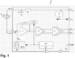
- Fig. 1 illustrated circuitry E according to the present invention
- digital optical signals S can be received.
- a light-receiving component in the form of a photodiode PD is arranged in front of a signal input terminal P IN signal .
- V CORE For generating an additional supply voltage V CORE , which is smaller than the externally applied supply voltage V Supply , in particular between about 1.0 volt and about 1.5 volts, is in Fig. 1 additionally provided a voltage regulator VR.
- the transimpedance input stage IS is followed by a pre- or intermediate stage PS, by means of which the amplitude of the output signal of the transimpedance input stage IS can be adjusted such that the amplitude of this signal is as large as possible, but the signal itself still has the highest possible degree of signal integrity that is not appreciably jittered by distortion.
- this memory controller MC which is assigned an interface or interface IF for setting and / or changing digital values, the signal input terminal P IN signal for specific logic levels, in particular for logic "0” or for logic "1", of the incoming unipolar current signal I PD .
- the current-to-digital-to-analog converter IDAC is acted upon by the digital register MM, MC with a static digital signal in the form of a multi-bit data word.
- the current digital-to-analog converter IDAC converts the (digital) information contained in this data word into the (analogue) D [irect] C [urrent] compensation current I DC ; in other words, the D [irect] C [urrent] compensation current I DC of the current-to-digital-to-analog converter IDAC is set and defined by this data word.
- the 9-bit programmable current-digital-to-analog converter IDAC is connected between the memory module MM of the digital register MM, MC, the signal input terminal P IN signal and the reference or reference potential GND.
- a 2-bit programmable voltage-digital-to-analog converter VDAC may be connected between the memory module MM and the input terminal of the input stage IS in order to amplify (so-called TIA gain) the transimpedance Input stage IS adapt, in particular to control and / or to regulate.
- circuit arrangement E equipped according to the present invention as a high-speed opto-coupler or high-speed opto-coupler, it is possible to use any digital data streams S, for example uncoded video signals, of an optical transmission path from zero bits per second to the high Gbit / s. Area to be received.
- the circuit arrangement E can be part of the connection of two devices in a central office environment, for example at least one server with at least one network storage device (network storage device).
- network storage device network storage device
Landscapes
- Physics & Mathematics (AREA)
- Electromagnetism (AREA)
- Engineering & Computer Science (AREA)
- Computer Networks & Wireless Communication (AREA)
- Signal Processing (AREA)
- Optical Communication System (AREA)
- Amplifiers (AREA)
- Control Of Amplification And Gain Control (AREA)
Applications Claiming Priority (2)
| Application Number | Priority Date | Filing Date | Title |
|---|---|---|---|
| DE102012104420 | 2012-05-22 | ||
| PCT/DE2013/200015 WO2013174376A2 (de) | 2012-05-22 | 2013-05-22 | Schaltungsanordnung und verfahren zum empfangen digitaler optischer signale |
Publications (2)
| Publication Number | Publication Date |
|---|---|
| EP2853046A2 EP2853046A2 (de) | 2015-04-01 |
| EP2853046B1 true EP2853046B1 (de) | 2018-09-26 |
Family
ID=49115336
Family Applications (1)
| Application Number | Title | Priority Date | Filing Date |
|---|---|---|---|
| EP13756810.1A Active EP2853046B1 (de) | 2012-05-22 | 2013-05-22 | Schaltungsanordnung und verfahren zum empfangen digitaler optischer signale |
Country Status (5)
| Country | Link |
|---|---|
| US (1) | US9425901B2 (https=) |
| EP (1) | EP2853046B1 (https=) |
| JP (1) | JP2015517774A (https=) |
| DE (1) | DE112013002641A5 (https=) |
| WO (1) | WO2013174376A2 (https=) |
Families Citing this family (4)
| Publication number | Priority date | Publication date | Assignee | Title |
|---|---|---|---|---|
| EP2744054B1 (en) * | 2012-12-11 | 2018-02-07 | Tyco Electronics Svenska Holdings AB | Interconnect structure for coupling an electronic unit and an optical unit, and optoelectronic module |
| US10097266B2 (en) * | 2017-02-10 | 2018-10-09 | Futurewei Technologies, Inc. | Threshold adjustment compensation of asymmetrical optical noise |
| CN112118052B (zh) | 2019-06-21 | 2021-12-17 | 华为技术有限公司 | 光接收组件、光收发组件、光模块以及光网络设备 |
| CN110707520B (zh) * | 2019-09-20 | 2021-01-08 | 武汉光迅科技股份有限公司 | 一种直调激光器的驱动电路和直调光发射机 |
Family Cites Families (11)
| Publication number | Priority date | Publication date | Assignee | Title |
|---|---|---|---|---|
| NL9301026A (nl) * | 1993-06-11 | 1995-01-02 | Nederland Ptt | Optisch Ontvangsysteem. |
| JPH11205048A (ja) * | 1998-01-14 | 1999-07-30 | Nec Corp | 半導体回路 |
| US6720830B2 (en) * | 2001-06-11 | 2004-04-13 | Johns Hopkins University | Low-power, differential optical receiver in silicon on insulator |
| US20030156774A1 (en) * | 2002-02-15 | 2003-08-21 | Jan Conradi | Unipolar electrical to bipolar optical converter |
| US6911921B2 (en) | 2003-09-19 | 2005-06-28 | International Business Machines Corporation | 5B/6B-T, 3B/4B-T and partitioned 8B/10B-T and 10B/12B transmission codes, and their implementation for high operating rates |
| JP5176505B2 (ja) * | 2007-12-03 | 2013-04-03 | 富士通オプティカルコンポーネンツ株式会社 | 光受信装置,光局側装置および光ネットワークシステム |
| JP5176917B2 (ja) * | 2008-12-05 | 2013-04-03 | 三菱電機株式会社 | 前置増幅器 |
| JP2010178256A (ja) * | 2009-02-02 | 2010-08-12 | Nippon Telegr & Teleph Corp <Ntt> | 光受信器の増幅器 |
| US8238761B2 (en) * | 2009-12-09 | 2012-08-07 | Oracle America, Inc. | Optical receiver with a calibration mode |
| US8155538B2 (en) * | 2009-12-09 | 2012-04-10 | Oracle America, Inc. | Technique for calibrating and centering an optical receiver |
| JP2011249863A (ja) * | 2010-05-21 | 2011-12-08 | Mitsubishi Electric Corp | 親局装置および光信号受信方法 |
-
2013
- 2013-05-22 WO PCT/DE2013/200015 patent/WO2013174376A2/de not_active Ceased
- 2013-05-22 DE DE112013002641.4T patent/DE112013002641A5/de not_active Withdrawn
- 2013-05-22 EP EP13756810.1A patent/EP2853046B1/de active Active
- 2013-05-22 JP JP2015513017A patent/JP2015517774A/ja active Pending
-
2014
- 2014-11-24 US US14/552,159 patent/US9425901B2/en active Active
Non-Patent Citations (1)
| Title |
|---|
| None * |
Also Published As
| Publication number | Publication date |
|---|---|
| WO2013174376A3 (de) | 2014-01-16 |
| EP2853046A2 (de) | 2015-04-01 |
| JP2015517774A (ja) | 2015-06-22 |
| US20150162992A1 (en) | 2015-06-11 |
| US9425901B2 (en) | 2016-08-23 |
| WO2013174376A2 (de) | 2013-11-28 |
| DE112013002641A5 (de) | 2015-02-19 |
Similar Documents
| Publication | Publication Date | Title |
|---|---|---|
| DE69429223T2 (de) | Verfahren zur Parallelimpedanzanpassung für einen Sender und/oder Empfänger, sowie eine integrierte Schaltung und ein Übertragungssystem zur Durchführung des Verfahrens | |
| DE69533625T2 (de) | Anschlussvorrichtung in einer abschlussschaltung | |
| DE102009039414A1 (de) | Hochgeschwindigkeits-Digital-Galvanik-Isolator mit integrierter Niederspannungs-Differentialsignal-Schnittstelle | |
| EP2853046B1 (de) | Schaltungsanordnung und verfahren zum empfangen digitaler optischer signale | |
| DE2320306A1 (de) | Digitale uebertragungsanlage mit einem variablen entzerrer | |
| EP1622257A1 (de) | Verstärkerschaltung zur Umwandlung des Stromsignals eines optischen Empfangselements in ein Spannungssignal | |
| DE102010016974A1 (de) | Justierung von Inter-Pair-Signalversatz | |
| DE102007034574A1 (de) | Datenempfänger und Verfahren zum Verarbeiten von empfangenen Daten | |
| DE19820248B4 (de) | Ausgangspufferschaltkreis mit umschaltbarem Ausgangs-Gleichtaktpegel | |
| DE102005038894B4 (de) | Verfahren zum Empfangen eines optischen Signals und optisches Empfängersystem | |
| DE102014213788A1 (de) | Treiberschaltung für eine Signalübertragung und Steuerverfahren der Treiberschaltung | |
| DE1762829A1 (de) | Selbsteinstellender Analog-Digitalwandler | |
| DE19820643B4 (de) | Taktimpulsübertragungsschaltung | |
| DE10135113B4 (de) | Pseudo-differentieller Leistungstreiber zur Verstärkung eines differentiellen Eingangsstroms | |
| DE102022127378A1 (de) | Verstärkung und zielverstärkung tuning in einem empfänger | |
| DE102008057627B4 (de) | Empfängerschaltung für ein differentielles Eingangssignal und Transceiverschaltung für ein Bussystem | |
| DE102007015643B4 (de) | Verfahren und Vorrichtung zum Übertragen von ausgehenden Nutzsignalen und eines ausgehenden Taktsignals | |
| DE102014109716B4 (de) | Ein Stossbetriebsempfänger, welcher einen großen Dynamikbereich und niedrige Pulsweitenverzerrung hat und ein Verfahren | |
| DE102018220069A1 (de) | Reflexionsdämpfungsvorrichtung für einen Bus eines Bussystems und Verfahren zum Dämpfen von Reflexionen bei einer Datenübertragung in einem Bussystem | |
| DE102019125538A1 (de) | Bus-Treiber für CAN-Busse mit einem buszustandsgesteuerten, beschleunigten Übergang vom dominanten zum rezessiven Datenbuszustand und speziellen Spannungsquellen | |
| EP3039681B1 (de) | Pegelwandlerschaltung | |
| DE102012202298B4 (de) | Vorrichtung und Verfahren zum Treiben von langen Signalleitungen in integrierten Schaltungen | |
| EP0037940A1 (de) | Schaltungsanordnung zum zweidrähtigen Anschluss eines Fernsprechteilnehmers an je eine Leitung für abgehende und ankommende Signale | |
| EP0415209A2 (de) | Schaltungsanordnung zur Regelung des Pegels elektrischer Signale | |
| DE102008057623B4 (de) | Senderschaltung zum Senden eines differentiellen Signals über ein Bussystem und Transceiverschaltung mit einer solchen Senderschaltung |
Legal Events
| Date | Code | Title | Description |
|---|---|---|---|
| PUAI | Public reference made under article 153(3) epc to a published international application that has entered the european phase |
Free format text: ORIGINAL CODE: 0009012 |
|
| 17P | Request for examination filed |
Effective date: 20141222 |
|
| AK | Designated contracting states |
Kind code of ref document: A2 Designated state(s): AL AT BE BG CH CY CZ DE DK EE ES FI FR GB GR HR HU IE IS IT LI LT LU LV MC MK MT NL NO PL PT RO RS SE SI SK SM TR |
|
| AX | Request for extension of the european patent |
Extension state: BA ME |
|
| DAX | Request for extension of the european patent (deleted) | ||
| RAP1 | Party data changed (applicant data changed or rights of an application transferred) |
Owner name: SILICON LINE GMBH |
|
| GRAP | Despatch of communication of intention to grant a patent |
Free format text: ORIGINAL CODE: EPIDOSNIGR1 |
|
| STAA | Information on the status of an ep patent application or granted ep patent |
Free format text: STATUS: GRANT OF PATENT IS INTENDED |
|
| INTG | Intention to grant announced |
Effective date: 20180410 |
|
| GRAS | Grant fee paid |
Free format text: ORIGINAL CODE: EPIDOSNIGR3 |
|
| GRAA | (expected) grant |
Free format text: ORIGINAL CODE: 0009210 |
|
| STAA | Information on the status of an ep patent application or granted ep patent |
Free format text: STATUS: THE PATENT HAS BEEN GRANTED |
|
| AK | Designated contracting states |
Kind code of ref document: B1 Designated state(s): AL AT BE BG CH CY CZ DE DK EE ES FI FR GB GR HR HU IE IS IT LI LT LU LV MC MK MT NL NO PL PT RO RS SE SI SK SM TR |
|
| REG | Reference to a national code |
Ref country code: GB Ref legal event code: FG4D Free format text: NOT ENGLISH |
|
| REG | Reference to a national code |
Ref country code: CH Ref legal event code: EP |
|
| REG | Reference to a national code |
Ref country code: AT Ref legal event code: REF Ref document number: 1047268 Country of ref document: AT Kind code of ref document: T Effective date: 20181015 |
|
| REG | Reference to a national code |
Ref country code: IE Ref legal event code: FG4D Free format text: LANGUAGE OF EP DOCUMENT: GERMAN |
|
| REG | Reference to a national code |
Ref country code: DE Ref legal event code: R096 Ref document number: 502013011187 Country of ref document: DE |
|
| REG | Reference to a national code |
Ref country code: NL Ref legal event code: MP Effective date: 20180926 |
|
| PG25 | Lapsed in a contracting state [announced via postgrant information from national office to epo] |
Ref country code: NO Free format text: LAPSE BECAUSE OF FAILURE TO SUBMIT A TRANSLATION OF THE DESCRIPTION OR TO PAY THE FEE WITHIN THE PRESCRIBED TIME-LIMIT Effective date: 20181226 Ref country code: GR Free format text: LAPSE BECAUSE OF FAILURE TO SUBMIT A TRANSLATION OF THE DESCRIPTION OR TO PAY THE FEE WITHIN THE PRESCRIBED TIME-LIMIT Effective date: 20181227 Ref country code: SE Free format text: LAPSE BECAUSE OF FAILURE TO SUBMIT A TRANSLATION OF THE DESCRIPTION OR TO PAY THE FEE WITHIN THE PRESCRIBED TIME-LIMIT Effective date: 20180926 Ref country code: FI Free format text: LAPSE BECAUSE OF FAILURE TO SUBMIT A TRANSLATION OF THE DESCRIPTION OR TO PAY THE FEE WITHIN THE PRESCRIBED TIME-LIMIT Effective date: 20180926 Ref country code: LT Free format text: LAPSE BECAUSE OF FAILURE TO SUBMIT A TRANSLATION OF THE DESCRIPTION OR TO PAY THE FEE WITHIN THE PRESCRIBED TIME-LIMIT Effective date: 20180926 Ref country code: RS Free format text: LAPSE BECAUSE OF FAILURE TO SUBMIT A TRANSLATION OF THE DESCRIPTION OR TO PAY THE FEE WITHIN THE PRESCRIBED TIME-LIMIT Effective date: 20180926 Ref country code: BG Free format text: LAPSE BECAUSE OF FAILURE TO SUBMIT A TRANSLATION OF THE DESCRIPTION OR TO PAY THE FEE WITHIN THE PRESCRIBED TIME-LIMIT Effective date: 20181226 |
|
| REG | Reference to a national code |
Ref country code: LT Ref legal event code: MG4D |
|
| PG25 | Lapsed in a contracting state [announced via postgrant information from national office to epo] |
Ref country code: AL Free format text: LAPSE BECAUSE OF FAILURE TO SUBMIT A TRANSLATION OF THE DESCRIPTION OR TO PAY THE FEE WITHIN THE PRESCRIBED TIME-LIMIT Effective date: 20180926 Ref country code: LV Free format text: LAPSE BECAUSE OF FAILURE TO SUBMIT A TRANSLATION OF THE DESCRIPTION OR TO PAY THE FEE WITHIN THE PRESCRIBED TIME-LIMIT Effective date: 20180926 Ref country code: HR Free format text: LAPSE BECAUSE OF FAILURE TO SUBMIT A TRANSLATION OF THE DESCRIPTION OR TO PAY THE FEE WITHIN THE PRESCRIBED TIME-LIMIT Effective date: 20180926 |
|
| PG25 | Lapsed in a contracting state [announced via postgrant information from national office to epo] |
Ref country code: IS Free format text: LAPSE BECAUSE OF FAILURE TO SUBMIT A TRANSLATION OF THE DESCRIPTION OR TO PAY THE FEE WITHIN THE PRESCRIBED TIME-LIMIT Effective date: 20190126 Ref country code: NL Free format text: LAPSE BECAUSE OF FAILURE TO SUBMIT A TRANSLATION OF THE DESCRIPTION OR TO PAY THE FEE WITHIN THE PRESCRIBED TIME-LIMIT Effective date: 20180926 Ref country code: PL Free format text: LAPSE BECAUSE OF FAILURE TO SUBMIT A TRANSLATION OF THE DESCRIPTION OR TO PAY THE FEE WITHIN THE PRESCRIBED TIME-LIMIT Effective date: 20180926 Ref country code: ES Free format text: LAPSE BECAUSE OF FAILURE TO SUBMIT A TRANSLATION OF THE DESCRIPTION OR TO PAY THE FEE WITHIN THE PRESCRIBED TIME-LIMIT Effective date: 20180926 Ref country code: CZ Free format text: LAPSE BECAUSE OF FAILURE TO SUBMIT A TRANSLATION OF THE DESCRIPTION OR TO PAY THE FEE WITHIN THE PRESCRIBED TIME-LIMIT Effective date: 20180926 Ref country code: RO Free format text: LAPSE BECAUSE OF FAILURE TO SUBMIT A TRANSLATION OF THE DESCRIPTION OR TO PAY THE FEE WITHIN THE PRESCRIBED TIME-LIMIT Effective date: 20180926 Ref country code: IT Free format text: LAPSE BECAUSE OF FAILURE TO SUBMIT A TRANSLATION OF THE DESCRIPTION OR TO PAY THE FEE WITHIN THE PRESCRIBED TIME-LIMIT Effective date: 20180926 Ref country code: EE Free format text: LAPSE BECAUSE OF FAILURE TO SUBMIT A TRANSLATION OF THE DESCRIPTION OR TO PAY THE FEE WITHIN THE PRESCRIBED TIME-LIMIT Effective date: 20180926 |
|
| PG25 | Lapsed in a contracting state [announced via postgrant information from national office to epo] |
Ref country code: PT Free format text: LAPSE BECAUSE OF FAILURE TO SUBMIT A TRANSLATION OF THE DESCRIPTION OR TO PAY THE FEE WITHIN THE PRESCRIBED TIME-LIMIT Effective date: 20190126 Ref country code: SM Free format text: LAPSE BECAUSE OF FAILURE TO SUBMIT A TRANSLATION OF THE DESCRIPTION OR TO PAY THE FEE WITHIN THE PRESCRIBED TIME-LIMIT Effective date: 20180926 Ref country code: SK Free format text: LAPSE BECAUSE OF FAILURE TO SUBMIT A TRANSLATION OF THE DESCRIPTION OR TO PAY THE FEE WITHIN THE PRESCRIBED TIME-LIMIT Effective date: 20180926 |
|
| REG | Reference to a national code |
Ref country code: DE Ref legal event code: R097 Ref document number: 502013011187 Country of ref document: DE |
|
| PG25 | Lapsed in a contracting state [announced via postgrant information from national office to epo] |
Ref country code: DK Free format text: LAPSE BECAUSE OF FAILURE TO SUBMIT A TRANSLATION OF THE DESCRIPTION OR TO PAY THE FEE WITHIN THE PRESCRIBED TIME-LIMIT Effective date: 20180926 |
|
| PLBE | No opposition filed within time limit |
Free format text: ORIGINAL CODE: 0009261 |
|
| STAA | Information on the status of an ep patent application or granted ep patent |
Free format text: STATUS: NO OPPOSITION FILED WITHIN TIME LIMIT |
|
| 26N | No opposition filed |
Effective date: 20190627 |
|
| PG25 | Lapsed in a contracting state [announced via postgrant information from national office to epo] |
Ref country code: SI Free format text: LAPSE BECAUSE OF FAILURE TO SUBMIT A TRANSLATION OF THE DESCRIPTION OR TO PAY THE FEE WITHIN THE PRESCRIBED TIME-LIMIT Effective date: 20180926 |
|
| PG25 | Lapsed in a contracting state [announced via postgrant information from national office to epo] |
Ref country code: MC Free format text: LAPSE BECAUSE OF FAILURE TO SUBMIT A TRANSLATION OF THE DESCRIPTION OR TO PAY THE FEE WITHIN THE PRESCRIBED TIME-LIMIT Effective date: 20180926 |
|
| PG25 | Lapsed in a contracting state [announced via postgrant information from national office to epo] |
Ref country code: LU Free format text: LAPSE BECAUSE OF NON-PAYMENT OF DUE FEES Effective date: 20190522 |
|
| PG25 | Lapsed in a contracting state [announced via postgrant information from national office to epo] |
Ref country code: TR Free format text: LAPSE BECAUSE OF FAILURE TO SUBMIT A TRANSLATION OF THE DESCRIPTION OR TO PAY THE FEE WITHIN THE PRESCRIBED TIME-LIMIT Effective date: 20180926 |
|
| PG25 | Lapsed in a contracting state [announced via postgrant information from national office to epo] |
Ref country code: IE Free format text: LAPSE BECAUSE OF NON-PAYMENT OF DUE FEES Effective date: 20190522 |
|
| REG | Reference to a national code |
Ref country code: AT Ref legal event code: MM01 Ref document number: 1047268 Country of ref document: AT Kind code of ref document: T Effective date: 20190522 |
|
| PG25 | Lapsed in a contracting state [announced via postgrant information from national office to epo] |
Ref country code: AT Free format text: LAPSE BECAUSE OF NON-PAYMENT OF DUE FEES Effective date: 20190522 |
|
| PG25 | Lapsed in a contracting state [announced via postgrant information from national office to epo] |
Ref country code: CY Free format text: LAPSE BECAUSE OF FAILURE TO SUBMIT A TRANSLATION OF THE DESCRIPTION OR TO PAY THE FEE WITHIN THE PRESCRIBED TIME-LIMIT Effective date: 20180926 |
|
| PG25 | Lapsed in a contracting state [announced via postgrant information from national office to epo] |
Ref country code: MT Free format text: LAPSE BECAUSE OF FAILURE TO SUBMIT A TRANSLATION OF THE DESCRIPTION OR TO PAY THE FEE WITHIN THE PRESCRIBED TIME-LIMIT Effective date: 20180926 Ref country code: HU Free format text: LAPSE BECAUSE OF FAILURE TO SUBMIT A TRANSLATION OF THE DESCRIPTION OR TO PAY THE FEE WITHIN THE PRESCRIBED TIME-LIMIT; INVALID AB INITIO Effective date: 20130522 |
|
| PGFP | Annual fee paid to national office [announced via postgrant information from national office to epo] |
Ref country code: CH Payment date: 20210830 Year of fee payment: 9 |
|
| PG25 | Lapsed in a contracting state [announced via postgrant information from national office to epo] |
Ref country code: MK Free format text: LAPSE BECAUSE OF FAILURE TO SUBMIT A TRANSLATION OF THE DESCRIPTION OR TO PAY THE FEE WITHIN THE PRESCRIBED TIME-LIMIT Effective date: 20180926 |
|
| REG | Reference to a national code |
Ref country code: CH Ref legal event code: PL |
|
| PG25 | Lapsed in a contracting state [announced via postgrant information from national office to epo] |
Ref country code: LI Free format text: LAPSE BECAUSE OF NON-PAYMENT OF DUE FEES Effective date: 20220531 Ref country code: CH Free format text: LAPSE BECAUSE OF NON-PAYMENT OF DUE FEES Effective date: 20220531 |
|
| P01 | Opt-out of the competence of the unified patent court (upc) registered |
Effective date: 20230527 |
|
| PGFP | Annual fee paid to national office [announced via postgrant information from national office to epo] |
Ref country code: BE Payment date: 20230530 Year of fee payment: 11 |
|
| PGFP | Annual fee paid to national office [announced via postgrant information from national office to epo] |
Ref country code: GB Payment date: 20230630 Year of fee payment: 11 |
|
| GBPC | Gb: european patent ceased through non-payment of renewal fee |
Effective date: 20240522 |
|
| REG | Reference to a national code |
Ref country code: BE Ref legal event code: MM Effective date: 20240531 |
|
| PG25 | Lapsed in a contracting state [announced via postgrant information from national office to epo] |
Ref country code: BE Free format text: LAPSE BECAUSE OF NON-PAYMENT OF DUE FEES Effective date: 20240531 |
|
| PG25 | Lapsed in a contracting state [announced via postgrant information from national office to epo] |
Ref country code: GB Free format text: LAPSE BECAUSE OF NON-PAYMENT OF DUE FEES Effective date: 20240522 |
|
| PGFP | Annual fee paid to national office [announced via postgrant information from national office to epo] |
Ref country code: FR Payment date: 20250602 Year of fee payment: 13 |
|
| PGFP | Annual fee paid to national office [announced via postgrant information from national office to epo] |
Ref country code: DE Payment date: 20250731 Year of fee payment: 13 |