EP2849340A1 - Verstärkerschaltung - Google Patents
Verstärkerschaltung Download PDFInfo
- Publication number
- EP2849340A1 EP2849340A1 EP14191591.8A EP14191591A EP2849340A1 EP 2849340 A1 EP2849340 A1 EP 2849340A1 EP 14191591 A EP14191591 A EP 14191591A EP 2849340 A1 EP2849340 A1 EP 2849340A1
- Authority
- EP
- European Patent Office
- Prior art keywords
- amplifier
- circuit
- resistance
- input
- amplifiers
- Prior art date
- Legal status (The legal status is an assumption and is not a legal conclusion. Google has not performed a legal analysis and makes no representation as to the accuracy of the status listed.)
- Withdrawn
Links
- 239000003990 capacitor Substances 0.000 claims description 72
- 230000004044 response Effects 0.000 abstract description 90
- 210000003127 knee Anatomy 0.000 abstract description 4
- 230000003321 amplification Effects 0.000 description 17
- 230000008859 change Effects 0.000 description 17
- 238000003199 nucleic acid amplification method Methods 0.000 description 17
- 230000000694 effects Effects 0.000 description 9
- 230000007423 decrease Effects 0.000 description 8
- 238000013016 damping Methods 0.000 description 6
- 230000003247 decreasing effect Effects 0.000 description 5
- 238000013461 design Methods 0.000 description 5
- 230000006866 deterioration Effects 0.000 description 4
- 238000012360 testing method Methods 0.000 description 3
- 230000008901 benefit Effects 0.000 description 2
- 239000000919 ceramic Substances 0.000 description 2
- 238000010168 coupling process Methods 0.000 description 2
- 238000005859 coupling reaction Methods 0.000 description 2
- 230000009977 dual effect Effects 0.000 description 2
- 238000000034 method Methods 0.000 description 2
- 230000003139 buffering effect Effects 0.000 description 1
- 230000008878 coupling Effects 0.000 description 1
- 230000005669 field effect Effects 0.000 description 1
- 238000009413 insulation Methods 0.000 description 1
- 238000005259 measurement Methods 0.000 description 1
- 230000010355 oscillation Effects 0.000 description 1
- 239000004065 semiconductor Substances 0.000 description 1
- 238000012546 transfer Methods 0.000 description 1
- 238000009966 trimming Methods 0.000 description 1
Images


Classifications
-
- H—ELECTRICITY
- H03—ELECTRONIC CIRCUITRY
- H03F—AMPLIFIERS
- H03F1/00—Details of amplifiers with only discharge tubes, only semiconductor devices or only unspecified devices as amplifying elements
- H03F1/34—Negative-feedback-circuit arrangements with or without positive feedback
-
- H—ELECTRICITY
- H03—ELECTRONIC CIRCUITRY
- H03F—AMPLIFIERS
- H03F1/00—Details of amplifiers with only discharge tubes, only semiconductor devices or only unspecified devices as amplifying elements
- H03F1/42—Modifications of amplifiers to extend the bandwidth
- H03F1/48—Modifications of amplifiers to extend the bandwidth of aperiodic amplifiers
- H03F1/486—Modifications of amplifiers to extend the bandwidth of aperiodic amplifiers with IC amplifier blocks
-
- H—ELECTRICITY
- H03—ELECTRONIC CIRCUITRY
- H03F—AMPLIFIERS
- H03F3/00—Amplifiers with only discharge tubes or only semiconductor devices as amplifying elements
- H03F3/04—Amplifiers with only discharge tubes or only semiconductor devices as amplifying elements with semiconductor devices only
- H03F3/08—Amplifiers with only discharge tubes or only semiconductor devices as amplifying elements with semiconductor devices only controlled by light
- H03F3/087—Amplifiers with only discharge tubes or only semiconductor devices as amplifying elements with semiconductor devices only controlled by light with IC amplifier blocks
-
- H—ELECTRICITY
- H03—ELECTRONIC CIRCUITRY
- H03F—AMPLIFIERS
- H03F3/00—Amplifiers with only discharge tubes or only semiconductor devices as amplifying elements
- H03F3/20—Power amplifiers, e.g. Class B amplifiers, Class C amplifiers
- H03F3/21—Power amplifiers, e.g. Class B amplifiers, Class C amplifiers with semiconductor devices only
- H03F3/211—Power amplifiers, e.g. Class B amplifiers, Class C amplifiers with semiconductor devices only using a combination of several amplifiers
-
- H—ELECTRICITY
- H03—ELECTRONIC CIRCUITRY
- H03F—AMPLIFIERS
- H03F3/00—Amplifiers with only discharge tubes or only semiconductor devices as amplifying elements
- H03F3/45—Differential amplifiers
- H03F3/45071—Differential amplifiers with semiconductor devices only
- H03F3/45076—Differential amplifiers with semiconductor devices only characterised by the way of implementation of the active amplifying circuit in the differential amplifier
- H03F3/45475—Differential amplifiers with semiconductor devices only characterised by the way of implementation of the active amplifying circuit in the differential amplifier using IC blocks as the active amplifying circuit
-
- H—ELECTRICITY
- H03—ELECTRONIC CIRCUITRY
- H03F—AMPLIFIERS
- H03F2200/00—Indexing scheme relating to amplifiers
- H03F2200/135—Indexing scheme relating to amplifiers there being a feedback over one or more internal stages in the global amplifier
-
- H—ELECTRICITY
- H03—ELECTRONIC CIRCUITRY
- H03F—AMPLIFIERS
- H03F2200/00—Indexing scheme relating to amplifiers
- H03F2200/144—Indexing scheme relating to amplifiers the feedback circuit of the amplifier stage comprising a passive resistor and passive capacitor
-
- H—ELECTRICITY
- H03—ELECTRONIC CIRCUITRY
- H03F—AMPLIFIERS
- H03F2200/00—Indexing scheme relating to amplifiers
- H03F2200/261—Amplifier which being suitable for instrumentation applications
-
- H—ELECTRICITY
- H03—ELECTRONIC CIRCUITRY
- H03F—AMPLIFIERS
- H03F2200/00—Indexing scheme relating to amplifiers
- H03F2200/36—Indexing scheme relating to amplifiers the amplifier comprising means for increasing the bandwidth
-
- H—ELECTRICITY
- H03—ELECTRONIC CIRCUITRY
- H03F—AMPLIFIERS
- H03F2200/00—Indexing scheme relating to amplifiers
- H03F2200/405—Indexing scheme relating to amplifiers the output amplifying stage of an amplifier comprising more than three power stages
-
- H—ELECTRICITY
- H03—ELECTRONIC CIRCUITRY
- H03F—AMPLIFIERS
- H03F2200/00—Indexing scheme relating to amplifiers
- H03F2200/408—Indexing scheme relating to amplifiers the output amplifying stage of an amplifier comprising three power stages
-
- H—ELECTRICITY
- H03—ELECTRONIC CIRCUITRY
- H03F—AMPLIFIERS
- H03F2200/00—Indexing scheme relating to amplifiers
- H03F2200/411—Indexing scheme relating to amplifiers the output amplifying stage of an amplifier comprising two power stages
-
- H—ELECTRICITY
- H03—ELECTRONIC CIRCUITRY
- H03F—AMPLIFIERS
- H03F2203/00—Indexing scheme relating to amplifiers with only discharge tubes or only semiconductor devices as amplifying elements covered by H03F3/00
- H03F2203/45—Indexing scheme relating to differential amplifiers
- H03F2203/45138—Two or more differential amplifiers in IC-block form are combined, e.g. measuring amplifiers
-
- H—ELECTRICITY
- H03—ELECTRONIC CIRCUITRY
- H03F—AMPLIFIERS
- H03F2203/00—Indexing scheme relating to amplifiers with only discharge tubes or only semiconductor devices as amplifying elements covered by H03F3/00
- H03F2203/45—Indexing scheme relating to differential amplifiers
- H03F2203/45512—Indexing scheme relating to differential amplifiers the FBC comprising one or more capacitors, not being switched capacitors, and being coupled between the LC and the IC
-
- H—ELECTRICITY
- H03—ELECTRONIC CIRCUITRY
- H03F—AMPLIFIERS
- H03F2203/00—Indexing scheme relating to amplifiers with only discharge tubes or only semiconductor devices as amplifying elements covered by H03F3/00
- H03F2203/45—Indexing scheme relating to differential amplifiers
- H03F2203/45526—Indexing scheme relating to differential amplifiers the FBC comprising a resistor-capacitor combination and being coupled between the LC and the IC
-
- H—ELECTRICITY
- H03—ELECTRONIC CIRCUITRY
- H03F—AMPLIFIERS
- H03F2203/00—Indexing scheme relating to amplifiers with only discharge tubes or only semiconductor devices as amplifying elements covered by H03F3/00
- H03F2203/45—Indexing scheme relating to differential amplifiers
- H03F2203/45528—Indexing scheme relating to differential amplifiers the FBC comprising one or more passive resistors and being coupled between the LC and the IC
-
- H—ELECTRICITY
- H03—ELECTRONIC CIRCUITRY
- H03F—AMPLIFIERS
- H03F2203/00—Indexing scheme relating to amplifiers with only discharge tubes or only semiconductor devices as amplifying elements covered by H03F3/00
- H03F2203/45—Indexing scheme relating to differential amplifiers
- H03F2203/45536—Indexing scheme relating to differential amplifiers the FBC comprising a switch and being coupled between the LC and the IC
-
- H—ELECTRICITY
- H03—ELECTRONIC CIRCUITRY
- H03F—AMPLIFIERS
- H03F2203/00—Indexing scheme relating to amplifiers with only discharge tubes or only semiconductor devices as amplifying elements covered by H03F3/00
- H03F2203/45—Indexing scheme relating to differential amplifiers
- H03F2203/45544—Indexing scheme relating to differential amplifiers the IC comprising one or more capacitors, e.g. coupling capacitors
-
- H—ELECTRICITY
- H03—ELECTRONIC CIRCUITRY
- H03F—AMPLIFIERS
- H03F2203/00—Indexing scheme relating to amplifiers with only discharge tubes or only semiconductor devices as amplifying elements covered by H03F3/00
- H03F2203/45—Indexing scheme relating to differential amplifiers
- H03F2203/45548—Indexing scheme relating to differential amplifiers the IC comprising one or more capacitors as shunts to earth or as short circuit between inputs
-
- H—ELECTRICITY
- H03—ELECTRONIC CIRCUITRY
- H03F—AMPLIFIERS
- H03F2203/00—Indexing scheme relating to amplifiers with only discharge tubes or only semiconductor devices as amplifying elements covered by H03F3/00
- H03F2203/45—Indexing scheme relating to differential amplifiers
- H03F2203/45594—Indexing scheme relating to differential amplifiers the IC comprising one or more resistors, which are not biasing resistor
-
- H—ELECTRICITY
- H03—ELECTRONIC CIRCUITRY
- H03F—AMPLIFIERS
- H03F2203/00—Indexing scheme relating to amplifiers with only discharge tubes or only semiconductor devices as amplifying elements covered by H03F3/00
- H03F2203/45—Indexing scheme relating to differential amplifiers
- H03F2203/45612—Indexing scheme relating to differential amplifiers the IC comprising one or more input source followers as input stages in the IC
Definitions
- the present invention relates to an amplifier circuit of a current amplifier, a voltage amplifier, a charge amplifier, a transimpedance amplifier for a photodiode, etc.
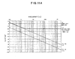
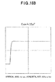
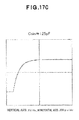
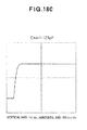
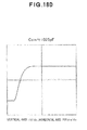
- FIGS. 16B to 16D depict it that an overshoot is introduced into the waveform of pulse response when the inverting input capacitance Csin is large under the condition that the feedback capacitance Cf is set so as to adapt the small inverting input capacitance Csin. Conversely, FIGS.
- Terminal capacitance C SRf of the feedback resistance Rf affects the bandwidth fc to narrow.
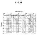
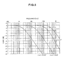
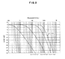
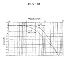
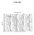
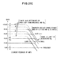
- FIG. 21F depicts an example of achieving a broadband of the amplifier depicted in FIG. 1A in the form of the frequency response of the open loop gain.
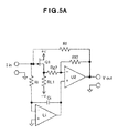
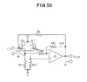
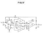
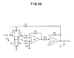
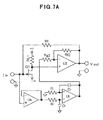
- FIG. 5B illustrates utilizing a voltage follower using an op-amp as an example of this buffer amplifier Ub.
- signal output of a FET Q1 is inverted and amplified at the op-amp U2 near the output, and the output of the integrator Ui is non-inverted and amplified at the op-amp U2 near the output.
- the signal of the FET Q1 and the output of the integrator Ui that is, compensating voltage is summed with reverse polarity.
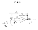
- FIGS. 5C to 5H illustrates the configuration of utilizing the source follower using a FET, and a circuit of the same circuit configuration as this source follower using a FET, fixing the input potential of this circuit, subtracting the gate-source voltage V GS of the source follower using a FET, and obtaining compensation.
- a source follower using a FET Q1 functions as the amplifier near the input
- a source follower using a FET Q1' is another circuit, and functions as a circuit of generating compensation voltage.
- offset error and drift can be suppressed by using two FETs of the same properties as far as possible. If these two FETs are thermally-coupled, offset error and drift can be suppressed further.
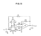
- FIG. 7D depicts an example of compensating the gate-drain voltage V GD of the common source amplifier using a FET at a second-stage common base amplifier using a bipolar transistor, obtaining a single-end using a current mirror, and providing an inverting amplifier using an op-amp at the output side.
- An output buffer is a kind of a non-inverting amplifier whose gain is about 1.
- An output buffer takes the effects of increasing current that the output can drive, and decreasing output impedance.
- the functionality of an output buffer is almost same to the above described follower.
- An IC that is only for the buffering purpose, a voltage follower using an op-amp, and a
- the configuration according to the sixth embodiment can be widely used as resistance whose terminal capacitance is equivalently zero, for feedback resistance and gain resistance which are used for an amplifier, reference resistance for measuring the frequency response of a current amplifier, and another use.
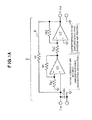
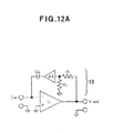
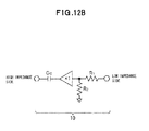
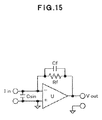
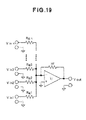
- FIG. 12A illustrates a current amplifier to which the feedback circuit 10 of FIG. 12B is applied.
- "U” in FIG. 12A means the whole plurality of amplifiers, each of which negative feedback is provided to [0157]
- " ⁇ 1" in each of FIGS. 12A and 12B represents a buffer amplifier.
- the output voltage of the current amplifier is divided by the resistances R1 and R2, and this divided voltage is given to the buffer amplifier. Therefore, the amount of a signal that is given to the input of the amplifier through capacitance Cc is also R2 divided by (R1 + R2).
- the feedback circuit works as smaller capacitance equivalent to Cc ⁇ R2 divided by (R1 + R2).
- the feedback circuit 12 whose capacitance Cc is equivalently small capacitance according to the attenuation factor of an attenuator can be also realized if an end of the capacitance Cc is connected to an end of
- the feedback circuit can be used as an adjustable, and smaller capacitance than the capacitance Cc.
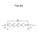
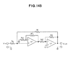
- FIG. 14A illustrates a current amplifier that has the same configuration to FIG. 1A according to the first embodiment.
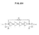
- Fig. 14B illustrates a voltage amplifier that is configured by adding the gain resistance Rg to the configuration of FIG. 14A .
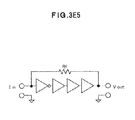
- any configuration according to the second to fifth embodiments can be freely applied to portions where a non-inverting amplifier and an inverting amplifier are connected in series in FIGS. 14A to 14D .
- the feedback resistance Rf in FIGS. 14A to 14D can be also configured by applying the sixth embodiment, or by using the configuration of the seventh embodiment together.
Landscapes
- Engineering & Computer Science (AREA)
- Power Engineering (AREA)
- Amplifiers (AREA)
Applications Claiming Priority (2)
| Application Number | Priority Date | Filing Date | Title |
|---|---|---|---|
| JP2011190462 | 2011-09-01 | ||
| EP12182338.9A EP2566048B1 (de) | 2011-09-01 | 2012-08-30 | Verstärkerschaltung |
Related Parent Applications (2)
| Application Number | Title | Priority Date | Filing Date |
|---|---|---|---|
| EP12182338.9A Division EP2566048B1 (de) | 2011-09-01 | 2012-08-30 | Verstärkerschaltung |
| EP12182338.9A Division-Into EP2566048B1 (de) | 2011-09-01 | 2012-08-30 | Verstärkerschaltung |
Publications (1)
| Publication Number | Publication Date |
|---|---|
| EP2849340A1 true EP2849340A1 (de) | 2015-03-18 |
Family
ID=46796394
Family Applications (2)
| Application Number | Title | Priority Date | Filing Date |
|---|---|---|---|
| EP14191591.8A Withdrawn EP2849340A1 (de) | 2011-09-01 | 2012-08-30 | Verstärkerschaltung |
| EP12182338.9A Active EP2566048B1 (de) | 2011-09-01 | 2012-08-30 | Verstärkerschaltung |
Family Applications After (1)
| Application Number | Title | Priority Date | Filing Date |
|---|---|---|---|
| EP12182338.9A Active EP2566048B1 (de) | 2011-09-01 | 2012-08-30 | Verstärkerschaltung |
Country Status (3)
| Country | Link |
|---|---|
| US (2) | US9024686B2 (de) |
| EP (2) | EP2849340A1 (de) |
| JP (1) | JP6022262B2 (de) |
Cited By (1)
| Publication number | Priority date | Publication date | Assignee | Title |
|---|---|---|---|---|
| EP3367561A1 (de) * | 2017-02-28 | 2018-08-29 | Huawei Technologies Co., Ltd. | Mehrstufiger verstärker mit negativer rückkopplung |
Families Citing this family (21)
| Publication number | Priority date | Publication date | Assignee | Title |
|---|---|---|---|---|
| WO2010079631A1 (ja) * | 2009-01-09 | 2010-07-15 | 三菱電機株式会社 | マルチポートアンプおよびそれを用いた無線装置 |
| US9274145B2 (en) * | 2012-10-22 | 2016-03-01 | Tektronix, Inc. | Active shunt ammeter apparatus and method |
| JP5836921B2 (ja) * | 2012-12-18 | 2015-12-24 | 株式会社東芝 | 電力増幅回路 |
| JP6398056B2 (ja) * | 2013-09-30 | 2018-10-03 | 株式会社エヌエフ回路設計ブロック | 電流帰還型増幅回路 |
| US9453880B2 (en) * | 2014-01-24 | 2016-09-27 | Keithley Instruments, Inc. | Active shunt source-measure unit (SMU) circuit |
| GB2526857B (en) * | 2014-06-05 | 2016-09-07 | Thermo Fisher Scient (Bremen) Gmbh | A transimpedance amplifier |
| JP6296965B2 (ja) | 2014-11-28 | 2018-03-20 | 株式会社アドバンテスト | 電流測定回路および塩基配列解析装置 |
| JP6895224B2 (ja) * | 2016-03-29 | 2021-06-30 | 株式会社エヌエフホールディングス | 光電変換素子用電流増幅装置 |
| US10663490B2 (en) * | 2016-06-30 | 2020-05-26 | Keithley Instruments, Llc | Nested ammeter |
| EP3685506B1 (de) * | 2017-06-13 | 2024-03-06 | Firecomms Limited | Rauscharmer transimpedanzverstärker mit regler |
| WO2019216274A1 (ja) * | 2018-05-08 | 2019-11-14 | 株式会社エヌエフ回路設計ブロック | 静電容量測定回路及び静電容量変位計 |
| CN108600916B (zh) * | 2018-05-14 | 2021-01-01 | 祁家堃 | 音响电路及系统 |
| JP2020027991A (ja) * | 2018-08-10 | 2020-02-20 | 株式会社エヌエフ回路設計ブロック | 電流増幅回路 |
| US10972063B2 (en) | 2018-10-17 | 2021-04-06 | Analog Devices Global Unlimited Company | Amplifier systems for measuring a wide range of current |
| US11431308B2 (en) * | 2019-04-05 | 2022-08-30 | Baker Hughes Oilfield Operations Llc | Differential noise cancellation |
| JP7408129B2 (ja) | 2019-11-25 | 2024-01-05 | 株式会社エヌエフホールディングス | 電荷増幅回路および測定回路 |
| CN112202410B (zh) * | 2020-10-15 | 2024-01-09 | 中国科学院空天信息创新研究院 | 双环路跨阻放大器 |
| CN114184878A (zh) * | 2021-10-27 | 2022-03-15 | 天津工业大学 | 一种断路器短路性能测试电路 |
| WO2023171125A1 (ja) * | 2022-03-11 | 2023-09-14 | ソニーセミコンダクタソリューションズ株式会社 | 低雑音増幅器、および、センサ装置 |
| CN114995576B (zh) * | 2022-05-09 | 2023-09-15 | 贵州振华风光半导体股份有限公司 | 适应低电压工作的双向自偏置双极性电流镜电路 |
| DE102022122333A1 (de) * | 2022-09-02 | 2024-03-07 | WiredSense GmbH | Verstärkerschaltung zur breitbandigen und rauscharmen Verstärkung einer kapazitiven Stromquelle und ein Sensorsystem |
Citations (4)
| Publication number | Priority date | Publication date | Assignee | Title |
|---|---|---|---|---|
| US3918005A (en) * | 1974-07-24 | 1975-11-04 | Bell Telephone Labor Inc | Operational amplifier circuitry with automatic self-biasing for enhanced voltage compliance |
| US5317277A (en) * | 1992-12-08 | 1994-05-31 | Doble Engineering Company | Power amplifying apparatus for supplying A.C. signals having a maximum loop gain at a desired frequency |
| US20030058044A1 (en) * | 2001-09-07 | 2003-03-27 | Candy Bruce Halcro | Amplifier improvements |
| JP2005064903A (ja) | 2003-08-13 | 2005-03-10 | Nf Corp | 広帯域増幅器及びi−v変換器 |
Family Cites Families (18)
| Publication number | Priority date | Publication date | Assignee | Title |
|---|---|---|---|---|
| JPS5323252A (en) * | 1976-08-16 | 1978-03-03 | Yashica Co Ltd | Operational amplifier |
| JPS54160150A (en) * | 1978-06-09 | 1979-12-18 | Nippon Gakki Seizo Kk | Frequency selecting circuit |
| JPS626722Y2 (de) * | 1978-11-16 | 1987-02-17 | ||
| US4540952A (en) * | 1981-09-08 | 1985-09-10 | At&T Bell Laboratories | Nonintegrating receiver |
| JPH0773171B2 (ja) * | 1987-09-30 | 1995-08-02 | 株式会社東芝 | 複合演算増幅回路 |
| JPH0273104A (ja) * | 1988-09-07 | 1990-03-13 | Fuji Electric Co Ltd | 半導体センサの温度補償回路 |
| JPH0440373A (ja) * | 1990-06-05 | 1992-02-10 | Agency Of Ind Science & Technol | 電流電圧変換回路 |
| JPH05268571A (ja) * | 1992-03-23 | 1993-10-15 | Sony Corp | 帰還型ソフトリミッタ |
| JPH07321569A (ja) | 1994-05-19 | 1995-12-08 | Sony Tektronix Corp | 広帯域反転増幅器 |
| JP3225260B2 (ja) | 1996-09-30 | 2001-11-05 | 株式会社ケンウッド | フィルタ回路 |
| JP3166681B2 (ja) | 1997-10-31 | 2001-05-14 | ヤマハ株式会社 | アクティブフィルタおよびアクティブフィルタ用集積回路 |
| JP2001068967A (ja) | 1999-08-30 | 2001-03-16 | Sony Corp | 可変抵抗回路、可変フィルタ回路、それらの調整回路およびこれらを使用した受信機 |
| JP2001068966A (ja) | 1999-08-30 | 2001-03-16 | Sony Corp | フィルタの調整回路およびこれを使用した受信機 |
| JP3638241B2 (ja) * | 2000-01-21 | 2005-04-13 | シャープ株式会社 | 集積増幅回路 |
| JP4184245B2 (ja) | 2003-12-01 | 2008-11-19 | 富士男 小澤 | 電流/電圧変換回路 |
| JP4451415B2 (ja) | 2006-05-29 | 2010-04-14 | 富士男 小澤 | 電流/電圧変換回路 |
| JP5030216B2 (ja) | 2007-06-20 | 2012-09-19 | 日置電機株式会社 | 電流電圧変換回路 |
| US7863977B1 (en) * | 2009-09-14 | 2011-01-04 | Edan Instruments, Inc. | Fully differential non-inverted parallel amplifier for detecting biology electrical signal |
-
2012
- 2012-08-30 JP JP2012189400A patent/JP6022262B2/ja active Active
- 2012-08-30 US US13/599,637 patent/US9024686B2/en active Active
- 2012-08-30 EP EP14191591.8A patent/EP2849340A1/de not_active Withdrawn
- 2012-08-30 EP EP12182338.9A patent/EP2566048B1/de active Active
-
2014
- 2014-01-23 US US14/162,193 patent/US9252720B2/en active Active
Patent Citations (4)
| Publication number | Priority date | Publication date | Assignee | Title |
|---|---|---|---|---|
| US3918005A (en) * | 1974-07-24 | 1975-11-04 | Bell Telephone Labor Inc | Operational amplifier circuitry with automatic self-biasing for enhanced voltage compliance |
| US5317277A (en) * | 1992-12-08 | 1994-05-31 | Doble Engineering Company | Power amplifying apparatus for supplying A.C. signals having a maximum loop gain at a desired frequency |
| US20030058044A1 (en) * | 2001-09-07 | 2003-03-27 | Candy Bruce Halcro | Amplifier improvements |
| JP2005064903A (ja) | 2003-08-13 | 2005-03-10 | Nf Corp | 広帯域増幅器及びi−v変換器 |
Non-Patent Citations (4)
| Title |
|---|
| "Design Considerations for a Transimpedance Amplifier. Application Note 1803", 28 February 2008, NATIONAL SEMICONDUCTOR CORPORATION |
| MENG X R ET AL: "CFA based fully integrated Tow-Thomas biquad", ELECTRONICS LETTERS, IEE STEVENAGE, GB, vol. 32, no. 8, 11 April 1996 (1996-04-11), pages 722 - 723, XP006005026, ISSN: 0013-5194, DOI: 10.1049/EL:19960534 * |
| PICCIRILLI M C: "A fully integrated Tow-Thomas biquad using current feedback amplifiers", ICECS'99. PROCEEDINGS OF ICECS'99. 6TH IEEE INTERNATIONAL CONFERENCE ON ELECTRONICS, CIRCUITS AND SYSTEMS; 5-8 SEPT. 1999; PAFOS, CYPRUS, IEEE, PISCATAWAY, NJ, USA, vol. 3, 5 September 1999 (1999-09-05), pages 1325 - 1328, XP010361847, ISBN: 978-0-7803-5682-5, DOI: 10.1109/ICECS.1999.814413 * |
| YAMAZAKI A ET AL: "An active-RC reconfigurable lowpass-polyphase tow-thomas biquad filter", IEEE INTERNATIONAL MIDWEST SYMPOSIUM, IEEE, vol. 1, 25 July 2004 (2004-07-25), pages 1_57 - 1_60, XP010738961, ISBN: 978-0-7803-8346-3, DOI: 10.1109/MWSCAS.2004.1353896 * |
Cited By (2)
| Publication number | Priority date | Publication date | Assignee | Title |
|---|---|---|---|---|
| EP3367561A1 (de) * | 2017-02-28 | 2018-08-29 | Huawei Technologies Co., Ltd. | Mehrstufiger verstärker mit negativer rückkopplung |
| US10560054B2 (en) | 2017-02-28 | 2020-02-11 | Huawei Technologies Co., Ltd. | Circuit system |
Also Published As
| Publication number | Publication date |
|---|---|
| EP2566048A2 (de) | 2013-03-06 |
| US20140132342A1 (en) | 2014-05-15 |
| US9252720B2 (en) | 2016-02-02 |
| EP2566048B1 (de) | 2019-01-02 |
| US20130057341A1 (en) | 2013-03-07 |
| US9024686B2 (en) | 2015-05-05 |
| EP2566048A3 (de) | 2014-04-30 |
| JP6022262B2 (ja) | 2016-11-09 |
| JP2013066176A (ja) | 2013-04-11 |
Similar Documents
| Publication | Publication Date | Title |
|---|---|---|
| EP2566048B1 (de) | Verstärkerschaltung | |
| US20100109739A1 (en) | Active guarding for reduction of resistive and capacitive signal loading with adjustable control of compensation level | |
| CN1715933A (zh) | 用于测量探头的宽带宽衰减器输入电路 | |
| CN101614766B (zh) | 用于消除100kV以上电容分压器电压测量误差的电路 | |
| US9274145B2 (en) | Active shunt ammeter apparatus and method | |
| EP2725368A2 (de) | Impedanzquellenbereichsvorrichtung und Verfahren | |
| TWI412759B (zh) | 感測器基板及檢查裝置 | |
| Lahiri et al. | Explicit-current-output second-order sinusoidal oscillators using two CFOAs and grounded capacitors | |
| US7893746B1 (en) | High speed intra-pair de-skew circuit | |
| US7304509B2 (en) | Impedance circuit, power supply device | |
| CN111431377A (zh) | 电压差分采样电路及开关变换器的控制电路 | |
| US20170097386A1 (en) | Apparatus and methods for measuring electrical current | |
| US8461918B2 (en) | Switched capacitor circuit | |
| US20240027496A1 (en) | Amplifier circuit and measurement apparatus | |
| US20120229205A1 (en) | Amplifier circuit | |
| US11271537B2 (en) | Interface circuits | |
| CN114553211A (zh) | 输入电路以及测定装置 | |
| US9838116B2 (en) | Detecting presence of active optical cables in peripheral component interconnect-express links | |
| CN203326960U (zh) | 前馈补偿放大器中的精确参考电压发生器 | |
| JP6398056B2 (ja) | 電流帰還型増幅回路 | |
| JP5486715B2 (ja) | センサ基板及び検査装置 | |
| CN117594021A (zh) | 电压缓冲器和显示装置 | |
| JP2022083398A (ja) | 入力回路及び測定装置 | |
| KAMIŃSKI et al. | Floating ground-the path for conductive disturbances in active filter circuit | |
| JP2012028879A (ja) | 増幅回路 |
Legal Events
| Date | Code | Title | Description |
|---|---|---|---|
| PUAI | Public reference made under article 153(3) epc to a published international application that has entered the european phase |
Free format text: ORIGINAL CODE: 0009012 |
|
| 17P | Request for examination filed |
Effective date: 20141104 |
|
| AC | Divisional application: reference to earlier application |
Ref document number: 2566048 Country of ref document: EP Kind code of ref document: P |
|
| AK | Designated contracting states |
Kind code of ref document: A1 Designated state(s): AL AT BE BG CH CY CZ DE DK EE ES FI FR GB GR HR HU IE IS IT LI LT LU LV MC MK MT NL NO PL PT RO RS SE SI SK SM TR |
|
| AX | Request for extension of the european patent |
Extension state: BA ME |
|
| R17P | Request for examination filed (corrected) |
Effective date: 20150805 |
|
| RBV | Designated contracting states (corrected) |
Designated state(s): AL AT BE BG CH CY CZ DE DK EE ES FI FR GB GR HR HU IE IS IT LI LT LU LV MC MK MT NL NO PL PT RO RS SE SI SK SM TR |
|
| 17Q | First examination report despatched |
Effective date: 20150924 |
|
| RAP1 | Party data changed (applicant data changed or rights of an application transferred) |
Owner name: NF CORPORATION |
|
| STAA | Information on the status of an ep patent application or granted ep patent |
Free format text: STATUS: THE APPLICATION IS DEEMED TO BE WITHDRAWN |
|
| 18D | Application deemed to be withdrawn |
Effective date: 20190718 |