EP2843718B1 - Light emitting device - Google Patents
Light emitting device Download PDFInfo
- Publication number
- EP2843718B1 EP2843718B1 EP14182481.3A EP14182481A EP2843718B1 EP 2843718 B1 EP2843718 B1 EP 2843718B1 EP 14182481 A EP14182481 A EP 14182481A EP 2843718 B1 EP2843718 B1 EP 2843718B1
- Authority
- EP
- European Patent Office
- Prior art keywords
- light emitting
- emitting element
- light
- emitting device
- resin
- Prior art date
- Legal status (The legal status is an assumption and is not a legal conclusion. Google has not performed a legal analysis and makes no representation as to the accuracy of the status listed.)
- Active
Links
Images
Classifications
-
- H—ELECTRICITY
- H10—SEMICONDUCTOR DEVICES; ELECTRIC SOLID-STATE DEVICES NOT OTHERWISE PROVIDED FOR
- H10H—INORGANIC LIGHT-EMITTING SEMICONDUCTOR DEVICES HAVING POTENTIAL BARRIERS
- H10H20/00—Individual inorganic light-emitting semiconductor devices having potential barriers, e.g. light-emitting diodes [LED]
- H10H20/80—Constructional details
- H10H20/85—Packages
- H10H20/855—Optical field-shaping means, e.g. lenses
- H10H20/856—Reflecting means
-
- H—ELECTRICITY
- H10—SEMICONDUCTOR DEVICES; ELECTRIC SOLID-STATE DEVICES NOT OTHERWISE PROVIDED FOR
- H10H—INORGANIC LIGHT-EMITTING SEMICONDUCTOR DEVICES HAVING POTENTIAL BARRIERS
- H10H20/00—Individual inorganic light-emitting semiconductor devices having potential barriers, e.g. light-emitting diodes [LED]
- H10H20/80—Constructional details
- H10H20/85—Packages
- H10H20/851—Wavelength conversion means
- H10H20/8511—Wavelength conversion means characterised by their material, e.g. binder
- H10H20/8512—Wavelength conversion materials
-
- H—ELECTRICITY
- H10—SEMICONDUCTOR DEVICES; ELECTRIC SOLID-STATE DEVICES NOT OTHERWISE PROVIDED FOR
- H10H—INORGANIC LIGHT-EMITTING SEMICONDUCTOR DEVICES HAVING POTENTIAL BARRIERS
- H10H20/00—Individual inorganic light-emitting semiconductor devices having potential barriers, e.g. light-emitting diodes [LED]
- H10H20/80—Constructional details
- H10H20/85—Packages
- H10H20/851—Wavelength conversion means
- H10H20/8514—Wavelength conversion means characterised by their shape, e.g. plate or foil
-
- H—ELECTRICITY
- H10—SEMICONDUCTOR DEVICES; ELECTRIC SOLID-STATE DEVICES NOT OTHERWISE PROVIDED FOR
- H10H—INORGANIC LIGHT-EMITTING SEMICONDUCTOR DEVICES HAVING POTENTIAL BARRIERS
- H10H20/00—Individual inorganic light-emitting semiconductor devices having potential barriers, e.g. light-emitting diodes [LED]
- H10H20/80—Constructional details
- H10H20/85—Packages
- H10H20/852—Encapsulations
- H10H20/853—Encapsulations characterised by their shape
-
- H—ELECTRICITY
- H10—SEMICONDUCTOR DEVICES; ELECTRIC SOLID-STATE DEVICES NOT OTHERWISE PROVIDED FOR
- H10H—INORGANIC LIGHT-EMITTING SEMICONDUCTOR DEVICES HAVING POTENTIAL BARRIERS
- H10H20/00—Individual inorganic light-emitting semiconductor devices having potential barriers, e.g. light-emitting diodes [LED]
- H10H20/80—Constructional details
- H10H20/85—Packages
- H10H20/857—Interconnections, e.g. lead-frames, bond wires or solder balls
-
- H—ELECTRICITY
- H10—SEMICONDUCTOR DEVICES; ELECTRIC SOLID-STATE DEVICES NOT OTHERWISE PROVIDED FOR
- H10W—GENERIC PACKAGES, INTERCONNECTIONS, CONNECTORS OR OTHER CONSTRUCTIONAL DETAILS OF DEVICES COVERED BY CLASS H10
- H10W72/00—Interconnections or connectors in packages
- H10W72/01—Manufacture or treatment
- H10W72/0198—Manufacture or treatment batch processes
-
- H—ELECTRICITY
- H10—SEMICONDUCTOR DEVICES; ELECTRIC SOLID-STATE DEVICES NOT OTHERWISE PROVIDED FOR
- H10H—INORGANIC LIGHT-EMITTING SEMICONDUCTOR DEVICES HAVING POTENTIAL BARRIERS
- H10H20/00—Individual inorganic light-emitting semiconductor devices having potential barriers, e.g. light-emitting diodes [LED]
- H10H20/80—Constructional details
- H10H20/85—Packages
- H10H20/8506—Containers
-
- H—ELECTRICITY
- H10—SEMICONDUCTOR DEVICES; ELECTRIC SOLID-STATE DEVICES NOT OTHERWISE PROVIDED FOR
- H10W—GENERIC PACKAGES, INTERCONNECTIONS, CONNECTORS OR OTHER CONSTRUCTIONAL DETAILS OF DEVICES COVERED BY CLASS H10
- H10W72/00—Interconnections or connectors in packages
- H10W72/851—Dispositions of multiple connectors or interconnections
- H10W72/874—On different surfaces
- H10W72/877—Bump connectors and die-attach connectors
Definitions
- the invention relates to a light emitting device.
- a light emitting device employing a light emitting diode has been widely used as a backlight source for an image display device.
- a light emitting device as a backlight source for an image display device is provided with a light guide plate and a light emitting device disposed on a side surface of the light guide plate, and configured to emit light emitted from the light emitting device through a light-emitting surface of the light guide plate.
- a light emitting device used as a backlight source for an image display device used for a mobile terminal a side-view type (side surface emission type) light emitting device, as disclosed in JP2010-3743 A , in which a mounting surface and a light-emitting surface are perpendicular to each other and its side surface constitutes a light extracting surface has been widely used.
- Such a light emitting device as a backlight source for an image display device used for a mobile terminal is required to be capable of efficiently extracting light from the light emitting element to a front side, as well as to be small, lightweight, and thin.
- EP 2 315 263 A1 discloses a light emitting device having a package that has an opening provided with a side surface and a bottom surface, and a lead frame that is exposed to the bottom surface, the lead frame includes a reflection portion bent on the side surface, and a portion of an inner wall surface of the reflection portion is positioned in an inner portion of the package, and a light emitting device having a package that has a recessed portion on a front surface, a lead frame that is exposed to a bottom surface of the recessed portion, a light emitting element that is disposed on the lead frame, and a sealing resin that is filled into the recessed portion, the lead frame includes a bent portion that is bent towards the front surface of the package in the recessed portion, and a projecting portion that is bent to project from the package towards an outer portion, and is disposed on a face opposed to the front surface of the package.
- an object of the present invention is to provide a small and thin side-view type light emitting device capable of efficiently extracting light from a light emitting element to a front side.
- a light emitting device for a backlight source includes a base member comprising a resin-molded body having an upper surface, a lower surface, and a front surface having a recess formed in a groove-shaped from the upper surface to the lower surface.
- a lead is embedded in the resin-molded body.
- a light emitting element is included, having a light emitting element chip and a reflecting layer limiting a light-emitting region to a predetermined range.
- the reflecting layer is disposed on a side surface of the light emitting element chip.
- the light emitting element is disposed on a bottom surface of the recess.
- the reflecting layer is provided integrally with the light emitting element and positioned spaced apart from the side walls of the recess.
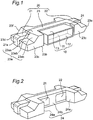
- FIG. 1 is a perspective view showing a configuration of the light emitting device of an embodiment of the present invention.
- FIG. 2 is a perspective view showing a configuration of a base member 20 with a first surface 23a as a mounting surface upward.
- the light emitting device can include the base member 20 having a recess 24, and a light emitting element 10 disposed on a bottom surface 24b of the recess in the base member 20.
- the base member 20 includes a resin-molded body 23, and a first lead 21 and a second lead 22 that are embedded in the resin-molded body 23.
- the resin-molded body 23 includes the first surface 23a which is one of two opposing main surfaces, a second surface 23b which is the other of the two opposing main surfaces, a front surface 23c, a rear surface 23f, a first end surface 23d, and a second end surface 23e, as well as the groove-shaped recess 24 in the front surface 23c.
- the first surface 23a as a mounting surface is shown upside. Accordingly, in a mounted state, the first surface 23a corresponds to a lower surface and the second surface 23b corresponds to an upper surface.
- the recess 24 is formed in the front surface 23c across the front surface 23c so as to penetrate from the first surface 23a to the second surface 23b, and includes the bottom surface 24b of the recess and two side walls 24a.
- the side walls 24a of the recess are preferably inclined such that an opening side of the recess is greater than the recess bottom surface 24b. Mounting of the light emitting element may be facilitated by making the opening side greater.
- the first surface 23a includes a stepped portion on each of a side of the first end surface 23d and a side of the second end surface 23e, and the resin-molded body 23 becomes thin at the stepped portion.
- a part excluding inclined surfaces 23ac and flat surfaces 23ab that are continuous from the corresponding inclined surfaces 23ac that constitute the stepped portions on the side of the first end surface 23d and the side of the second end surface 23e is referred to as a mount surface 23as.
- Examples of a material for molding the resin-molded body 23 can include a thermoplastic resin and a thermosetting resin, and more specifically, resins such as polyphthalamide (PPA), a polycarbonate resin, polyphenylenesulfide (PPS), liquid crystal polymer (LCP), an ABS resin, an epoxy resin, a phenolic resin, an acrylic resin, and a PBT resin. Further, it is possible to improve reflectance of light on the surface of the resin-molded body by mixing a light-reflective material such as titanium oxide into the material for molding. With this, it is possible to cause returning light to be efficiently reflected.
- resins such as polyphthalamide (PPA), a polycarbonate resin, polyphenylenesulfide (PPS), liquid crystal polymer (LCP), an ABS resin, an epoxy resin, a phenolic resin, an acrylic resin, and a PBT resin.
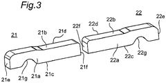
- the first lead 21 includes one end surface 21e and the other end surface 21f.
- the first lead 21 is formed in a pillar shape of a substantial hexahedron elongated in a direction from the one end surface 21e to the other end surface 21f.
- the first lead 21 includes four side surfaces 21a, 21b, 21c, and 21d between the one end surface 21e and the other end surface 21f.
- FIG. 3 shows the first lead 21 and the second lead 22 with their positional relation within the resin-molded body 23 maintained.
- the first lead 21 is embedded in the resin-molded body 23 such that the one end surface 21e is exposed at a central portion of the first end surface 23d of the resin-molded body 23, and a part of the side surface 21b on a side of the one end surface 21e is exposed from the inclined surface 23ac and the flat surface 23ab of the first surface 23a of the resin-molded body 23. A part of the side surface 21a of the first lead 21 on a side of the other end surface 21f is exposed at the bottom surface 24b of the recess of the resin-molded body 23.
- a recess 21g is provided in the side surface 21c of the first lead 21, and the recess prevents the first lead 21 from falling out of the resin-molded body 23.
- the second lead 22 includes one end surface 22e and the other end surface 22f.
- the second lead 22 is formed in a pillar shape of substantial hexahedron elongated in a direction from the one end surface 22e to the other end surface 22f.
- the second lead 22 includes four side surfaces 22a, 22b, 22c, and 22d between the one end surface 22e and the other end surface 22f.
- the second lead 22 is embedded in the resin-molded body 23 such that the one end surface 22e is exposed at a central portion of the second end surface 23e of the resin-molded body 23, and a part of the side surface 22b on a side of the one end surface 22e is exposed from the inclined surface 23ac and the flat surface 23ab of the first surface 23a of the resin-molded body 23.
- a part of the side surface 22a of the second lead 22 on a side of the other end surface 22f is exposed at the bottom surface 24b of the recess of the resin-molded body 23.
- a recess 22g is provided in the side surface 22c of the second lead 22, and the recess prevents the second lead 22 from falling out of the resin-molded body 23.
- the first lead 21 is embedded in the resin-molded body 23 such that the part of the side surface 21b on the side of the one end surface 21e is exposed from the resin-molded body 23, and the second lead 22 is embedded in the resin-molded body 23 such that the part of the side surface 22b on the side of the one end surface 22e is exposed from the resin-molded body 23.
- the present invention is not limited to such an example, and the first lead 21 and the second lead 22 may be embedded in the resin-molded body 23 such that, for example, the side surface 21b on the side of the other end surface 21f and the side surface 22b on the side of the other end surface 22f are exposed while positioned in the same plane as the mount surface 23as.
- first lead 21 and the second lead 22 may be embedded in the resin-molded body 23 such that the side surface 21b on the side of the other end surface 21f and the side surface 22b on the side of the other end surface 22f are exposed while extending from the mount surface 23as.
- each of the first lead 21 and the second lead 22 is formed in a pillar shape of substantial hexahedron elongated in one direction.
- the part of the side surface 21a on the side of the other end surface 21f is exposed at the bottom surface 24b of the recess, and the part on the side of the one end surface 21e of the side surface 21b that is perpendicular to the side surface 21a is constituted as a main external connection surface for connecting to an external circuit.
- the part of the side surface 22a on the side of the other end surface 22f is exposed at the bottom surface 24b of the recess, and the part on the side of the one end surface 22e of the side surface 22b that is perpendicular to the side surface 22a is constituted as a main external connection surface for connecting to an external circuit.
- each of the first lead 21 and the second lead 22 in a pillar shape of substantial hexahedron, it is possible to use one of the two side surfaces that are perpendicular to each other for connection with the light emitting element 10, and the other of the two side surfaces as the external connection surface, and thus to improve heat radiation characteristics.
- the first lead and the second lead may be made of a conductive material including at least one of aluminum, iron, nickel, copper, a copper alloy, stainless steel, and a ferro-alloy including Invar alloy, for example.
- a clad material having a cladding of different types of metals may also be used.
- a thickness of the lead frame is, for example, from 50 ⁇ m to 1000 ⁇ m, and preferably, from 100 ⁇ m to 500 ⁇ m.
- the thickness of the lead frame may be changed depending on the purpose. It is possible to change the thickness of the lead frame by etching (half etching) or press working.
- the base member 20 thus configured may be manufactured in the following manner, for example.
- a mold having a cavity corresponding to the shape of the resin-molded body 23 is prepared. Then, two columnar leads that are to be the first lead 21 and the second lead 22 are positioned in the cavity and fixed at a predetermined distance between their ends. The ends of the columnar leads positioned at the predetermined distance respectively correspond to the other end surface 21f and the other end surface 22f illustrated in FIG. 3 .
- the mold is configured by two or more molds that are separable, and one of the molds includes a projection corresponding to the recess 24, and the other of the molds includes a gate for injecting a resin.
- the resin-molded body After hardening the resin, the resin-molded body is taken out of the mold, and the columnar leads that extend outside the resin-molded body 23 are cut.
- the columnar first lead 21 and the columnar second lead 22 are cut along the first end surface 23d and the second end surface 23e (parallelly) such that the ends on the side of the one end surface 21e and the one end surface 22e project from the resin-molded body 23 by a predetermined length.
- the one end surfaces 21e and 22e respectively constituted by cutting surfaces are provided.
- the one end surface 21e constituted by the cutting surface is preferably perpendicular to the four side surfaces 21a, 21b, 21c, and 21d
- the one end surface 22e constituted by the cutting surface is preferably perpendicular to the four side surfaces 22a, 22b, 22c, and 22d.
- a portion represented by 28 is a gate trace of the resin-molded body 23.
- the base member 20 thus configured is provided with the recess 24 housing the light emitting element so as to penetrate from the first surface 23a to the second surface 23b, and its thickness (a distance between the first surface 23a and the second surface 23b) may be thin as there is no walls on the side of the first surface 23a and on the side of the second surface 23b (hereinafter, referred to as upper and lower walls).
- the recess 24 has no upper and lower walls, light from the light emitting element may leak from the side of the first surface 23a and the side of the second surface 23b, and it is not possible to efficiently extract light emitted from the light emitting element to a front side.
- embodiments of the present invention realize a thin light emitting device capable of efficiently extracting light from the light emitting element to the front side, by using a light emitting element having a reflecting layer provided on the side surfaces.
- Examples of the light emitting element 10 can include a light emitting element chip 11, a light transmissive member 12 disposed on a light-emitting surface of the light emitting element chip 11, and a reflecting layer 13 covering an periphery of the light emitting element chip 11 and an periphery of the light transmissive member 12.
- the light emitting element 10 can be configured such that a side surface of a quadrangular prismatic body defined by a chip mounting surface of the light emitting element chip 11 on which a positive electrode 3a and a negative electrode 3b are provided, an upper surface of the light transmissive member 12, and side surfaces that are perpendicular to the upper surface and the chip mounting surface are covered by the reflecting layer 13, and an outer shape of the light emitting element 10 including the reflecting layer 13 is also in a quadrangular prismatic body.
- the quadrangular prismatic body excluding the reflecting layer 13 is referred to as an inner quadrangular prismatic body
- the quadrangular prismatic body including the reflecting layer 13 is referred to as an outer quadrangular prismatic body.
- the shape of the light emitting element 10 is not limited to quadrangular prismatic body, but manufacturing of the light emitting element 10 is facilitated when the shape of the light emitting element 10 is a quadrangular prismatic body.
- manufacturing of the light emitting element 10 is facilitated when the shape of the light emitting element 10 is a quadrangular prismatic body.
- the light emitting element chip 11 having the positive electrode 3a and the negative electrode 3b on the same surface is prepared.
- the light emitting element chip 11 may be any light emitting element as long as a light-emitting layer made of semiconductor is provided.
- a light emitting element having a light-emitting layer made of nitride semiconductor, especially gallium nitride-based compound semiconductor (particularly InGaN) may be suitably combined with a phosphor, as this type of light emitting element is able to emit intense light in a short wavelength region and a near-ultraviolet region in a visual light range.
- a light emission peak wavelength of outgoing light emitted from light-emitting layer of the light emitting element chip 11 has a light emission spectrum around 240 nm to 500 nm which is in the short wavelength region from the near-ultraviolet light to visible light, preferably 380 nm to 420 nm, and more preferably 450 nm to 470 nm.
- a light emitting element emitting light in this wavelength region is able to emit light of a desired color, in particular white light, in combination with a phosphor of various types.
- the light emitting element 10 may have a light-emitting layer made of such as ZnSe-based, InGaAs-based, or AlInGaP-based semiconductor.
- the light transmissive member 12 provided with a light transmissive substrate 1 and a wavelength conversion layer 2 disposed on one surface of the light transmissive substrate 1 is prepared.
- a wavelength conversion member is disposed on the light transmissive substrate, and cut into the same size as the light emitting element chip 11, for example.
- Examples of the light transmissive substrate 1 include glass substrates made of quartz and borosilicate glass.
- a thickness of the light transmissive substrate 1 is preferably from 30 ⁇ m to 1 mm, and more preferably from 50 ⁇ m to 500 ⁇ m.
- a binder resin mixed with a phosphor described later may be used as the wavelength conversion layer 2.
- the phosphor is selected from phosphors excited by light emitted from the light emitting element chip 11. If, for example, the light emitting element chip 11 is a blue light emitting element and it is desired to configure a white light emitting device, it is preferable to use a phosphor that is excited by blue light and exhibits yellow broad light emission.
- a phosphor include phosphors having a cerium-activated garnet structure (in particular, a phosphor activated by cerium, containing aluminum, and having a garnet structure). As a cerium-activated phosphor exhibits yellow broad light emission, it is possible to realize white light with favorable color rendering properties in combination with blue light emission.
- a phosphor having a garnet structure in particular, a phosphor containing aluminum and having a garnet structure is resistant to heat, light, and moisture, and is able to maintain yellow light emission at high brightness for an extended period of time.
- a YAG-based phosphor (generally abbreviated to YAG) expressed by (Re 1-x Sm x ) 3 (A 1-y Ga y ) 5 O 12 :Ce (0 ⁇ x ⁇ 1, 0 ⁇ y ⁇ 1, where Re is at least one of elements selected from a group consisting of Y, Gd, La, Lu, and Tb).
- a phosphor such as Si 6-Z Al Z O Z N 8-Z :Eu, Lu 3 Al 5 O 12 :Ce, BaMgAl 10 O 17 :Eu, BaMgAl 10 O 17 :Eu, Mn, (Zn, Cd)Zn:Cu, (Sr, Ca) 10 (PO 4 ) 6 C 12 :Eu, Mn, (Sr, Ca) 2 Si 5 N 8 :Eu, CaAlSiB x N 3+x :Eu, K 2 SiF 6 :Mn, or CaAlSiN 3 :Eu is used to adjust color rendering properties of a light source for lighting and color reproducibility in use of backlight.
- a quantum dot phosphor may also be used.
- the wavelength conversion layer 2 may include more than two types of phosphors.
- a first type of the phosphors may be excited by primary light from the light emitting element chip 11 to emit light, and a second type of the phosphors may be excited by secondary light emitted from the first type of the phosphors to emit light.
- two types of phosphors of different chromaticity are used, by adjusting amounts of the two types of phosphors, it is possible to achieve light emission corresponding to an arbitrary chromaticity point within a region defined by connecting chromaticity point of each of the two types of phosphors and the light emitting element on a chromaticity diagram.
- a silicone resin or a modified silicone resin can be used as the binder resin.
- an insulating resin having light transmissivity such as an epoxy resin, a modified epoxy resin, or an acrylic resin may be used.
- a resin having a superior weather resistance such as a hybrid resin including at least one of these resins may also be used.
- Examples of a method of providing the wavelength conversion layer 2 include known methods such as printing, spray coating, compression molding, spin coat, and dispensing.
- the wavelength conversion layer 2 be provided such that a film thickness is uniform and phosphor particles may not be eccentrically located.
- light emitting element chips 11 are arranged on a sheet 6 in matrix at predetermined intervals with a surface having the positive electrode 3a and the negative electrode 3b downside.
- the predetermined intervals at which the light emitting element chips 11 are arranged are set considering a thickness t of the reflecting layer 13. Specifically, the intervals are set to a value obtained by adding a value that is twice as large as the thickness t of the reflecting layer 13 with a cutting width that will be later described.
- the sheet 6 is provided with an adhesive layer or a sticking layer, for example, on one surface, and the light emitting element chips 11 are maintained at the predetermined intervals by the adhesive layer or the sticking layer.
- the light transmissive member 12 having the wavelength conversion layer 2 is joined onto each of the light emitting element chips 11 by an adhesive member 4.
- the light transmissive substrate 1 is manufactured in a planar shape of a size that is the same as or slightly larger than the light emitting element chip 11, and the wavelength conversion layer 2 is joined to the light emitting element chip 11 via the adhesive member 4 made for example of a silicone resin.
- the adhesive member 4 made for example of a silicone resin.
- a resin 5 constituting the reflecting layer 13 is applied such that the resin 5 is filled between the arranged inner quadrangular columnar bodies.
- a light-reflective material is contained in the resin 5. With this, it is possible to improve light emission efficiency by reflecting light emitted from the side surfaces of the light emitting element chip 11 by the light-reflective material contained in the resin 5 toward the wavelength conversion layer 2. At least one selected from a group constituting of TiO 2 , ZrO 2 , Nb 2 O 5 , Al 2 O 3 , MgF, AlN, SiO 2 , and MgO may be used as the light-reflective material.
- the resin 5 containing the light-reflective material is filled between the arranged light emitting elements chip 11 by applying the resin 5 and spreading the resin 5 using a squeegee.
- the squeegee is moved along the upper surface of the light transmissive substrate 1 of the light transmissive member 12, and causes the resin 5 to fill between the light emitting element chips 11 such that the upper surface of the resin 5 and the upper surface of the light transmissive substrate 1 are positioned in the substantially same plane.
- the hardened resin 5 is cut along a cutting line 7 by dicing, for example, into individual light emitting elements.
- the cutting line 7 is set so as to match a center line between adjacent light emitting element chips 11, for example.
- a distance between the cutting line 7 and the side surface of the light emitting element chip 11 is set such that the thickness t of the reflecting layer 13 after the cutting is a predetermined thickness.
- the light emitting element 10 including the light emitting element chip 11, the light transmissive member 12 disposed on the light-emitting surface of the light emitting element chip 11, the reflecting layer 13 covering the periphery of the light emitting element chip 11 and the light transmissive member 12 is manufactured.
- a leakage of light through the side surface of the inner quadrangular prismatic body is prevented by providing the reflecting layer 13 on or over an entire side surface of the inner quadrangular prismatic body.
- the reflecting layer may be provided on or over a part of the side surface of the inner quadrangular prismatic body to restrict the light-emitting region to a predetermined range.
- the resin 5 constituting the reflecting layer 13 may be provided between the arranged inner quadrangular columnar bodies to a predetermined depth, and then the reflecting layer may be provided on or over a part of the side surface of the inner quadrangular prismatic body.
- the reflecting layer 13 it is possible to appropriately set a region in which the reflecting layer 13 is provided on the side surface of the inner quadrangular prismatic body based on a required light extracting efficiency, the shape of the package recess, and required directional characteristics.
- the light emitting element 10 thus manufactured is mounted on the recess bottom surface 24b of the base member 20 by flip-chip mounting, and thus the light emitting device according to an embodiment of the present invention is completed.
- the example in which the light transmissive member 12 is configured by the light transmissive substrate 1 and the wavelength conversion layer 2 provided on one surface of the light transmissive substrate 1 has been described.
- the present invention is not limited to such an example.
- the light emitting element 10 may be configured by providing the wavelength conversion layer on or over the light emitting element chip 11, and providing the transparent resin layer on or over the wavelength conversion layer.
- the light transmissive member 12 may be configured by a single resin layer containing the phosphor, or by a single resin layer containing no phosphor.
- the light transmissive member 12 may be configured by a plurality of resin layers including or not including the wavelength conversion layer 2.
- the recess 24 housing the light emitting element 10 is provided so as to penetrate from the first surface 23a to the second surface 23b in the base member 20, and there are no upper and lower walls on the sides of the first surface 23a and the second surface 23b. Therefore, the light emitting device according to an embodiment of the present invention may be made thin.
- the reflecting layer 13 is provided on or over the side surface of the light emitting element 10, it is possible to efficiently extract light from the light emitting element to the front side.
- the light emitting device has no upper and lower walls in the recess 24, it is possible to increase a ratio of a volume of the light emitting element 10 in the recess 24, and to make its size smaller and thinner.
- the recess has upper and lower walls, it is necessary to provide a gap above a predetermined level between the upper and lower walls and the light emitting elements in order to facilitate mounting of the light emitting element, the present invention does not require such an extra space for mounting.
- the upper and lower walls is required to be inclined in order to cause light from the light emitting element to be efficiently reflected to a front side in the configuration in which the reflecting layer is provided for the upper and lower walls.
- the reflecting layer 13 is provided integrally with the light emitting element 10 spaced apart from the side walls of the recess, and therefore it is possible to restrict the light-emitting region to a narrower region, and effectively to a predetermined range.
- the expression that the reflecting layer 13 is spaced apart from the side walls of the recess means that there is a distance between the reflecting layer 13 and the side walls of the recess as compared to the case in which the reflecting layer is provided for the side walls of the recess, and a part of the reflecting layer may be in contact with the side walls of the recess, for example.
- the light emitting device is able to restrict the light-emitting region to a desired region by appropriately setting a region in which the reflecting layer 13 is provided.
- the first surface 23a includes the stepped portion on each of the side of the first end surface 23d and the side of the second end surface 23e, and a reservoir for a bonding member (such as soldering) is provided on each of the sides of the first lead 21 and the second lead 22 exposed from the resin-molded body 23.
- a bonding member such as soldering
- the light emitting device improves the heat radiation characteristics using the columnar-shaped first lead 21 and the columnar-shaped second lead 22. Specifically, if the first lead and the second lead are configured using metal flakes as in the conventional technique, the heat radiation characteristics deteriorate as the first lead and the second lead become smaller and thinner.
- the light emitting device improves the heat radiation characteristics by increasing a ratio of metallic components that constitute the first lead 21 and the second lead 22 in the resin-molded body 23 using the columnar-shaped first lead 21 and the columnar-shaped second lead 22. It is preferable that the ratio of the metallic components that constitute the first lead 21 and the second lead 22 in the resin-molded body 23 is as high as possible. This is because both the heat radiation characteristics and facility for implementation are improved as the ratio of the leads increases.
- the first surface 23a includes the stepped portion on each of the side of the first end surface 23d and the side of the second end surface 23e, and an area of the first lead 21 and the second lead 22 exposed from the resin-molded body 23 on the side of the first end surface 23d and on the side of the second end surface 23e is increased. With this, it is possible to more effectively radiate heat in an actual implementation.
- the present disclosure includes the following aspects:
Landscapes
- Led Device Packages (AREA)
Applications Claiming Priority (1)
| Application Number | Priority Date | Filing Date | Title |
|---|---|---|---|
| JP2013177773A JP6236999B2 (ja) | 2013-08-29 | 2013-08-29 | 発光装置 |
Publications (2)
| Publication Number | Publication Date |
|---|---|
| EP2843718A1 EP2843718A1 (en) | 2015-03-04 |
| EP2843718B1 true EP2843718B1 (en) | 2017-11-29 |
Family
ID=51417185
Family Applications (1)
| Application Number | Title | Priority Date | Filing Date |
|---|---|---|---|
| EP14182481.3A Active EP2843718B1 (en) | 2013-08-29 | 2014-08-27 | Light emitting device |
Country Status (6)
| Country | Link |
|---|---|
| US (2) | US10109779B2 (enExample) |
| EP (1) | EP2843718B1 (enExample) |
| JP (1) | JP6236999B2 (enExample) |
| KR (1) | KR102161069B1 (enExample) |
| CN (1) | CN104425701B (enExample) |
| TW (1) | TWI680592B (enExample) |
Families Citing this family (6)
| Publication number | Priority date | Publication date | Assignee | Title |
|---|---|---|---|---|
| CN106206912B (zh) * | 2015-05-29 | 2020-08-07 | 日亚化学工业株式会社 | 发光装置、覆盖部件的制造方法及发光装置的制造方法 |
| KR102674066B1 (ko) * | 2016-11-11 | 2024-06-13 | 삼성전자주식회사 | 발광 소자 패키지 |
| KR102406913B1 (ko) * | 2017-03-27 | 2022-06-10 | 서울반도체 주식회사 | 발광 모듈 |
| DE102017116279B4 (de) * | 2017-07-19 | 2023-08-03 | OSRAM Opto Semiconductors Gesellschaft mit beschränkter Haftung | Verfahren zur Herstellung einer Vielzahl von Konversionselementen und optoelektronisches Bauelement |
| CN112490224B (zh) * | 2020-11-27 | 2025-04-08 | 广东晶科电子股份有限公司 | 一种发光装置及制作方法 |
| TWI821731B (zh) * | 2021-08-23 | 2023-11-11 | 啟端光電股份有限公司 | 底部發光型發光二極體顯示器 |
Citations (1)
| Publication number | Priority date | Publication date | Assignee | Title |
|---|---|---|---|---|
| EP2315263A1 (en) * | 2008-07-29 | 2011-04-27 | Nichia Corporation | Light-emitting device |
Family Cites Families (31)
| Publication number | Priority date | Publication date | Assignee | Title |
|---|---|---|---|---|
| TWI292961B (en) * | 2002-09-05 | 2008-01-21 | Nichia Corp | Semiconductor device and an optical device using the semiconductor device |
| DE102004021233A1 (de) | 2004-04-30 | 2005-12-01 | Osram Opto Semiconductors Gmbh | Leuchtdiodenanordnung |
| JP2006269448A (ja) * | 2005-03-22 | 2006-10-05 | Stanley Electric Co Ltd | Led |
| WO2006111906A2 (en) * | 2005-04-19 | 2006-10-26 | Philips Intellectual Property & Standards Gmbh | Illumination system comprising a red-emitting ceramic luminescence converter |
| TWI302041B (en) * | 2006-01-19 | 2008-10-11 | Everlight Electronics Co Ltd | Light emitting diode packaging structure |
| JP4857791B2 (ja) * | 2006-02-01 | 2012-01-18 | 日亜化学工業株式会社 | 半導体装置の製造方法 |
| TWI331815B (en) * | 2006-03-17 | 2010-10-11 | Seoul Semiconductor Co Ltd | Side-view light emitting diode package having a reflector |
| JP4952215B2 (ja) * | 2006-08-17 | 2012-06-13 | 日亜化学工業株式会社 | 発光装置 |
| JP5205773B2 (ja) | 2006-11-07 | 2013-06-05 | 日亜化学工業株式会社 | 発光装置 |
| JP2008187030A (ja) * | 2007-01-30 | 2008-08-14 | Stanley Electric Co Ltd | 発光装置 |
| JP5132961B2 (ja) * | 2007-03-19 | 2013-01-30 | ハリソン東芝ライティング株式会社 | 光半導体装置及びその製造方法 |
| KR101374895B1 (ko) * | 2007-03-31 | 2014-03-17 | 서울반도체 주식회사 | 측면 발광형 led 패키지 및 그 제조방법 |
| JP2009032746A (ja) * | 2007-07-24 | 2009-02-12 | Harison Toshiba Lighting Corp | 発光装置及び発光ユニット |
| JP2009038184A (ja) * | 2007-08-01 | 2009-02-19 | Harison Toshiba Lighting Corp | 半導体発光装置、光源装置及び面状発光装置 |
| US8360593B2 (en) * | 2007-09-28 | 2013-01-29 | Seoul Semiconductor Co., Ltd. | LED package and back light unit using the same |
| JP5277610B2 (ja) * | 2007-10-29 | 2013-08-28 | 日亜化学工業株式会社 | 発光装置及び面発光装置並びに発光装置用パッケージ |
| WO2009075530A2 (en) | 2007-12-13 | 2009-06-18 | Amoleds Co., Ltd. | Semiconductor and manufacturing method thereof |
| WO2009093427A1 (ja) * | 2008-01-21 | 2009-07-30 | Nichia Corporation | 発光装置 |
| JP2010003743A (ja) * | 2008-06-18 | 2010-01-07 | Toshiba Corp | 発光装置 |
| KR101537797B1 (ko) * | 2008-06-26 | 2015-07-22 | 서울반도체 주식회사 | 발광장치 |
| JP5294741B2 (ja) | 2008-07-14 | 2013-09-18 | 日亜化学工業株式会社 | 樹脂成形体及び表面実装型発光装置並びにそれらの製造方法 |
| DE102008049399B4 (de) * | 2008-09-29 | 2021-09-02 | OSRAM Opto Semiconductors Gesellschaft mit beschränkter Haftung | Optoelektronisches Bauelement, optoelektronische Vorrichtung und Verfahren zur Herstellung eines optoelektronischen Bauelements |
| JP4808244B2 (ja) | 2008-12-09 | 2011-11-02 | スタンレー電気株式会社 | 半導体発光装置およびその製造方法 |
| US8097894B2 (en) | 2009-07-23 | 2012-01-17 | Koninklijke Philips Electronics N.V. | LED with molded reflective sidewall coating |
| JP5496570B2 (ja) | 2009-08-05 | 2014-05-21 | シャープ株式会社 | 発光装置 |
| JP5251788B2 (ja) * | 2009-08-25 | 2013-07-31 | 豊田合成株式会社 | サイドビュータイプの発光装置及びその製造方法 |
| JP5482098B2 (ja) * | 2009-10-26 | 2014-04-23 | 日亜化学工業株式会社 | 発光装置 |
| US8581287B2 (en) | 2011-01-24 | 2013-11-12 | Stanley Electric Co., Ltd. | Semiconductor light emitting device having a reflective material, wavelength converting layer and optical plate with rough and plane surface regions, and method of manufacturing |
| JP5744643B2 (ja) | 2011-06-28 | 2015-07-08 | シチズン電子株式会社 | 発光装置の製造方法 |
| JP2013077679A (ja) | 2011-09-30 | 2013-04-25 | Citizen Electronics Co Ltd | 半導体発光装置とその製造方法 |
| WO2014014298A1 (ko) * | 2012-07-18 | 2014-01-23 | 주식회사 세미콘라이트 | 반도체 발광소자의 제조 방법 |
-
2013
- 2013-08-29 JP JP2013177773A patent/JP6236999B2/ja active Active
-
2014
- 2014-08-08 TW TW103127339A patent/TWI680592B/zh active
- 2014-08-22 KR KR1020140109369A patent/KR102161069B1/ko active Active
- 2014-08-26 CN CN201410424943.7A patent/CN104425701B/zh active Active
- 2014-08-26 US US14/468,755 patent/US10109779B2/en active Active
- 2014-08-27 EP EP14182481.3A patent/EP2843718B1/en active Active
-
2018
- 2018-09-21 US US16/138,536 patent/US10622529B2/en active Active
Patent Citations (1)
| Publication number | Priority date | Publication date | Assignee | Title |
|---|---|---|---|---|
| EP2315263A1 (en) * | 2008-07-29 | 2011-04-27 | Nichia Corporation | Light-emitting device |
Also Published As
| Publication number | Publication date |
|---|---|
| JP6236999B2 (ja) | 2017-11-29 |
| KR102161069B1 (ko) | 2020-09-29 |
| CN104425701B (zh) | 2019-06-18 |
| CN104425701A (zh) | 2015-03-18 |
| KR20150026858A (ko) | 2015-03-11 |
| EP2843718A1 (en) | 2015-03-04 |
| TWI680592B (zh) | 2019-12-21 |
| US10109779B2 (en) | 2018-10-23 |
| TW201513406A (zh) | 2015-04-01 |
| US10622529B2 (en) | 2020-04-14 |
| US20190027663A1 (en) | 2019-01-24 |
| US20150060921A1 (en) | 2015-03-05 |
| JP2015046534A (ja) | 2015-03-12 |
Similar Documents
| Publication | Publication Date | Title |
|---|---|---|
| US10622529B2 (en) | Light emitting device | |
| JP5217800B2 (ja) | 発光装置、樹脂パッケージ、樹脂成形体並びにこれらの製造方法 | |
| KR100625720B1 (ko) | 반도체 장치 및 그것을 이용한 광학 장치 | |
| JP5766976B2 (ja) | 発光装置の製造方法 | |
| JP2016154255A (ja) | 発光装置 | |
| JP2017107965A (ja) | パッケージの製造方法及び発光装置の製造方法、並びにパッケージ及び発光装置 | |
| JP5900586B2 (ja) | 発光装置 | |
| TWI593133B (zh) | 封裝之製造方法及發光裝置之製造方法、與封裝及發光裝置 | |
| JP6056934B2 (ja) | 発光装置、樹脂パッケージ、樹脂成形体並びにこれらの製造方法 | |
| JP5527450B2 (ja) | 発光装置、樹脂パッケージ、樹脂成形体並びにこれらの製造方法 | |
| JP6164355B2 (ja) | 発光装置、樹脂パッケージ、樹脂成形体並びにこれらの製造方法 | |
| JP2013145908A (ja) | 発光装置、樹脂パッケージ、樹脂成形体並びにこれらの製造方法 | |
| JP5825390B2 (ja) | 発光装置、樹脂パッケージ、樹脂成形体並びにこれらの製造方法 | |
| JP2018121084A (ja) | 発光装置の製造方法及び発光装置 | |
| JP6489162B2 (ja) | 樹脂成形体付リードフレーム及びこれの製造方法並びにこれらに用いるリードフレーム |
Legal Events
| Date | Code | Title | Description |
|---|---|---|---|
| 17P | Request for examination filed |
Effective date: 20140827 |
|
| AK | Designated contracting states |
Kind code of ref document: A1 Designated state(s): AL AT BE BG CH CY CZ DE DK EE ES FI FR GB GR HR HU IE IS IT LI LT LU LV MC MK MT NL NO PL PT RO RS SE SI SK SM TR |
|
| AX | Request for extension of the european patent |
Extension state: BA ME |
|
| PUAI | Public reference made under article 153(3) epc to a published international application that has entered the european phase |
Free format text: ORIGINAL CODE: 0009012 |
|
| R17P | Request for examination filed (corrected) |
Effective date: 20150901 |
|
| RBV | Designated contracting states (corrected) |
Designated state(s): AL AT BE BG CH CY CZ DE DK EE ES FI FR GB GR HR HU IE IS IT LI LT LU LV MC MK MT NL NO PL PT RO RS SE SI SK SM TR |
|
| 17Q | First examination report despatched |
Effective date: 20161010 |
|
| GRAP | Despatch of communication of intention to grant a patent |
Free format text: ORIGINAL CODE: EPIDOSNIGR1 |
|
| RIC1 | Information provided on ipc code assigned before grant |
Ipc: H01L 33/60 20100101AFI20170316BHEP Ipc: H01L 33/62 20100101ALN20170316BHEP Ipc: H01L 33/48 20100101ALN20170316BHEP Ipc: H01L 23/00 20060101ALN20170316BHEP |
|
| RIC1 | Information provided on ipc code assigned before grant |
Ipc: H01L 33/60 20100101AFI20170322BHEP Ipc: H01L 23/00 20060101ALN20170322BHEP Ipc: H01L 33/62 20100101ALN20170322BHEP Ipc: H01L 33/48 20100101ALN20170322BHEP |
|
| INTG | Intention to grant announced |
Effective date: 20170411 |
|
| GRAS | Grant fee paid |
Free format text: ORIGINAL CODE: EPIDOSNIGR3 |
|
| GRAJ | Information related to disapproval of communication of intention to grant by the applicant or resumption of examination proceedings by the epo deleted |
Free format text: ORIGINAL CODE: EPIDOSDIGR1 |
|
| GRAL | Information related to payment of fee for publishing/printing deleted |
Free format text: ORIGINAL CODE: EPIDOSDIGR3 |
|
| GRAR | Information related to intention to grant a patent recorded |
Free format text: ORIGINAL CODE: EPIDOSNIGR71 |
|
| RIN1 | Information on inventor provided before grant (corrected) |
Inventor name: OKAHISA, TSUYOSHI |
|
| INTC | Intention to grant announced (deleted) | ||
| RIC1 | Information provided on ipc code assigned before grant |
Ipc: H01L 33/62 20100101ALN20170918BHEP Ipc: H01L 33/48 20100101ALN20170918BHEP Ipc: H01L 23/00 20060101ALN20170918BHEP Ipc: H01L 33/60 20100101AFI20170918BHEP |
|
| GRAA | (expected) grant |
Free format text: ORIGINAL CODE: 0009210 |
|
| INTG | Intention to grant announced |
Effective date: 20170925 |
|
| AK | Designated contracting states |
Kind code of ref document: B1 Designated state(s): AL AT BE BG CH CY CZ DE DK EE ES FI FR GB GR HR HU IE IS IT LI LT LU LV MC MK MT NL NO PL PT RO RS SE SI SK SM TR |
|
| REG | Reference to a national code |
Ref country code: CH Ref legal event code: EP |
|
| REG | Reference to a national code |
Ref country code: AT Ref legal event code: REF Ref document number: 951140 Country of ref document: AT Kind code of ref document: T Effective date: 20171215 |
|
| REG | Reference to a national code |
Ref country code: IE Ref legal event code: FG4D |
|
| REG | Reference to a national code |
Ref country code: DE Ref legal event code: R096 Ref document number: 602014017806 Country of ref document: DE |
|
| REG | Reference to a national code |
Ref country code: NL Ref legal event code: MP Effective date: 20171129 |
|
| REG | Reference to a national code |
Ref country code: LT Ref legal event code: MG4D |
|
| REG | Reference to a national code |
Ref country code: AT Ref legal event code: MK05 Ref document number: 951140 Country of ref document: AT Kind code of ref document: T Effective date: 20171129 |
|
| PG25 | Lapsed in a contracting state [announced via postgrant information from national office to epo] |
Ref country code: ES Free format text: LAPSE BECAUSE OF FAILURE TO SUBMIT A TRANSLATION OF THE DESCRIPTION OR TO PAY THE FEE WITHIN THE PRESCRIBED TIME-LIMIT Effective date: 20171129 Ref country code: FI Free format text: LAPSE BECAUSE OF FAILURE TO SUBMIT A TRANSLATION OF THE DESCRIPTION OR TO PAY THE FEE WITHIN THE PRESCRIBED TIME-LIMIT Effective date: 20171129 Ref country code: NO Free format text: LAPSE BECAUSE OF FAILURE TO SUBMIT A TRANSLATION OF THE DESCRIPTION OR TO PAY THE FEE WITHIN THE PRESCRIBED TIME-LIMIT Effective date: 20180228 Ref country code: SE Free format text: LAPSE BECAUSE OF FAILURE TO SUBMIT A TRANSLATION OF THE DESCRIPTION OR TO PAY THE FEE WITHIN THE PRESCRIBED TIME-LIMIT Effective date: 20171129 Ref country code: LT Free format text: LAPSE BECAUSE OF FAILURE TO SUBMIT A TRANSLATION OF THE DESCRIPTION OR TO PAY THE FEE WITHIN THE PRESCRIBED TIME-LIMIT Effective date: 20171129 |
|
| PG25 | Lapsed in a contracting state [announced via postgrant information from national office to epo] |
Ref country code: BG Free format text: LAPSE BECAUSE OF FAILURE TO SUBMIT A TRANSLATION OF THE DESCRIPTION OR TO PAY THE FEE WITHIN THE PRESCRIBED TIME-LIMIT Effective date: 20180228 Ref country code: RS Free format text: LAPSE BECAUSE OF FAILURE TO SUBMIT A TRANSLATION OF THE DESCRIPTION OR TO PAY THE FEE WITHIN THE PRESCRIBED TIME-LIMIT Effective date: 20171129 Ref country code: LV Free format text: LAPSE BECAUSE OF FAILURE TO SUBMIT A TRANSLATION OF THE DESCRIPTION OR TO PAY THE FEE WITHIN THE PRESCRIBED TIME-LIMIT Effective date: 20171129 Ref country code: GR Free format text: LAPSE BECAUSE OF FAILURE TO SUBMIT A TRANSLATION OF THE DESCRIPTION OR TO PAY THE FEE WITHIN THE PRESCRIBED TIME-LIMIT Effective date: 20180301 Ref country code: AT Free format text: LAPSE BECAUSE OF FAILURE TO SUBMIT A TRANSLATION OF THE DESCRIPTION OR TO PAY THE FEE WITHIN THE PRESCRIBED TIME-LIMIT Effective date: 20171129 Ref country code: HR Free format text: LAPSE BECAUSE OF FAILURE TO SUBMIT A TRANSLATION OF THE DESCRIPTION OR TO PAY THE FEE WITHIN THE PRESCRIBED TIME-LIMIT Effective date: 20171129 |
|
| PG25 | Lapsed in a contracting state [announced via postgrant information from national office to epo] |
Ref country code: NL Free format text: LAPSE BECAUSE OF FAILURE TO SUBMIT A TRANSLATION OF THE DESCRIPTION OR TO PAY THE FEE WITHIN THE PRESCRIBED TIME-LIMIT Effective date: 20171129 |
|
| REG | Reference to a national code |
Ref country code: FR Ref legal event code: PLFP Year of fee payment: 5 |
|
| PG25 | Lapsed in a contracting state [announced via postgrant information from national office to epo] |
Ref country code: CZ Free format text: LAPSE BECAUSE OF FAILURE TO SUBMIT A TRANSLATION OF THE DESCRIPTION OR TO PAY THE FEE WITHIN THE PRESCRIBED TIME-LIMIT Effective date: 20171129 Ref country code: SK Free format text: LAPSE BECAUSE OF FAILURE TO SUBMIT A TRANSLATION OF THE DESCRIPTION OR TO PAY THE FEE WITHIN THE PRESCRIBED TIME-LIMIT Effective date: 20171129 Ref country code: EE Free format text: LAPSE BECAUSE OF FAILURE TO SUBMIT A TRANSLATION OF THE DESCRIPTION OR TO PAY THE FEE WITHIN THE PRESCRIBED TIME-LIMIT Effective date: 20171129 Ref country code: CY Free format text: LAPSE BECAUSE OF FAILURE TO SUBMIT A TRANSLATION OF THE DESCRIPTION OR TO PAY THE FEE WITHIN THE PRESCRIBED TIME-LIMIT Effective date: 20171129 Ref country code: DK Free format text: LAPSE BECAUSE OF FAILURE TO SUBMIT A TRANSLATION OF THE DESCRIPTION OR TO PAY THE FEE WITHIN THE PRESCRIBED TIME-LIMIT Effective date: 20171129 |
|
| REG | Reference to a national code |
Ref country code: DE Ref legal event code: R097 Ref document number: 602014017806 Country of ref document: DE |
|
| PG25 | Lapsed in a contracting state [announced via postgrant information from national office to epo] |
Ref country code: RO Free format text: LAPSE BECAUSE OF FAILURE TO SUBMIT A TRANSLATION OF THE DESCRIPTION OR TO PAY THE FEE WITHIN THE PRESCRIBED TIME-LIMIT Effective date: 20171129 Ref country code: SM Free format text: LAPSE BECAUSE OF FAILURE TO SUBMIT A TRANSLATION OF THE DESCRIPTION OR TO PAY THE FEE WITHIN THE PRESCRIBED TIME-LIMIT Effective date: 20171129 Ref country code: PL Free format text: LAPSE BECAUSE OF FAILURE TO SUBMIT A TRANSLATION OF THE DESCRIPTION OR TO PAY THE FEE WITHIN THE PRESCRIBED TIME-LIMIT Effective date: 20171129 Ref country code: IT Free format text: LAPSE BECAUSE OF FAILURE TO SUBMIT A TRANSLATION OF THE DESCRIPTION OR TO PAY THE FEE WITHIN THE PRESCRIBED TIME-LIMIT Effective date: 20171129 |
|
| PLBE | No opposition filed within time limit |
Free format text: ORIGINAL CODE: 0009261 |
|
| STAA | Information on the status of an ep patent application or granted ep patent |
Free format text: STATUS: NO OPPOSITION FILED WITHIN TIME LIMIT |
|
| 26N | No opposition filed |
Effective date: 20180830 |
|
| PG25 | Lapsed in a contracting state [announced via postgrant information from national office to epo] |
Ref country code: SI Free format text: LAPSE BECAUSE OF FAILURE TO SUBMIT A TRANSLATION OF THE DESCRIPTION OR TO PAY THE FEE WITHIN THE PRESCRIBED TIME-LIMIT Effective date: 20171129 |
|
| PG25 | Lapsed in a contracting state [announced via postgrant information from national office to epo] |
Ref country code: MC Free format text: LAPSE BECAUSE OF FAILURE TO SUBMIT A TRANSLATION OF THE DESCRIPTION OR TO PAY THE FEE WITHIN THE PRESCRIBED TIME-LIMIT Effective date: 20171129 |
|
| REG | Reference to a national code |
Ref country code: CH Ref legal event code: PL |
|
| PG25 | Lapsed in a contracting state [announced via postgrant information from national office to epo] |
Ref country code: CH Free format text: LAPSE BECAUSE OF NON-PAYMENT OF DUE FEES Effective date: 20180831 Ref country code: LU Free format text: LAPSE BECAUSE OF NON-PAYMENT OF DUE FEES Effective date: 20180827 Ref country code: LI Free format text: LAPSE BECAUSE OF NON-PAYMENT OF DUE FEES Effective date: 20180831 |
|
| REG | Reference to a national code |
Ref country code: BE Ref legal event code: MM Effective date: 20180831 |
|
| PG25 | Lapsed in a contracting state [announced via postgrant information from national office to epo] |
Ref country code: BE Free format text: LAPSE BECAUSE OF NON-PAYMENT OF DUE FEES Effective date: 20180831 |
|
| PG25 | Lapsed in a contracting state [announced via postgrant information from national office to epo] |
Ref country code: MT Free format text: LAPSE BECAUSE OF NON-PAYMENT OF DUE FEES Effective date: 20180827 |
|
| PG25 | Lapsed in a contracting state [announced via postgrant information from national office to epo] |
Ref country code: TR Free format text: LAPSE BECAUSE OF FAILURE TO SUBMIT A TRANSLATION OF THE DESCRIPTION OR TO PAY THE FEE WITHIN THE PRESCRIBED TIME-LIMIT Effective date: 20171129 |
|
| PG25 | Lapsed in a contracting state [announced via postgrant information from national office to epo] |
Ref country code: HU Free format text: LAPSE BECAUSE OF FAILURE TO SUBMIT A TRANSLATION OF THE DESCRIPTION OR TO PAY THE FEE WITHIN THE PRESCRIBED TIME-LIMIT; INVALID AB INITIO Effective date: 20140827 Ref country code: PT Free format text: LAPSE BECAUSE OF FAILURE TO SUBMIT A TRANSLATION OF THE DESCRIPTION OR TO PAY THE FEE WITHIN THE PRESCRIBED TIME-LIMIT Effective date: 20171129 |
|
| PG25 | Lapsed in a contracting state [announced via postgrant information from national office to epo] |
Ref country code: IE Free format text: LAPSE BECAUSE OF NON-PAYMENT OF DUE FEES Effective date: 20180827 Ref country code: MK Free format text: LAPSE BECAUSE OF NON-PAYMENT OF DUE FEES Effective date: 20171129 |
|
| PG25 | Lapsed in a contracting state [announced via postgrant information from national office to epo] |
Ref country code: AL Free format text: LAPSE BECAUSE OF FAILURE TO SUBMIT A TRANSLATION OF THE DESCRIPTION OR TO PAY THE FEE WITHIN THE PRESCRIBED TIME-LIMIT Effective date: 20171129 Ref country code: IS Free format text: LAPSE BECAUSE OF FAILURE TO SUBMIT A TRANSLATION OF THE DESCRIPTION OR TO PAY THE FEE WITHIN THE PRESCRIBED TIME-LIMIT Effective date: 20180329 |
|
| P01 | Opt-out of the competence of the unified patent court (upc) registered |
Effective date: 20230522 |
|
| REG | Reference to a national code |
Ref country code: DE Ref legal event code: R079 Ref document number: 602014017806 Country of ref document: DE Free format text: PREVIOUS MAIN CLASS: H01L0033600000 Ipc: H10H0020856000 |
|
| PGFP | Annual fee paid to national office [announced via postgrant information from national office to epo] |
Ref country code: DE Payment date: 20250702 Year of fee payment: 12 |
|
| PGFP | Annual fee paid to national office [announced via postgrant information from national office to epo] |
Ref country code: GB Payment date: 20250703 Year of fee payment: 12 |
|
| PGFP | Annual fee paid to national office [announced via postgrant information from national office to epo] |
Ref country code: FR Payment date: 20250703 Year of fee payment: 12 |