EP2843718B1 - Light emitting device - Google Patents
Light emitting device Download PDFInfo
- Publication number
- EP2843718B1 EP2843718B1 EP14182481.3A EP14182481A EP2843718B1 EP 2843718 B1 EP2843718 B1 EP 2843718B1 EP 14182481 A EP14182481 A EP 14182481A EP 2843718 B1 EP2843718 B1 EP 2843718B1
- Authority
- EP
- European Patent Office
- Prior art keywords
- light emitting
- emitting element
- light
- emitting device
- resin
- Prior art date
- Legal status (The legal status is an assumption and is not a legal conclusion. Google has not performed a legal analysis and makes no representation as to the accuracy of the status listed.)
- Active
Links
- 238000006243 chemical reaction Methods 0.000 claims description 24
- OAICVXFJPJFONN-UHFFFAOYSA-N Phosphorus Chemical compound [P] OAICVXFJPJFONN-UHFFFAOYSA-N 0.000 claims description 20
- 239000000758 substrate Substances 0.000 claims description 16
- 238000005520 cutting process Methods 0.000 claims description 11
- 239000002096 quantum dot Substances 0.000 claims description 3
- 239000010410 layer Substances 0.000 description 67
- 229920005989 resin Polymers 0.000 description 32
- 239000011347 resin Substances 0.000 description 32
- 239000000463 material Substances 0.000 description 8
- 230000005855 radiation Effects 0.000 description 5
- PXHVJJICTQNCMI-UHFFFAOYSA-N Nickel Chemical compound [Ni] PXHVJJICTQNCMI-UHFFFAOYSA-N 0.000 description 4
- 239000002223 garnet Substances 0.000 description 4
- 238000000034 method Methods 0.000 description 4
- 239000004065 semiconductor Substances 0.000 description 4
- 229910052684 Cerium Inorganic materials 0.000 description 3
- GWEVSGVZZGPLCZ-UHFFFAOYSA-N Titan oxide Chemical compound O=[Ti]=O GWEVSGVZZGPLCZ-UHFFFAOYSA-N 0.000 description 3
- 229910052782 aluminium Inorganic materials 0.000 description 3
- XAGFODPZIPBFFR-UHFFFAOYSA-N aluminium Chemical compound [Al] XAGFODPZIPBFFR-UHFFFAOYSA-N 0.000 description 3
- 239000003822 epoxy resin Substances 0.000 description 3
- 238000004519 manufacturing process Methods 0.000 description 3
- 229910052751 metal Inorganic materials 0.000 description 3
- 239000002184 metal Substances 0.000 description 3
- 229920000647 polyepoxide Polymers 0.000 description 3
- VYPSYNLAJGMNEJ-UHFFFAOYSA-N silicon dioxide Inorganic materials O=[Si]=O VYPSYNLAJGMNEJ-UHFFFAOYSA-N 0.000 description 3
- 229920002050 silicone resin Polymers 0.000 description 3
- 239000004925 Acrylic resin Substances 0.000 description 2
- 229920000178 Acrylic resin Polymers 0.000 description 2
- XEEYBQQBJWHFJM-UHFFFAOYSA-N Iron Chemical compound [Fe] XEEYBQQBJWHFJM-UHFFFAOYSA-N 0.000 description 2
- 229920000106 Liquid crystal polymer Polymers 0.000 description 2
- 239000004977 Liquid-crystal polymers (LCPs) Substances 0.000 description 2
- KDLHZDBZIXYQEI-UHFFFAOYSA-N Palladium Chemical compound [Pd] KDLHZDBZIXYQEI-UHFFFAOYSA-N 0.000 description 2
- 239000004734 Polyphenylene sulfide Substances 0.000 description 2
- 239000004954 Polyphthalamide Substances 0.000 description 2
- MCMNRKCIXSYSNV-UHFFFAOYSA-N Zirconium dioxide Chemical compound O=[Zr]=O MCMNRKCIXSYSNV-UHFFFAOYSA-N 0.000 description 2
- 239000000853 adhesive Substances 0.000 description 2
- 230000001070 adhesive effect Effects 0.000 description 2
- 239000012790 adhesive layer Substances 0.000 description 2
- 229910045601 alloy Inorganic materials 0.000 description 2
- 239000000956 alloy Substances 0.000 description 2
- 239000011230 binding agent Substances 0.000 description 2
- GWXLDORMOJMVQZ-UHFFFAOYSA-N cerium Chemical compound [Ce] GWXLDORMOJMVQZ-UHFFFAOYSA-N 0.000 description 2
- -1 cerium-activated phosphor Chemical class 0.000 description 2
- 238000000748 compression moulding Methods 0.000 description 2
- 239000010949 copper Substances 0.000 description 2
- 238000005530 etching Methods 0.000 description 2
- 238000011049 filling Methods 0.000 description 2
- 150000002739 metals Chemical class 0.000 description 2
- 238000000465 moulding Methods 0.000 description 2
- 229910052759 nickel Inorganic materials 0.000 description 2
- ZKATWMILCYLAPD-UHFFFAOYSA-N niobium pentoxide Chemical compound O=[Nb](=O)O[Nb](=O)=O ZKATWMILCYLAPD-UHFFFAOYSA-N 0.000 description 2
- 229920000069 polyphenylene sulfide Polymers 0.000 description 2
- 229920006375 polyphtalamide Polymers 0.000 description 2
- 238000002360 preparation method Methods 0.000 description 2
- 238000007639 printing Methods 0.000 description 2
- 238000009877 rendering Methods 0.000 description 2
- 238000005507 spraying Methods 0.000 description 2
- KXGFMDJXCMQABM-UHFFFAOYSA-N 2-methoxy-6-methylphenol Chemical compound [CH]OC1=CC=CC([CH])=C1O KXGFMDJXCMQABM-UHFFFAOYSA-N 0.000 description 1
- RYGMFSIKBFXOCR-UHFFFAOYSA-N Copper Chemical compound [Cu] RYGMFSIKBFXOCR-UHFFFAOYSA-N 0.000 description 1
- 229910000881 Cu alloy Inorganic materials 0.000 description 1
- 229910001021 Ferroalloy Inorganic materials 0.000 description 1
- 229910002601 GaN Inorganic materials 0.000 description 1
- 229910052688 Gadolinium Inorganic materials 0.000 description 1
- 229910000530 Gallium indium arsenide Inorganic materials 0.000 description 1
- JMASRVWKEDWRBT-UHFFFAOYSA-N Gallium nitride Chemical compound [Ga]#N JMASRVWKEDWRBT-UHFFFAOYSA-N 0.000 description 1
- 229910001374 Invar Inorganic materials 0.000 description 1
- 229910020440 K2SiF6 Inorganic materials 0.000 description 1
- 229910052765 Lutetium Inorganic materials 0.000 description 1
- BQCADISMDOOEFD-UHFFFAOYSA-N Silver Chemical compound [Ag] BQCADISMDOOEFD-UHFFFAOYSA-N 0.000 description 1
- 229910052771 Terbium Inorganic materials 0.000 description 1
- 229920000122 acrylonitrile butadiene styrene Polymers 0.000 description 1
- PNEYBMLMFCGWSK-UHFFFAOYSA-N aluminium oxide Inorganic materials [O-2].[O-2].[O-2].[Al+3].[Al+3] PNEYBMLMFCGWSK-UHFFFAOYSA-N 0.000 description 1
- 239000005388 borosilicate glass Substances 0.000 description 1
- 229910052793 cadmium Inorganic materials 0.000 description 1
- 238000005253 cladding Methods 0.000 description 1
- 229910052681 coesite Inorganic materials 0.000 description 1
- 150000001875 compounds Chemical class 0.000 description 1
- 239000004020 conductor Substances 0.000 description 1
- 238000007796 conventional method Methods 0.000 description 1
- 229910052802 copper Inorganic materials 0.000 description 1
- 229910052593 corundum Inorganic materials 0.000 description 1
- 229910052906 cristobalite Inorganic materials 0.000 description 1
- 238000010586 diagram Methods 0.000 description 1
- 238000000295 emission spectrum Methods 0.000 description 1
- 230000002349 favourable effect Effects 0.000 description 1
- 238000007667 floating Methods 0.000 description 1
- 239000011521 glass Substances 0.000 description 1
- PCHJSUWPFVWCPO-UHFFFAOYSA-N gold Chemical compound [Au] PCHJSUWPFVWCPO-UHFFFAOYSA-N 0.000 description 1
- 229910052737 gold Inorganic materials 0.000 description 1
- 239000010931 gold Substances 0.000 description 1
- 229910052742 iron Inorganic materials 0.000 description 1
- 238000005304 joining Methods 0.000 description 1
- 229910052746 lanthanum Inorganic materials 0.000 description 1
- 239000011159 matrix material Substances 0.000 description 1
- 238000002156 mixing Methods 0.000 description 1
- 150000004767 nitrides Chemical class 0.000 description 1
- 229910052763 palladium Inorganic materials 0.000 description 1
- 239000002245 particle Substances 0.000 description 1
- 229920001568 phenolic resin Polymers 0.000 description 1
- 239000005011 phenolic resin Substances 0.000 description 1
- 229920005668 polycarbonate resin Polymers 0.000 description 1
- 239000004431 polycarbonate resin Substances 0.000 description 1
- 239000010453 quartz Substances 0.000 description 1
- 238000007789 sealing Methods 0.000 description 1
- SBIBMFFZSBJNJF-UHFFFAOYSA-N selenium;zinc Chemical compound [Se]=[Zn] SBIBMFFZSBJNJF-UHFFFAOYSA-N 0.000 description 1
- 239000000377 silicon dioxide Substances 0.000 description 1
- 229910052709 silver Inorganic materials 0.000 description 1
- 239000004332 silver Substances 0.000 description 1
- 238000005476 soldering Methods 0.000 description 1
- 238000003892 spreading Methods 0.000 description 1
- 239000010935 stainless steel Substances 0.000 description 1
- 229910001220 stainless steel Inorganic materials 0.000 description 1
- 229910052682 stishovite Inorganic materials 0.000 description 1
- 229920005992 thermoplastic resin Polymers 0.000 description 1
- 229920001187 thermosetting polymer Polymers 0.000 description 1
- OGIDPMRJRNCKJF-UHFFFAOYSA-N titanium oxide Inorganic materials [Ti]=O OGIDPMRJRNCKJF-UHFFFAOYSA-N 0.000 description 1
- 229910052905 tridymite Inorganic materials 0.000 description 1
- 230000000007 visual effect Effects 0.000 description 1
- 229910001845 yogo sapphire Inorganic materials 0.000 description 1
- 229910052727 yttrium Inorganic materials 0.000 description 1
- 229910052725 zinc Inorganic materials 0.000 description 1
Images
Classifications
-
- H—ELECTRICITY
- H01—ELECTRIC ELEMENTS
- H01L—SEMICONDUCTOR DEVICES NOT COVERED BY CLASS H10
- H01L33/00—Semiconductor devices having potential barriers specially adapted for light emission; Processes or apparatus specially adapted for the manufacture or treatment thereof or of parts thereof; Details thereof
- H01L33/48—Semiconductor devices having potential barriers specially adapted for light emission; Processes or apparatus specially adapted for the manufacture or treatment thereof or of parts thereof; Details thereof characterised by the semiconductor body packages
- H01L33/58—Optical field-shaping elements
- H01L33/60—Reflective elements
-
- H—ELECTRICITY
- H01—ELECTRIC ELEMENTS
- H01L—SEMICONDUCTOR DEVICES NOT COVERED BY CLASS H10
- H01L24/00—Arrangements for connecting or disconnecting semiconductor or solid-state bodies; Methods or apparatus related thereto
- H01L24/93—Batch processes
- H01L24/95—Batch processes at chip-level, i.e. with connecting carried out on a plurality of singulated devices, i.e. on diced chips
- H01L24/97—Batch processes at chip-level, i.e. with connecting carried out on a plurality of singulated devices, i.e. on diced chips the devices being connected to a common substrate, e.g. interposer, said common substrate being separable into individual assemblies after connecting
-
- H—ELECTRICITY
- H01—ELECTRIC ELEMENTS
- H01L—SEMICONDUCTOR DEVICES NOT COVERED BY CLASS H10
- H01L33/00—Semiconductor devices having potential barriers specially adapted for light emission; Processes or apparatus specially adapted for the manufacture or treatment thereof or of parts thereof; Details thereof
- H01L33/48—Semiconductor devices having potential barriers specially adapted for light emission; Processes or apparatus specially adapted for the manufacture or treatment thereof or of parts thereof; Details thereof characterised by the semiconductor body packages
- H01L33/50—Wavelength conversion elements
- H01L33/501—Wavelength conversion elements characterised by the materials, e.g. binder
- H01L33/502—Wavelength conversion materials
-
- H—ELECTRICITY
- H01—ELECTRIC ELEMENTS
- H01L—SEMICONDUCTOR DEVICES NOT COVERED BY CLASS H10
- H01L33/00—Semiconductor devices having potential barriers specially adapted for light emission; Processes or apparatus specially adapted for the manufacture or treatment thereof or of parts thereof; Details thereof
- H01L33/48—Semiconductor devices having potential barriers specially adapted for light emission; Processes or apparatus specially adapted for the manufacture or treatment thereof or of parts thereof; Details thereof characterised by the semiconductor body packages
- H01L33/50—Wavelength conversion elements
- H01L33/505—Wavelength conversion elements characterised by the shape, e.g. plate or foil
-
- H—ELECTRICITY
- H01—ELECTRIC ELEMENTS
- H01L—SEMICONDUCTOR DEVICES NOT COVERED BY CLASS H10
- H01L33/00—Semiconductor devices having potential barriers specially adapted for light emission; Processes or apparatus specially adapted for the manufacture or treatment thereof or of parts thereof; Details thereof
- H01L33/48—Semiconductor devices having potential barriers specially adapted for light emission; Processes or apparatus specially adapted for the manufacture or treatment thereof or of parts thereof; Details thereof characterised by the semiconductor body packages
- H01L33/52—Encapsulations
- H01L33/54—Encapsulations having a particular shape
-
- H—ELECTRICITY
- H01—ELECTRIC ELEMENTS
- H01L—SEMICONDUCTOR DEVICES NOT COVERED BY CLASS H10
- H01L33/00—Semiconductor devices having potential barriers specially adapted for light emission; Processes or apparatus specially adapted for the manufacture or treatment thereof or of parts thereof; Details thereof
- H01L33/48—Semiconductor devices having potential barriers specially adapted for light emission; Processes or apparatus specially adapted for the manufacture or treatment thereof or of parts thereof; Details thereof characterised by the semiconductor body packages
- H01L33/62—Arrangements for conducting electric current to or from the semiconductor body, e.g. lead-frames, wire-bonds or solder balls
-
- H—ELECTRICITY
- H01—ELECTRIC ELEMENTS
- H01L—SEMICONDUCTOR DEVICES NOT COVERED BY CLASS H10
- H01L2224/00—Indexing scheme for arrangements for connecting or disconnecting semiconductor or solid-state bodies and methods related thereto as covered by H01L24/00
- H01L2224/73—Means for bonding being of different types provided for in two or more of groups H01L2224/10, H01L2224/18, H01L2224/26, H01L2224/34, H01L2224/42, H01L2224/50, H01L2224/63, H01L2224/71
- H01L2224/732—Location after the connecting process
- H01L2224/73251—Location after the connecting process on different surfaces
- H01L2224/73253—Bump and layer connectors
-
- H—ELECTRICITY
- H01—ELECTRIC ELEMENTS
- H01L—SEMICONDUCTOR DEVICES NOT COVERED BY CLASS H10
- H01L2924/00—Indexing scheme for arrangements or methods for connecting or disconnecting semiconductor or solid-state bodies as covered by H01L24/00
- H01L2924/10—Details of semiconductor or other solid state devices to be connected
- H01L2924/11—Device type
- H01L2924/12—Passive devices, e.g. 2 terminal devices
- H01L2924/1204—Optical Diode
- H01L2924/12041—LED
-
- H—ELECTRICITY
- H01—ELECTRIC ELEMENTS
- H01L—SEMICONDUCTOR DEVICES NOT COVERED BY CLASS H10
- H01L2924/00—Indexing scheme for arrangements or methods for connecting or disconnecting semiconductor or solid-state bodies as covered by H01L24/00
- H01L2924/15—Details of package parts other than the semiconductor or other solid state devices to be connected
- H01L2924/151—Die mounting substrate
- H01L2924/156—Material
- H01L2924/15786—Material with a principal constituent of the material being a non metallic, non metalloid inorganic material
- H01L2924/15788—Glasses, e.g. amorphous oxides, nitrides or fluorides
-
- H—ELECTRICITY
- H01—ELECTRIC ELEMENTS
- H01L—SEMICONDUCTOR DEVICES NOT COVERED BY CLASS H10
- H01L33/00—Semiconductor devices having potential barriers specially adapted for light emission; Processes or apparatus specially adapted for the manufacture or treatment thereof or of parts thereof; Details thereof
- H01L33/48—Semiconductor devices having potential barriers specially adapted for light emission; Processes or apparatus specially adapted for the manufacture or treatment thereof or of parts thereof; Details thereof characterised by the semiconductor body packages
- H01L33/483—Containers
- H01L33/486—Containers adapted for surface mounting
Definitions
- the invention relates to a light emitting device.
- a light emitting device employing a light emitting diode has been widely used as a backlight source for an image display device.
- a light emitting device as a backlight source for an image display device is provided with a light guide plate and a light emitting device disposed on a side surface of the light guide plate, and configured to emit light emitted from the light emitting device through a light-emitting surface of the light guide plate.
- a light emitting device used as a backlight source for an image display device used for a mobile terminal a side-view type (side surface emission type) light emitting device, as disclosed in JP2010-3743 A , in which a mounting surface and a light-emitting surface are perpendicular to each other and its side surface constitutes a light extracting surface has been widely used.
- Such a light emitting device as a backlight source for an image display device used for a mobile terminal is required to be capable of efficiently extracting light from the light emitting element to a front side, as well as to be small, lightweight, and thin.
- EP 2 315 263 A1 discloses a light emitting device having a package that has an opening provided with a side surface and a bottom surface, and a lead frame that is exposed to the bottom surface, the lead frame includes a reflection portion bent on the side surface, and a portion of an inner wall surface of the reflection portion is positioned in an inner portion of the package, and a light emitting device having a package that has a recessed portion on a front surface, a lead frame that is exposed to a bottom surface of the recessed portion, a light emitting element that is disposed on the lead frame, and a sealing resin that is filled into the recessed portion, the lead frame includes a bent portion that is bent towards the front surface of the package in the recessed portion, and a projecting portion that is bent to project from the package towards an outer portion, and is disposed on a face opposed to the front surface of the package.
- an object of the present invention is to provide a small and thin side-view type light emitting device capable of efficiently extracting light from a light emitting element to a front side.
- a light emitting device for a backlight source includes a base member comprising a resin-molded body having an upper surface, a lower surface, and a front surface having a recess formed in a groove-shaped from the upper surface to the lower surface.
- a lead is embedded in the resin-molded body.
- a light emitting element is included, having a light emitting element chip and a reflecting layer limiting a light-emitting region to a predetermined range.
- the reflecting layer is disposed on a side surface of the light emitting element chip.
- the light emitting element is disposed on a bottom surface of the recess.
- the reflecting layer is provided integrally with the light emitting element and positioned spaced apart from the side walls of the recess.
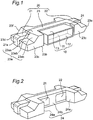
- FIG. 1 is a perspective view showing a configuration of the light emitting device of an embodiment of the present invention.
- FIG. 2 is a perspective view showing a configuration of a base member 20 with a first surface 23a as a mounting surface upward.
- the light emitting device can include the base member 20 having a recess 24, and a light emitting element 10 disposed on a bottom surface 24b of the recess in the base member 20.
- the base member 20 includes a resin-molded body 23, and a first lead 21 and a second lead 22 that are embedded in the resin-molded body 23.
- the resin-molded body 23 includes the first surface 23a which is one of two opposing main surfaces, a second surface 23b which is the other of the two opposing main surfaces, a front surface 23c, a rear surface 23f, a first end surface 23d, and a second end surface 23e, as well as the groove-shaped recess 24 in the front surface 23c.
- the first surface 23a as a mounting surface is shown upside. Accordingly, in a mounted state, the first surface 23a corresponds to a lower surface and the second surface 23b corresponds to an upper surface.
- the recess 24 is formed in the front surface 23c across the front surface 23c so as to penetrate from the first surface 23a to the second surface 23b, and includes the bottom surface 24b of the recess and two side walls 24a.
- the side walls 24a of the recess are preferably inclined such that an opening side of the recess is greater than the recess bottom surface 24b. Mounting of the light emitting element may be facilitated by making the opening side greater.
- the first surface 23a includes a stepped portion on each of a side of the first end surface 23d and a side of the second end surface 23e, and the resin-molded body 23 becomes thin at the stepped portion.
- a part excluding inclined surfaces 23ac and flat surfaces 23ab that are continuous from the corresponding inclined surfaces 23ac that constitute the stepped portions on the side of the first end surface 23d and the side of the second end surface 23e is referred to as a mount surface 23as.
- Examples of a material for molding the resin-molded body 23 can include a thermoplastic resin and a thermosetting resin, and more specifically, resins such as polyphthalamide (PPA), a polycarbonate resin, polyphenylenesulfide (PPS), liquid crystal polymer (LCP), an ABS resin, an epoxy resin, a phenolic resin, an acrylic resin, and a PBT resin. Further, it is possible to improve reflectance of light on the surface of the resin-molded body by mixing a light-reflective material such as titanium oxide into the material for molding. With this, it is possible to cause returning light to be efficiently reflected.
- resins such as polyphthalamide (PPA), a polycarbonate resin, polyphenylenesulfide (PPS), liquid crystal polymer (LCP), an ABS resin, an epoxy resin, a phenolic resin, an acrylic resin, and a PBT resin.
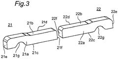
- the first lead 21 includes one end surface 21e and the other end surface 21f.
- the first lead 21 is formed in a pillar shape of a substantial hexahedron elongated in a direction from the one end surface 21e to the other end surface 21f.
- the first lead 21 includes four side surfaces 21a, 21b, 21c, and 21d between the one end surface 21e and the other end surface 21f.
- FIG. 3 shows the first lead 21 and the second lead 22 with their positional relation within the resin-molded body 23 maintained.
- the first lead 21 is embedded in the resin-molded body 23 such that the one end surface 21e is exposed at a central portion of the first end surface 23d of the resin-molded body 23, and a part of the side surface 21b on a side of the one end surface 21e is exposed from the inclined surface 23ac and the flat surface 23ab of the first surface 23a of the resin-molded body 23. A part of the side surface 21a of the first lead 21 on a side of the other end surface 21f is exposed at the bottom surface 24b of the recess of the resin-molded body 23.
- a recess 21g is provided in the side surface 21c of the first lead 21, and the recess prevents the first lead 21 from falling out of the resin-molded body 23.
- the second lead 22 includes one end surface 22e and the other end surface 22f.
- the second lead 22 is formed in a pillar shape of substantial hexahedron elongated in a direction from the one end surface 22e to the other end surface 22f.
- the second lead 22 includes four side surfaces 22a, 22b, 22c, and 22d between the one end surface 22e and the other end surface 22f.
- the second lead 22 is embedded in the resin-molded body 23 such that the one end surface 22e is exposed at a central portion of the second end surface 23e of the resin-molded body 23, and a part of the side surface 22b on a side of the one end surface 22e is exposed from the inclined surface 23ac and the flat surface 23ab of the first surface 23a of the resin-molded body 23.
- a part of the side surface 22a of the second lead 22 on a side of the other end surface 22f is exposed at the bottom surface 24b of the recess of the resin-molded body 23.
- a recess 22g is provided in the side surface 22c of the second lead 22, and the recess prevents the second lead 22 from falling out of the resin-molded body 23.
- the first lead 21 is embedded in the resin-molded body 23 such that the part of the side surface 21b on the side of the one end surface 21e is exposed from the resin-molded body 23, and the second lead 22 is embedded in the resin-molded body 23 such that the part of the side surface 22b on the side of the one end surface 22e is exposed from the resin-molded body 23.
- the present invention is not limited to such an example, and the first lead 21 and the second lead 22 may be embedded in the resin-molded body 23 such that, for example, the side surface 21b on the side of the other end surface 21f and the side surface 22b on the side of the other end surface 22f are exposed while positioned in the same plane as the mount surface 23as.
- first lead 21 and the second lead 22 may be embedded in the resin-molded body 23 such that the side surface 21b on the side of the other end surface 21f and the side surface 22b on the side of the other end surface 22f are exposed while extending from the mount surface 23as.
- each of the first lead 21 and the second lead 22 is formed in a pillar shape of substantial hexahedron elongated in one direction.
- the part of the side surface 21a on the side of the other end surface 21f is exposed at the bottom surface 24b of the recess, and the part on the side of the one end surface 21e of the side surface 21b that is perpendicular to the side surface 21a is constituted as a main external connection surface for connecting to an external circuit.
- the part of the side surface 22a on the side of the other end surface 22f is exposed at the bottom surface 24b of the recess, and the part on the side of the one end surface 22e of the side surface 22b that is perpendicular to the side surface 22a is constituted as a main external connection surface for connecting to an external circuit.
- each of the first lead 21 and the second lead 22 in a pillar shape of substantial hexahedron, it is possible to use one of the two side surfaces that are perpendicular to each other for connection with the light emitting element 10, and the other of the two side surfaces as the external connection surface, and thus to improve heat radiation characteristics.
- the first lead and the second lead may be made of a conductive material including at least one of aluminum, iron, nickel, copper, a copper alloy, stainless steel, and a ferro-alloy including Invar alloy, for example.
- a clad material having a cladding of different types of metals may also be used.
- a thickness of the lead frame is, for example, from 50 ⁇ m to 1000 ⁇ m, and preferably, from 100 ⁇ m to 500 ⁇ m.
- the thickness of the lead frame may be changed depending on the purpose. It is possible to change the thickness of the lead frame by etching (half etching) or press working.
- the base member 20 thus configured may be manufactured in the following manner, for example.
- a mold having a cavity corresponding to the shape of the resin-molded body 23 is prepared. Then, two columnar leads that are to be the first lead 21 and the second lead 22 are positioned in the cavity and fixed at a predetermined distance between their ends. The ends of the columnar leads positioned at the predetermined distance respectively correspond to the other end surface 21f and the other end surface 22f illustrated in FIG. 3 .
- the mold is configured by two or more molds that are separable, and one of the molds includes a projection corresponding to the recess 24, and the other of the molds includes a gate for injecting a resin.
- the resin-molded body After hardening the resin, the resin-molded body is taken out of the mold, and the columnar leads that extend outside the resin-molded body 23 are cut.
- the columnar first lead 21 and the columnar second lead 22 are cut along the first end surface 23d and the second end surface 23e (parallelly) such that the ends on the side of the one end surface 21e and the one end surface 22e project from the resin-molded body 23 by a predetermined length.
- the one end surfaces 21e and 22e respectively constituted by cutting surfaces are provided.
- the one end surface 21e constituted by the cutting surface is preferably perpendicular to the four side surfaces 21a, 21b, 21c, and 21d
- the one end surface 22e constituted by the cutting surface is preferably perpendicular to the four side surfaces 22a, 22b, 22c, and 22d.
- a portion represented by 28 is a gate trace of the resin-molded body 23.
- the base member 20 thus configured is provided with the recess 24 housing the light emitting element so as to penetrate from the first surface 23a to the second surface 23b, and its thickness (a distance between the first surface 23a and the second surface 23b) may be thin as there is no walls on the side of the first surface 23a and on the side of the second surface 23b (hereinafter, referred to as upper and lower walls).
- the recess 24 has no upper and lower walls, light from the light emitting element may leak from the side of the first surface 23a and the side of the second surface 23b, and it is not possible to efficiently extract light emitted from the light emitting element to a front side.
- embodiments of the present invention realize a thin light emitting device capable of efficiently extracting light from the light emitting element to the front side, by using a light emitting element having a reflecting layer provided on the side surfaces.
- Examples of the light emitting element 10 can include a light emitting element chip 11, a light transmissive member 12 disposed on a light-emitting surface of the light emitting element chip 11, and a reflecting layer 13 covering an periphery of the light emitting element chip 11 and an periphery of the light transmissive member 12.
- the light emitting element 10 can be configured such that a side surface of a quadrangular prismatic body defined by a chip mounting surface of the light emitting element chip 11 on which a positive electrode 3a and a negative electrode 3b are provided, an upper surface of the light transmissive member 12, and side surfaces that are perpendicular to the upper surface and the chip mounting surface are covered by the reflecting layer 13, and an outer shape of the light emitting element 10 including the reflecting layer 13 is also in a quadrangular prismatic body.
- the quadrangular prismatic body excluding the reflecting layer 13 is referred to as an inner quadrangular prismatic body
- the quadrangular prismatic body including the reflecting layer 13 is referred to as an outer quadrangular prismatic body.
- the shape of the light emitting element 10 is not limited to quadrangular prismatic body, but manufacturing of the light emitting element 10 is facilitated when the shape of the light emitting element 10 is a quadrangular prismatic body.
- manufacturing of the light emitting element 10 is facilitated when the shape of the light emitting element 10 is a quadrangular prismatic body.
- the light emitting element chip 11 having the positive electrode 3a and the negative electrode 3b on the same surface is prepared.
- the light emitting element chip 11 may be any light emitting element as long as a light-emitting layer made of semiconductor is provided.
- a light emitting element having a light-emitting layer made of nitride semiconductor, especially gallium nitride-based compound semiconductor (particularly InGaN) may be suitably combined with a phosphor, as this type of light emitting element is able to emit intense light in a short wavelength region and a near-ultraviolet region in a visual light range.
- a light emission peak wavelength of outgoing light emitted from light-emitting layer of the light emitting element chip 11 has a light emission spectrum around 240 nm to 500 nm which is in the short wavelength region from the near-ultraviolet light to visible light, preferably 380 nm to 420 nm, and more preferably 450 nm to 470 nm.
- a light emitting element emitting light in this wavelength region is able to emit light of a desired color, in particular white light, in combination with a phosphor of various types.
- the light emitting element 10 may have a light-emitting layer made of such as ZnSe-based, InGaAs-based, or AlInGaP-based semiconductor.
- the light transmissive member 12 provided with a light transmissive substrate 1 and a wavelength conversion layer 2 disposed on one surface of the light transmissive substrate 1 is prepared.
- a wavelength conversion member is disposed on the light transmissive substrate, and cut into the same size as the light emitting element chip 11, for example.
- Examples of the light transmissive substrate 1 include glass substrates made of quartz and borosilicate glass.
- a thickness of the light transmissive substrate 1 is preferably from 30 ⁇ m to 1 mm, and more preferably from 50 ⁇ m to 500 ⁇ m.
- a binder resin mixed with a phosphor described later may be used as the wavelength conversion layer 2.
- the phosphor is selected from phosphors excited by light emitted from the light emitting element chip 11. If, for example, the light emitting element chip 11 is a blue light emitting element and it is desired to configure a white light emitting device, it is preferable to use a phosphor that is excited by blue light and exhibits yellow broad light emission.
- a phosphor include phosphors having a cerium-activated garnet structure (in particular, a phosphor activated by cerium, containing aluminum, and having a garnet structure). As a cerium-activated phosphor exhibits yellow broad light emission, it is possible to realize white light with favorable color rendering properties in combination with blue light emission.
- a phosphor having a garnet structure in particular, a phosphor containing aluminum and having a garnet structure is resistant to heat, light, and moisture, and is able to maintain yellow light emission at high brightness for an extended period of time.
- a YAG-based phosphor (generally abbreviated to YAG) expressed by (Re 1-x Sm x ) 3 (A 1-y Ga y ) 5 O 12 :Ce (0 ⁇ x ⁇ 1, 0 ⁇ y ⁇ 1, where Re is at least one of elements selected from a group consisting of Y, Gd, La, Lu, and Tb).
- a phosphor such as Si 6-Z Al Z O Z N 8-Z :Eu, Lu 3 Al 5 O 12 :Ce, BaMgAl 10 O 17 :Eu, BaMgAl 10 O 17 :Eu, Mn, (Zn, Cd)Zn:Cu, (Sr, Ca) 10 (PO 4 ) 6 C 12 :Eu, Mn, (Sr, Ca) 2 Si 5 N 8 :Eu, CaAlSiB x N 3+x :Eu, K 2 SiF 6 :Mn, or CaAlSiN 3 :Eu is used to adjust color rendering properties of a light source for lighting and color reproducibility in use of backlight.
- a quantum dot phosphor may also be used.
- the wavelength conversion layer 2 may include more than two types of phosphors.
- a first type of the phosphors may be excited by primary light from the light emitting element chip 11 to emit light, and a second type of the phosphors may be excited by secondary light emitted from the first type of the phosphors to emit light.
- two types of phosphors of different chromaticity are used, by adjusting amounts of the two types of phosphors, it is possible to achieve light emission corresponding to an arbitrary chromaticity point within a region defined by connecting chromaticity point of each of the two types of phosphors and the light emitting element on a chromaticity diagram.
- a silicone resin or a modified silicone resin can be used as the binder resin.
- an insulating resin having light transmissivity such as an epoxy resin, a modified epoxy resin, or an acrylic resin may be used.
- a resin having a superior weather resistance such as a hybrid resin including at least one of these resins may also be used.
- Examples of a method of providing the wavelength conversion layer 2 include known methods such as printing, spray coating, compression molding, spin coat, and dispensing.
- the wavelength conversion layer 2 be provided such that a film thickness is uniform and phosphor particles may not be eccentrically located.
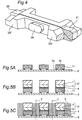
- light emitting element chips 11 are arranged on a sheet 6 in matrix at predetermined intervals with a surface having the positive electrode 3a and the negative electrode 3b downside.
- the predetermined intervals at which the light emitting element chips 11 are arranged are set considering a thickness t of the reflecting layer 13. Specifically, the intervals are set to a value obtained by adding a value that is twice as large as the thickness t of the reflecting layer 13 with a cutting width that will be later described.
- the sheet 6 is provided with an adhesive layer or a sticking layer, for example, on one surface, and the light emitting element chips 11 are maintained at the predetermined intervals by the adhesive layer or the sticking layer.
- the light transmissive member 12 having the wavelength conversion layer 2 is joined onto each of the light emitting element chips 11 by an adhesive member 4.
- the light transmissive substrate 1 is manufactured in a planar shape of a size that is the same as or slightly larger than the light emitting element chip 11, and the wavelength conversion layer 2 is joined to the light emitting element chip 11 via the adhesive member 4 made for example of a silicone resin.
- the adhesive member 4 made for example of a silicone resin.
- a resin 5 constituting the reflecting layer 13 is applied such that the resin 5 is filled between the arranged inner quadrangular columnar bodies.
- a light-reflective material is contained in the resin 5. With this, it is possible to improve light emission efficiency by reflecting light emitted from the side surfaces of the light emitting element chip 11 by the light-reflective material contained in the resin 5 toward the wavelength conversion layer 2. At least one selected from a group constituting of TiO 2 , ZrO 2 , Nb 2 O 5 , Al 2 O 3 , MgF, AlN, SiO 2 , and MgO may be used as the light-reflective material.
- the resin 5 containing the light-reflective material is filled between the arranged light emitting elements chip 11 by applying the resin 5 and spreading the resin 5 using a squeegee.
- the squeegee is moved along the upper surface of the light transmissive substrate 1 of the light transmissive member 12, and causes the resin 5 to fill between the light emitting element chips 11 such that the upper surface of the resin 5 and the upper surface of the light transmissive substrate 1 are positioned in the substantially same plane.
- the hardened resin 5 is cut along a cutting line 7 by dicing, for example, into individual light emitting elements.
- the cutting line 7 is set so as to match a center line between adjacent light emitting element chips 11, for example.
- a distance between the cutting line 7 and the side surface of the light emitting element chip 11 is set such that the thickness t of the reflecting layer 13 after the cutting is a predetermined thickness.
- the light emitting element 10 including the light emitting element chip 11, the light transmissive member 12 disposed on the light-emitting surface of the light emitting element chip 11, the reflecting layer 13 covering the periphery of the light emitting element chip 11 and the light transmissive member 12 is manufactured.
- a leakage of light through the side surface of the inner quadrangular prismatic body is prevented by providing the reflecting layer 13 on or over an entire side surface of the inner quadrangular prismatic body.
- the reflecting layer may be provided on or over a part of the side surface of the inner quadrangular prismatic body to restrict the light-emitting region to a predetermined range.
- the resin 5 constituting the reflecting layer 13 may be provided between the arranged inner quadrangular columnar bodies to a predetermined depth, and then the reflecting layer may be provided on or over a part of the side surface of the inner quadrangular prismatic body.
- the reflecting layer 13 it is possible to appropriately set a region in which the reflecting layer 13 is provided on the side surface of the inner quadrangular prismatic body based on a required light extracting efficiency, the shape of the package recess, and required directional characteristics.
- the light emitting element 10 thus manufactured is mounted on the recess bottom surface 24b of the base member 20 by flip-chip mounting, and thus the light emitting device according to an embodiment of the present invention is completed.
- the example in which the light transmissive member 12 is configured by the light transmissive substrate 1 and the wavelength conversion layer 2 provided on one surface of the light transmissive substrate 1 has been described.
- the present invention is not limited to such an example.
- the light emitting element 10 may be configured by providing the wavelength conversion layer on or over the light emitting element chip 11, and providing the transparent resin layer on or over the wavelength conversion layer.
- the light transmissive member 12 may be configured by a single resin layer containing the phosphor, or by a single resin layer containing no phosphor.
- the light transmissive member 12 may be configured by a plurality of resin layers including or not including the wavelength conversion layer 2.
- the recess 24 housing the light emitting element 10 is provided so as to penetrate from the first surface 23a to the second surface 23b in the base member 20, and there are no upper and lower walls on the sides of the first surface 23a and the second surface 23b. Therefore, the light emitting device according to an embodiment of the present invention may be made thin.
- the reflecting layer 13 is provided on or over the side surface of the light emitting element 10, it is possible to efficiently extract light from the light emitting element to the front side.
- the light emitting device has no upper and lower walls in the recess 24, it is possible to increase a ratio of a volume of the light emitting element 10 in the recess 24, and to make its size smaller and thinner.
- the recess has upper and lower walls, it is necessary to provide a gap above a predetermined level between the upper and lower walls and the light emitting elements in order to facilitate mounting of the light emitting element, the present invention does not require such an extra space for mounting.
- the upper and lower walls is required to be inclined in order to cause light from the light emitting element to be efficiently reflected to a front side in the configuration in which the reflecting layer is provided for the upper and lower walls.
- the reflecting layer 13 is provided integrally with the light emitting element 10 spaced apart from the side walls of the recess, and therefore it is possible to restrict the light-emitting region to a narrower region, and effectively to a predetermined range.
- the expression that the reflecting layer 13 is spaced apart from the side walls of the recess means that there is a distance between the reflecting layer 13 and the side walls of the recess as compared to the case in which the reflecting layer is provided for the side walls of the recess, and a part of the reflecting layer may be in contact with the side walls of the recess, for example.
- the light emitting device is able to restrict the light-emitting region to a desired region by appropriately setting a region in which the reflecting layer 13 is provided.
- the first surface 23a includes the stepped portion on each of the side of the first end surface 23d and the side of the second end surface 23e, and a reservoir for a bonding member (such as soldering) is provided on each of the sides of the first lead 21 and the second lead 22 exposed from the resin-molded body 23.
- a bonding member such as soldering
- the light emitting device improves the heat radiation characteristics using the columnar-shaped first lead 21 and the columnar-shaped second lead 22. Specifically, if the first lead and the second lead are configured using metal flakes as in the conventional technique, the heat radiation characteristics deteriorate as the first lead and the second lead become smaller and thinner.
- the light emitting device improves the heat radiation characteristics by increasing a ratio of metallic components that constitute the first lead 21 and the second lead 22 in the resin-molded body 23 using the columnar-shaped first lead 21 and the columnar-shaped second lead 22. It is preferable that the ratio of the metallic components that constitute the first lead 21 and the second lead 22 in the resin-molded body 23 is as high as possible. This is because both the heat radiation characteristics and facility for implementation are improved as the ratio of the leads increases.
- the first surface 23a includes the stepped portion on each of the side of the first end surface 23d and the side of the second end surface 23e, and an area of the first lead 21 and the second lead 22 exposed from the resin-molded body 23 on the side of the first end surface 23d and on the side of the second end surface 23e is increased. With this, it is possible to more effectively radiate heat in an actual implementation.
- the present disclosure includes the following aspects:
Landscapes
- Engineering & Computer Science (AREA)
- Microelectronics & Electronic Packaging (AREA)
- Computer Hardware Design (AREA)
- Power Engineering (AREA)
- Manufacturing & Machinery (AREA)
- Led Device Packages (AREA)
Description
- The present application claims the benefit of Japanese Patent Application No.
2013-177773, filed on August 29, 2013 - The invention relates to a light emitting device.
- A light emitting device employing a light emitting diode has been widely used as a backlight source for an image display device. One example of a light emitting device as a backlight source for an image display device is provided with a light guide plate and a light emitting device disposed on a side surface of the light guide plate, and configured to emit light emitted from the light emitting device through a light-emitting surface of the light guide plate. Further, as a light emitting device used as a backlight source for an image display device used for a mobile terminal, a side-view type (side surface emission type) light emitting device, as disclosed in
JP2010-3743 A
EP 2 315 263 A1 - As mobile terminals become thinner, even thinner side-view type light emitting devices have become demanded.
- Thus, an object of the present invention is to provide a small and thin side-view type light emitting device capable of efficiently extracting light from a light emitting element to a front side.
- The object can be achieved by the features defined in the claims. Particularly, in order to achieve the above object, a light emitting device for a backlight source, as defined by independent claim 1, includes a base member comprising a resin-molded body having an upper surface, a lower surface, and a front surface having a recess formed in a groove-shaped from the upper surface to the lower surface. A lead is embedded in the resin-molded body. A light emitting element is included, having a light emitting element chip and a reflecting layer limiting a light-emitting region to a predetermined range. The reflecting layer is disposed on a side surface of the light emitting element chip. The light emitting element is disposed on a bottom surface of the recess. The reflecting layer is provided integrally with the light emitting element and positioned spaced apart from the side walls of the recess.
- According to the light emitting device thus configured, it is possible to provide a small and thin side-view type light emitting device capable of efficiently extracting light from the light emitting element to a front side.
The invention is described in detail in conjunction with the drawings, in which: -
FIG. 1 is a perspective view showing a configuration of a light emitting device of an embodiment according to the present invention, -
FIG. 2 is a perspective view showing a front surface side of abase member 20 of the embodiment, -
FIG. 3 is a perspective view showing a configuration of a first lead and a second lead embedded in the base member of the embodiment, -
FIG. 4 is a perspective view showing a rear surface side of thebase member 20 of the embodiment, and -
FIGS. 5A - 5C are sectional views showing a process of manufacturing a light emitting element used in the light emitting device of the embodiment. - Hereinafter, a light emitting device of embodiments of the present invention will be described with reference to the drawings.
-
FIG. 1 is a perspective view showing a configuration of the light emitting device of an embodiment of the present invention.FIG. 2 is a perspective view showing a configuration of abase member 20 with afirst surface 23a as a mounting surface upward. - Referring to
FIG. 1 , the light emitting device can include thebase member 20 having arecess 24, and alight emitting element 10 disposed on abottom surface 24b of the recess in thebase member 20. - The
base member 20 includes a resin-moldedbody 23, and afirst lead 21 and asecond lead 22 that are embedded in the resin-moldedbody 23. - The resin-molded
body 23 includes thefirst surface 23a which is one of two opposing main surfaces, asecond surface 23b which is the other of the two opposing main surfaces, afront surface 23c, arear surface 23f, afirst end surface 23d, and asecond end surface 23e, as well as the groove-shaped recess 24 in thefront surface 23c. As described above, inFIG. 1 and other drawings, thefirst surface 23a as a mounting surface is shown upside. Accordingly, in a mounted state, thefirst surface 23a corresponds to a lower surface and thesecond surface 23b corresponds to an upper surface. Therecess 24 is formed in thefront surface 23c across thefront surface 23c so as to penetrate from thefirst surface 23a to thesecond surface 23b, and includes thebottom surface 24b of the recess and twoside walls 24a. Theside walls 24a of the recess are preferably inclined such that an opening side of the recess is greater than therecess bottom surface 24b. Mounting of the light emitting element may be facilitated by making the opening side greater. - According to the resin-molded
body 23, thefirst surface 23a includes a stepped portion on each of a side of thefirst end surface 23d and a side of thesecond end surface 23e, and the resin-moldedbody 23 becomes thin at the stepped portion. In thefirst surface 23a, a part excluding inclined surfaces 23ac and flat surfaces 23ab that are continuous from the corresponding inclined surfaces 23ac that constitute the stepped portions on the side of thefirst end surface 23d and the side of thesecond end surface 23e is referred to as a mount surface 23as. - Examples of a material for molding the resin-molded
body 23 can include a thermoplastic resin and a thermosetting resin, and more specifically, resins such as polyphthalamide (PPA), a polycarbonate resin, polyphenylenesulfide (PPS), liquid crystal polymer (LCP), an ABS resin, an epoxy resin, a phenolic resin, an acrylic resin, and a PBT resin. Further, it is possible to improve reflectance of light on the surface of the resin-molded body by mixing a light-reflective material such as titanium oxide into the material for molding. With this, it is possible to cause returning light to be efficiently reflected. - As illustrated in
FIG. 3 , thefirst lead 21 includes oneend surface 21e and theother end surface 21f. Thefirst lead 21 is formed in a pillar shape of a substantial hexahedron elongated in a direction from the oneend surface 21e to theother end surface 21f. Thefirst lead 21 includes fourside surfaces end surface 21e and theother end surface 21f.FIG. 3 shows thefirst lead 21 and thesecond lead 22 with their positional relation within the resin-moldedbody 23 maintained. - The
first lead 21 is embedded in the resin-moldedbody 23 such that the oneend surface 21e is exposed at a central portion of thefirst end surface 23d of the resin-moldedbody 23, and a part of theside surface 21b on a side of the oneend surface 21e is exposed from the inclined surface 23ac and the flat surface 23ab of thefirst surface 23a of the resin-moldedbody 23. A part of theside surface 21a of thefirst lead 21 on a side of theother end surface 21f is exposed at thebottom surface 24b of the recess of the resin-moldedbody 23. Arecess 21g is provided in theside surface 21c of thefirst lead 21, and the recess prevents thefirst lead 21 from falling out of the resin-moldedbody 23. - As illustrated in
FIG. 3 , thesecond lead 22 includes oneend surface 22e and theother end surface 22f. Thesecond lead 22 is formed in a pillar shape of substantial hexahedron elongated in a direction from the oneend surface 22e to theother end surface 22f. Thesecond lead 22 includes fourside surfaces end surface 22e and theother end surface 22f. - As illustrated in
FIG. 1 , thesecond lead 22 is embedded in the resin-moldedbody 23 such that the oneend surface 22e is exposed at a central portion of thesecond end surface 23e of the resin-moldedbody 23, and a part of theside surface 22b on a side of the oneend surface 22e is exposed from the inclined surface 23ac and the flat surface 23ab of thefirst surface 23a of the resin-moldedbody 23. A part of theside surface 22a of thesecond lead 22 on a side of theother end surface 22f is exposed at thebottom surface 24b of the recess of the resin-moldedbody 23. Arecess 22g is provided in theside surface 22c of thesecond lead 22, and the recess prevents thesecond lead 22 from falling out of the resin-moldedbody 23. - According to the light emitting device of this embodiment, the
first lead 21 is embedded in the resin-moldedbody 23 such that the part of theside surface 21b on the side of the oneend surface 21e is exposed from the resin-moldedbody 23, and thesecond lead 22 is embedded in the resin-moldedbody 23 such that the part of theside surface 22b on the side of the oneend surface 22e is exposed from the resin-moldedbody 23. However, the present invention is not limited to such an example, and thefirst lead 21 and thesecond lead 22 may be embedded in the resin-moldedbody 23 such that, for example, theside surface 21b on the side of theother end surface 21f and theside surface 22b on the side of theother end surface 22f are exposed while positioned in the same plane as the mount surface 23as. Alternatively, thefirst lead 21 and thesecond lead 22 may be embedded in the resin-moldedbody 23 such that theside surface 21b on the side of theother end surface 21f and theside surface 22b on the side of theother end surface 22f are exposed while extending from the mount surface 23as. - As illustrated in
FIG. 3 , in some embodiments of the present invention, each of thefirst lead 21 and thesecond lead 22 is formed in a pillar shape of substantial hexahedron elongated in one direction. The part of theside surface 21a on the side of theother end surface 21f is exposed at thebottom surface 24b of the recess, and the part on the side of the oneend surface 21e of theside surface 21b that is perpendicular to theside surface 21a is constituted as a main external connection surface for connecting to an external circuit. The part of theside surface 22a on the side of theother end surface 22f is exposed at thebottom surface 24b of the recess, and the part on the side of the oneend surface 22e of theside surface 22b that is perpendicular to theside surface 22a is constituted as a main external connection surface for connecting to an external circuit. - In this manner, according to some embodiments of the present invention, by forming each of the
first lead 21 and thesecond lead 22 in a pillar shape of substantial hexahedron, it is possible to use one of the two side surfaces that are perpendicular to each other for connection with thelight emitting element 10, and the other of the two side surfaces as the external connection surface, and thus to improve heat radiation characteristics. - The first lead and the second lead may be made of a conductive material including at least one of aluminum, iron, nickel, copper, a copper alloy, stainless steel, and a ferro-alloy including Invar alloy, for example. A clad material having a cladding of different types of metals may also be used. Further, it is preferable that a surface of a lead frame be plated by gold, silver, nickel, palladium, or an alloy of these metals
- Moreover, a thickness of the lead frame is, for example, from 50 µm to 1000 µm, and preferably, from 100 µm to 500 µm. In addition, the thickness of the lead frame may be changed depending on the purpose. It is possible to change the thickness of the lead frame by etching (half etching) or press working.
- The
base member 20 thus configured may be manufactured in the following manner, for example. - First, a mold having a cavity corresponding to the shape of the resin-molded
body 23 is prepared. Then, two columnar leads that are to be thefirst lead 21 and thesecond lead 22 are positioned in the cavity and fixed at a predetermined distance between their ends. The ends of the columnar leads positioned at the predetermined distance respectively correspond to theother end surface 21f and theother end surface 22f illustrated inFIG. 3 . - For example, the mold is configured by two or more molds that are separable, and one of the molds includes a projection corresponding to the
recess 24, and the other of the molds includes a gate for injecting a resin. - Next, a resin is injected into the cavity in which the
first lead 21 and thesecond lead 22 are fixed, and the resin is hardened. - After hardening the resin, the resin-molded body is taken out of the mold, and the columnar leads that extend outside the resin-molded
body 23 are cut. - The columnar
first lead 21 and the columnarsecond lead 22 are cut along thefirst end surface 23d and thesecond end surface 23e (parallelly) such that the ends on the side of the oneend surface 21e and the oneend surface 22e project from the resin-moldedbody 23 by a predetermined length. In this manner, the one end surfaces 21e and 22e respectively constituted by cutting surfaces are provided. The oneend surface 21e constituted by the cutting surface is preferably perpendicular to the fourside surfaces end surface 22e constituted by the cutting surface is preferably perpendicular to the fourside surfaces - In
FIG. 4 , a portion represented by 28 is a gate trace of the resin-moldedbody 23. - The
base member 20 thus configured is provided with therecess 24 housing the light emitting element so as to penetrate from thefirst surface 23a to thesecond surface 23b, and its thickness (a distance between thefirst surface 23a and thesecond surface 23b) may be thin as there is no walls on the side of thefirst surface 23a and on the side of thesecond surface 23b (hereinafter, referred to as upper and lower walls). - However, as the
recess 24 has no upper and lower walls, light from the light emitting element may leak from the side of thefirst surface 23a and the side of thesecond surface 23b, and it is not possible to efficiently extract light emitted from the light emitting element to a front side. - Therefore, embodiments of the present invention realize a thin light emitting device capable of efficiently extracting light from the light emitting element to the front side, by using a light emitting element having a reflecting layer provided on the side surfaces.
- Examples of the
light emitting element 10 can include a light emittingelement chip 11, alight transmissive member 12 disposed on a light-emitting surface of the light emittingelement chip 11, and a reflectinglayer 13 covering an periphery of the light emittingelement chip 11 and an periphery of thelight transmissive member 12. Thelight emitting element 10 can be configured such that a side surface of a quadrangular prismatic body defined by a chip mounting surface of the light emittingelement chip 11 on which apositive electrode 3a and anegative electrode 3b are provided, an upper surface of thelight transmissive member 12, and side surfaces that are perpendicular to the upper surface and the chip mounting surface are covered by the reflectinglayer 13, and an outer shape of thelight emitting element 10 including the reflectinglayer 13 is also in a quadrangular prismatic body. Hereinafter, the quadrangular prismatic body excluding the reflectinglayer 13 is referred to as an inner quadrangular prismatic body, and the quadrangular prismatic body including the reflectinglayer 13 is referred to as an outer quadrangular prismatic body. According to embodiments of the present invention, the shape of thelight emitting element 10 is not limited to quadrangular prismatic body, but manufacturing of thelight emitting element 10 is facilitated when the shape of thelight emitting element 10 is a quadrangular prismatic body. In the following, one example of a method of manufacturing thelight emitting element 10 will be described. - The light emitting
element chip 11 having thepositive electrode 3a and thenegative electrode 3b on the same surface is prepared. - The light emitting
element chip 11 may be any light emitting element as long as a light-emitting layer made of semiconductor is provided. In particular, a light emitting element having a light-emitting layer made of nitride semiconductor, especially gallium nitride-based compound semiconductor (particularly InGaN) may be suitably combined with a phosphor, as this type of light emitting element is able to emit intense light in a short wavelength region and a near-ultraviolet region in a visual light range. Desirably, a light emission peak wavelength of outgoing light emitted from light-emitting layer of the light emittingelement chip 11 has a light emission spectrum around 240 nm to 500 nm which is in the short wavelength region from the near-ultraviolet light to visible light, preferably 380 nm to 420 nm, and more preferably 450 nm to 470 nm. A light emitting element emitting light in this wavelength region is able to emit light of a desired color, in particular white light, in combination with a phosphor of various types. Alternatively, thelight emitting element 10 may have a light-emitting layer made of such as ZnSe-based, InGaAs-based, or AlInGaP-based semiconductor. - The
light transmissive member 12 provided with a light transmissive substrate 1 and awavelength conversion layer 2 disposed on one surface of the light transmissive substrate 1 is prepared. - Specifically, a wavelength conversion member is disposed on the light transmissive substrate, and cut into the same size as the light emitting
element chip 11, for example. - Examples of the light transmissive substrate 1 include glass substrates made of quartz and borosilicate glass. A thickness of the light transmissive substrate 1 is preferably from 30 µm to 1 mm, and more preferably from 50 µm to 500 µm.
- As the
wavelength conversion layer 2, a binder resin mixed with a phosphor described later may be used. - The phosphor is selected from phosphors excited by light emitted from the light emitting
element chip 11. If, for example, the light emittingelement chip 11 is a blue light emitting element and it is desired to configure a white light emitting device, it is preferable to use a phosphor that is excited by blue light and exhibits yellow broad light emission. Examples of such a phosphor include phosphors having a cerium-activated garnet structure (in particular, a phosphor activated by cerium, containing aluminum, and having a garnet structure). As a cerium-activated phosphor exhibits yellow broad light emission, it is possible to realize white light with favorable color rendering properties in combination with blue light emission. A phosphor having a garnet structure, in particular, a phosphor containing aluminum and having a garnet structure is resistant to heat, light, and moisture, and is able to maintain yellow light emission at high brightness for an extended period of time. For example, it is preferable to use, as the phosphor, a YAG-based phosphor (generally abbreviated to YAG) expressed by (Re1-xSmx)3(A1-yGay)5O12:Ce (0 ≤ x < 1, 0 ≤ y ≤ 1, where Re is at least one of elements selected from a group consisting of Y, Gd, La, Lu, and Tb). Further, other than the yellow phosphor, a phosphor such as Si6-ZAlZOZN8-Z:Eu, Lu3Al5O12:Ce, BaMgAl10O17:Eu, BaMgAl10O17:Eu, Mn, (Zn, Cd)Zn:Cu, (Sr, Ca)10(PO4)6C12:Eu, Mn, (Sr, Ca)2Si5N8:Eu, CaAlSiBxN3+x:Eu, K2SiF6:Mn, or CaAlSiN3:Eu is used to adjust color rendering properties of a light source for lighting and color reproducibility in use of backlight. Alternatively, a quantum dot phosphor may also be used. - When a light emission wavelength of the light emitting
element chip 11 is a short wavelength, thewavelength conversion layer 2 may include more than two types of phosphors. A first type of the phosphors may be excited by primary light from the light emittingelement chip 11 to emit light, and a second type of the phosphors may be excited by secondary light emitted from the first type of the phosphors to emit light. In addition, when two types of phosphors of different chromaticity are used, by adjusting amounts of the two types of phosphors, it is possible to achieve light emission corresponding to an arbitrary chromaticity point within a region defined by connecting chromaticity point of each of the two types of phosphors and the light emitting element on a chromaticity diagram. - As the binder resin, a silicone resin or a modified silicone resin can be used. In addition, an insulating resin having light transmissivity such as an epoxy resin, a modified epoxy resin, or an acrylic resin may be used. Further, a resin having a superior weather resistance such as a hybrid resin including at least one of these resins may also be used.
- Examples of a method of providing the
wavelength conversion layer 2 include known methods such as printing, spray coating, compression molding, spin coat, and dispensing. - It is preferable that the
wavelength conversion layer 2 be provided such that a film thickness is uniform and phosphor particles may not be eccentrically located. Among the above listed methods of providing a phosphor layer, it is preferable to use printing, spray coating, or compression molding. - As illustrated in
FIG. 5(a) , light emitting element chips 11 are arranged on asheet 6 in matrix at predetermined intervals with a surface having thepositive electrode 3a and thenegative electrode 3b downside. Here, the predetermined intervals at which the light emitting element chips 11 are arranged are set considering a thickness t of the reflectinglayer 13. Specifically, the intervals are set to a value obtained by adding a value that is twice as large as the thickness t of the reflectinglayer 13 with a cutting width that will be later described. Further, thesheet 6 is provided with an adhesive layer or a sticking layer, for example, on one surface, and the light emitting element chips 11 are maintained at the predetermined intervals by the adhesive layer or the sticking layer. - As illustrated in
FIG. 5(b) , thelight transmissive member 12 having thewavelength conversion layer 2 is joined onto each of the light emitting element chips 11 by anadhesive member 4. - For example, the light transmissive substrate 1 is manufactured in a planar shape of a size that is the same as or slightly larger than the light emitting
element chip 11, and thewavelength conversion layer 2 is joined to the light emittingelement chip 11 via theadhesive member 4 made for example of a silicone resin. Through the above steps, a plurality of inner quadrangular columnar bodies each having the light emittingelement chip 11 and thelight transmissive member 12 are arranged on thesheet 6. - As illustrated in
FIG. 5(c) , aresin 5 constituting the reflectinglayer 13 is applied such that theresin 5 is filled between the arranged inner quadrangular columnar bodies. - A light-reflective material is contained in the
resin 5. With this, it is possible to improve light emission efficiency by reflecting light emitted from the side surfaces of the light emittingelement chip 11 by the light-reflective material contained in theresin 5 toward thewavelength conversion layer 2. At least one selected from a group constituting of TiO2, ZrO2, Nb2O5, Al2O3, MgF, AlN, SiO2, and MgO may be used as the light-reflective material. - For example, the
resin 5 containing the light-reflective material is filled between the arranged light emittingelements chip 11 by applying theresin 5 and spreading theresin 5 using a squeegee. At this time, the squeegee is moved along the upper surface of the light transmissive substrate 1 of thelight transmissive member 12, and causes theresin 5 to fill between the light emitting element chips 11 such that the upper surface of theresin 5 and the upper surface of the light transmissive substrate 1 are positioned in the substantially same plane. - As illustrated in
FIG. 5(c) , after hardening theresin 5, thehardened resin 5 is cut along acutting line 7 by dicing, for example, into individual light emitting elements. Thecutting line 7 is set so as to match a center line between adjacent light emitting element chips 11, for example. A distance between the cuttingline 7 and the side surface of the light emittingelement chip 11 is set such that the thickness t of the reflectinglayer 13 after the cutting is a predetermined thickness. - In this manner, the
light emitting element 10 including the light emittingelement chip 11, thelight transmissive member 12 disposed on the light-emitting surface of the light emittingelement chip 11, the reflectinglayer 13 covering the periphery of the light emittingelement chip 11 and thelight transmissive member 12 is manufactured. According to thelight emitting element 10 of this embodiment, a leakage of light through the side surface of the inner quadrangular prismatic body is prevented by providing the reflectinglayer 13 on or over an entire side surface of the inner quadrangular prismatic body. However, the present invention is not limited to such an example. The reflecting layer may be provided on or over a part of the side surface of the inner quadrangular prismatic body to restrict the light-emitting region to a predetermined range. For example, in the step of filling the resin, theresin 5 constituting the reflectinglayer 13 may be provided between the arranged inner quadrangular columnar bodies to a predetermined depth, and then the reflecting layer may be provided on or over a part of the side surface of the inner quadrangular prismatic body. Specifically, according to embodiments of the present invention, it is possible to appropriately set a region in which the reflectinglayer 13 is provided on the side surface of the inner quadrangular prismatic body based on a required light extracting efficiency, the shape of the package recess, and required directional characteristics. - The
light emitting element 10 thus manufactured is mounted on therecess bottom surface 24b of thebase member 20 by flip-chip mounting, and thus the light emitting device according to an embodiment of the present invention is completed. - According to certain embodiments, the example in which the
light transmissive member 12 is configured by the light transmissive substrate 1 and thewavelength conversion layer 2 provided on one surface of the light transmissive substrate 1 has been described. However, the present invention is not limited to such an example. For example, thelight emitting element 10 may be configured by providing the wavelength conversion layer on or over the light emittingelement chip 11, and providing the transparent resin layer on or over the wavelength conversion layer. Further, thelight transmissive member 12 may be configured by a single resin layer containing the phosphor, or by a single resin layer containing no phosphor. Moreover, thelight transmissive member 12 may be configured by a plurality of resin layers including or not including thewavelength conversion layer 2. - In the light emitting device according to embodiments of the present invention, the
recess 24 housing thelight emitting element 10 is provided so as to penetrate from thefirst surface 23a to thesecond surface 23b in thebase member 20, and there are no upper and lower walls on the sides of thefirst surface 23a and thesecond surface 23b. Therefore, the light emitting device according to an embodiment of the present invention may be made thin. - Further, as the reflecting
layer 13 is provided on or over the side surface of thelight emitting element 10, it is possible to efficiently extract light from the light emitting element to the front side. - As the light emitting device according to an embodiment of the present invention thus configured has no upper and lower walls in the
recess 24, it is possible to increase a ratio of a volume of thelight emitting element 10 in therecess 24, and to make its size smaller and thinner. Specifically, if the recess has upper and lower walls, it is necessary to provide a gap above a predetermined level between the upper and lower walls and the light emitting elements in order to facilitate mounting of the light emitting element, the present invention does not require such an extra space for mounting. Furthermore, the upper and lower walls is required to be inclined in order to cause light from the light emitting element to be efficiently reflected to a front side in the configuration in which the reflecting layer is provided for the upper and lower walls. Therefore, it is necessary to provide a gap between the upper and lower walls and the light emitting element in order to allow the upper and lower walls to be inclined. However, with the present invention, it is not necessary to provide a gap for such a purpose. Therefore, it is not necessary to provide an extra gap in addition to the thickness of the upper and lower walls that prevents the light emitting device from being made thinner, and the light emitting device may be substantially made as thin as the thickness of thelight emitting element 10. - As described above, according to embodiments of the present invention, it is possible to provide an extremely small and thin side-view type light emitting device capable of efficiently extracting light from the light emitting element to the front side.
- According to an embodiment of the light emitting device of the present invention, the reflecting
layer 13 is provided integrally with thelight emitting element 10 spaced apart from the side walls of the recess, and therefore it is possible to restrict the light-emitting region to a narrower region, and effectively to a predetermined range. Here, the expression that the reflectinglayer 13 is spaced apart from the side walls of the recess means that there is a distance between the reflectinglayer 13 and the side walls of the recess as compared to the case in which the reflecting layer is provided for the side walls of the recess, and a part of the reflecting layer may be in contact with the side walls of the recess, for example. - Specifically, while it is difficult to restrict the light-emitting region to a region narrower than an opening of the recess with the conventional light emitting device configured such that the reflecting layer is provided for the upper and lower walls and the side walls of the recess, the light emitting device according to an embodiment of the present invention is able to restrict the light-emitting region to a desired region by appropriately setting a region in which the reflecting
layer 13 is provided. - In the resin-molded
body 23, thefirst surface 23a includes the stepped portion on each of the side of thefirst end surface 23d and the side of thesecond end surface 23e, and a reservoir for a bonding member (such as soldering) is provided on each of the sides of thefirst lead 21 and thesecond lead 22 exposed from the resin-moldedbody 23. With this, it is possible to prevent the light emitting device from floating when mounted, and to suppress an increase of the height when mounting. - Furthermore, the light emitting device according to embodiments of the present invention improves the heat radiation characteristics using the columnar-shaped
first lead 21 and the columnar-shapedsecond lead 22. Specifically, if the first lead and the second lead are configured using metal flakes as in the conventional technique, the heat radiation characteristics deteriorate as the first lead and the second lead become smaller and thinner. However, the light emitting device according to embodiments of the present invention improves the heat radiation characteristics by increasing a ratio of metallic components that constitute thefirst lead 21 and thesecond lead 22 in the resin-moldedbody 23 using the columnar-shapedfirst lead 21 and the columnar-shapedsecond lead 22. It is preferable that the ratio of the metallic components that constitute thefirst lead 21 and thesecond lead 22 in the resin-moldedbody 23 is as high as possible. This is because both the heat radiation characteristics and facility for implementation are improved as the ratio of the leads increases. - Further, in the resin-molded
body 23, thefirst surface 23a includes the stepped portion on each of the side of thefirst end surface 23d and the side of thesecond end surface 23e, and an area of thefirst lead 21 and thesecond lead 22 exposed from the resin-moldedbody 23 on the side of thefirst end surface 23d and on the side of thesecond end surface 23e is increased. With this, it is possible to more effectively radiate heat in an actual implementation. - The present disclosure includes the following aspects:
- The first aspect:
- a light emitting device comprising:
- a base member comprising:
- a resin-molded body having an upper surface, a lower surface and a front surface having a recess formed in a groove-shaped from the upper surface to the lower surface; and
- a lead embedded in the resin-molded body;
- said light emitting device further comprising a light emitting element comprising:
- a light emitting element chip; and
- a reflecting layer limiting a light-emitting region to a predetermined range, the reflecting layer being disposed on or over a side surface of the light emitting element,
- wherein the light emitting element is disposed on a bottom surface of the recess.
- a base member comprising:
- a light emitting device comprising:
- The second aspect:
- the light emitting device according to the first aspect, wherein
- the light emitting element further comprises a light transmissive member transmitting light emitted from the light emitting element chip.
- The third aspect:
- the light emitting device according to the second aspect, wherein
- the reflecting layer covers a periphery of the light emitting element chip and the light transmissive member.
- The fourth aspect:
- the light emitting device according to any one of the first to third aspects, wherein
- the reflecting layer is positioned spaced apart from a side wall of the recess.
- The fifth aspect:
- the light emitting device according to the fourth aspect, wherein
- the side wall of the recess is inclined such that an opening side of the recess is greater than the bottom surface.
- The sixth aspect:
- the light emitting device according to any one of the first to fifth aspects, wherein
- the light emitting element is formed in a shape of a quadrangular prismatic body.
- The seventh aspect:
- the light emitting device according to the second or third aspect, wherein
- the light transmissive member includes:
- a wavelength conversion layer disposed on or over a light-emitting surface of the light emitting element chip; and
- a light transmissive substrate disposed on or over the wavelength conversion layer, and wherein
- the reflecting layer covers a side surface of light emitting element chip and a side surface of the wavelength conversion layer.
- The eighth aspect:
- the light emitting device according to the seventh aspect, wherein
- the reflecting layer further covers a side surface of the light transmissive substrate.
- The ninth aspect:
- the light emitting device according to any one of the first to eighth aspects, wherein
- the lead is formed in a pillar shape having four side surfaces between two end surfaces, a part of one of the four side surfaces is exposed at the bottom surface of the recess, and a part of an another side surface which is perpendicular to the one side surface is configured as an external connection surface.
- The tenth aspect:
- the light emitting device according to the ninth aspect, wherein
- a cutting surface of the lead is perpendicular to the four side surfaces.
- The eleventh aspect:
- the light emitting device according to any one of the first to tenth aspects, wherein
- the lower surface of the resin-molded body has a stepped portion.
- The twelfth aspect:
- the light emitting device according to the seventh or eighth aspect, wherein the wavelength conversion layer comprises a quantum dot phosphor.
- The thirteenth aspect:
- the light emitting device according to any one of the first to twelfth aspects, wherein a side surface of the lead has a recess.
- The fourteenth aspect:
- a light emitting device comprising:
- a base member comprising:
- a resin-molded body having a recess formed in a groove-shaped from one surface to another surface opposed to said one surface; and
- a lead embedded in the resin-molded body;
- said light emitting device further comprising a light emitting element comprising:
- a light emitting element chip; and
- a reflecting layer being disposed on or over a side surface of the light emitting element,
- wherein the light emitting element is disposed on a bottom surface of the recess.
- a base member comprising:
- a light emitting device comprising:
- The fifteenth aspect:
- the light emitting device according to the fourteenth aspect, wherein
- the light emitting element further comprises a light transmissive member transmitting light emitted from the light emitting element chip.
- The sixteenth aspect:
- the light emitting device according to the fifteenth aspect, wherein
- the reflecting layer covers a periphery of the light emitting element chip and the light transmissive member.
- The seventeenth aspect:
- the light emitting device according to the fiftheenth or sixteenth aspect, wherein
- the light transmissive member comprises:
- a wavelength conversion layer disposed on or over a light-emitting surface of the light emitting element chip; and
- a light transmissive substrate disposed on or over the wavelength conversion layer, and wherein
- the reflecting layer covers a side surface of light emitting element chip and a side surface of the wavelength conversion layer.
- The eighteenth aspect:
- the light emitting device according to any one of the fourteenth to seventeenth aspects, wherein
- the lead is formed in a pillar shape having four side surfaces between two end surfaces, a part of one of the four side surfaces is exposed at the bottom surface of the recess, and a part of an another side surface which is perpendicular to the one side surface is configured as an external connection surface.
- The nineteenth aspect:
- the light emitting device according to any one of the fourteenth to eighteenth aspects, wherein the lower surface of the resin-molded body has a stepped portion.
Claims (12)
- A light emitting device for a backlight source of an image display, the light emitting element comprising:a base member comprising:a resin-molded body having an upper surface, a lower surface and a front surface having a recess formed in a groove-shaped from the upper surface to the lower surface; anda lead embedded in the resin-molded body;said light emitting device further comprising a light emitting element comprising:a light emitting element chip; anda reflecting layer limiting a light-emitting region to a predetermined range,wherein the light emitting element is disposed on a bottom surface of the recess, characterized in that the reflecting layer is disposed on a side surface of the light emitting element chip,the reflecting layer is provided integrally with the light emitting element and the reflecting layer is positioned spaced apart from the side walls of the recess.
- The light emitting device according to claim 1, wherein the light emitting element further comprises a light transmissive member transmitting light emitted from the light emitting element chip.
- The light emitting device according to claim 2, wherein the reflecting layer covers a periphery of the light emitting element chip and the light transmissive member.
- The light emitting device according to any one of claims 1 to 3, wherein the side wall of the recess is inclined such that an opening side of the recess is greater than the bottom surface.
- The light emitting device according to any one of claims 1 to 4, wherein the light emitting element is formed in a shape of a quadrangular prismatic body.
- The light emitting device according to claim 2 or 3, wherein the light transmissive member includes:a wavelength conversion layer disposed on or over a light-emitting surface of the light emitting element chip; anda light transmissive substrate disposed on or over the wavelength conversion layer, and whereinthe reflecting layer covers a side surface of light emitting element chip and a side surface of the wavelength conversion layer.
- The light emitting device according to claim 6, wherein the reflecting layer further covers a side surface of the light transmissive substrate.
- The light emitting device according to any one of claims 1 to 7, wherein the lead is formed in a pillar shape having four side surfaces between two end surfaces, a part of one of the four side surfaces is exposed at the bottom surface of the recess, and a part of an another side surface which is perpendicular to the one side surface is configured as an external connection surface.
- The light emitting device according to claim 8, wherein a cutting surface of the lead is perpendicular to the four side surfaces.
- The light emitting device according to any one of claims 1 to 9, wherein the lower surface of the resin-molded body has a stepped portion.
- The light emitting device according to claim 6 or 7, wherein the wavelength conversion layer comprises a quantum dot phosphor.
- The light emitting device according to any one of claims 1 to 11, wherein a side surface of the lead has a recess.
Applications Claiming Priority (1)
| Application Number | Priority Date | Filing Date | Title |
|---|---|---|---|
| JP2013177773A JP6236999B2 (en) | 2013-08-29 | 2013-08-29 | Light emitting device |
Publications (2)
| Publication Number | Publication Date |
|---|---|
| EP2843718A1 EP2843718A1 (en) | 2015-03-04 |
| EP2843718B1 true EP2843718B1 (en) | 2017-11-29 |
Family
ID=51417185
Family Applications (1)
| Application Number | Title | Priority Date | Filing Date |
|---|---|---|---|
| EP14182481.3A Active EP2843718B1 (en) | 2013-08-29 | 2014-08-27 | Light emitting device |
Country Status (6)
| Country | Link |
|---|---|
| US (2) | US10109779B2 (en) |
| EP (1) | EP2843718B1 (en) |
| JP (1) | JP6236999B2 (en) |
| KR (1) | KR102161069B1 (en) |
| CN (1) | CN104425701B (en) |
| TW (1) | TWI680592B (en) |
Families Citing this family (5)
| Publication number | Priority date | Publication date | Assignee | Title |
|---|---|---|---|---|
| EP3098861B1 (en) * | 2015-05-29 | 2020-05-06 | Nichia Corporation | Light emitting device, and method of manufacturing a light emitting device |
| KR102674066B1 (en) * | 2016-11-11 | 2024-06-13 | 삼성전자주식회사 | Light emitting device package |
| DE102017116279B4 (en) * | 2017-07-19 | 2023-08-03 | OSRAM Opto Semiconductors Gesellschaft mit beschränkter Haftung | Process for producing a large number of conversion elements and optoelectronic component |
| CN112490224A (en) * | 2020-11-27 | 2021-03-12 | 广东晶科电子股份有限公司 | Light-emitting device and manufacturing method thereof |
| TWI821731B (en) * | 2021-08-23 | 2023-11-11 | 啟端光電股份有限公司 | Bottom-emission light-emitting diode display |
Citations (1)
| Publication number | Priority date | Publication date | Assignee | Title |
|---|---|---|---|---|
| EP2315263A1 (en) * | 2008-07-29 | 2011-04-27 | Nichia Corporation | Light-emitting device |
Family Cites Families (31)
| Publication number | Priority date | Publication date | Assignee | Title |
|---|---|---|---|---|
| TWI292961B (en) * | 2002-09-05 | 2008-01-21 | Nichia Corp | Semiconductor device and an optical device using the semiconductor device |
| DE102004021233A1 (en) | 2004-04-30 | 2005-12-01 | Osram Opto Semiconductors Gmbh | LED array |
| JP2006269448A (en) * | 2005-03-22 | 2006-10-05 | Stanley Electric Co Ltd | Led |
| EP1875780A2 (en) * | 2005-04-19 | 2008-01-09 | Philips Intellectual Property & Standards GmbH | Illumination system comprising a red-emitting ceramic luminescence converter |
| TWI302041B (en) * | 2006-01-19 | 2008-10-11 | Everlight Electronics Co Ltd | Light emitting diode packaging structure |
| JP4857791B2 (en) * | 2006-02-01 | 2012-01-18 | 日亜化学工業株式会社 | Manufacturing method of semiconductor device |
| WO2007108616A1 (en) * | 2006-03-17 | 2007-09-27 | Seoul Semiconductor Co., Ltd. | Side-view light emitting diode package having a reflector |
| JP4952215B2 (en) * | 2006-08-17 | 2012-06-13 | 日亜化学工業株式会社 | Light emitting device |
| JP5205773B2 (en) | 2006-11-07 | 2013-06-05 | 日亜化学工業株式会社 | Light emitting device |
| JP2008187030A (en) | 2007-01-30 | 2008-08-14 | Stanley Electric Co Ltd | Light emitting device |
| JP5132961B2 (en) * | 2007-03-19 | 2013-01-30 | ハリソン東芝ライティング株式会社 | Optical semiconductor device and manufacturing method thereof |
| KR101374895B1 (en) * | 2007-03-31 | 2014-03-17 | 서울반도체 주식회사 | Side view type light emitting diode package and method for fabricating the same diode |
| JP2009032746A (en) * | 2007-07-24 | 2009-02-12 | Harison Toshiba Lighting Corp | Light-emitting device and light-emitting unit |
| JP2009038184A (en) * | 2007-08-01 | 2009-02-19 | Harison Toshiba Lighting Corp | Semiconductor light emitting device, light source device, and surface light emitting device |
| DE112008002540B4 (en) * | 2007-09-28 | 2024-02-08 | Seoul Semiconductor Co., Ltd. | LED housing and backlight unit using the same |
| JP5277610B2 (en) * | 2007-10-29 | 2013-08-28 | 日亜化学工業株式会社 | Light emitting device, surface light emitting device, and package for light emitting device |
| WO2009075530A2 (en) | 2007-12-13 | 2009-06-18 | Amoleds Co., Ltd. | Semiconductor and manufacturing method thereof |
| JP5644112B2 (en) * | 2008-01-21 | 2014-12-24 | 日亜化学工業株式会社 | Light emitting device |
| JP2010003743A (en) | 2008-06-18 | 2010-01-07 | Toshiba Corp | Light-emitting device |
| KR101537797B1 (en) * | 2008-06-26 | 2015-07-22 | 서울반도체 주식회사 | Light-emitting device |
| JP5294741B2 (en) | 2008-07-14 | 2013-09-18 | 日亜化学工業株式会社 | RESIN MOLDED BODY, SURFACE MOUNTED LIGHT EMITTING DEVICE AND METHOD FOR PRODUCING THEM |
| DE102008049399B4 (en) * | 2008-09-29 | 2021-09-02 | OSRAM Opto Semiconductors Gesellschaft mit beschränkter Haftung | Optoelectronic component, optoelectronic device and method for producing an optoelectronic component |
| JP4808244B2 (en) | 2008-12-09 | 2011-11-02 | スタンレー電気株式会社 | Semiconductor light emitting device and manufacturing method thereof |
| US8097894B2 (en) | 2009-07-23 | 2012-01-17 | Koninklijke Philips Electronics N.V. | LED with molded reflective sidewall coating |
| JP5496570B2 (en) * | 2009-08-05 | 2014-05-21 | シャープ株式会社 | Light emitting device |
| JP5251788B2 (en) * | 2009-08-25 | 2013-07-31 | 豊田合成株式会社 | Side view type light emitting device and manufacturing method thereof |
| JP5482098B2 (en) * | 2009-10-26 | 2014-04-23 | 日亜化学工業株式会社 | Light emitting device |
| US8581287B2 (en) | 2011-01-24 | 2013-11-12 | Stanley Electric Co., Ltd. | Semiconductor light emitting device having a reflective material, wavelength converting layer and optical plate with rough and plane surface regions, and method of manufacturing |
| JP5744643B2 (en) | 2011-06-28 | 2015-07-08 | シチズン電子株式会社 | Method for manufacturing light emitting device |
| JP2013077679A (en) | 2011-09-30 | 2013-04-25 | Citizen Electronics Co Ltd | Semiconductor light-emitting device and manufacturing method of the same |
| CN103975451B (en) * | 2012-07-18 | 2016-10-12 | 世迈克琉明有限公司 | The method manufacturing light emitting semiconductor device |
-
2013
- 2013-08-29 JP JP2013177773A patent/JP6236999B2/en active Active
-
2014
- 2014-08-08 TW TW103127339A patent/TWI680592B/en active
- 2014-08-22 KR KR1020140109369A patent/KR102161069B1/en active IP Right Grant
- 2014-08-26 US US14/468,755 patent/US10109779B2/en active Active
- 2014-08-26 CN CN201410424943.7A patent/CN104425701B/en active Active
- 2014-08-27 EP EP14182481.3A patent/EP2843718B1/en active Active
-
2018
- 2018-09-21 US US16/138,536 patent/US10622529B2/en active Active
Patent Citations (1)
| Publication number | Priority date | Publication date | Assignee | Title |
|---|---|---|---|---|
| EP2315263A1 (en) * | 2008-07-29 | 2011-04-27 | Nichia Corporation | Light-emitting device |
Also Published As
| Publication number | Publication date |
|---|---|
| KR102161069B1 (en) | 2020-09-29 |
| JP6236999B2 (en) | 2017-11-29 |
| JP2015046534A (en) | 2015-03-12 |
| US20190027663A1 (en) | 2019-01-24 |
| US10622529B2 (en) | 2020-04-14 |
| KR20150026858A (en) | 2015-03-11 |
| US10109779B2 (en) | 2018-10-23 |
| TWI680592B (en) | 2019-12-21 |
| EP2843718A1 (en) | 2015-03-04 |
| TW201513406A (en) | 2015-04-01 |
| US20150060921A1 (en) | 2015-03-05 |
| CN104425701B (en) | 2019-06-18 |
| CN104425701A (en) | 2015-03-18 |
Similar Documents
| Publication | Publication Date | Title |
|---|---|---|
| US10622529B2 (en) | Light emitting device | |
| JP5217800B2 (en) | Light emitting device, resin package, resin molded body, and manufacturing method thereof | |
| KR100625720B1 (en) | Semiconductor device and optical device using the semiconductor device | |
| JP6156542B2 (en) | Light emitting device | |
| JP5766976B2 (en) | Method for manufacturing light emitting device | |
| TWI593133B (en) | Method for manufacturing package, method for manufacturing light emitting device, package and light emitting device | |
| JP5900586B2 (en) | Light emitting device | |
| JP6056934B2 (en) | Light emitting device, resin package, resin molded body, and manufacturing method thereof | |
| JP5527450B2 (en) | Light emitting device, resin package, resin molded body, and manufacturing method thereof | |
| JP6164355B2 (en) | Light emitting device, resin package, resin molded body, and manufacturing method thereof | |
| JP2018121084A (en) | Light-emitting device and method for manufacturing light-emitting devices | |
| JP2013145908A (en) | Light-emitting device, resin package, resin molding and method for manufacturing them | |
| JP5825390B2 (en) | Light emitting device, resin package, resin molded body, and manufacturing method thereof | |
| JP6489162B2 (en) | Lead frame with resin molded body, method of manufacturing the same, and lead frame used in the same |
Legal Events
| Date | Code | Title | Description |
|---|---|---|---|
| 17P | Request for examination filed |
Effective date: 20140827 |
|
| AK | Designated contracting states |
Kind code of ref document: A1 Designated state(s): AL AT BE BG CH CY CZ DE DK EE ES FI FR GB GR HR HU IE IS IT LI LT LU LV MC MK MT NL NO PL PT RO RS SE SI SK SM TR |
|
| AX | Request for extension of the european patent |
Extension state: BA ME |
|
| PUAI | Public reference made under article 153(3) epc to a published international application that has entered the european phase |
Free format text: ORIGINAL CODE: 0009012 |
|
| R17P | Request for examination filed (corrected) |
Effective date: 20150901 |
|
| RBV | Designated contracting states (corrected) |
Designated state(s): AL AT BE BG CH CY CZ DE DK EE ES FI FR GB GR HR HU IE IS IT LI LT LU LV MC MK MT NL NO PL PT RO RS SE SI SK SM TR |
|
| 17Q | First examination report despatched |
Effective date: 20161010 |
|
| GRAP | Despatch of communication of intention to grant a patent |
Free format text: ORIGINAL CODE: EPIDOSNIGR1 |
|
| RIC1 | Information provided on ipc code assigned before grant |
Ipc: H01L 33/60 20100101AFI20170316BHEP Ipc: H01L 33/62 20100101ALN20170316BHEP Ipc: H01L 33/48 20100101ALN20170316BHEP Ipc: H01L 23/00 20060101ALN20170316BHEP |
|
| RIC1 | Information provided on ipc code assigned before grant |
Ipc: H01L 33/60 20100101AFI20170322BHEP Ipc: H01L 23/00 20060101ALN20170322BHEP Ipc: H01L 33/62 20100101ALN20170322BHEP Ipc: H01L 33/48 20100101ALN20170322BHEP |
|
| INTG | Intention to grant announced |
Effective date: 20170411 |
|
| GRAS | Grant fee paid |
Free format text: ORIGINAL CODE: EPIDOSNIGR3 |
|
| GRAJ | Information related to disapproval of communication of intention to grant by the applicant or resumption of examination proceedings by the epo deleted |
Free format text: ORIGINAL CODE: EPIDOSDIGR1 |
|
| GRAL | Information related to payment of fee for publishing/printing deleted |
Free format text: ORIGINAL CODE: EPIDOSDIGR3 |
|
| GRAR | Information related to intention to grant a patent recorded |
Free format text: ORIGINAL CODE: EPIDOSNIGR71 |
|
| RIN1 | Information on inventor provided before grant (corrected) |
Inventor name: OKAHISA, TSUYOSHI |
|
| INTC | Intention to grant announced (deleted) | ||
| RIC1 | Information provided on ipc code assigned before grant |
Ipc: H01L 33/62 20100101ALN20170918BHEP Ipc: H01L 33/48 20100101ALN20170918BHEP Ipc: H01L 23/00 20060101ALN20170918BHEP Ipc: H01L 33/60 20100101AFI20170918BHEP |
|
| GRAA | (expected) grant |
Free format text: ORIGINAL CODE: 0009210 |
|
| INTG | Intention to grant announced |
Effective date: 20170925 |
|
| AK | Designated contracting states |
Kind code of ref document: B1 Designated state(s): AL AT BE BG CH CY CZ DE DK EE ES FI FR GB GR HR HU IE IS IT LI LT LU LV MC MK MT NL NO PL PT RO RS SE SI SK SM TR |
|
| REG | Reference to a national code |
Ref country code: CH Ref legal event code: EP |
|
| REG | Reference to a national code |
Ref country code: AT Ref legal event code: REF Ref document number: 951140 Country of ref document: AT Kind code of ref document: T Effective date: 20171215 |
|
| REG | Reference to a national code |
Ref country code: IE Ref legal event code: FG4D |
|
| REG | Reference to a national code |
Ref country code: DE Ref legal event code: R096 Ref document number: 602014017806 Country of ref document: DE |
|
| REG | Reference to a national code |
Ref country code: NL Ref legal event code: MP Effective date: 20171129 |
|
| REG | Reference to a national code |
Ref country code: LT Ref legal event code: MG4D |
|
| REG | Reference to a national code |
Ref country code: AT Ref legal event code: MK05 Ref document number: 951140 Country of ref document: AT Kind code of ref document: T Effective date: 20171129 |
|
| PG25 | Lapsed in a contracting state [announced via postgrant information from national office to epo] |
Ref country code: ES Free format text: LAPSE BECAUSE OF FAILURE TO SUBMIT A TRANSLATION OF THE DESCRIPTION OR TO PAY THE FEE WITHIN THE PRESCRIBED TIME-LIMIT Effective date: 20171129 Ref country code: FI Free format text: LAPSE BECAUSE OF FAILURE TO SUBMIT A TRANSLATION OF THE DESCRIPTION OR TO PAY THE FEE WITHIN THE PRESCRIBED TIME-LIMIT Effective date: 20171129 Ref country code: NO Free format text: LAPSE BECAUSE OF FAILURE TO SUBMIT A TRANSLATION OF THE DESCRIPTION OR TO PAY THE FEE WITHIN THE PRESCRIBED TIME-LIMIT Effective date: 20180228 Ref country code: SE Free format text: LAPSE BECAUSE OF FAILURE TO SUBMIT A TRANSLATION OF THE DESCRIPTION OR TO PAY THE FEE WITHIN THE PRESCRIBED TIME-LIMIT Effective date: 20171129 Ref country code: LT Free format text: LAPSE BECAUSE OF FAILURE TO SUBMIT A TRANSLATION OF THE DESCRIPTION OR TO PAY THE FEE WITHIN THE PRESCRIBED TIME-LIMIT Effective date: 20171129 |
|
| PG25 | Lapsed in a contracting state [announced via postgrant information from national office to epo] |
Ref country code: BG Free format text: LAPSE BECAUSE OF FAILURE TO SUBMIT A TRANSLATION OF THE DESCRIPTION OR TO PAY THE FEE WITHIN THE PRESCRIBED TIME-LIMIT Effective date: 20180228 Ref country code: RS Free format text: LAPSE BECAUSE OF FAILURE TO SUBMIT A TRANSLATION OF THE DESCRIPTION OR TO PAY THE FEE WITHIN THE PRESCRIBED TIME-LIMIT Effective date: 20171129 Ref country code: LV Free format text: LAPSE BECAUSE OF FAILURE TO SUBMIT A TRANSLATION OF THE DESCRIPTION OR TO PAY THE FEE WITHIN THE PRESCRIBED TIME-LIMIT Effective date: 20171129 Ref country code: GR Free format text: LAPSE BECAUSE OF FAILURE TO SUBMIT A TRANSLATION OF THE DESCRIPTION OR TO PAY THE FEE WITHIN THE PRESCRIBED TIME-LIMIT Effective date: 20180301 Ref country code: AT Free format text: LAPSE BECAUSE OF FAILURE TO SUBMIT A TRANSLATION OF THE DESCRIPTION OR TO PAY THE FEE WITHIN THE PRESCRIBED TIME-LIMIT Effective date: 20171129 Ref country code: HR Free format text: LAPSE BECAUSE OF FAILURE TO SUBMIT A TRANSLATION OF THE DESCRIPTION OR TO PAY THE FEE WITHIN THE PRESCRIBED TIME-LIMIT Effective date: 20171129 |
|
| PG25 | Lapsed in a contracting state [announced via postgrant information from national office to epo] |
Ref country code: NL Free format text: LAPSE BECAUSE OF FAILURE TO SUBMIT A TRANSLATION OF THE DESCRIPTION OR TO PAY THE FEE WITHIN THE PRESCRIBED TIME-LIMIT Effective date: 20171129 |
|
| REG | Reference to a national code |
Ref country code: FR Ref legal event code: PLFP Year of fee payment: 5 |
|
| PG25 | Lapsed in a contracting state [announced via postgrant information from national office to epo] |
Ref country code: CZ Free format text: LAPSE BECAUSE OF FAILURE TO SUBMIT A TRANSLATION OF THE DESCRIPTION OR TO PAY THE FEE WITHIN THE PRESCRIBED TIME-LIMIT Effective date: 20171129 Ref country code: SK Free format text: LAPSE BECAUSE OF FAILURE TO SUBMIT A TRANSLATION OF THE DESCRIPTION OR TO PAY THE FEE WITHIN THE PRESCRIBED TIME-LIMIT Effective date: 20171129 Ref country code: EE Free format text: LAPSE BECAUSE OF FAILURE TO SUBMIT A TRANSLATION OF THE DESCRIPTION OR TO PAY THE FEE WITHIN THE PRESCRIBED TIME-LIMIT Effective date: 20171129 Ref country code: CY Free format text: LAPSE BECAUSE OF FAILURE TO SUBMIT A TRANSLATION OF THE DESCRIPTION OR TO PAY THE FEE WITHIN THE PRESCRIBED TIME-LIMIT Effective date: 20171129 Ref country code: DK Free format text: LAPSE BECAUSE OF FAILURE TO SUBMIT A TRANSLATION OF THE DESCRIPTION OR TO PAY THE FEE WITHIN THE PRESCRIBED TIME-LIMIT Effective date: 20171129 |
|
| REG | Reference to a national code |
Ref country code: DE Ref legal event code: R097 Ref document number: 602014017806 Country of ref document: DE |
|
| PG25 | Lapsed in a contracting state [announced via postgrant information from national office to epo] |
Ref country code: RO Free format text: LAPSE BECAUSE OF FAILURE TO SUBMIT A TRANSLATION OF THE DESCRIPTION OR TO PAY THE FEE WITHIN THE PRESCRIBED TIME-LIMIT Effective date: 20171129 Ref country code: SM Free format text: LAPSE BECAUSE OF FAILURE TO SUBMIT A TRANSLATION OF THE DESCRIPTION OR TO PAY THE FEE WITHIN THE PRESCRIBED TIME-LIMIT Effective date: 20171129 Ref country code: PL Free format text: LAPSE BECAUSE OF FAILURE TO SUBMIT A TRANSLATION OF THE DESCRIPTION OR TO PAY THE FEE WITHIN THE PRESCRIBED TIME-LIMIT Effective date: 20171129 Ref country code: IT Free format text: LAPSE BECAUSE OF FAILURE TO SUBMIT A TRANSLATION OF THE DESCRIPTION OR TO PAY THE FEE WITHIN THE PRESCRIBED TIME-LIMIT Effective date: 20171129 |
|
| PLBE | No opposition filed within time limit |
Free format text: ORIGINAL CODE: 0009261 |
|
| STAA | Information on the status of an ep patent application or granted ep patent |
Free format text: STATUS: NO OPPOSITION FILED WITHIN TIME LIMIT |
|
| 26N | No opposition filed |
Effective date: 20180830 |
|
| PG25 | Lapsed in a contracting state [announced via postgrant information from national office to epo] |
Ref country code: SI Free format text: LAPSE BECAUSE OF FAILURE TO SUBMIT A TRANSLATION OF THE DESCRIPTION OR TO PAY THE FEE WITHIN THE PRESCRIBED TIME-LIMIT Effective date: 20171129 |
|
| PG25 | Lapsed in a contracting state [announced via postgrant information from national office to epo] |
Ref country code: MC Free format text: LAPSE BECAUSE OF FAILURE TO SUBMIT A TRANSLATION OF THE DESCRIPTION OR TO PAY THE FEE WITHIN THE PRESCRIBED TIME-LIMIT Effective date: 20171129 |
|
| REG | Reference to a national code |
Ref country code: CH Ref legal event code: PL |
|
| PG25 | Lapsed in a contracting state [announced via postgrant information from national office to epo] |
Ref country code: CH Free format text: LAPSE BECAUSE OF NON-PAYMENT OF DUE FEES Effective date: 20180831 Ref country code: LU Free format text: LAPSE BECAUSE OF NON-PAYMENT OF DUE FEES Effective date: 20180827 Ref country code: LI Free format text: LAPSE BECAUSE OF NON-PAYMENT OF DUE FEES Effective date: 20180831 |
|
| REG | Reference to a national code |
Ref country code: BE Ref legal event code: MM Effective date: 20180831 |
|
| PG25 | Lapsed in a contracting state [announced via postgrant information from national office to epo] |
Ref country code: BE Free format text: LAPSE BECAUSE OF NON-PAYMENT OF DUE FEES Effective date: 20180831 |
|
| PG25 | Lapsed in a contracting state [announced via postgrant information from national office to epo] |
Ref country code: MT Free format text: LAPSE BECAUSE OF NON-PAYMENT OF DUE FEES Effective date: 20180827 |
|
| PG25 | Lapsed in a contracting state [announced via postgrant information from national office to epo] |
Ref country code: TR Free format text: LAPSE BECAUSE OF FAILURE TO SUBMIT A TRANSLATION OF THE DESCRIPTION OR TO PAY THE FEE WITHIN THE PRESCRIBED TIME-LIMIT Effective date: 20171129 |
|
| PG25 | Lapsed in a contracting state [announced via postgrant information from national office to epo] |
Ref country code: HU Free format text: LAPSE BECAUSE OF FAILURE TO SUBMIT A TRANSLATION OF THE DESCRIPTION OR TO PAY THE FEE WITHIN THE PRESCRIBED TIME-LIMIT; INVALID AB INITIO Effective date: 20140827 Ref country code: PT Free format text: LAPSE BECAUSE OF FAILURE TO SUBMIT A TRANSLATION OF THE DESCRIPTION OR TO PAY THE FEE WITHIN THE PRESCRIBED TIME-LIMIT Effective date: 20171129 |
|
| PG25 | Lapsed in a contracting state [announced via postgrant information from national office to epo] |
Ref country code: IE Free format text: LAPSE BECAUSE OF NON-PAYMENT OF DUE FEES Effective date: 20180827 Ref country code: MK Free format text: LAPSE BECAUSE OF NON-PAYMENT OF DUE FEES Effective date: 20171129 |
|
| PG25 | Lapsed in a contracting state [announced via postgrant information from national office to epo] |
Ref country code: AL Free format text: LAPSE BECAUSE OF FAILURE TO SUBMIT A TRANSLATION OF THE DESCRIPTION OR TO PAY THE FEE WITHIN THE PRESCRIBED TIME-LIMIT Effective date: 20171129 Ref country code: IS Free format text: LAPSE BECAUSE OF FAILURE TO SUBMIT A TRANSLATION OF THE DESCRIPTION OR TO PAY THE FEE WITHIN THE PRESCRIBED TIME-LIMIT Effective date: 20180329 |
|
| P01 | Opt-out of the competence of the unified patent court (upc) registered |
Effective date: 20230522 |
|
| PGFP | Annual fee paid to national office [announced via postgrant information from national office to epo] |
Ref country code: GB Payment date: 20230706 Year of fee payment: 10 |
|
| PGFP | Annual fee paid to national office [announced via postgrant information from national office to epo] |
Ref country code: FR Payment date: 20230703 Year of fee payment: 10 Ref country code: DE Payment date: 20230703 Year of fee payment: 10 |