JP5277610B2 - Light emitting device, surface light emitting device, and package for light emitting device - Google Patents
Light emitting device, surface light emitting device, and package for light emitting deviceInfo
- Publication number
- JP5277610B2 JP5277610B2 JP2007280449A JP2007280449A JP5277610B2 JP 5277610 B2 JP5277610 B2 JP 5277610B2 JP 2007280449 A JP2007280449 A JP 2007280449A JP 2007280449 A JP2007280449 A JP 2007280449A JP 5277610 B2 JP5277610 B2 JP 5277610B2
- Authority
- JP
- Japan
- Prior art keywords
- light emitting
- emitting device
- package
- recess
- opening
- Prior art date
- Legal status (The legal status is an assumption and is not a legal conclusion. Google has not performed a legal analysis and makes no representation as to the accuracy of the status listed.)
- Active
Links
- 229920005989 resin Polymers 0.000 description 10
- 239000011347 resin Substances 0.000 description 10
- 230000000052 comparative effect Effects 0.000 description 9
- 238000009826 distribution Methods 0.000 description 9
- 238000004088 simulation Methods 0.000 description 7
- RYGMFSIKBFXOCR-UHFFFAOYSA-N Copper Chemical compound [Cu] RYGMFSIKBFXOCR-UHFFFAOYSA-N 0.000 description 6
- XEEYBQQBJWHFJM-UHFFFAOYSA-N Iron Chemical compound [Fe] XEEYBQQBJWHFJM-UHFFFAOYSA-N 0.000 description 6
- 238000004519 manufacturing process Methods 0.000 description 6
- 238000000034 method Methods 0.000 description 6
- 239000012778 molding material Substances 0.000 description 6
- 238000007789 sealing Methods 0.000 description 6
- 229910052802 copper Inorganic materials 0.000 description 5
- 239000010949 copper Substances 0.000 description 5
- 229910052742 iron Inorganic materials 0.000 description 3
- 239000004973 liquid crystal related substance Substances 0.000 description 3
- 229910052751 metal Inorganic materials 0.000 description 3
- 239000002184 metal Substances 0.000 description 3
- 229910000679 solder Inorganic materials 0.000 description 3
- 239000004954 Polyphthalamide Substances 0.000 description 2
- 229910052782 aluminium Inorganic materials 0.000 description 2
- XAGFODPZIPBFFR-UHFFFAOYSA-N aluminium Chemical compound [Al] XAGFODPZIPBFFR-UHFFFAOYSA-N 0.000 description 2
- 238000005452 bending Methods 0.000 description 2
- PCHJSUWPFVWCPO-UHFFFAOYSA-N gold Chemical compound [Au] PCHJSUWPFVWCPO-UHFFFAOYSA-N 0.000 description 2
- 239000000463 material Substances 0.000 description 2
- 229920001707 polybutylene terephthalate Polymers 0.000 description 2
- 229920006375 polyphtalamide Polymers 0.000 description 2
- 238000005476 soldering Methods 0.000 description 2
- 241000254158 Lampyridae Species 0.000 description 1
- 229920000106 Liquid crystal polymer Polymers 0.000 description 1
- 239000004977 Liquid-crystal polymers (LCPs) Substances 0.000 description 1
- MKYBYDHXWVHEJW-UHFFFAOYSA-N N-[1-oxo-1-(2,4,6,7-tetrahydrotriazolo[4,5-c]pyridin-5-yl)propan-2-yl]-2-[[3-(trifluoromethoxy)phenyl]methylamino]pyrimidine-5-carboxamide Chemical compound O=C(C(C)NC(=O)C=1C=NC(=NC=1)NCC1=CC(=CC=C1)OC(F)(F)F)N1CC2=C(CC1)NN=N2 MKYBYDHXWVHEJW-UHFFFAOYSA-N 0.000 description 1
- BQCADISMDOOEFD-UHFFFAOYSA-N Silver Chemical compound [Ag] BQCADISMDOOEFD-UHFFFAOYSA-N 0.000 description 1
- ATJFFYVFTNAWJD-UHFFFAOYSA-N Tin Chemical compound [Sn] ATJFFYVFTNAWJD-UHFFFAOYSA-N 0.000 description 1
- GWEVSGVZZGPLCZ-UHFFFAOYSA-N Titan oxide Chemical compound O=[Ti]=O GWEVSGVZZGPLCZ-UHFFFAOYSA-N 0.000 description 1
- 229910045601 alloy Inorganic materials 0.000 description 1
- 239000000956 alloy Substances 0.000 description 1
- 238000001816 cooling Methods 0.000 description 1
- 239000013078 crystal Substances 0.000 description 1
- 238000009792 diffusion process Methods 0.000 description 1
- 230000000694 effects Effects 0.000 description 1
- 238000000605 extraction Methods 0.000 description 1
- 239000000945 filler Substances 0.000 description 1
- 229910052737 gold Inorganic materials 0.000 description 1
- 239000010931 gold Substances 0.000 description 1
- 238000002347 injection Methods 0.000 description 1
- 239000007924 injection Substances 0.000 description 1
- 238000002844 melting Methods 0.000 description 1
- 230000008018 melting Effects 0.000 description 1
- 238000000465 moulding Methods 0.000 description 1
- BASFCYQUMIYNBI-UHFFFAOYSA-N platinum Chemical compound [Pt] BASFCYQUMIYNBI-UHFFFAOYSA-N 0.000 description 1
- -1 polybutylene terephthalate Polymers 0.000 description 1
- 239000002952 polymeric resin Substances 0.000 description 1
- 239000004065 semiconductor Substances 0.000 description 1
- 229920006126 semicrystalline polymer Polymers 0.000 description 1
- 238000000926 separation method Methods 0.000 description 1
- 229910052709 silver Inorganic materials 0.000 description 1
- 239000004332 silver Substances 0.000 description 1
- 238000003892 spreading Methods 0.000 description 1
- 239000000126 substance Substances 0.000 description 1
- 229920005992 thermoplastic resin Polymers 0.000 description 1
- OGIDPMRJRNCKJF-UHFFFAOYSA-N titanium oxide Inorganic materials [Ti]=O OGIDPMRJRNCKJF-UHFFFAOYSA-N 0.000 description 1
- 239000012463 white pigment Substances 0.000 description 1
Images


Classifications
-
- G—PHYSICS
- G02—OPTICS
- G02B—OPTICAL ELEMENTS, SYSTEMS OR APPARATUS
- G02B6/00—Light guides; Structural details of arrangements comprising light guides and other optical elements, e.g. couplings
- G02B6/0001—Light guides; Structural details of arrangements comprising light guides and other optical elements, e.g. couplings specially adapted for lighting devices or systems
- G02B6/0011—Light guides; Structural details of arrangements comprising light guides and other optical elements, e.g. couplings specially adapted for lighting devices or systems the light guides being planar or of plate-like form
-
- H—ELECTRICITY
- H01—ELECTRIC ELEMENTS
- H01L—SEMICONDUCTOR DEVICES NOT COVERED BY CLASS H10
- H01L33/00—Semiconductor devices with at least one potential-jump barrier or surface barrier specially adapted for light emission; Processes or apparatus specially adapted for the manufacture or treatment thereof or of parts thereof; Details thereof
- H01L33/48—Semiconductor devices with at least one potential-jump barrier or surface barrier specially adapted for light emission; Processes or apparatus specially adapted for the manufacture or treatment thereof or of parts thereof; Details thereof characterised by the semiconductor body packages
- H01L33/58—Optical field-shaping elements
- H01L33/60—Reflective elements
-
- H—ELECTRICITY
- H01—ELECTRIC ELEMENTS
- H01L—SEMICONDUCTOR DEVICES NOT COVERED BY CLASS H10
- H01L33/00—Semiconductor devices with at least one potential-jump barrier or surface barrier specially adapted for light emission; Processes or apparatus specially adapted for the manufacture or treatment thereof or of parts thereof; Details thereof
- H01L33/48—Semiconductor devices with at least one potential-jump barrier or surface barrier specially adapted for light emission; Processes or apparatus specially adapted for the manufacture or treatment thereof or of parts thereof; Details thereof characterised by the semiconductor body packages
- H01L33/62—Arrangements for conducting electric current to or from the semiconductor body, e.g. lead-frames, wire-bonds or solder balls
-
- G—PHYSICS
- G02—OPTICS
- G02F—OPTICAL DEVICES OR ARRANGEMENTS FOR THE CONTROL OF LIGHT BY MODIFICATION OF THE OPTICAL PROPERTIES OF THE MEDIA OF THE ELEMENTS INVOLVED THEREIN; NON-LINEAR OPTICS; FREQUENCY-CHANGING OF LIGHT; OPTICAL LOGIC ELEMENTS; OPTICAL ANALOGUE/DIGITAL CONVERTERS
- G02F1/00—Devices or arrangements for the control of the intensity, colour, phase, polarisation or direction of light arriving from an independent light source, e.g. switching, gating or modulating; Non-linear optics
- G02F1/01—Devices or arrangements for the control of the intensity, colour, phase, polarisation or direction of light arriving from an independent light source, e.g. switching, gating or modulating; Non-linear optics for the control of the intensity, phase, polarisation or colour
- G02F1/13—Devices or arrangements for the control of the intensity, colour, phase, polarisation or direction of light arriving from an independent light source, e.g. switching, gating or modulating; Non-linear optics for the control of the intensity, phase, polarisation or colour based on liquid crystals, e.g. single liquid crystal display cells
- G02F1/133—Constructional arrangements; Operation of liquid crystal cells; Circuit arrangements
- G02F1/1333—Constructional arrangements; Manufacturing methods
- G02F1/1335—Structural association of cells with optical devices, e.g. polarisers or reflectors
- G02F1/1336—Illuminating devices
- G02F1/133615—Edge-illuminating devices, i.e. illuminating from the side
-
- H—ELECTRICITY
- H01—ELECTRIC ELEMENTS
- H01L—SEMICONDUCTOR DEVICES NOT COVERED BY CLASS H10
- H01L2224/00—Indexing scheme for arrangements for connecting or disconnecting semiconductor or solid-state bodies and methods related thereto as covered by H01L24/00
- H01L2224/01—Means for bonding being attached to, or being formed on, the surface to be connected, e.g. chip-to-package, die-attach, "first-level" interconnects; Manufacturing methods related thereto
- H01L2224/42—Wire connectors; Manufacturing methods related thereto
- H01L2224/44—Structure, shape, material or disposition of the wire connectors prior to the connecting process
- H01L2224/45—Structure, shape, material or disposition of the wire connectors prior to the connecting process of an individual wire connector
- H01L2224/45001—Core members of the connector
- H01L2224/45099—Material
- H01L2224/451—Material with a principal constituent of the material being a metal or a metalloid, e.g. boron (B), silicon (Si), germanium (Ge), arsenic (As), antimony (Sb), tellurium (Te) and polonium (Po), and alloys thereof
- H01L2224/45117—Material with a principal constituent of the material being a metal or a metalloid, e.g. boron (B), silicon (Si), germanium (Ge), arsenic (As), antimony (Sb), tellurium (Te) and polonium (Po), and alloys thereof the principal constituent melting at a temperature of greater than or equal to 400°C and less than 950°C
- H01L2224/45124—Aluminium (Al) as principal constituent
-
- H—ELECTRICITY
- H01—ELECTRIC ELEMENTS
- H01L—SEMICONDUCTOR DEVICES NOT COVERED BY CLASS H10
- H01L2224/00—Indexing scheme for arrangements for connecting or disconnecting semiconductor or solid-state bodies and methods related thereto as covered by H01L24/00
- H01L2224/01—Means for bonding being attached to, or being formed on, the surface to be connected, e.g. chip-to-package, die-attach, "first-level" interconnects; Manufacturing methods related thereto
- H01L2224/42—Wire connectors; Manufacturing methods related thereto
- H01L2224/44—Structure, shape, material or disposition of the wire connectors prior to the connecting process
- H01L2224/45—Structure, shape, material or disposition of the wire connectors prior to the connecting process of an individual wire connector
- H01L2224/45001—Core members of the connector
- H01L2224/45099—Material
- H01L2224/451—Material with a principal constituent of the material being a metal or a metalloid, e.g. boron (B), silicon (Si), germanium (Ge), arsenic (As), antimony (Sb), tellurium (Te) and polonium (Po), and alloys thereof
- H01L2224/45138—Material with a principal constituent of the material being a metal or a metalloid, e.g. boron (B), silicon (Si), germanium (Ge), arsenic (As), antimony (Sb), tellurium (Te) and polonium (Po), and alloys thereof the principal constituent melting at a temperature of greater than or equal to 950°C and less than 1550°C
- H01L2224/45144—Gold (Au) as principal constituent
-
- H—ELECTRICITY
- H01—ELECTRIC ELEMENTS
- H01L—SEMICONDUCTOR DEVICES NOT COVERED BY CLASS H10
- H01L2224/00—Indexing scheme for arrangements for connecting or disconnecting semiconductor or solid-state bodies and methods related thereto as covered by H01L24/00
- H01L2224/01—Means for bonding being attached to, or being formed on, the surface to be connected, e.g. chip-to-package, die-attach, "first-level" interconnects; Manufacturing methods related thereto
- H01L2224/42—Wire connectors; Manufacturing methods related thereto
- H01L2224/44—Structure, shape, material or disposition of the wire connectors prior to the connecting process
- H01L2224/45—Structure, shape, material or disposition of the wire connectors prior to the connecting process of an individual wire connector
- H01L2224/45001—Core members of the connector
- H01L2224/45099—Material
- H01L2224/451—Material with a principal constituent of the material being a metal or a metalloid, e.g. boron (B), silicon (Si), germanium (Ge), arsenic (As), antimony (Sb), tellurium (Te) and polonium (Po), and alloys thereof
- H01L2224/45138—Material with a principal constituent of the material being a metal or a metalloid, e.g. boron (B), silicon (Si), germanium (Ge), arsenic (As), antimony (Sb), tellurium (Te) and polonium (Po), and alloys thereof the principal constituent melting at a temperature of greater than or equal to 950°C and less than 1550°C
- H01L2224/45147—Copper (Cu) as principal constituent
-
- H—ELECTRICITY
- H01—ELECTRIC ELEMENTS
- H01L—SEMICONDUCTOR DEVICES NOT COVERED BY CLASS H10
- H01L2224/00—Indexing scheme for arrangements for connecting or disconnecting semiconductor or solid-state bodies and methods related thereto as covered by H01L24/00
- H01L2224/01—Means for bonding being attached to, or being formed on, the surface to be connected, e.g. chip-to-package, die-attach, "first-level" interconnects; Manufacturing methods related thereto
- H01L2224/42—Wire connectors; Manufacturing methods related thereto
- H01L2224/44—Structure, shape, material or disposition of the wire connectors prior to the connecting process
- H01L2224/45—Structure, shape, material or disposition of the wire connectors prior to the connecting process of an individual wire connector
- H01L2224/45001—Core members of the connector
- H01L2224/45099—Material
- H01L2224/451—Material with a principal constituent of the material being a metal or a metalloid, e.g. boron (B), silicon (Si), germanium (Ge), arsenic (As), antimony (Sb), tellurium (Te) and polonium (Po), and alloys thereof
- H01L2224/45163—Material with a principal constituent of the material being a metal or a metalloid, e.g. boron (B), silicon (Si), germanium (Ge), arsenic (As), antimony (Sb), tellurium (Te) and polonium (Po), and alloys thereof the principal constituent melting at a temperature of greater than 1550°C
- H01L2224/45169—Platinum (Pt) as principal constituent
-
- H—ELECTRICITY
- H01—ELECTRIC ELEMENTS
- H01L—SEMICONDUCTOR DEVICES NOT COVERED BY CLASS H10
- H01L2224/00—Indexing scheme for arrangements for connecting or disconnecting semiconductor or solid-state bodies and methods related thereto as covered by H01L24/00
- H01L2224/01—Means for bonding being attached to, or being formed on, the surface to be connected, e.g. chip-to-package, die-attach, "first-level" interconnects; Manufacturing methods related thereto
- H01L2224/42—Wire connectors; Manufacturing methods related thereto
- H01L2224/47—Structure, shape, material or disposition of the wire connectors after the connecting process
- H01L2224/48—Structure, shape, material or disposition of the wire connectors after the connecting process of an individual wire connector
- H01L2224/4805—Shape
- H01L2224/4809—Loop shape
- H01L2224/48091—Arched
-
- H—ELECTRICITY
- H01—ELECTRIC ELEMENTS
- H01L—SEMICONDUCTOR DEVICES NOT COVERED BY CLASS H10
- H01L2224/00—Indexing scheme for arrangements for connecting or disconnecting semiconductor or solid-state bodies and methods related thereto as covered by H01L24/00
- H01L2224/01—Means for bonding being attached to, or being formed on, the surface to be connected, e.g. chip-to-package, die-attach, "first-level" interconnects; Manufacturing methods related thereto
- H01L2224/42—Wire connectors; Manufacturing methods related thereto
- H01L2224/47—Structure, shape, material or disposition of the wire connectors after the connecting process
- H01L2224/48—Structure, shape, material or disposition of the wire connectors after the connecting process of an individual wire connector
- H01L2224/481—Disposition
- H01L2224/48151—Connecting between a semiconductor or solid-state body and an item not being a semiconductor or solid-state body, e.g. chip-to-substrate, chip-to-passive
- H01L2224/48221—Connecting between a semiconductor or solid-state body and an item not being a semiconductor or solid-state body, e.g. chip-to-substrate, chip-to-passive the body and the item being stacked
- H01L2224/48245—Connecting between a semiconductor or solid-state body and an item not being a semiconductor or solid-state body, e.g. chip-to-substrate, chip-to-passive the body and the item being stacked the item being metallic
- H01L2224/48247—Connecting between a semiconductor or solid-state body and an item not being a semiconductor or solid-state body, e.g. chip-to-substrate, chip-to-passive the body and the item being stacked the item being metallic connecting the wire to a bond pad of the item
-
- H—ELECTRICITY
- H01—ELECTRIC ELEMENTS
- H01L—SEMICONDUCTOR DEVICES NOT COVERED BY CLASS H10
- H01L2924/00—Indexing scheme for arrangements or methods for connecting or disconnecting semiconductor or solid-state bodies as covered by H01L24/00
- H01L2924/0001—Technical content checked by a classifier
- H01L2924/00011—Not relevant to the scope of the group, the symbol of which is combined with the symbol of this group
-
- H—ELECTRICITY
- H01—ELECTRIC ELEMENTS
- H01L—SEMICONDUCTOR DEVICES NOT COVERED BY CLASS H10
- H01L33/00—Semiconductor devices with at least one potential-jump barrier or surface barrier specially adapted for light emission; Processes or apparatus specially adapted for the manufacture or treatment thereof or of parts thereof; Details thereof
- H01L33/48—Semiconductor devices with at least one potential-jump barrier or surface barrier specially adapted for light emission; Processes or apparatus specially adapted for the manufacture or treatment thereof or of parts thereof; Details thereof characterised by the semiconductor body packages
- H01L33/483—Containers
- H01L33/486—Containers adapted for surface mounting
Description
本発明は発光装置に関し、特に液晶ディスプレイ等のバックライトに適した発光装置に関する。 The present invention relates to a light emitting device, and more particularly to a light emitting device suitable for a backlight such as a liquid crystal display.
液晶ディスプレイのバックライトとして、サイドビュー型の発光装置と、発光装置からの光を面状に広げる導光板とから構成された面発光装置が使用されている。面発光装置に好適なサイドビュー型の発光装置の一つとして、扁平形状の樹脂パッケージの凹部内に発光ダイオードを配置した薄型発光装置が知られている(例えば特許文献1及び2参照)。
面発光装置を形成するために、特許文献1及び2の発光装置を導光板と組み合わせる場合、導光板全体を均一に光らせるために、通常は導光板の入射面の長手方向に沿って複数の発光装置を配置する。しかしながら、特許文献1及び2の発光装置では、パッケージ内の発光素子からの発光が導光板の入射面の長手方向に沿って十分に広がらないと考えられる。そのため、隣接する発光装置間が暗部となって、導光板の入射面近傍に明部と暗部が視認される、いわゆる「蛍現象」と呼ばれる輝度ムラが生じる恐れがある。
When combining the light-emitting devices of
この輝度ムラを解消する方法としては、輝度ムラが生じないように工夫された導光板を使用して、発光装置からの光を導光板全体に均一に拡げる方法があるが、そのような導光板の製造はコストが高くなる問題がある。
別の輝度ムラの解消方法としては、パッケージに入っていない発光素子を導光板の入射面の長手方向に沿って多数配置する方法があるが、1つの導光板に必要とされる発光素子の個数が増大してコストが高くなる問題がある。
As a method of eliminating this luminance unevenness, there is a method of using a light guide plate devised so as not to cause luminance unevenness and spreading the light from the light emitting device uniformly over the entire light guide plate. There is a problem in that the production of the cost increases.
As another method for eliminating luminance unevenness, there is a method in which a large number of light emitting elements not contained in a package are arranged along the longitudinal direction of the incident surface of the light guide plate. The number of light emitting elements required for one light guide plate Increases the cost.
そこで、本発明は、輝度ムラが生じないように工夫された導光板や、多数の発光素子を使用せずに、輝度ムラの少ない面発光装置を形成できる発光装置を提供することを目的とする。 Accordingly, an object of the present invention is to provide a light-emitting device capable of forming a light-emitting plate devised so as not to cause luminance unevenness and a surface light-emitting device with less luminance unevenness without using a large number of light-emitting elements. .
本発明の発光装置は、発光素子と、前記発光素子と接続された接続用端子と、前記発光素子を載置する凹部を備えかつ前記接続用端子の一部を外部に突出させてなるパッケージと、を備えており、前記凹部の開口部が一方向に長くなっており、前記凹部の長手方向の両側側壁が凹部の底面から開口部に向って互いに広がる傾斜面を有し、2つの傾斜面を延長したときに該2つの傾斜面のなす角度θが90°以上であり、前記長手方向の前記開口部の長さL1が、前記長手方向と直交する方向における前記開口部の長さL4の7〜24倍であり、前記長手方向と直交する方向の前記凹部の両側側壁が前記底面に対して垂直であり、前記パッケージの外面には、前記開口部が形成された発光面と対向した背面側に切欠き部が形成されており、前記切欠き部に前記接続用端子が配置され、前記接続用端子が前記パッケージの外面より内方に位置し、前記接続用端子は、前記凹部の前記底面から、前記開口部の長手方向に沿って前記傾斜面の下側まで延在し、そこから前記長手方向と直交し且つ前記発光面と平行な方向に延在して前記パッケージから外部に突出していることを特徴とする。
A light-emitting device of the present invention includes a light-emitting element, a connection terminal connected to the light-emitting element, a package including a recess for mounting the light-emitting element, and a part of the connection terminal protruding outside. The opening of the recess is elongated in one direction, and both side walls in the longitudinal direction of the recess have inclined surfaces that extend from the bottom surface of the recess toward the opening. The angle θ formed by the two inclined surfaces when the length is extended is 90 ° or more, and the length L 1 of the opening in the longitudinal direction is equal to the length L of the opening in the direction perpendicular to the longitudinal direction. 4 is a 7-24-fold, the lateral walls of the recess in the longitudinal direction orthogonal to the Ri der perpendicular to the bottom surface, an outer surface of the package includes a light emitting surface of the opening is formed A notch is formed on the opposite back side, The connection terminal is disposed in the notch, the connection terminal is located inward from the outer surface of the package, and the connection terminal extends from the bottom surface of the recess along the longitudinal direction of the opening. extends to the lower side of the inclined surface, characterized that you have protruding outward from the package extends in the longitudinal direction and perpendicular to and the light emitting direction parallel to a surface therefrom.
本発明の発光装置は、凹部の開口部が一方向に長く、その長手方向の凹部の両側側面が互いに90°以上開いた傾斜面となっているので、発光素子からの光は、開口部の長手方向に十分に広がって帯状の発光になる。よって、面発光装置を形成するために、導光板の入射面の長手方向に沿って複数の発光装置を配置したとき、隣接する発光装置間に暗部が生じにくく、輝度ムラを抑えることができる。 In the light-emitting device of the present invention, the opening of the recess is long in one direction, and both side surfaces of the recess in the longitudinal direction are inclined surfaces that are 90 ° or more apart from each other. It spreads sufficiently in the longitudinal direction to produce strip-like light emission. Therefore, when a plurality of light emitting devices are arranged along the longitudinal direction of the incident surface of the light guide plate in order to form the surface light emitting device, it is difficult for dark portions to occur between adjacent light emitting devices, and luminance unevenness can be suppressed.
以下、図面に基づいて本発明の実施の形態を詳細に説明する。なお、以下の説明では、必要に応じて特定の方向や位置を示す用語(例えば、「上」、「下」、「右」、「左」及び、それらの用語を含む別の用語)を用いる。それらの用語の使用は図面を参照した発明の理解を容易にするためであって、それらの用語の意味によって本発明の技術的範囲が限定されるものではない。また、複数の図面に表れる同一符号の部分は同一の部分又は部材を示す。 Hereinafter, embodiments of the present invention will be described in detail with reference to the drawings. In the following description, terms indicating specific directions and positions (for example, “up”, “down”, “right”, “left” and other terms including those terms) are used as necessary. . The use of these terms is to facilitate understanding of the invention with reference to the drawings, and the technical scope of the present invention is not limited by the meaning of these terms. Moreover, the part of the same code | symbol which appears in several drawing shows the same part or member.
<実施の形態1>
図1及び図2は本実施の形態に係るサイドビュータイプの発光装置10を示し、図3〜図6は本実施の形態の発光装置10に使用されるパッケージ12が、リードフレーム20から切り離される前の状態を示している。発光装置10は、凹部40を有するパッケージ12を備えており、この凹部40の内部に発光素子30が配置されている。また、凹部40の底面42には接続用端子としてリード電極21a、21bが露出し、その一部がパッケージ12を貫通して外部に突出している。発光素子30とリード電極21a、21bとは、導電ワイヤ80によって接続されている。
<
1 and 2 show a side view type
パッケージ12の凹部40は、発光面14となる1つの面で開口しており、その開口部41は一方向(x方向)に長くなっている。そして、凹部40の内側面のうち、開口部41の長手方向(すなわちx方向)の両側側面は傾斜面43になっている。2つの傾斜面43が、凹部40の底面42から開口部41に向かって互いに広がるように傾斜しており、凹部40の底面42に配置された発光素子30の光を反射するリフレクタとして機能する。また、凹部40の内側面のうち開口部の長手方向(x方向)に沿った両側側面は、底面42に対してほぼ垂直である。
The
リード電極21a、21bは、凹部40の底面42とほぼ同一平面においてパッケージ12の外部に突出し(図3及び図4参照)、その外部端子22a、22bは、発光装置10への通電に使用され、外部装置(例えば実装基板)に実装する際にハンダ付けされる。図1及び図2のように、外部端子22a、22bがパッケージ12の外面に沿って折り曲げられていると、小さなスペースに配置することができる。外部端子22a、22bを折り曲げる方向は、パッケージ12の発光面14側でも、発光面14と対向する背面15側でもよい。特に、外部端子22a、22bを背面15側に折り曲げると、発光装置10の実装時にハンダが発光面14に回り込むのを抑制できるので好ましい。
The
発光素子30は、図1に示すように、凹部40の底面42に露出したリード電極21a、21bの一方の表面に固定することができる。そして、発光素子30の表面に形成された一対の電極(図示せず)とリード電極21a、21bとの各々を、導電ワイヤ80によって導通する。これにより、パッケージ12の外部でリード電極21a、21bの外部端子22a、22bを介して、パッケージ12の凹部40の内部の発光素子30に通電することができる。
なお、発光素子30及び導電ワイヤ80を外部環境から保護するために、パッケージ12の凹部40を透光性の封止樹脂によって封止してもよい。
As shown in FIG. 1, the
In order to protect the
本発明の発光装置10では、パッケージ12の凹部40内に形成された2つの傾斜面43を延長したときに、その2つの傾斜面43のなす角度θ(図4参照)が90°以上である点に特徴を有する。2つの傾斜面43のなす角度θは、発光素子30からの光の拡散に影響を与える。本発明のようにθ≧90°であると、発光素子30からの光がx方向に効率よく拡がり、結果としてx方向に伸びた帯状の発光が得られる。
In the
この発光装置10は、図7のように、複数の発光装置10を導光板71と組み合わせた面発光装置70を形成したときに、特に有利である。面発光装置70は、複数の発光装置10をx方向に配列して構成されている。各発光装置10は、凹部40の開口部41の開口した発光面14が導光板71の入射面72に対向する向きに配置されている。本発明の発光装置10は出射光91がx方向に広がるので、導光板71内に入射されるときには、出射光91は、隣接する発光装置10から出射される出射光92と重なって導光板71内に入射される。よって、従来の面発光装置では2つの発光装置10の間に暗部が形成されていたが、本発明の発光装置10を使用した面発光装置70であれば、暗部が形成されないか又は暗部が軽減される。
This
面発光装置70を形成する際に、導光板71の表面にプリズムシート(片面に複数のプリズム山を備えたシート)を備えることができるが、導光板71に対するプリズムシートの向きによって、面発光装置70の輝度と発光均一性の特性に影響を及ぼす。例えば、プリズム山を導光板71に対向して配置するプリズムシート(このように配置して使用するプリズムシートを「逆プリズムシート」と称する)を使用した場合、輝度は高くなるが発光均一性は低くなる傾向を示す。このような逆プリズムシートを従来の発光装置を複数搭載した面発光装置に使用すると、発光装置間を密に実装できないため、暗部が顕著に現れる。これに対して、本発明の発光装置使用した面発光装置は、発光装置間を密に実装できることから、逆プリズムシートを使用しても暗部が顕著に現れる恐れがなく、輝度の高い面発光装置を得ることができる。
When the surface
x方向に沿って伸びる凹部40の側壁44(図1参照)は、凹部40の底面42の位置では、図5に示すように薄くて強度が低い。よって、リード電極21aの外部端子22a(図3参照)を、側壁44を貫通して実装面16に突出させると、側壁44の強度が低くなりすぎるので好ましくない。
そこで、リード電極21aを底面42から傾斜面43の下側までx方向に沿って延ばして(図3及び図4参照)、そこから外部端子22aを実装面16から突出させると、側壁44の強度低下が回避できるので好ましい(図6参照)。
さらに、パッケージ12のx方向の外側面18(図3及び図4参照)に近い位置から外部端子22aを突出させるとより好ましい。
The side wall 44 (see FIG. 1) of the
Therefore, when the
Furthermore, it is more preferable to project the
また、2つの傾斜面43のなす角度θによって、帯状の発光の均一性を調節することができる。特に2つの傾斜面のなす角度θが135°〜165°であると、x方向に伸びた発光を比較的均一に発光させることができるので好ましい。
Further, the uniformity of the band-like light emission can be adjusted by the angle θ formed by the two
傾斜面43の長さに関しては、傾斜面43が最も傾斜する方向(最大傾斜方向)において測定した傾斜面43の長さL2(図4参照)が、x方向において測定した凹部40の底面42の長さL3よりも長くなっているのが好ましい。2つの傾斜面43のなす角度θ≧90°の範囲では、L2>L3よりも長いと、傾斜面43の反射面としての機能が高まり、帯状に広がって出射された発光の均一性が良好になる効果がある。
Regarding the length of the
x方向における開口部41の長さL1は、x方向における底面42の長さL3の2〜4倍であるのが好ましい。L1が長いほど帯状の発光のx方向の長さを長くできるが、L1が長すぎると発光の均一性が低下する傾向にある。発光の均一性の観点からすると、L1がL3の2〜4倍であるのが最も好ましい。
length of the
x方向における開口部41の長さL1は、x方向と直交する方向(z方向)における開口部41の長さL4の7〜24倍であるのが好ましい。L1がL4の7倍以上であると、発光が線状になり、導光板と組み合わせて使用するのに好適である。また、L1がL4の24倍以下であれば、長手方向の発光の均一性が比較的良好であるので好ましい。
The length L 1 of the
開口部41から底面42までの深さd(図4参照)は、x方向における底面42の長さL3の0.2〜0.4倍であるのが好ましい。d<L3×0.2の関係にあると、発光素子30や、発光素子30とリード電極21a、21bとを接続する導電ワイヤ80が凹部40から突出する恐れがあるので好ましくない。また、d>L3×0.4の関係にあると、発光素子30と開口部41までの距離が長くなり、光の取出し効率が低下するので好ましくない。
Depth from the
リード電極21a、21bの外部端子22a、22bは、パッケージ12の外面に沿って折り曲げられているが、その折り曲げる位置に合わせて、パッケージ12の外面にリード電極21a、21bの厚みを受容できる切欠き部51(図1及び図2)や段部52(図2)を形成しておくのが好ましい。これにより、折り曲げた外部端子22a、22bの表面が、パッケージ12の外面よりも突出することがなくなるので、発光装置10の外寸法を小さくすることができる。
The
特に、背面15側に形成された切欠き部51にリード電極21a、21bの外部端子22a、22bを配置すると、外部端子22a、22bがパッケージ12の外面よりもx方向に突出しない。そのため、図7のように、複数の発光装置10を導光板70と組み合わせる場合に、隣接する発光装置10のパッケージ12の距離を狭くして、隣接する発光装置10の開口部41の間(暗部が形成される部位)の距離を狭めることができる。これにより、出射光91、92の重なりを大きくでき、発光装置10間の暗部を低減できる効果がある。
In particular, when the
さらに、リード電極21a、21bの外部端子22a、22bがパッケージ12の外面より内方に位置するとより好ましい。一般的に、発光装置10はハンダで実装されるが、そのときにリード電極21a、21bの外部端子22a、22bと外部装置の電極との間にハンダフィレットが形成される。外部端子22a、22bがパッケージ12の外面より内方に位置した発光装置10であれば、ハンダフィレットをパッケージ12の外面より内方に形成できるので、隣接する発光装置10のパッケージ12の距離をさらに狭くして、隣接する発光装置10の開口部41の間の距離をより狭めることができる。これにより、出射光91、92の重なりをさらに大きくして、発光装置10の間の暗部をより低減することができる。
Furthermore, it is more preferable that the
なお、通常は、リード電極21a、21bの外部端子22a、22bが突出しているパッケージ12の外面を、外部装置と接触する実装面16としており、外部装置とリード電極21a、21bとの良好な導通を確保している。そのため、図2に示すように、外部端子22a、22bを配置するための段部52を実装面16に設けると、実装面16が平坦になり、実装時の発光装置10の安定性が高まるので好ましい。
Normally, the outer surface of the
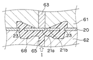
以下に、本発明の発光装置10の製造方法を、図8A〜図8Dを参照しながら説明する。
まず、金属平板に打ち抜き加工を施して、その表面に金属メッキを施してリードフレーム20を作製する。リードフレーム20は、隙間をあけて対向した一対のリード電極21a、21bを有している。通常は、1枚のリードフレーム20に、複数のリード電極21a、21bの対を形成する。
Below, the manufacturing method of the light-emitting
First, the metal flat plate is punched and the surface thereof is plated with metal to produce the
次に、図8Aに示すように、リードフレーム20を上下に分割されたパッケージ成型用のモールド金型61、62の間に配置して、上下のモールド金型61、62で挟み込む。このとき、リード電極21a、21b、及びハンガーリード23の先端を、パッケージ12の形状を有するモールド金型61、62の空洞64の中に配置する。
Next, as shown in FIG. 8A, the
その後、図8Bのように、下側モールド金型62の材料注入ゲート65より、モールド金型61、62の空洞64内へ成形材料68を注入する。上側モールド金型61には、パッケージ12の凹部40に対応する突出部66が形成されている。この突出部66がリード電極21a、21bの上面に接触した状態で成形材料を注入すれば、そのリード電極21a、21bの上面に成形材料が付着せず、パッケージ12の凹部40の底面にリード電極21a、21bを露出させることができる。
Thereafter, as shown in FIG. 8B, the
モールド金型61、62内の成形材料68が硬化したら(図8C)、図8Dに図示しているように、まず下側モールド金型62を外し、次いで上側モールド金型61を外す。上側モールド金型61を外す際には、上側モールド金型61にスライド可能に挿通してある押出しピン63をP方向に押し出せば、上側モールド金型61パッケージ12を取り出しやすい。
When the
図8A〜図8Dに示す一連の工程により、図3のようなリードフレーム20に固定されたパッケージ12が得られる。なお、図3には、パッケージ12が1つだけ図示されているが、通常は1枚のリードフレーム20に複数のパッケージ12が形成される。複数のパッケージ12を製造する場合には、各パッケージにそれぞれ対応する複数の空洞64を備えたモールド金型61、62を使用する。複数の空洞64に同時に成形材料を注入することにより、複数のパッケージ12を同時に形成することができる。
The
リードフレーム20に固定されたパッケージ12に発光素子30等を組み込んで、個々の発光装置10を得るまでの工程を、図1〜図3を参照しながら以下に説明する。
まず、パッケージ12の凹部40内に発光素子30を固定する。凹部40の底面42に露出したリード電極12aの一方に発光素子30をダイボンドする。次いで、発光素子30の正極及び負極と、リード電極21a、21bとを、導電ワイヤ80でワイヤボンディングする。その後、必要に応じて透光性の封止樹脂により凹部40を封止してもよい。また、封止樹脂に、蛍光体やフィラーを混入することもできる。
A process from obtaining the individual
First, the
その後、リード電極21a、21bの外部端子22a、22bを、図3の破線αの位置でリードフレーム20から切り離す。このとき、パッケージ12は、x方向の外面に食い込んだハンガーリード23によって支持されている。そして、外部端子22a、22bを、破線γの位置でパッケージ12の背面15方向(図2のy方向)に折り曲げる。さらに、外部端子22a、22bを、破線βの位置で、実装面16と対向する上面17方向(z方向)に折り曲げて、実装面16の段部52に配置する。その際に、先に破線γに沿って折り曲げた部分は、背面15側の切欠き51に配置されることになる。
Thereafter, the
リード電極21a、21bの外部端子22a、22bの折り曲げ加工が終わったら、最後に、パッケージ12をハンガーリード23から外す。ハンガーリード23の強度はそれほど高くないため、ハンガーリード23は容易に曲げることができ、パッケージ12から簡単に抜去することができる。
When the bending of the
以下に、発光装置10の各構成部材について詳述する。
(発光素子30)
発光素子30には、発光ダイオード等の半導体発光素子が好適である。また、発光素子30は、様々な発光波長のものが使用できる。
Below, each structural member of the light-emitting
(Light emitting element 30)
The
(リード電極21a、21b)
リード電極21a、21bの材料は、導電性であれば特に限定されないが、例えば鉄、銅、鉄入り銅、錫入り銅及び銅、金、銀をメッキしたアルミニウム、鉄、銅等が好適である。
(Lead
The material of the
(パッケージ12)
パッケージ12の成形材料には、例えば、液晶ポリマー、ポリフタルアミド樹脂、ポリブチレンテレフタレート(PBT)などの熱可塑性樹脂を用いることができる。特に、ポリフタルアミド樹脂のような高融点結晶を含有する半結晶性ポリマー樹脂は、表面エネルギーが大きく、パッケージ12の凹部40に充填する封止樹脂との密着性が良好であるので、好適である。これにより、封止樹脂を充填し硬化する工程において、樹脂の冷却過程の間にパッケージと封止樹脂との界面が剥離しにくくなる。また、パッケージ12が発光素子30からの光を効率よく反射できるように、成形部材中に酸化チタンなどの白色顔料などを混合してもよい。
(Package 12)
As the molding material of the
(導電ワイヤ80)
ワイヤボンディング用の導電ワイヤ80としては、例えば、金線、銅線、白金線、アルミニウム線等の金属及びそれらの合金から成るワイヤを用いることが出来る。
(Conductive wire 80)
As the
<実施の形態2>
上述の実施の形態1では、パッケージ12の実装面16に形成した段部52(図2参照)は、リード電極21a、21bの外部端子22a、22bを背面15側に折り曲げた際に、外部端子22a、22bを収納できるように形成されている。よって、外部端子22a、22bがパッケージ12から突出した位置よりも発光面14側には、段部52は形成されていない。
本実施の形態では、外部端子22a、22bがパッケージ12から突出した位置から発光面14側にも、段部52を形成している点で実施の形態1と異なる(図10参照)。それ以外の構成は、実施の形態1と同様である。
<Embodiment 2>
In the first embodiment described above, the stepped portion 52 (see FIG. 2) formed on the mounting
The present embodiment is different from the first embodiment in that a
段部52は、実装面16よりも内方に位置している。そして、リード電極21a、21bは、実装面16の段部52の位置から突出している。すなわち、リード電極21a、21bの外部端子22a、22bと、パッケージ12の外面との境界部分53は、段部52に位置することになる。
The
本発明のように、リード電極21a、21bの挿通されたパッケージ12では、パッケージ12の表面とリード電極21a、21bとの境界において、バリができやすい。そこで、境界部分53を段部52に位置させることにより、境界部分53のバリが実装面16よりも内方に位置させることができる。よって、発光装置10を外部装置に実装するときに、バリが外部装置に接触することがなく、安定した実装が可能になる。
As in the present invention, in the
図1に図示した発光装置10について、中心の輝度分布のシミュレーションを行った。本明細書において『中心の輝度分布』とは、発光面14上で、パッケージ12の長手方向と直交する方向(z方向)におけるパッケージ12の中心位置を通り、パッケージ12の長手方向(x方向)に沿って伸びている線上における輝度の分布のことを指す。
シミュレーションを行った4種類の発光装置10(実施例1〜4)の寸法は表1の通りである。

Table 1 shows the dimensions of the four types of light emitting devices 10 (Examples 1 to 4) on which the simulation was performed.
また、比較のために、発光装置10の2つの傾斜面43が底面42に対して垂直になった比較用の発光装置100(図11参照)を想定して、実施例と同様に中心の輝度分布のシミュレーションも行った。比較例の発光装置100の寸法は表2の通りである。
図12A〜図12Dに、実施例(実線)と比較例(破線)のシミュレーション曲線を示す。各図面には、「x方向における開口部の長さL1」及び「凹部の深さd」が同一である実施例と比較例とを重ねて示している。また、横軸は、x方向におけるパッケージ12の中心位置からのx方向に沿った離間距離を示している。
図12A〜12Dからわかるように、比較例1〜4の発光装置では、光は約4mmの範囲に広がるのみであり、開口部の長さL1全体にわたって広がっていない。これに対して、実施例1〜4の発光装置では、開口部の長さL1のほぼ全体にわたって光が広がっている。よって、本発明の発光装置10は、光が開口部の長手方向に広がって、帯状の発光になることがわかる。
12A to 12D show simulation curves of the example (solid line) and the comparative example (broken line). In each drawing, an example in which “the length L 1 of the opening in the x direction” and “the depth d of the recess” are the same and a comparative example are shown in an overlapping manner. Further, the horizontal axis indicates the separation distance along the x direction from the center position of the
As can be seen from FIG. 12A-12D, the light emitting device of the comparative example 1-4, light is only spread to the range of about 4 mm, not spread over the length L 1 of the opening. In contrast, in the light emitting device of Examples 1 to 4, the light is spread over substantially the entire length L 1 of the opening. Therefore, it can be seen that in the
本発明の発光装置は、液晶ディスプレイのバックライト等のように、極めて薄型の発光部品を必要とする装置に利用可能である。 The light-emitting device of the present invention can be used for devices that require extremely thin light-emitting components, such as a backlight of a liquid crystal display.
10 発光装置、 12 パッケージ、 14 発光面、 15 背面、 16 実装面、 20 リードフレーム、 21a、21b リード電極、 22a、22b リード電極の外部端子、 23 ハンガーリード、 30 発光素子、 40 パッケージの凹部、 41 凹部の開口部、 42 凹部の底面、 43 凹部の傾斜面、 51 切欠き部、 52 段部、 61 上側モールド金型、 62 下側モールド金型、 70 面発光装置、 71 導光板、 72 入射面、 91、92 出射光。 10 light emitting device, 12 package, 14 light emitting surface, 15 back surface, 16 mounting surface, 20 lead frame, 21a, 21b lead electrode, 22a, 22b lead electrode external terminal, 23 hanger lead, 30 light emitting element, 40 package recess, 41 Opening of recess, 42 Bottom surface of recess, 43 Inclined surface of recess, 51 Notch, 52 Step, 61 Upper mold, 62 Lower mold, 70 Surface light emitting device, 71 Light guide plate, 72 Incident Surface, 91, 92 outgoing light.
Claims (7)
前記発光素子と接続された接続用端子と、
前記発光素子を載置する凹部を備え、かつ前記接続用端子の一部を外部に突出させてなるパッケージと、を備えており、
前記凹部の開口部が一方向に長くなっており、
前記凹部の長手方向の両側側壁が凹部の底面から開口部に向って互いに広がる傾斜面を有し、2つの傾斜面を延長したときに該2つの傾斜面のなす角度θが90°以上であり、
前記長手方向の前記開口部の長さL1が、前記長手方向と直交する方向における前記開口部の長さL4の7〜24倍であり、
前記長手方向と直交する方向の前記凹部の両側側壁が前記底面に対して垂直であり、
前記パッケージの外面には、前記開口部が形成された発光面と対向した背面側に切欠き部が形成されており、前記切欠き部に前記接続用端子が配置され、前記接続用端子が前記パッケージの外面より内方に位置し、
前記接続用端子は、前記凹部の前記底面から、前記開口部の長手方向に沿って前記傾斜面の下側まで延在し、そこから前記長手方向と直交し且つ前記発光面と平行な方向に延在して前記パッケージから外部に突出していることを特徴とする発光装置。 A light emitting element;
A connection terminal connected to the light emitting element;
Including a recess for mounting the light emitting element, and a package in which a part of the connection terminal protrudes to the outside.
The opening of the recess is elongated in one direction,
Both side walls in the longitudinal direction of the recess have inclined surfaces that spread from the bottom surface of the recess toward the opening, and an angle θ formed by the two inclined surfaces when the two inclined surfaces are extended is 90 ° or more. ,
The longitudinal the opening length L 1 of a 7 to 24 times the longitudinal direction of the opening in a direction perpendicular length L 4,
Ri der perpendicular to the lateral walls is the bottom surface of the longitudinal direction and direction of the recess perpendicular,
On the outer surface of the package, a notch is formed on the back side facing the light emitting surface on which the opening is formed, the connection terminal is disposed in the notch, and the connection terminal is Located inward from the outer surface of the package,
The connection terminal extends from the bottom surface of the recess to the lower side of the inclined surface along the longitudinal direction of the opening, and from there in a direction perpendicular to the longitudinal direction and parallel to the light emitting surface. extending Mashimashi light emitting device characterized that you have protruding outward from the package.
隣接する発光装置間において、その2つの発光装置から出射される光が重なって前記導光板内に入射されることを特徴とする面発光装置。 In the surface-emitting device including a light guide plate and a plurality of light emitting device, the light emitting device to a light emitting device according to any one of claims 1 to 5, wherein each opening in the incident surface of the light guide plate Arranged in the longitudinal direction to face each other,
A surface light emitting device characterized in that light emitted from the two light emitting devices overlaps and enters the light guide plate between adjacent light emitting devices.
前記パッケージは、前記底面に露出して発光素子に接続し、前記底面と同一面内で前記パッケージを貫通する接続用端子を有し、
前記凹部の開口部が一方向に長くなっており、
前記凹部の長手方向の両側側壁が凹部の底面から開口部に向って互いに広がる傾斜面を有し、2つの傾斜面を延長したときに該2つの傾斜面のなす角度θが90°以上であり、
前記長手方向の前記開口部の長さL1が、前記長手方向と直交する方向における前記開口部の長さL4の7〜24倍であり、
前記長手方向と直交する方向の前記凹部の両側側壁が前記底面に対して垂直であり、
前記パッケージの外面には、前記開口部が形成された発光面と対向した背面側に切欠き部が形成されており、前記切欠き部に前記接続用端子が配置され、前記接続用端子が前記パッケージの外面より内方に位置し、
前記接続用端子は、前記凹部の前記底面から、前記開口部の長手方向に沿って前記傾斜面の下側まで延在し、そこから前記長手方向と直交し且つ前記発光面と平行な方向に延在して前記パッケージから外部に突出していることを特徴とする発光装置用パッケージ。 In a light emitting device package in which a recess having a bottom surface on which a light emitting element is mounted is formed,
The package has a connection terminal that is exposed on the bottom surface and connected to the light emitting element, and penetrates the package in the same plane as the bottom surface,
The opening of the recess is elongated in one direction,
Both side walls in the longitudinal direction of the recess have inclined surfaces that spread from the bottom surface of the recess toward the opening, and an angle θ formed by the two inclined surfaces when the two inclined surfaces are extended is 90 ° or more. ,
The longitudinal the opening length L 1 of a 7 to 24 times the longitudinal direction of the opening in a direction perpendicular length L 4,
Ri der perpendicular to the lateral walls is the bottom surface of the longitudinal direction and direction of the recess perpendicular,
On the outer surface of the package, a notch is formed on the back side facing the light emitting surface on which the opening is formed, the connection terminal is disposed in the notch, and the connection terminal is Located inward from the outer surface of the package,
The connection terminal extends from the bottom surface of the recess to the lower side of the inclined surface along the longitudinal direction of the opening, and from there in a direction perpendicular to the longitudinal direction and parallel to the light emitting surface. the light emitting device package according to claim that you have protruding outward from the package extends.
Priority Applications (3)
| Application Number | Priority Date | Filing Date | Title |
|---|---|---|---|
| JP2007280449A JP5277610B2 (en) | 2007-10-29 | 2007-10-29 | Light emitting device, surface light emitting device, and package for light emitting device |
| US12/259,899 US8759866B2 (en) | 2007-10-29 | 2008-10-28 | Light emitting device |
| US14/276,958 US9465154B2 (en) | 2007-10-29 | 2014-05-13 | Light emitting device |
Applications Claiming Priority (1)
| Application Number | Priority Date | Filing Date | Title |
|---|---|---|---|
| JP2007280449A JP5277610B2 (en) | 2007-10-29 | 2007-10-29 | Light emitting device, surface light emitting device, and package for light emitting device |
Related Child Applications (1)
| Application Number | Title | Priority Date | Filing Date |
|---|---|---|---|
| JP2013107660A Division JP5549759B2 (en) | 2013-05-22 | 2013-05-22 | Light emitting device, surface light emitting device, and package for light emitting device |
Publications (3)
| Publication Number | Publication Date |
|---|---|
| JP2009111068A JP2009111068A (en) | 2009-05-21 |
| JP2009111068A5 JP2009111068A5 (en) | 2010-11-18 |
| JP5277610B2 true JP5277610B2 (en) | 2013-08-28 |
Family
ID=40587209
Family Applications (1)
| Application Number | Title | Priority Date | Filing Date |
|---|---|---|---|
| JP2007280449A Active JP5277610B2 (en) | 2007-10-29 | 2007-10-29 | Light emitting device, surface light emitting device, and package for light emitting device |
Country Status (2)
| Country | Link |
|---|---|
| US (2) | US8759866B2 (en) |
| JP (1) | JP5277610B2 (en) |
Families Citing this family (9)
| Publication number | Priority date | Publication date | Assignee | Title |
|---|---|---|---|---|
| JP5251788B2 (en) * | 2009-08-25 | 2013-07-31 | 豊田合成株式会社 | Side view type light emitting device and manufacturing method thereof |
| MY170920A (en) | 2010-11-02 | 2019-09-17 | Carsem M Sdn Bhd | Leadframe package with recessed cavity for led |
| MY156107A (en) | 2011-11-01 | 2016-01-15 | Carsem M Sdn Bhd | Large panel leadframe |
| JP6078948B2 (en) | 2012-01-20 | 2017-02-15 | 日亜化学工業株式会社 | Package molded body for light emitting device and light emitting device using the same |
| JP6236999B2 (en) * | 2013-08-29 | 2017-11-29 | 日亜化学工業株式会社 | Light emitting device |
| EP3000579B1 (en) * | 2014-09-29 | 2019-04-17 | Nichia Corporation | Method for manufacturing package, method for manufacturing light emitting device, package and light emitting device |
| JP6395045B2 (en) * | 2014-11-18 | 2018-09-26 | 日亜化学工業株式会社 | Composite substrate, light emitting device, and manufacturing method thereof |
| JP6206442B2 (en) * | 2015-04-30 | 2017-10-04 | 日亜化学工業株式会社 | Package, method for manufacturing the same, and light emitting device |
| CN110319375B (en) * | 2018-03-30 | 2022-02-15 | 松下知识产权经营株式会社 | Lighting device |
Family Cites Families (27)
| Publication number | Priority date | Publication date | Assignee | Title |
|---|---|---|---|---|
| DE4242842C2 (en) * | 1992-02-14 | 1999-11-04 | Sharp Kk | Light-emitting component for surface mounting and method for its production |
| JPH0837339A (en) * | 1994-07-21 | 1996-02-06 | Nec Corp | Semiconductor laser diode device of reflection prevention type |
| JP3488570B2 (en) * | 1996-03-29 | 2004-01-19 | ローム株式会社 | LED light emitting device and surface emitting lighting device using the same |
| JP4125848B2 (en) * | 1999-12-17 | 2008-07-30 | ローム株式会社 | Chip type light emitting device with case |
| USD453745S1 (en) * | 1999-12-27 | 2002-02-19 | Nichia Corporation | Light emitting diode |
| USD490782S1 (en) * | 1999-12-27 | 2004-06-01 | Nichia Corporation | Light emitting diode |
| JP4066608B2 (en) * | 2001-03-16 | 2008-03-26 | 日亜化学工業株式会社 | Package molded body and manufacturing method thereof |
| US6874910B2 (en) * | 2001-04-12 | 2005-04-05 | Matsushita Electric Works, Ltd. | Light source device using LED, and method of producing same |
| JP3991961B2 (en) | 2002-09-05 | 2007-10-17 | 日亜化学工業株式会社 | Side-emitting type light emitting device |
| TWI292961B (en) * | 2002-09-05 | 2008-01-21 | Nichia Corp | Semiconductor device and an optical device using the semiconductor device |
| JP4144498B2 (en) * | 2002-10-01 | 2008-09-03 | 松下電器産業株式会社 | Linear light source device, method for manufacturing the same, and surface light emitting device |
| US6835960B2 (en) * | 2003-03-03 | 2004-12-28 | Opto Tech Corporation | Light emitting diode package structure |
| CN100466308C (en) * | 2003-09-29 | 2009-03-04 | 松下电器产业株式会社 | Linear light source and production method therefor and surface emission device |
| JP2005252168A (en) * | 2004-03-08 | 2005-09-15 | Nichia Chem Ind Ltd | Surface mount light emitting device |
| DE102004021175B4 (en) * | 2004-04-30 | 2023-06-29 | OSRAM Opto Semiconductors Gesellschaft mit beschränkter Haftung | Semiconductor chips for optoelectronics and methods for their manufacture |
| JP2006108333A (en) * | 2004-10-04 | 2006-04-20 | Toyoda Gosei Co Ltd | Lamp |
| JP4830321B2 (en) * | 2005-03-14 | 2011-12-07 | パナソニック株式会社 | Semiconductor light emitting device |
| JP2006253550A (en) * | 2005-03-14 | 2006-09-21 | Matsushita Electric Ind Co Ltd | Manufacturing method of linear light source device |
| JP2006286348A (en) * | 2005-03-31 | 2006-10-19 | Minebea Co Ltd | Planar lighting system |
| JP2006351773A (en) * | 2005-06-15 | 2006-12-28 | Rohm Co Ltd | Semiconductor light-emitting apparatus |
| WO2007004450A1 (en) * | 2005-07-04 | 2007-01-11 | Matsushita Electric Industrial Co., Ltd. | Linear light source device, planar light emitting device and liquid crystal display device |
| KR100649679B1 (en) * | 2005-07-19 | 2006-11-27 | 삼성전기주식회사 | Side emitting led package and blu using the same |
| EP1919002B1 (en) * | 2005-08-23 | 2018-07-18 | Kabushiki Kaisha Toshiba | Light-emitting device, backlight using same, and liquid crystal display |
| JP2007116107A (en) * | 2005-09-22 | 2007-05-10 | Toshiba Lighting & Technology Corp | Light emitting device |
| USD566664S1 (en) * | 2006-09-08 | 2008-04-15 | Lg Innotek Co., Ltd. | Light-emitting diode (LED) |
| KR100981214B1 (en) * | 2008-01-28 | 2010-09-10 | 알티전자 주식회사 | Light emitting diode package |
| US9147812B2 (en) * | 2008-06-24 | 2015-09-29 | Cree, Inc. | Methods of assembly for a semiconductor light emitting device package |
-
2007
- 2007-10-29 JP JP2007280449A patent/JP5277610B2/en active Active
-
2008
- 2008-10-28 US US12/259,899 patent/US8759866B2/en active Active
-
2014
- 2014-05-13 US US14/276,958 patent/US9465154B2/en active Active
Also Published As
| Publication number | Publication date |
|---|---|
| US20090114936A1 (en) | 2009-05-07 |
| US8759866B2 (en) | 2014-06-24 |
| JP2009111068A (en) | 2009-05-21 |
| US20140247621A1 (en) | 2014-09-04 |
| US9465154B2 (en) | 2016-10-11 |
Similar Documents
| Publication | Publication Date | Title |
|---|---|---|
| JP5277610B2 (en) | Light emitting device, surface light emitting device, and package for light emitting device | |
| JP4857791B2 (en) | Manufacturing method of semiconductor device | |
| KR100526546B1 (en) | LED Device and Manufacturing Method Thereof | |
| KR101635650B1 (en) | Light emitting device | |
| JP4952233B2 (en) | Semiconductor device | |
| KR101096423B1 (en) | Light emitting device | |
| CN110076953B (en) | Method for manufacturing package, method for manufacturing light emitting device, package, and light emitting device | |
| JP2017224852A (en) | Light-emitting device | |
| JP2019062237A (en) | Side emission light emitting device | |
| JP2007207986A5 (en) | ||
| KR101455431B1 (en) | Light emitting device | |
| KR20110103929A (en) | Light emitting diode package and light unit having the same | |
| KR102161069B1 (en) | Light emitting device | |
| JP2009302241A (en) | Method for manufacturing resin seal, method for manufacturing board for packaging led chip, metal mold of the board for packaging the led chip, the board for packaging the led chip and led | |
| JP2008010562A (en) | Light source device and plane lighting apparatus | |
| JP5549759B2 (en) | Light emitting device, surface light emitting device, and package for light emitting device | |
| JP5180690B2 (en) | LED chip mounting substrate manufacturing method, LED chip mounting substrate mold, LED chip mounting substrate, and LED | |
| KR20080062504A (en) | A method for fabricating side-view light emitting diode package | |
| JP2017117901A (en) | Light-emitting device, and package and manufacturing method thereof | |
| KR100877550B1 (en) | Light-emitting diode package for light-emitting diode lead panel | |
| US10763414B2 (en) | Semiconductor light-emitting device | |
| JP2018006453A (en) | Light-emitting device, manufacturing method of the same, and manufacturing method of package | |
| WO2009145056A1 (en) | Reflection light emitting diode | |
| WO2012046701A1 (en) | Light emitting device, light emitting module, and planar light source device | |
| KR101311351B1 (en) | Light emitting device package |
Legal Events
| Date | Code | Title | Description |
|---|---|---|---|
| A521 | Request for written amendment filed |
Free format text: JAPANESE INTERMEDIATE CODE: A523 Effective date: 20101004 |
|
| A621 | Written request for application examination |
Free format text: JAPANESE INTERMEDIATE CODE: A621 Effective date: 20101004 |
|
| A131 | Notification of reasons for refusal |
Free format text: JAPANESE INTERMEDIATE CODE: A131 Effective date: 20120424 |
|
| A977 | Report on retrieval |
Free format text: JAPANESE INTERMEDIATE CODE: A971007 Effective date: 20120425 |
|
| A521 | Request for written amendment filed |
Free format text: JAPANESE INTERMEDIATE CODE: A523 Effective date: 20120622 |
|
| A131 | Notification of reasons for refusal |
Free format text: JAPANESE INTERMEDIATE CODE: A131 Effective date: 20130108 |
|
| A521 | Request for written amendment filed |
Free format text: JAPANESE INTERMEDIATE CODE: A523 Effective date: 20130311 |
|
| TRDD | Decision of grant or rejection written | ||
| A01 | Written decision to grant a patent or to grant a registration (utility model) |
Free format text: JAPANESE INTERMEDIATE CODE: A01 Effective date: 20130423 |
|
| A61 | First payment of annual fees (during grant procedure) |
Free format text: JAPANESE INTERMEDIATE CODE: A61 Effective date: 20130506 |
|
| R150 | Certificate of patent or registration of utility model |
Ref document number: 5277610 Country of ref document: JP Free format text: JAPANESE INTERMEDIATE CODE: R150 Free format text: JAPANESE INTERMEDIATE CODE: R150 |
|
| R250 | Receipt of annual fees |
Free format text: JAPANESE INTERMEDIATE CODE: R250 |
|
| R250 | Receipt of annual fees |
Free format text: JAPANESE INTERMEDIATE CODE: R250 |
|
| R250 | Receipt of annual fees |
Free format text: JAPANESE INTERMEDIATE CODE: R250 |
|
| R250 | Receipt of annual fees |
Free format text: JAPANESE INTERMEDIATE CODE: R250 |
|
| R250 | Receipt of annual fees |
Free format text: JAPANESE INTERMEDIATE CODE: R250 |
|
| R250 | Receipt of annual fees |
Free format text: JAPANESE INTERMEDIATE CODE: R250 |
|
| R250 | Receipt of annual fees |
Free format text: JAPANESE INTERMEDIATE CODE: R250 |