JP6236999B2 - Light emitting device - Google Patents
Light emitting device Download PDFInfo
- Publication number
- JP6236999B2 JP6236999B2 JP2013177773A JP2013177773A JP6236999B2 JP 6236999 B2 JP6236999 B2 JP 6236999B2 JP 2013177773 A JP2013177773 A JP 2013177773A JP 2013177773 A JP2013177773 A JP 2013177773A JP 6236999 B2 JP6236999 B2 JP 6236999B2
- Authority
- JP
- Japan
- Prior art keywords
- light emitting
- emitting element
- light
- lead
- emitting device
- Prior art date
- Legal status (The legal status is an assumption and is not a legal conclusion. Google has not performed a legal analysis and makes no representation as to the accuracy of the status listed.)
- Active
Links
Images


Classifications
-
- H—ELECTRICITY
- H01—ELECTRIC ELEMENTS
- H01L—SEMICONDUCTOR DEVICES NOT COVERED BY CLASS H10
- H01L33/00—Semiconductor devices with at least one potential-jump barrier or surface barrier specially adapted for light emission; Processes or apparatus specially adapted for the manufacture or treatment thereof or of parts thereof; Details thereof
- H01L33/48—Semiconductor devices with at least one potential-jump barrier or surface barrier specially adapted for light emission; Processes or apparatus specially adapted for the manufacture or treatment thereof or of parts thereof; Details thereof characterised by the semiconductor body packages
- H01L33/58—Optical field-shaping elements
- H01L33/60—Reflective elements
-
- H—ELECTRICITY
- H01—ELECTRIC ELEMENTS
- H01L—SEMICONDUCTOR DEVICES NOT COVERED BY CLASS H10
- H01L24/00—Arrangements for connecting or disconnecting semiconductor or solid-state bodies; Methods or apparatus related thereto
- H01L24/93—Batch processes
- H01L24/95—Batch processes at chip-level, i.e. with connecting carried out on a plurality of singulated devices, i.e. on diced chips
- H01L24/97—Batch processes at chip-level, i.e. with connecting carried out on a plurality of singulated devices, i.e. on diced chips the devices being connected to a common substrate, e.g. interposer, said common substrate being separable into individual assemblies after connecting
-
- H—ELECTRICITY
- H01—ELECTRIC ELEMENTS
- H01L—SEMICONDUCTOR DEVICES NOT COVERED BY CLASS H10
- H01L33/00—Semiconductor devices with at least one potential-jump barrier or surface barrier specially adapted for light emission; Processes or apparatus specially adapted for the manufacture or treatment thereof or of parts thereof; Details thereof
- H01L33/48—Semiconductor devices with at least one potential-jump barrier or surface barrier specially adapted for light emission; Processes or apparatus specially adapted for the manufacture or treatment thereof or of parts thereof; Details thereof characterised by the semiconductor body packages
- H01L33/50—Wavelength conversion elements
- H01L33/501—Wavelength conversion elements characterised by the materials, e.g. binder
- H01L33/502—Wavelength conversion materials
-
- H—ELECTRICITY
- H01—ELECTRIC ELEMENTS
- H01L—SEMICONDUCTOR DEVICES NOT COVERED BY CLASS H10
- H01L33/00—Semiconductor devices with at least one potential-jump barrier or surface barrier specially adapted for light emission; Processes or apparatus specially adapted for the manufacture or treatment thereof or of parts thereof; Details thereof
- H01L33/48—Semiconductor devices with at least one potential-jump barrier or surface barrier specially adapted for light emission; Processes or apparatus specially adapted for the manufacture or treatment thereof or of parts thereof; Details thereof characterised by the semiconductor body packages
- H01L33/50—Wavelength conversion elements
- H01L33/505—Wavelength conversion elements characterised by the shape, e.g. plate or foil
-
- H—ELECTRICITY
- H01—ELECTRIC ELEMENTS
- H01L—SEMICONDUCTOR DEVICES NOT COVERED BY CLASS H10
- H01L33/00—Semiconductor devices with at least one potential-jump barrier or surface barrier specially adapted for light emission; Processes or apparatus specially adapted for the manufacture or treatment thereof or of parts thereof; Details thereof
- H01L33/48—Semiconductor devices with at least one potential-jump barrier or surface barrier specially adapted for light emission; Processes or apparatus specially adapted for the manufacture or treatment thereof or of parts thereof; Details thereof characterised by the semiconductor body packages
- H01L33/52—Encapsulations
- H01L33/54—Encapsulations having a particular shape
-
- H—ELECTRICITY
- H01—ELECTRIC ELEMENTS
- H01L—SEMICONDUCTOR DEVICES NOT COVERED BY CLASS H10
- H01L33/00—Semiconductor devices with at least one potential-jump barrier or surface barrier specially adapted for light emission; Processes or apparatus specially adapted for the manufacture or treatment thereof or of parts thereof; Details thereof
- H01L33/48—Semiconductor devices with at least one potential-jump barrier or surface barrier specially adapted for light emission; Processes or apparatus specially adapted for the manufacture or treatment thereof or of parts thereof; Details thereof characterised by the semiconductor body packages
- H01L33/62—Arrangements for conducting electric current to or from the semiconductor body, e.g. lead-frames, wire-bonds or solder balls
-
- H—ELECTRICITY
- H01—ELECTRIC ELEMENTS
- H01L—SEMICONDUCTOR DEVICES NOT COVERED BY CLASS H10
- H01L2224/00—Indexing scheme for arrangements for connecting or disconnecting semiconductor or solid-state bodies and methods related thereto as covered by H01L24/00
- H01L2224/73—Means for bonding being of different types provided for in two or more of groups H01L2224/10, H01L2224/18, H01L2224/26, H01L2224/34, H01L2224/42, H01L2224/50, H01L2224/63, H01L2224/71
- H01L2224/732—Location after the connecting process
- H01L2224/73251—Location after the connecting process on different surfaces
- H01L2224/73253—Bump and layer connectors
-
- H—ELECTRICITY
- H01—ELECTRIC ELEMENTS
- H01L—SEMICONDUCTOR DEVICES NOT COVERED BY CLASS H10
- H01L2924/00—Indexing scheme for arrangements or methods for connecting or disconnecting semiconductor or solid-state bodies as covered by H01L24/00
- H01L2924/10—Details of semiconductor or other solid state devices to be connected
- H01L2924/11—Device type
- H01L2924/12—Passive devices, e.g. 2 terminal devices
- H01L2924/1204—Optical Diode
- H01L2924/12041—LED
-
- H—ELECTRICITY
- H01—ELECTRIC ELEMENTS
- H01L—SEMICONDUCTOR DEVICES NOT COVERED BY CLASS H10
- H01L2924/00—Indexing scheme for arrangements or methods for connecting or disconnecting semiconductor or solid-state bodies as covered by H01L24/00
- H01L2924/15—Details of package parts other than the semiconductor or other solid state devices to be connected
- H01L2924/151—Die mounting substrate
- H01L2924/156—Material
- H01L2924/15786—Material with a principal constituent of the material being a non metallic, non metalloid inorganic material
- H01L2924/15788—Glasses, e.g. amorphous oxides, nitrides or fluorides
-
- H—ELECTRICITY
- H01—ELECTRIC ELEMENTS
- H01L—SEMICONDUCTOR DEVICES NOT COVERED BY CLASS H10
- H01L33/00—Semiconductor devices with at least one potential-jump barrier or surface barrier specially adapted for light emission; Processes or apparatus specially adapted for the manufacture or treatment thereof or of parts thereof; Details thereof
- H01L33/48—Semiconductor devices with at least one potential-jump barrier or surface barrier specially adapted for light emission; Processes or apparatus specially adapted for the manufacture or treatment thereof or of parts thereof; Details thereof characterised by the semiconductor body packages
- H01L33/483—Containers
- H01L33/486—Containers adapted for surface mounting
Description
本発明は、発光装置に関する。 The present invention relates to a light emitting device.
画像表示装置のバックライト光源の用途に、発光ダイオードを用いた発光装置が広く用いられている。画像表示装置のバックライト用の発光装置は、例えば、導光板と導光板の側面に設けられた発光装置とを含んでなり、発光装置が出射する光が導光板の発光面から出射されるように構成される。また、携帯端末用の画像表示装置に用いられるバックライト用の発光装置としては、例えば、特許文献1に開示されているような、実装面と発光面とが直交し、その側面が光取り出し面となったサイドビュー型(側面発光型)発光装置が広く用いられている。この携帯端末用の画像表示装置に用いられるバックライト光源用の発光装置には、発光素子の光を効率よく前方の取り出すことができこと及び小型で軽量であることに加え、薄型であることが求められる。
A light emitting device using a light emitting diode is widely used for a backlight light source of an image display device. A light emitting device for a backlight of an image display device includes, for example, a light guide plate and a light emitting device provided on a side surface of the light guide plate so that light emitted from the light emitting device is emitted from the light emitting surface of the light guide plate. Configured. In addition, as a light emitting device for a backlight used for an image display device for a portable terminal, for example, as disclosed in
しかしながら、携帯端末が薄型になるにしたがって、より薄いサイドビュー型の発光装置が求められているが、従来のサイドビュー型の発光装置では十分にその薄型化の要求に応えられていなかった。 However, as the portable terminal becomes thinner, a thinner side-view type light emitting device is required. However, the conventional side-view type light emitting device has not sufficiently met the demand for thickness reduction.
そこで、本発明は、発光素子の光を効率よく前方に取り出すことができ、小型でかつ薄型のサイドビュー型の発光装置を提供することを目的とする。 In view of the above, an object of the present invention is to provide a small and thin side-view type light-emitting device that can efficiently extract light from a light-emitting element forward.
以上の目的を達成するために、本発明に係る発光装置は、上面と下面と前面とを有し、前記前面に前記上面から前記下面にわたって凹部が溝状に形成された樹脂成形体と、前記樹脂成形体に埋設されたリードとを備えた基体と、
発光素子チップと前記発光素子チップから出射される光を透過する透光性部材と発光領域を所定の範囲に制限する反射層を側面に有する発光素子とを備え、
前記発光素子は、前記凹部の底面に設けられていることを特徴とする。
In order to achieve the above object, a light emitting device according to the present invention has an upper surface, a lower surface, and a front surface, and a resin molded body in which a recess is formed in a groove shape from the upper surface to the lower surface on the front surface, A base including a lead embedded in the resin molded body;
A light-emitting element chip, a translucent member that transmits light emitted from the light-emitting element chip, and a light-emitting element having a reflective layer on a side surface that limits a light-emitting region to a predetermined range,
The light emitting element is provided on a bottom surface of the recess.
以上のように構成された本発明に係る発光装置によれば、発光素子の光を効率よく前方に取り出すことができ、小型でかつ薄型のサイドビュー型の発光装置を提供することができる。 According to the light emitting device according to the present invention configured as described above, the light of the light emitting element can be efficiently extracted forward, and a small and thin side view type light emitting device can be provided.
以下、図面を参照しながら本発明に係る実施形態の発光装置について説明する。
図1は、本発明に係る実施形態の発光装置の構成を示す斜視図であり、図2は、実施形態の基体20の構成を示す斜視図であり、実装面側となる第1面23aを上にして示している。
図1に示すように、実施形態の発光装置は、凹部24を備えた基体20と、基体20の凹部底面24bに設けられた発光素子10とを含む。
Hereinafter, a light emitting device according to an embodiment of the present invention will be described with reference to the drawings.
FIG. 1 is a perspective view illustrating a configuration of a light emitting device according to an embodiment of the present invention, and FIG. 2 is a perspective view illustrating a configuration of a
As shown in FIG. 1, the light emitting device of the embodiment includes a
基体20
基体20は、樹脂成形体23と、樹脂成形体23に埋設された第1リード21と第2リード22とを含む。
The
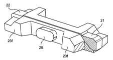
樹脂成形体23は、対向する2つの主面の一方の面である第1面23aと、対向する2つの主面の他方の面である第2面23bと、前面23cと、背面23fと、第1端面23dと、第2端面23eとを有し、前面23cに溝状の凹部24を有する。尚、上述したように、図1等では、実装面となる第1面23aを上にして示しているので、実装状態では、第1面23aが下面であり、第2面23bが上面である。凹部24は、前面23cに第1面23aから第2面23bにわたって貫通するように形成されており、凹部底面24bと2つの側壁24aとを有する。凹部の側壁24aは、凹部底面24bより開口側が広くなるように傾斜していることが好ましく、開口側を広くすることにより、発光素子を容易に実装することができる。
The resin molded
樹脂成形体23において、第1面23aは、第1端面23d側及び第2端面23e側にそれぞれ段差が形成されており、その段差の部分で樹脂成形体23の厚さが薄くなっている。尚、第1面23aにおいて、第1端面23d側及び第2端面23e側の段差を構成する傾斜面23acとそれに連続する平坦面23abを除いた部分を載置面23asという。
樹脂成形体23の成形材料としては、例えば、熱可塑性樹脂、熱硬化性樹脂等、具体的には、ポリフタルアミド(PPA)、ポリカーボネート樹脂、ポリフェニレンサルファイド(PPS)、液晶ポリマー(LCP)、ABS樹脂、エポキシ樹脂、フェノール樹脂、アクリル樹脂、PBT樹脂等の樹脂等が挙げられる。好適には、熱可塑性樹脂を用いる。また、成形材料中に酸化チタンなどの光反射性物質などを混合して、樹脂成形体の表面における光の反射率を高めることもできる。これにより、戻り光を効率的に反射することができる。
In the resin molded
The molding material of the
第1リード21は、図3に示すように、一端面21eと他端面21fとを有し、一端面21eから他端面21fに至る方向に長い柱形状の略6面体であり、一端面21eと他端面21fの間に4つの側面21a,21b,21c,21dを有する。図3には、第1リード21と第2リード22とを、樹脂成形体23内部における位置関係を保った状態で示している。また、図3におけるハッチングは、第1リード21と第2リード22の樹脂成形体23から露出される部分を示しており、断面を示すものではない。
As shown in FIG. 3, the
第1リード21は、一端面21eが樹脂成形体23の第1端面23dの中央部から露出し、側面21bの一端面21e側の一部が樹脂成形体23の第1面23aの傾斜面23ac及び平坦面23abから露出されるように樹脂成形体23に埋設される。第1リード21の側面21aの他端面21f側の一部が樹脂成形体23の凹部底面24bから露出される。尚、第1リード21の側面21cには凹部21gが設けられており、その凹部によって第1リード21が樹脂成形体23から抜けるのを防止している。
As for the 1st lead | read |
第2リード22は、図3に示すように、一端面22eと他端面22fとを有し、一端面22eから他端面22fに至る方向に長い柱形状の略6面体であり、一端面22eと他端面22fの間に4つの側面22a,22b,22c,22dを有する。
As shown in FIG. 3, the
第2リード22は、図1に示すように、一端面22eが樹脂成形体23の第2端面23eの中央部から露出し、側面22bの一端面22e側の一部が樹脂成形体23の第1面23aの傾斜面23ac及び平坦面23abから露出されるように樹脂成形体23に埋設される。第2リード22の側面22aの他端面22f側の一部が樹脂成形体23の凹部底面24bから露出される。尚、第2リード22の側面22cには凹部22gが設けられており、その凹部によって第2リード22が樹脂成形体23から抜けるのを防止している。
尚、本実施形態の発光装置では、第1リード21を、側面21bの一端面21e側の一部が樹脂成形体23から露出されるように樹脂成形体23に埋設し、第2リード22を、側面22bの一端面22e側の一部が樹脂成形体23から露出されるように樹脂成形体23に埋設した。しかしながら、本発明はこれに限定されるものではなく、例えば、他端面21f側の側面21b及び他端面22f側の側面22bが、載置面23asと同一平面上に位置して露出するように、第1リード21及び第2リード22を樹脂成形体23に埋設してもよいし、他端面21f側の側面21b及び他端面22f側の側面22bが、載置面23asより突出して露出するように第1リード21及び第2リード22を樹脂成形体23に埋設してもよい。
As shown in FIG. 1, one
In the light emitting device of this embodiment, the
図3に示すように、本発明では、第1リード21及び第2リード22をそれぞれ、一方向に長い柱形状の略6面体とし、4つの側面のうちの1つの側面21a,22aの他端面21f,22f側の一部を凹部底面24bに露出させ、側面21a,22aに直交する側面21b,22bの一端面21e,22e側の一部を外部回路と接続するための主要な外部接続面としている。このように、本発明では、第1リード21及び第2リード22をそれぞれ、柱形状の略6面体とすることにより、直交する2つの側面の一方を発光素子10との接続に用い、他方を外部接続面として用いることを可能とし、さらに、放熱特性を向上させている。
第1リードおよび第2リードは、例えば、アルミニウム、鉄、ニッケル、銅、銅合金、ステンレス鋼、インバー合金を含む鉄合金などのいずれか1つ以上からなる導電性材料を用いて構成することができる。異種の金属をクラッドしたクラッド材を用いてもよい。また、リードフレームは、表面を金、銀、ニッケル、パラジウムおよびそれらの合金などでメッキすることが好ましい。
また、リードフレームの厚みは、例えば、50μm〜1000μmであり、好ましくは、100μm〜500μmとする。また、リードフレームは、目的に応じて厚みを変化させることができる。このリードフレームの厚みは、エッチング(ハーフエッチング)又はプレス加工により変化させることも可能である。
As shown in FIG. 3, in the present invention, each of the
For example, the first lead and the second lead may be configured using a conductive material made of any one or more of aluminum, iron, nickel, copper, copper alloy, stainless steel, iron alloy including Invar alloy, and the like. it can. A clad material clad with a dissimilar metal may be used. The lead frame is preferably plated with gold, silver, nickel, palladium, and alloys thereof.
The lead frame has a thickness of, for example, 50 μm to 1000 μm, and preferably 100 μm to 500 μm. The lead frame can be changed in thickness according to the purpose. The thickness of the lead frame can be changed by etching (half etching) or pressing.
以上のように構成された基体20は、例えば、以下のようにして作製することができる。
まず、樹脂成形体23の形状に対応するキャビティを形成する金型を準備し、そのキャビティ内に、それぞれ第1リード21と第2リード22となる2つの柱状リードを端部が所定の間隔になるように配置して固定する。尚、柱状リードの所定の間隔になるように配置された端部はそれぞれ、図3に示す他端面21fと他端面22fとに対応する。
The
First, a mold for forming a cavity corresponding to the shape of the resin molded
例えば、この金型は、分離可能な2つ以上の金型からなり、1つの金型に凹部24に対応して凸部が設けられ、他の1つの金型に、樹脂を注入するためのゲートが形成されている。
For example, this mold is composed of two or more separable molds, and one mold is provided with a convex portion corresponding to the
次に、第1リード21と第2リード22とが固定されたキャビティ内に樹脂を注入して硬化する。
Next, resin is injected into the cavity in which the
樹脂を硬化した後、金型から取り出して、樹脂成形体23の外側に延びた柱状リードを切断する。
柱状の第1及び第2リード21,22は、一端面21e側及び一端面22e側が所定の長さだけ樹脂成形体23から突出するように第1端面23d及び第2端面23eに沿って(平行に)切断される。以上のようにしてそれぞれ切断面からなる一端面21e,22eが形成される。この切断面からなる一端面21eは、4つの側面21a,21b,21c,21dに直交していることが好ましく、切断面からなる一端面22eは、4つの側面22a,22b,22c,22dに直交していることが好ましい。
尚、図4において、28を付して示す部分は樹脂成形体23におけるゲート跡である。
After the resin is cured, it is taken out from the mold and the columnar leads extending outside the resin molded
The columnar first and second leads 21 and 22 extend along the
In FIG. 4, a portion indicated by 28 is a gate mark in the resin molded
以上のように構成された基体20は、発光素子を収容する凹部24が、第1面23aから第2面23bに貫通するように形成されており、第1面23a側及び第2面23b側には壁(以下、上下の壁という。)がないので、厚さ(第1面23aと第2面23bの間の距離)を薄くできる。
The
しかしながら、凹部24に上下の壁がないことから、第1面23a側及び第2面23b側から発光素子の光が漏れるおそれがあり、発光素子の発光を効率よく前方に取り出すことができない。
However, since the
そこで、本発明では、側面に反射層が形成された発光素子を用いるようにすることで、発光素子の光を効率よく前方の取り出すことができ、かつ薄型の発光装置を実現している。 Therefore, in the present invention, by using a light-emitting element having a reflective layer formed on the side surface, light from the light-emitting element can be efficiently extracted forward, and a thin light-emitting device is realized.
発光素子10
発光素子10は、例えば、発光素子チップ11と発光素子チップ11のチップ発光面上に設けられた透光性部材12と発光素子チップ11と透光性部材12の外周を囲む反射層13とを含む。発光素子10は、正電極3aと負電極3bが形成された発光素子チップ11のチップ実装面と透光性部材12の上面と、該上面及びチップ実装面と直交する側面とからなる四角柱体の側面が反射層13によって覆われてなり、反射層13を含む外形形状も四角柱体となっている。以下、反射層13を除く四角柱体を内側四角柱体といい、反射層13を除く四角柱体を外側四角柱体という。尚、本発明において、発光素子10は四角柱体に限定されるものではないが、発光素子10が四角柱体であると発光素子10の作製が容易となる。以下、発光素子10の製造方法の一例を示す。
The
(発光素子チップ準備)
まず、同一の面側に正電極3aと負電極3bとを備えた発光素子チップ11を準備する。
発光素子チップ11は、半導体から成る発光層を備えたものであれば良い。特に窒化物半導体から成る発光層、中でも窒化ガリウム系化合物半導体(特にInGaN)から成る発光層を備えた発光素子であれば、可視光域の短波長域や近紫外域で強い発光が可能であるため、蛍光体と好適に組み合わせることができる。発光素子チップ11は、発光層から出力される出射光の発光ピーク波長が近紫外線から可視光の短波長領域である240nm〜500nm付近、好ましくは380nm〜420nm、さらに好ましくは450nm〜470nmにある発光スペクトルを有することが望ましい。この波長域で発光をする発光素子であれば、種々の蛍光体との組合せにより、所望の色、特に白色光の発光が可能となる。尚、発光素子10は、ZnSe系、InGaAs系、AlInGaP系などの半導体から成る発光層を有するものでも良い。
(Light emitting element chip preparation)
First, a light emitting
The light emitting
(透光性部材準備)
また、透光性基板1と透光性基板1の一方の面に形成された波長変換層2とを備えた透光性部材12を準備する。
具体的には、透光性基板上に波長変換部材を配置して、例えば、発光素子チップ11と同じ大きさに切断する。
透光性基板1としては、例えば、石英やホウケイ酸硝子等からなるガラス基板が用いられる。透光性基板1の厚みは30μm〜1mmが好ましく、より好ましくは、50〜500μmである。
波長変換層2としては、バインダー樹脂に後述の蛍光体を含有させたものを使用することができる。
(Translucent material preparation)
Moreover, the
Specifically, the wavelength conversion member is disposed on the translucent substrate and cut into the same size as the light emitting
As the
As the
蛍光体は、発光素子チップ11の発光により励起される蛍光体が選択されるが、例えば、発光素子チップ11が青色発光素子であり、白色の発光装置を構成したい場合には、青色で励起されて黄色のブロードな発光を示す蛍光体を用いることが好ましい。このような蛍光体として、例えば、セリウムで付活されたガーネット構造を持つ蛍光体(特に、セリウムで付活され、アルミニウムを含みガーネット構造を持つ蛍光体)が挙げられる。セリウムで付活された蛍光体は、黄色にブロードは発光を示すため、青色発光との組合せによって演色性の良い白色を実現できる。また、ガーネット構造、特にアルミニウムを含むガーネット構造の蛍光体は、熱、光、水分に強く、高輝度な黄色発光を長時間維持することができる。例えば、蛍光体として、(Re1-xSmx)3(Al1-yGay)5O12:Ce(0≦x<1、0≦y≦1、但し、Reは、Y、Gd、La、Lu、Tbからなる群より選択される少なくとも一種の元素である。)で表されるYAG系蛍光体(一般にYAGと略記される)を用いることが好ましい。また、黄色蛍光体の他に、Si6−ZAlZOZN8−Z:Eu、Lu3Al5O12:Ce、BaMgAl10O17:Eu、BaMgAl10O17:Eu,Mn、(Zn,Cd)Zn:Cu、(Sr,Ca)10(PO4)6Cl2:Eu,Mn、(Sr,Ca)2Si5N8:Eu、CaAlSiBxN3+x:Eu、K2SiF6:Mn及びCaAlSiN3:Euなどの蛍光体を用いて照明用光源としての演色性や、バックライト用途としての色再現性を調整することもできる。また、量子ドット蛍光体を用いてもよい。
As the phosphor, a phosphor that is excited by light emission of the light emitting
また、特に発光素子チップ11の発光波長が短波長である場合などは、波長変換層2が2種類以上の蛍光体を含んでいても良い。発光素子チップ11からの1次光によって1種類目の蛍光体を励起、発光させ、その蛍光体の発する2次光によって別の種類の蛍光体を励起、発光させることもできる。また、色度の異なる2種類の蛍光体を用いれば、2種類の蛍光体の量を調整することにより、色度図上において2種類の蛍光体と発光素子の色度点を結んでできる領域内の任意の色度点に対応する発光を得ることができる。
In particular, when the emission wavelength of the light emitting
バインダー樹脂は、例えば、シリコーン樹脂、変性シリコーン樹脂等を使用することが好ましい。また、エポキシ樹脂、変性エポキシ樹脂、アクリル樹脂等の透光性を有する絶縁樹脂を用いることができる。また、これらの樹脂を少なくとも一種以上含むハイブリッド樹脂等、耐候性に優れた樹脂も利用できる。
波長変換層2を形成する方法は、例えば、印刷法、スプレー塗布、圧縮成形、スピンコート、ディスペンス等公知の方法が挙げられる。
波長変換層2は、均一な膜厚でかつ蛍光体粒子が偏在することなく形成することが好ましく、上記列挙した蛍光体層形成方法のなかでは特に印刷法、スプレー塗布又は圧縮成形を用いることが好ましい。
As the binder resin, for example, a silicone resin, a modified silicone resin or the like is preferably used. Alternatively, a light-transmitting insulating resin such as an epoxy resin, a modified epoxy resin, or an acrylic resin can be used. Also, a resin excellent in weather resistance such as a hybrid resin containing at least one of these resins can be used.
Examples of the method for forming the
The
(発光素子チップ配列工程)
次に、図5(a)に示すように、シート6の上に正電極3aと負電極3bが形成された面を下にして発光素子チップ11を所定の間隔で縦横マトリクス状に配列する。ここで、発光素子チップ11を配列する所定の間隔は、反射層13の厚さtを考慮して設定される。具体的には、反射層13の厚さtの2倍に後述の切断幅を加えた間隔に設定される。また、シート6は、例えば一方の面に接着層又は粘着層などが形成されており、その接着層又は粘着層により発光素子チップ11が所定の間隔に保持される。
(Light emitting element chip arrangement process)
Next, as shown in FIG. 5A, the light-emitting element chips 11 are arranged in a vertical and horizontal matrix at predetermined intervals with the surface on which the
(透光性部材接合工程)
次に、図5(b)に示すように、波長変換層2を備えた透光性部材12を発光素子チップ11の上に接着部材4により接合する。
透光性基板1は、例えば、発光素子チップ11と同一または一回り大きい平面形状になるように作製されており、波長変換層2が発光素子チップ11に、例えば、シリコーン樹脂からなる接着部材4を介して接合される。以上の工程により、シート6の上に、それぞれ発光素子チップ11と透光性部材12とを含む複数の内側四角柱体が配列された状態となる。
(Translucent member joining process)
Next, as shown in FIG. 5B, the
The
(樹脂充填工程)
次に、図5(c)に示すように、反射層13を構成する樹脂5を、配列された内側四角柱体の間に樹脂5が充填されるように塗布する。
樹脂5には、光反射性物質を含有させる。このようにすると発光素子チップ11の側面から出射された光を樹脂5に含まれる光反射性物質により波長変換層2の方向に反射させて、発光効率を向上させることができる。光反射性物質としては、TiO2、ZrO2、Nb2O5、Al2O3、MgF、AlN、SiO2、MgOよりなる群から選択される少なくとも1種を用いることができる。
(Resin filling process)
Next, as shown in FIG. 5C, the
The
光反射性物質を含む樹脂5は、例えば、樹脂5を塗布してスキージで押し広げて配列された発光素子チップ11間に樹脂5を充填する。この時、スキージは透光性基板1の透光性部材12の上面に沿って移動させ、樹脂5の上面と透光性基板1の上面とが同一平面上に位置するように樹脂5を発光素子チップ11間に充填する。
For example, the
(分割工程)
図5(c)に示すように、樹脂5を硬化させた後、硬化した樹脂5を切断線7にそってダイシング等により切断して個々の発光素子に分割する。切断線7は、例えば、隣接する発光素子チップ11の間の中心線に一致するよう設定される。切断線7と発光素子チップ11の側面との間隔は、切断後の反射層13の厚さtが所定の厚さになるように設定する
(Division process)
As shown in FIG. 5C, after the
以上のようにして、発光素子チップ11と発光素子チップ11の発光面上に設けられた透光性部材12と発光素子チップ11と透光性部材12の外周を囲む反射層13とを含む発光素子10が作製される。尚、実施形態の発光素子10では、内側四角柱体の側面全体に反射層13を形成するようにして、内側四角柱体の側面からの光の漏洩を防止するようにした。しかしながら、本発明はこれに限定されるものではなく、内側四角柱体の側面の一部に反射層を形成するようにして、発光領域を所定の範囲に制限してもよい。例えば、樹脂充填工程において、反射層13を構成する樹脂5を、配列された内側四角柱体の間に所定の深さまで形成して、内側四角柱体の側面の一部に反射層を形成するようにしてもよい。すなわち、本発明では、必要とされる光の取り出し効率、パッケージ凹部の形状及び要求される指向特性に基づいて内側四角柱体の側面における反射層13の形成範囲を適宜設定できる。
As described above, light emission including the light emitting
以上のように作製された発光素子10は、基体20の凹部底面24bにフリップチップ実装され、本発明に係る発光装置が完成する。
本実施形態では、透光性基板1と透光性基板1の一方の面に形成された波長変換層2とによって透光性部材12を構成した例を示した。しかしながら本発明はこれに限定されるものではなく、例えば、発光素子チップ11の上に波長変換層を形成し、その波長変換層の上に透明樹脂層を形成することにより発光素子10を構成してもよい。また、透光性部材12を蛍光体を含む1つの樹脂層で構成することもできるし、蛍光体を含まない1つの樹脂層で構成してもよい。さらに波長変換層2を含む、又は波長変換層2を含まない複数の樹脂層で透光性部材12を構成することもできる。
The light-emitting
In this embodiment, the example which comprised the
以上のように構成された本発明に係る発光装置は、基体20において、発光素子10を収容する凹部24が、第1面23aから第2面23bに貫通するように形成されており、第1面23a側及び第2面23b側には上下の壁がない。したがって、本発明に係る発光装置は薄くできる。
また、発光素子10の側面に反射層13が形成されているので、発光素子の光を効率よく前方に取り出すことができる。
In the light emitting device according to the present invention configured as described above, the
Further, since the
また、以上のように構成された本発明に係る発光装置は、凹部24に上下の壁がないので、凹部24において発光素子10が占める体積比率を高くでき、より小型薄型化が可能になる。すなわち、凹部の上下に壁があると発光素子の実装を容易にするために上下の壁と発光素子との間に一定以上の間隔が必要になるが、本発明の場合にはそのような実装のための余裕空間を取る必要がない。さらに、上下の壁に反射層を設けるような構成では、効率よく発光素子の光を前方に反射するために、傾斜させる必要がある。そのために、上下の壁と発光素子との間に上下の壁に傾斜を持たせることができる間隔が必要になる。しかしながら、本発明ではそのようなことを意図して間を開ける必要もない。
したがって、上下の壁の厚さに加えさらに上述したような薄型化を妨げる余分な間隔を取る必要がなく、実質的に発光素子10の厚みと同程度まで薄型化が可能になる。
Moreover, since the light emitting device according to the present invention configured as described above has no upper and lower walls in the
Therefore, in addition to the thicknesses of the upper and lower walls, there is no need to provide an extra space that hinders the reduction in thickness as described above, and the thickness can be reduced to substantially the same as the thickness of the
このように、本発明によれば、発光素子の光を効率よく前方に取り出すことができ、極めて小型でかつ薄型のサイドビュー型の発光装置を提供することができる。 Thus, according to the present invention, the light of the light emitting element can be efficiently extracted forward, and an extremely small and thin side view type light emitting device can be provided.
また、本発明の発光装置では、反射層13が凹部の側壁から離れて発光素子10と一体化して設けられているので、発光領域をより狭い範囲に制限することが可能になり、効果的に所定の範囲に制限できる。ここで、反射層13が凹部の側壁から離れているとは、凹部の側壁に反射層が設けられる場合に比べて、反射層13と凹部側壁との間に距離があることをいい、例えば、反射層の一部が凹部側壁に接触していてもよい。
すなわち、凹部の上下の壁及び側壁に反射層が形成された従来の発光装置では、凹部の開口部より狭い範囲に発光領域を制限することは困難であるが、本発明の発光装置では、反射層13を形成する範囲を適宜設定することにより所望の範囲に発光領域を制限することが可能になる。
Further, in the light emitting device of the present invention, since the
That is, in the conventional light emitting device in which the reflective layers are formed on the upper and lower walls and side walls of the recess, it is difficult to limit the light emitting region to a range narrower than the opening of the recess. By appropriately setting the range in which the
さらに、樹脂成形体23において、第1面23aにおいて第1端面23d側及び第2端面23e側にそれぞれ段差が形成して、樹脂成形体23から露出した第1リード21と第2リード22の両側に接続部材(半田等)の溜まり部を形成している。これにより、実装した際、発光装置の浮きを防止でき、実装時の高さの増加を抑えることができる。
Further, in the resin molded
また、本発明に係る発光装置では、柱形状の第1リード21と第2リード22とを用いることにより、放熱特性を向上させている。すなわち、従来のように金属薄片を用いて第1リード及び第2リードを構成すると、小型・薄型化に伴い放熱特性が悪化する。しかしながら、本発明に係る発光装置では、それぞれ柱形状の第1リード21と第2リード22とを用いて、樹脂成形体23に占める第1リード21と第2リード22を構成する金属の比率を向上させて放熱特性を向上させている。樹脂成形体23に占める第1リード21と第2リード22を構成する金属の比率は、高いほど好ましい。リード部の比率が高くなると放熱特性向上かつ実装性が向上するからである。
Further, in the light emitting device according to the present invention, the heat dissipation characteristics are improved by using the columnar
さらに、樹脂成形体23において、第1面23aにおいて第1端面23d側及び第2端面23e側にそれぞれ段差を形成し、第1端面23d側及び第2端面23e側における第1リード21と第2リード22が樹脂成形体23から露出する面積を大きくしている。これにより、実装時により効果的に放熱できる。
Further, in the resin molded
1 透光性基板
2 波長変換層
3a 正電極
3b 負電極
10 発光素子
11 発光素子チップ
12 透光性部材
13 反射層
20 基体
21 第1リード
21a,21b,21c,21d 側面
21e 一端面
21f 他端面
21g 凹部
22 第2リード
22a,22b,22c,22d 側面
22e 一端面
22f 他端面
22g 凹部
23 樹脂成形体
23a 第1面
23ac 傾斜面
23ab 平坦面
23as 載置面
23b 第2面
23c 前面
23d 第1端面
23e 第2端面
23f 背面
24 溝状の凹部
24a 側壁
24b 凹部底面
DESCRIPTION OF
Claims (7)
発光素子チップと前記発光素子チップから出射される光を透過する透光性部材と発光領域を所定の範囲に制限する反射層を側面に有する発光素子とを備え、
前記発光素子は、前記凹部の底面に設けられ、
前記反射層が前記凹部の側壁から離れて位置し、
前記リードは、2つの端面の間に4つの側面を有する柱形状であり、前記4つの側面のうちの1つの第1側面の一部を前記凹部の底面に露出させ、前記第1側面に直交する第2側面の一部を外部接続面とし、
前記リードの第2側面が露出した、前記樹脂成形体の実装面は段差を有し、前記実装面に露出したリードの両側に接合部材溜まり部が形成された発光装置。 A base including a resin molded body having a top surface, a bottom surface, and a front surface, and a recess formed in a groove shape on the front surface from the top surface to the bottom surface; and a lead embedded in the resin molded body;
A light-emitting element chip, a translucent member that transmits light emitted from the light-emitting element chip, and a light-emitting element having a reflective layer on a side surface that limits a light-emitting region to a predetermined range,
The light emitting element is provided on the bottom surface of the recess,
The reflective layer is located away from the sidewall of the recess;
The lead has a columnar shape having four side surfaces between two end surfaces, a part of the first side surface of one of the four side surfaces is exposed to the bottom surface of the recess, and is orthogonal to the first side surface. A part of the second side surface to be an external connection surface ,
The light emitting device in which the second side surface of the lead is exposed, the mounting surface of the resin molded body has a step, and a joining member reservoir is formed on both sides of the lead exposed on the mounting surface .
Priority Applications (7)
| Application Number | Priority Date | Filing Date | Title |
|---|---|---|---|
| JP2013177773A JP6236999B2 (en) | 2013-08-29 | 2013-08-29 | Light emitting device |
| TW103127339A TWI680592B (en) | 2013-08-29 | 2014-08-08 | Light emitting device |
| KR1020140109369A KR102161069B1 (en) | 2013-08-29 | 2014-08-22 | Light emitting device |
| US14/468,755 US10109779B2 (en) | 2013-08-29 | 2014-08-26 | Light emitting device |
| CN201410424943.7A CN104425701B (en) | 2013-08-29 | 2014-08-26 | Light emitting device |
| EP14182481.3A EP2843718B1 (en) | 2013-08-29 | 2014-08-27 | Light emitting device |
| US16/138,536 US10622529B2 (en) | 2013-08-29 | 2018-09-21 | Light emitting device |
Applications Claiming Priority (1)
| Application Number | Priority Date | Filing Date | Title |
|---|---|---|---|
| JP2013177773A JP6236999B2 (en) | 2013-08-29 | 2013-08-29 | Light emitting device |
Publications (3)
| Publication Number | Publication Date |
|---|---|
| JP2015046534A JP2015046534A (en) | 2015-03-12 |
| JP2015046534A5 JP2015046534A5 (en) | 2016-09-23 |
| JP6236999B2 true JP6236999B2 (en) | 2017-11-29 |
Family
ID=51417185
Family Applications (1)
| Application Number | Title | Priority Date | Filing Date |
|---|---|---|---|
| JP2013177773A Active JP6236999B2 (en) | 2013-08-29 | 2013-08-29 | Light emitting device |
Country Status (6)
| Country | Link |
|---|---|
| US (2) | US10109779B2 (en) |
| EP (1) | EP2843718B1 (en) |
| JP (1) | JP6236999B2 (en) |
| KR (1) | KR102161069B1 (en) |
| CN (1) | CN104425701B (en) |
| TW (1) | TWI680592B (en) |
Families Citing this family (4)
| Publication number | Priority date | Publication date | Assignee | Title |
|---|---|---|---|---|
| EP3098861B1 (en) * | 2015-05-29 | 2020-05-06 | Nichia Corporation | Light emitting device, and method of manufacturing a light emitting device |
| KR20180053489A (en) * | 2016-11-11 | 2018-05-23 | 삼성전자주식회사 | Light emitting device package |
| DE102017116279B4 (en) * | 2017-07-19 | 2023-08-03 | OSRAM Opto Semiconductors Gesellschaft mit beschränkter Haftung | Process for producing a large number of conversion elements and optoelectronic component |
| TWI821731B (en) * | 2021-08-23 | 2023-11-11 | 啟端光電股份有限公司 | Bottom-emission light-emitting diode display |
Family Cites Families (32)
| Publication number | Priority date | Publication date | Assignee | Title |
|---|---|---|---|---|
| TWI292961B (en) * | 2002-09-05 | 2008-01-21 | Nichia Corp | Semiconductor device and an optical device using the semiconductor device |
| DE102004021233A1 (en) | 2004-04-30 | 2005-12-01 | Osram Opto Semiconductors Gmbh | LED array |
| JP2006269448A (en) * | 2005-03-22 | 2006-10-05 | Stanley Electric Co Ltd | Led |
| US20080191609A1 (en) * | 2005-04-19 | 2008-08-14 | Koninklijke Philips Electronics N.V. | Illumination System Comprising a Red-Emitting Ceramic Luminescence Converter |
| TWI302041B (en) * | 2006-01-19 | 2008-10-11 | Everlight Electronics Co Ltd | Light emitting diode packaging structure |
| JP4857791B2 (en) * | 2006-02-01 | 2012-01-18 | 日亜化学工業株式会社 | Manufacturing method of semiconductor device |
| US7777244B2 (en) * | 2006-03-17 | 2010-08-17 | Seoul Semiconductor Co., Ltd. | Side-view light emitting diode package having a reflector |
| JP4952215B2 (en) * | 2006-08-17 | 2012-06-13 | 日亜化学工業株式会社 | Light emitting device |
| JP5205773B2 (en) | 2006-11-07 | 2013-06-05 | 日亜化学工業株式会社 | Light emitting device |
| JP2008187030A (en) | 2007-01-30 | 2008-08-14 | Stanley Electric Co Ltd | Light emitting device |
| JP5132961B2 (en) * | 2007-03-19 | 2013-01-30 | ハリソン東芝ライティング株式会社 | Optical semiconductor device and manufacturing method thereof |
| KR101374895B1 (en) * | 2007-03-31 | 2014-03-17 | 서울반도체 주식회사 | Side view type light emitting diode package and method for fabricating the same diode |
| JP2009032746A (en) * | 2007-07-24 | 2009-02-12 | Harison Toshiba Lighting Corp | Light-emitting device and light-emitting unit |
| JP2009038184A (en) * | 2007-08-01 | 2009-02-19 | Harison Toshiba Lighting Corp | Semiconductor light emitting device, light source device, and surface light emitting device |
| DE112008002540B4 (en) * | 2007-09-28 | 2024-02-08 | Seoul Semiconductor Co., Ltd. | LED housing and backlight unit using the same |
| JP5277610B2 (en) * | 2007-10-29 | 2013-08-28 | 日亜化学工業株式会社 | Light emitting device, surface light emitting device, and package for light emitting device |
| WO2009075530A2 (en) | 2007-12-13 | 2009-06-18 | Amoleds Co., Ltd. | Semiconductor and manufacturing method thereof |
| US8040041B2 (en) * | 2008-01-21 | 2011-10-18 | Nichia Corporation | Light emitting apparatus |
| JP2010003743A (en) * | 2008-06-18 | 2010-01-07 | Toshiba Corp | Light-emitting device |
| KR101537797B1 (en) * | 2008-06-26 | 2015-07-22 | 서울반도체 주식회사 | Light-emitting device |
| JP5294741B2 (en) | 2008-07-14 | 2013-09-18 | 日亜化学工業株式会社 | RESIN MOLDED BODY, SURFACE MOUNTED LIGHT EMITTING DEVICE AND METHOD FOR PRODUCING THEM |
| TWI456784B (en) | 2008-07-29 | 2014-10-11 | Nichia Corp | Light emitting device |
| DE102008049399B4 (en) * | 2008-09-29 | 2021-09-02 | OSRAM Opto Semiconductors Gesellschaft mit beschränkter Haftung | Optoelectronic component, optoelectronic device and method for producing an optoelectronic component |
| JP4808244B2 (en) | 2008-12-09 | 2011-11-02 | スタンレー電気株式会社 | Semiconductor light emitting device and manufacturing method thereof |
| US8097894B2 (en) | 2009-07-23 | 2012-01-17 | Koninklijke Philips Electronics N.V. | LED with molded reflective sidewall coating |
| JP5496570B2 (en) * | 2009-08-05 | 2014-05-21 | シャープ株式会社 | Light emitting device |
| JP5251788B2 (en) * | 2009-08-25 | 2013-07-31 | 豊田合成株式会社 | Side view type light emitting device and manufacturing method thereof |
| JP5482098B2 (en) * | 2009-10-26 | 2014-04-23 | 日亜化学工業株式会社 | Light emitting device |
| US8581287B2 (en) | 2011-01-24 | 2013-11-12 | Stanley Electric Co., Ltd. | Semiconductor light emitting device having a reflective material, wavelength converting layer and optical plate with rough and plane surface regions, and method of manufacturing |
| JP5744643B2 (en) | 2011-06-28 | 2015-07-08 | シチズン電子株式会社 | Method for manufacturing light emitting device |
| JP2013077679A (en) | 2011-09-30 | 2013-04-25 | Citizen Electronics Co Ltd | Semiconductor light-emitting device and manufacturing method of the same |
| US9236524B2 (en) * | 2012-07-18 | 2016-01-12 | Semicon Light Co., Ltd. | Method of manufacturing semiconductor light emitting device |
-
2013
- 2013-08-29 JP JP2013177773A patent/JP6236999B2/en active Active
-
2014
- 2014-08-08 TW TW103127339A patent/TWI680592B/en active
- 2014-08-22 KR KR1020140109369A patent/KR102161069B1/en active IP Right Grant
- 2014-08-26 US US14/468,755 patent/US10109779B2/en active Active
- 2014-08-26 CN CN201410424943.7A patent/CN104425701B/en active Active
- 2014-08-27 EP EP14182481.3A patent/EP2843718B1/en active Active
-
2018
- 2018-09-21 US US16/138,536 patent/US10622529B2/en active Active
Also Published As
| Publication number | Publication date |
|---|---|
| EP2843718B1 (en) | 2017-11-29 |
| KR20150026858A (en) | 2015-03-11 |
| TWI680592B (en) | 2019-12-21 |
| US10109779B2 (en) | 2018-10-23 |
| US20190027663A1 (en) | 2019-01-24 |
| US10622529B2 (en) | 2020-04-14 |
| EP2843718A1 (en) | 2015-03-04 |
| CN104425701B (en) | 2019-06-18 |
| CN104425701A (en) | 2015-03-18 |
| JP2015046534A (en) | 2015-03-12 |
| US20150060921A1 (en) | 2015-03-05 |
| TW201513406A (en) | 2015-04-01 |
| KR102161069B1 (en) | 2020-09-29 |
Similar Documents
| Publication | Publication Date | Title |
|---|---|---|
| KR100625720B1 (en) | Semiconductor device and optical device using the semiconductor device | |
| JP4254266B2 (en) | LIGHT EMITTING DEVICE AND LIGHT EMITTING DEVICE MANUFACTURING METHOD | |
| JP5418592B2 (en) | Light emitting device | |
| JP6139071B2 (en) | Light emitting device and manufacturing method thereof | |
| KR101635650B1 (en) | Light emitting device | |
| JP6414427B2 (en) | Light emitting device mounting structure | |
| KR20110036759A (en) | Light-emitting device | |
| JP5978572B2 (en) | Light emitting device | |
| US10622529B2 (en) | Light emitting device | |
| JP2007306002A (en) | Light emitting apparatus and method of manufacturing same | |
| JP2007266579A (en) | Light emitting device | |
| JP2016086059A (en) | Light emitting device, package, and manufacturing methods of light emitting device and package | |
| JP2007258620A (en) | Light emitting device | |
| JP6168096B2 (en) | LIGHT EMITTING DEVICE, PACKAGE AND METHOD FOR MANUFACTURING THE SAME | |
| JP2007027585A (en) | Light emitting device with phosphor layer, and manufacture method therefor | |
| JP5233478B2 (en) | Light emitting device | |
| JP2014195046A (en) | Light emitting device and lighting device including the same | |
| JP2020080431A (en) | Light-emitting device and method for manufacturing the same | |
| JP7277865B2 (en) | Planar light source and manufacturing method thereof | |
| JP7460911B2 (en) | Light emitting device and display using it | |
| KR101049481B1 (en) | Light emitting diode package | |
| JP5722759B2 (en) | Light emitting device | |
| JP2017069536A (en) | Light-emitting device and manufacturing method of light-emitting device | |
| JP4825379B2 (en) | Light emitting device | |
| JP2022162632A (en) | Light-emitting module |
Legal Events
| Date | Code | Title | Description |
|---|---|---|---|
| RD04 | Notification of resignation of power of attorney |
Free format text: JAPANESE INTERMEDIATE CODE: A7424 Effective date: 20160217 |
|
| A521 | Request for written amendment filed |
Free format text: JAPANESE INTERMEDIATE CODE: A523 Effective date: 20160802 |
|
| A621 | Written request for application examination |
Free format text: JAPANESE INTERMEDIATE CODE: A621 Effective date: 20160802 |
|
| A977 | Report on retrieval |
Free format text: JAPANESE INTERMEDIATE CODE: A971007 Effective date: 20170420 |
|
| A131 | Notification of reasons for refusal |
Free format text: JAPANESE INTERMEDIATE CODE: A131 Effective date: 20170509 |
|
| A521 | Request for written amendment filed |
Free format text: JAPANESE INTERMEDIATE CODE: A523 Effective date: 20170705 |
|
| A131 | Notification of reasons for refusal |
Free format text: JAPANESE INTERMEDIATE CODE: A131 Effective date: 20170725 |
|
| A521 | Request for written amendment filed |
Free format text: JAPANESE INTERMEDIATE CODE: A523 Effective date: 20170922 |
|
| TRDD | Decision of grant or rejection written | ||
| A01 | Written decision to grant a patent or to grant a registration (utility model) |
Free format text: JAPANESE INTERMEDIATE CODE: A01 Effective date: 20171003 |
|
| A61 | First payment of annual fees (during grant procedure) |
Free format text: JAPANESE INTERMEDIATE CODE: A61 Effective date: 20171016 |
|
| R150 | Certificate of patent or registration of utility model |
Ref document number: 6236999 Country of ref document: JP Free format text: JAPANESE INTERMEDIATE CODE: R150 |
|
| R250 | Receipt of annual fees |
Free format text: JAPANESE INTERMEDIATE CODE: R250 |
|
| R250 | Receipt of annual fees |
Free format text: JAPANESE INTERMEDIATE CODE: R250 |
|
| R250 | Receipt of annual fees |
Free format text: JAPANESE INTERMEDIATE CODE: R250 |