EP2837073B1 - Überspannungsableiter - Google Patents
Überspannungsableiter Download PDFInfo
- Publication number
- EP2837073B1 EP2837073B1 EP13712547.2A EP13712547A EP2837073B1 EP 2837073 B1 EP2837073 B1 EP 2837073B1 EP 13712547 A EP13712547 A EP 13712547A EP 2837073 B1 EP2837073 B1 EP 2837073B1
- Authority
- EP
- European Patent Office
- Prior art keywords
- electrode
- insulator
- distance
- surge arrester
- metallization
- Prior art date
- Legal status (The legal status is an assumption and is not a legal conclusion. Google has not performed a legal analysis and makes no representation as to the accuracy of the status listed.)
- Active
Links
Images


Classifications
-
- H—ELECTRICITY
- H02—GENERATION; CONVERSION OR DISTRIBUTION OF ELECTRIC POWER
- H02H—EMERGENCY PROTECTIVE CIRCUIT ARRANGEMENTS
- H02H9/00—Emergency protective circuit arrangements for limiting excess current or voltage without disconnection
- H02H9/04—Emergency protective circuit arrangements for limiting excess current or voltage without disconnection responsive to excess voltage
- H02H9/06—Emergency protective circuit arrangements for limiting excess current or voltage without disconnection responsive to excess voltage using spark-gap arresters
-
- H—ELECTRICITY
- H01—ELECTRIC ELEMENTS
- H01B—CABLES; CONDUCTORS; INSULATORS; SELECTION OF MATERIALS FOR THEIR CONDUCTIVE, INSULATING OR DIELECTRIC PROPERTIES
- H01B3/00—Insulators or insulating bodies characterised by the insulating materials; Selection of materials for their insulating or dielectric properties
- H01B3/02—Insulators or insulating bodies characterised by the insulating materials; Selection of materials for their insulating or dielectric properties mainly consisting of inorganic substances
- H01B3/12—Insulators or insulating bodies characterised by the insulating materials; Selection of materials for their insulating or dielectric properties mainly consisting of inorganic substances ceramics
-
- H—ELECTRICITY
- H01—ELECTRIC ELEMENTS
- H01T—SPARK GAPS; OVERVOLTAGE ARRESTERS USING SPARK GAPS; SPARKING PLUGS; CORONA DEVICES; GENERATING IONS TO BE INTRODUCED INTO NON-ENCLOSED GASES
- H01T1/00—Details of spark gaps
- H01T1/20—Means for starting arc or facilitating ignition of spark gap
-
- H—ELECTRICITY
- H01—ELECTRIC ELEMENTS
- H01T—SPARK GAPS; OVERVOLTAGE ARRESTERS USING SPARK GAPS; SPARKING PLUGS; CORONA DEVICES; GENERATING IONS TO BE INTRODUCED INTO NON-ENCLOSED GASES
- H01T4/00—Overvoltage arresters using spark gaps
- H01T4/10—Overvoltage arresters using spark gaps having a single gap or a plurality of gaps in parallel
- H01T4/12—Overvoltage arresters using spark gaps having a single gap or a plurality of gaps in parallel hermetically sealed
-
- H—ELECTRICITY
- H02—GENERATION; CONVERSION OR DISTRIBUTION OF ELECTRIC POWER
- H02H—EMERGENCY PROTECTIVE CIRCUIT ARRANGEMENTS
- H02H1/00—Details of emergency protective circuit arrangements
- H02H1/04—Arrangements for preventing response to transient abnormal conditions, e.g. to lightning or to short duration over voltage or oscillations; Damping the influence of DC component by short circuits in AC networks
Definitions
- the invention relates to a surge arrester in which the An videbist is reduced.
- Surge arresters may be used to protect data lines from overvoltage that could potentially damage the communication device connected to the data line.
- Another area of application in which surge arresters are used is network protection.
- a surge arrester which is connected to a supply line of an AC network, serves, for example, to protect the supply line from an overvoltage in the event of a lightning strike.
- Such arresters for supply lines of AC networks must comply with a so-called protection level.
- DIN EN 61643-11 requires, for example, that the response voltage for an applied voltage pulse of the form 1.2 / 50 ⁇ s with a maximum amplitude of 6 kV must not exceed a value of typically 1500 V, wherein At the same time, a minimum response voltage of 500 V is required.
- the voltage pulse of the form 1.2 / 50 ⁇ s is a DC pulse, which increases within 1.2 ⁇ s to 6 kV and decays to half the value within 50 ⁇ s.
- the DE 10 2005 036 265 A1 discloses a surge arrester having the features of the preamble of claim 1.
- the surge arrester includes an electrical insulator surrounding a cavity, a stylus electrode and a tube electrode disposed in the cavity, the stylet electrode projecting into the tubing electrode. On a cavity facing the inner surface of the insulator is at least one ignition mark applied. Furthermore, an outer metallization is disposed on an outer surface of the insulator.
- the Ansch forth considerable amounts of energy into the insulator By applying an external metallization on the insulator, for example an insulator made of a ceramic material, in conjunction with a coaxial structure of the electrodes, the An videriad can be reduced while maintaining the An videmaschinend.
- an external metallization on the insulator for example an insulator made of a ceramic material
- Field simulations show that particularly high field strengths can be achieved in the interior of the arrester, in particular at the tip of the ignition strips, which leads to a reduction of the response impulse voltage by this combination in the construction of the surge arrester.
- the outer metallization may be annularly mounted on the outer surface of the insulator.
- the outer metallization has two sections. The sections are respectively disposed on the outer surface of the insulator and each extend toward each other from an edge of the outer surface of the insulator. The two edges of the outer surface of the insulator are facing different terminal electrodes of the surge arrester.
- the outer surface of the insulator may be connected at each of its edges to one of the terminal electrodes of the surge arrester.
- One of the portions of the outer metallization layer may be electrically connected to the pin electrode and the other one the portions of the outer metallization layer may be in electrical contact with the tube electrode.
- a gap remains, which is free of the material of the outer metallization and thus represents an insulation gap.
- the outer metallization on the surface of the insulator may be unilaterally from one edge of the surface of the insulator, where the insulator is connected to a terminal electrode of the surge arrester, towards the other edge of the outer surface of the insulator, with the other Connection electrode is connected, extend.
- the outer metallization extends, for example, from the edge of the outer surface of the insulator, which faces the Stiftelektrode, towards the opposite edge of the outer surface of the insulator, which faces the tube electrode.
- the outer metallization is in electrical contact with the pin electrode and terminates at a distance from the edge of the outer surface of the insulator facing the tube electrode.
- FIG. 1 shows an embodiment 1 of an electrical component of a surge arrester with a coaxial structure of electrodes inside theistsableiters.
- the surge arrester 1 comprises an electrical insulator 10 surrounding a cavity 20.
- the insulator 10 may include a ceramic material, such as a material containing the alumina.
- a pin electrode 30 and a tube electrode 40 is arranged in the cavity 20, a pin electrode 30 and a tube electrode 40 is arranged.
- the cavity 20 between the pin electrode 30, the tube electrode 40 and the electrical insulator 10 may be filled with a gas mixture having, for example, an argon content of about 35% to 95%, a hydrogen content of 5% to 20% and a neon content containing up to 50%, be filled.
- the pin electrode 30 protrudes into the tube electrode 40 and is electrically connected to a terminal electrode 71.
- the tube electrode 40 surrounds the pin electrode 30 and is electrically connected to a terminal electrode 72.
- the tube electrode and the pin electrode are arranged such that between them, a gap 21 is formed, which forms a discharge space of the surge arrester.
- the pin electrode and the tube electrode may include copper, iron or a tungsten-copper mixture.
- the terminal electrodes 71, 72 may be made of copper or Fe-Ni alloy.
- the primer 50 may contain a graphite material. Above all, a good dynamic ignition behavior of the arrester component can be ensured by such a primer.
- a current flows from the connection electrode 71 to the pin electrode 30, via the spark gap of the discharge space 21 to the tube electrode 40 and from there to the connection electrode 72.
- the surge current discharge occurs mainly in a radial manner.
- the field lines occurring in the surge discharge are located in the right part of the surge arrester.
- the field line profile is drawn only in the right-hand part of the surge arrester component.
- the field lines run accordingly.
- the field lines indicate equipotential lines.
- the field lines pass through the discharge space 21 of the cavity 20 between the pin electrode 30 and tube electrode 40 and in the portion of the cavity 20 between the insulator 10 and the tube electrode 40.
- the field lines occur at residual insulating regions 11, 12 of the inner surface of the insulator, which are not of the Ignition 50 are covered in the outer environment of the device.
- embodiments 2 and 3 of the surge arrester are the same elements as in FIG. 1 with same Reference numeral. It will be explained below only on the differences to the in FIG. 1 shown embodiments 1 of the surge arrester received.
- an outer metallization is additionally arranged on an outer surface S10b of the insulator 10.
- the outer metallization comprises a portion 61 and a portion 62 disposed on the outer surface S10b of the insulator at a distance d a1 .
- the outer metallization portion 61 is connected to the terminal electrode 71, and the outer metalization portion 62 is connected to the terminal electrode 72.
- the outer metallization portion 61 extends on the outer surface S10b of the insulator 10 from an edge R1 of the outer surface of the insulator facing the outer electrode 71 and the pin electrode 30, respectively, toward the outer metallization portion 62.
- the outer metallization portion 62 extends on the outer surface S10b of the insulator 10 from an edge R2 of the outer surface of the insulator facing the rim R1, which is connected to the outer electrode 72 and faces the tube electrode 40, respectively, toward the portion 61 of the outer metallization. Between the metallization layers 61 and 62, a gap is formed.
- the gap width or the distance d a1 between the portion 61 and the portion 62 of the outer metallization is dependent on the inner main electrode gap d i and the filling gas pressure p i of the gas discharge gap 21.
- p a the external pressure of the environment of the insulator (usually 1 at) and d a1
- min denotes the minimum distance of the metallization and 61, 62 in the gap region
- the outer distance d a1 may be at least twice the product of the distance d i between the stylus electrode 30 and the tube electrode 40 and the internal pressure quotient p i of the filling gas 80 in the cavity 20 and the external atmospheric pressure p a of the environment of the surge arrester. This requires filling gases with a similar Paschen curve as for air.
- the outer insulation path d a1 should be greater than the main electrode gap d i , since otherwise an external discharge would occur instead of a discharge in the discharge space 21. Therefore, the distance d a1 to d a1 > 2 * d i can be selected.
- the ignition strip 50 can be d at a distance z1 from the outer electrode 71 and to be positioned away from the outer electrode 72 at a distance d z2.
- the length of the portion 61 of the outer metallization may be greater than the distance d z1 of the primer.
- the length of the portion 62 of the outer metallization may be greater than the distance d z2 of the primer.
- FIG. 3 shows an embodiment 3 of the surge arrester, is arranged as the outer metallization only an outer metallization 63 on the outer surface S10b of the insulator 10.
- the outer metallization 63 extends on the outer surface S10b of the insulator from the edge R1 of the outer surface of the insulator facing the terminal electrode 71 and the pin electrode 30, respectively, toward the opposite edge R2 of the outer surface of the insulator, which is the one Terminal electrode 72 and the tube electrode 40 faces.
- the outer metallization layer 63 is connected to the outer electrode 71 and arranged to the outer electrode 72 at a distance d a2 .
- the outer metallization 63 ends at a distance d a2 from the edge R2.
- the igniter 50 is arranged at a distance d z2 from the outer electrode 72.
- the distance d a2 of the outer metallization 63 from the outer electrode 72 which corresponds to the residual insulation distance of the outer metallization to the counter electrode 72, is shorter than the distance d z2 of the Zündstrichs 50 from the outer electrode 72nd
- the distance d a2 between the outer metallization 63 and the outer electrode 72 is at least as large as twice the product of the distance d i between the pin electrode 30 and the tube electrode 40 and the quotient of the internal pressure p i of the filling gas located in the cavity 20 80 and the external atmospheric pressure p a of the environment of the surge arrester.
- the distance d a2 between the outer metallization 63 and the outer electrode 72 should be twice the product of the distance d i between the pin electrode 30 and the tube electrode 40 and the quotient the internal pressure p i of the filling gas 80 in the cavity 20 and the external atmospheric pressure p a of the surroundings of the surge arrester.
- the outer insulation distance d a2 should be greater than the main electrode gap d i , since otherwise an external discharge would occur instead of a discharge in the discharge space 21. Therefore, the distance d a2 to d a2 > 2 * d i can be selected.
- the layer thickness of the outer metallizations 61, 62, 63 can be between 3 ⁇ m to 25 ⁇ m. However, it may also be a metal cap with a thickness in the millimeter range are pushed over the insulator 10.
- the field lines are crowded together at the ends of the primer 50 and the ends of the outer metallization, so that in these areas high field strengths are achieved in the interior of the arrester, which lead to a reduction of the An videriadpositop of the components.
- the An videmaschinendstance for example, a static ignition voltage of about 600 V, can be maintained.
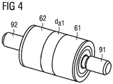
- FIG. 4 shows a perspective view of the surge arrester according to the in FIG. 2 Embodiment 2 shown.
- the surge arrester has a cylindrically arranged around the cavity 20 insulator 10.
- the insulator 10 is connected at its edges to the outer electrode 71 and the outer electrode 72.
- the connection electrodes 71, 72 are connected to connection bolts 91, 92.
- the outer metallization is arranged annularly on the outer surface S10b of the insulator.
- the two sections 61, 62 of the outer metallization are spaced apart by the distance d a1 .
Landscapes
- Chemical & Material Sciences (AREA)
- Engineering & Computer Science (AREA)
- Ceramic Engineering (AREA)
- Inorganic Chemistry (AREA)
- Power Engineering (AREA)
- Thermistors And Varistors (AREA)
- Emergency Protection Circuit Devices (AREA)
- Gas-Insulated Switchgears (AREA)
Description
- Die Erfindung betrifft einen Überspannungsableiter, bei dem die Ansprechstoßspannung reduziert ist.
- Überspannungsableiter lassen sich zum Schutz von Datenleitungen vor einer Überspannung, die mit der Datenleitung verbundene Kommunikationseinrichtung möglicherweise beschädigen würde, einsetzen. Ein weiteres Anwendungsgebiet, bei dem Überspannungsableiter zum Einsatz kommen, ist der Netzschutz. Ein Überspannungsableiter, der an eine Versorgungsleitung eines Wechselstromnetzes angeschlossen ist, dient beispielsweise dem Schutz der Versorgungsleitung vor einer Überspannung bei einem Blitzeinschlag.
- Im Unterschied zum Schutz von Datenleitungen, auf denen geringe Ströme fließen, treten auf Versorgungsleitungen in Wechselstromnetzen deutlich höhere Ströme von meistens über 100 A und gegenüber Datenleitungen auch deutlich erhöhte Spannungen, beispielsweise Spannungen von 110 V bis 400 V AC, auf. Beim Auftreten eines Spannungsimpulses auf der Versorgungsleitung in Folge eines Blitzschlages soll der Überspannungsableiter zünden, den Überspannungsimpuls nach Masse ableiten und anschließend wieder erlöschen.
- Derartige Ableiter für Versorgungsleitungen von Wechselstromnetzen müssen einen sogenannten Schutzpegel einhalten. In der Vorschrift DIN EN 61643-11 ist beispielsweise gefordert, dass die Ansprechspannung bei einem angelegten Spannungsimpuls der Form 1,2/50 µs mit einer Maximalamplitude von 6 kV einen Wert von typischerweise 1500 V nicht übersteigen darf, wobei gleichzeitig eine minimale Ansprechspannung von 500 V gefordert ist. Der Spannungsimpuls der Form 1,2/50 µs ist dabei ein Gleichspannungsimpuls, der innerhalb von 1,2 µs auf 6 kV ansteigt und innerhalb von 50 µs auf den halben Wert abklingt.
- In jüngster Zeit treten vermehrt Forderungen nach einer Reduzierung des Schutzpegels von beispielsweise den genannten 1500 V auf zum Beispiel 1000 V auf. Des Weiteren ist gefordert, dass trotz der Reduzierung des Schutzpegels andere charakteristische Parameter des Ableiters beibehalten werden sollen. Dies bedeutet de facto eine Reduzierung der Ansprechstoßspannung bei Beibehaltung der Ansprechgleichspannung des Ableiters. Beispielsweise soll bei einem Überspannungsableiter zwar die Ansprechstoßspannung reduziert werden, gleichzeitig aber beim Auftreten eines langsamen Spannungsanstieges auf der Leitung, beispielsweise eines Spannungsanstiegs von 400 V innerhalb von 5 ms, wie er im normalen Netzbetrieb vorkommen kann, kein Zünden des Ableiters vor Erreichen einer Ansprechgleichspannung von 600 V auftreten.
- Die
DE 10 2005 036 265 A1 offenbart einen Überspannungsableiter mit den Merkmalen des Oberbegriffs des Anspruchs 1. - Es besteht ein Bedarf daran, einen Überspannungsableiter anzugeben, bei dem die Ansprechstoßspannung unter Beibehaltung der Ansprechgleichspannung des Ableiters reduziert ist.
- Eine Ausführungsform eines derartigen Überspannungsableiters ist im Patentanspruch 1 angegeben.
- Der Überspannungsableiter umfasst einen elektrischen Isolator, der einen Hohlraum umgibt, eine Stiftelektrode und eine Rohrelektrode, die in dem Hohlraum angeordnet sind, wobei die Stiftelektrode in die Rohrelektrode hinein ragt. Auf einer dem Hohlraum zugewandten inneren Oberfläche des Isolators ist mindestens ein Zündstrich aufgetragen. Des Weiteren ist auf einer äußeren Oberfläche des Isolators eine Außenmetallisierung angeordnet.
- Durch das Aufbringen einer Außenmetallisierung auf dem Isolator, beispielsweise einem Isolator aus einem keramischen Material, in Verbindung mit einem koaxialen Aufbau der Elektroden kann die Ansprechstoßspannung unter Beibehaltung der Ansprechgleichspannung reduziert werden. Durch Kombination von äußeren metallischen Belägen mit einem koaxialen inneren Aufbau gelingt es, die Ansprechstoßspannung, beispielsweise auf einen Schutzpegel von 1000 V, zu reduzieren, wobei eine Ansprechgleichspannung von 600 V bei einem Spannungsanstieg von 400 V pro 5 ms erhalten bleibt. Feldsimulationen zeigen, dass durch diese Kombination beim Aufbau des Überspannungsableiters besonders hohe Feldstärken im Inneren des Ableiters erreicht werden können, insbesondere an der Spitze der Zündstriche, was zu Reduzierung der Ansprechstoßspannung führt.
- Die Außenmetallisierung kann beispielsweise ringförmig auf der äußeren Oberfläche des Isolators angebracht sein. Bei der ringförmigen Anordnung der Außenmetallisierung um den Umfang des Ableiters weist die Außenmetallisierung zwei Abschnitte auf. Die Abschnitte sind jeweils auf der äußeren Oberfläche des Isolators angeordnet und erstrecken sich jeweils von einem Rand der äußeren Oberfläche des Isolators ausgehend aufeinander zu. Die beiden Ränder der äußeren Oberfläche des Isolators sind dabei verschiedenen Anschlusselektroden des Überspannungsableiters zugewandt. Die äußere Oberfläche des Isolators kann an jedem ihrer Ränder mit einer der Anschlusselektroden des Überspannungsableiters verbunden sein. Einer der Abschnitte der äußeren Metallisierungsschicht kann mit der Stiftelektrode elektrisch verbunden sein und der andere der Abschnitte der äußeren Metallisierungsschicht kann mit der Rohrelektrode in elektrischem Kontakt stehen. Zwischen den Abschnitten der Außenmetallisierung, in etwa der Mitte der äußeren Oberfläche des Isolators, verbleibt ein Spalt, der frei vom Material der Außenmetallisierung ist und somit eine Isolationsstrecke darstellt.
- Bei einer anderen Ausführungsform kann sich die Außenmetallisierung auf der Oberfläche des Isolators einseitig von einem Rand der Oberfläche des Isolators, an dem der Isolator mit einer Anschlusselektrode des Überspannungsableiters verbunden ist, in Richtung auf den anderen Rand der äußeren Oberfläche des Isolators, der mit der anderen Anschlusselektrode verbunden ist, erstrecken. Die Außenmetallisierung erstreckt sich beispielsweise von demjenigen Rand der äußeren Oberfläche des Isolators, der der Stiftelektrode zugewandt ist, in Richtung auf den gegenüberliegenden Rand der äußeren Oberfläche des Isolators, der der Rohrelektrode zugewandt ist. Die Außenmetallisierung steht mit der Stiftelektrode in elektrischem Kontakt und endet in einem Abstand von dem Rand der äußeren Oberfläche des Isolators, der der Rohrelektrode zugewandt ist.
- Die Erfindung wird im Folgenden anhand von Figuren, die Ausführungsbeispiele der vorliegenden Erfindung zeigen, näher erläutert.
- Es zeigen:
- Figur 1
- eine Ausführungsform eines Überspannungsableiters ohne äußere Metallisierung mit einer Feldlinienverteilung vor einem Zünden des Ableiters,
- Figur 2
- eine Ausführungsform eines Überspannungsableiters mit einer zweiseitigen äußeren Metallisierung und einer zugehörigen Feldlinienverteilung vor einem Zünden des Ableiters,
- Figur 3
- eine Ausführungsform eines Überspannungsableiters mit einer einseitigen äußeren Metallisierung und einer zugehörigen Feldlinienverteilung vor einem Zünden des Ableiters,
- Figur 4
- eine perspektivische Ansicht einer Ausführungsform eines Überspannungsableiters mit zweiseitiger Außenmetallisierung.
-
Figur 1 zeigt eine Ausführungsform 1 eines elektrischen Bauelements eines Überspannungsableiters mit einem koaxialen Aufbau von Elektroden im Inneren des Spannungsableiters. Der Überspannungsableiter 1 umfasst einen elektrischen Isolator 10, der einen Hohlraum 20 umgibt. Der Isolator 10 kann ein keramisches Material, beispielsweise ein Material das Aluminiumoxid, enthalten. In dem Hohlraum 20 ist eine Stiftelektrode 30 und eine Rohrelektrode 40 angeordnet. Der Hohlraum 20 zwischen der Stiftelektrode 30, der Rohrelektrode 40 und dem elektrischen Isolator 10 kann mit einer Gasmischung, die beispielsweise einen Argon-Anteil von zirka 35 % bis 95 %, einen Wasserstoff-Anteil von 5 % bis 20 % und einen Neon-Anteil von bis zu 50 % enthält, gefüllt sein. - Die Stiftelektrode 30 ragt in die Rohrelektrode 40 hinein und ist elektrisch mit einer Anschlusselektrode 71 verbunden. Die Rohrelektrode 40 umgibt die Stiftelektrode 30 und ist elektrisch mit einer Anschlusselektrode 72 verbunden. Die Rohrelektrode und die Stiftelektrode sind derart angeordnet, dass zwischen ihnen ein Spalt 21 gebildet wird, der einen Entladungsraum des Überspannungsableiters bildet. Die Stiftelektrode und die Rohrelektrode können Kupfer, Eisen oder eine Wolfram-Kupfermischung enthalten. Die Anschlusselektroden 71, 72 können aus Kupfer oder Fe-Ni-Legierung hergestellt sein.
- Auf einer inneren Oberfläche S10a des Isolators 10, die dem Hohlraum 20 zugewandt ist, kann ein oder mehrere Zündstriche 50 aufgetragen sein. Der Zündstrich 50 kann ein Material aus Graphit enthalten. Durch einen derartigen Zündstrich kann vor allem ein gutes dynamisches Zündverhalten des Ableiterbauelements sichergestellt werden. Im Entladefall fließt ein Strom von der Anschlusselektrode 71 zur Stiftelektrode 30, über die Funkenstrecke des Entladungsraums 21 zur Rohrelektrode 40 und von dort zur Anschlusselektrode 72. Im Entladungsraum 21 erfolgt die Stoßstromentladung vor allem in radialer Weise.
- In
Figur 1 sind die bei der Stoßstromentladung auftretenden Feldlinien im rechten Teil des Überspannungsableiters eingezeichnet. Aus Vereinfachungsgründen ist der Feldlinienverlauf nur im rechten Teil des Überspannungsableiterbauelements eingezeichnet. Im linken Teil des Überspannungsableiters verlaufen die Feldlinien entsprechend. Die Feldlinien geben Äquipotenziallinien an. Die Feldlinien verlaufen durch den Entladungsraum 21 des Hohlraums 20 zwischen der Stiftelektrode 30 und Rohrelektrode 40 und im Teil des Hohlraums 20 zwischen dem Isolator 10 und die Rohrelektrode 40. Die Feldlinien treten an Restisolationsbereichen 11, 12 der inneren Oberfläche des Isolators, die nicht von dem Zündstrich 50 bedeckt sind, in die äußere Umgebung des Bauelements aus. - Bei den folgenden Ausführungsformen 2 und 3 des Überspannungsableiters sind gleiche Elemente wie in
Figur 1 mit gleichen Bezugszeichen bezeichnet. Es wird im Folgenden nur noch auf die Unterschiede zu der inFigur 1 gezeigten Ausführungsformen 1 des Überspannungsableiters eingegangen. Bei den Ausführungsformen 2 und 3 des Überspannungsableiters ist im Unterschied zur Ausführungsform 1 zusätzlich eine Außenmetallisierung auf einer äußeren Oberfläche S10b des Isolators 10 angeordnet. - Bei der in
Figur 2 gezeigten Ausführungsform 2 des Überspannungsableiters umfasst die Außenmetallisierung einen Abschnitt 61 und einen Abschnitt 62, die auf der äußeren Oberfläche S10b des Isolators in einem Abstand da1 angeordnet sind. Der Abschnitt 61 der Außenmetallisierung ist mit der Anschlusselektrode 71 verbunden und der Abschnitt 62 der Außenmetallisierung ist mit der Anschlusselektrode 72 verbunden. Der Abschnitt 61 der Außenmetallisierung erstreckt sich auf der äußeren Oberfläche S10b des Isolators 10 ausgehend von einem Rand R1 der äußeren Oberfläche des Isolators, der der Außenelektrode 71 bzw. der Stiftelektrode 30 zugewandt ist, in Richtung auf den Abschnitt 62 der Außenmetallisierung. Der Abschnitt 62 der Außenmetallisierung erstreckt sich auf der äußeren Oberfläche S10b des Isolators 10 ausgehend von einem dem Rand R1 gegenüberliegenden Rand R2 der äußeren Oberfläche des Isolators, der mit der Außenelektrode 72 verbunden ist bzw. der Rohrelektrode 40 zugewandt ist, in Richtung auf den Abschnitt 61 der Außenmetallisierung. Zwischen den Metallisierungsschichten 61 und 62 wird ein Spalt gebildet. - Die Spaltbreite bzw. der Abstand da1 zwischen dem Abschnitt 61 und dem Abschnitt 62 der Außenmetallisierung ist abhängig vom inneren Hauptelektrodenabstand di und dem Füllgasdruck pi der Gasentladungsstrecke 21. Wenn pa den Außendruck der Umgebung des Isolators (üblicherweise 1 at) und da1,min den minimalen Abstand der Metallisierung und 61, 62 im Spaltbereich bezeichnet, können die Abschnitte 61, 62 der Außenmetallisierung derart auf der äußeren Oberfläche S10b des Isolators angeordnet werden, dass sich der minimale Abstand zwischen den Metallisierungen zu da1,min = pi/pa * di ergibt.
- Um mögliche Gleitentladungseffekte einer Entladung auf der äußeren Oberfläche S10b des Isolatorkörpers 10 zu verhindern, kann der Außenabstand da1 mindestens so groß sein, wie das doppelte des Produkts aus dem Abstand di zwischen der Stiftelektrode 30 und der Rohrelektrode 40 und dem Quotienten aus dem Innendruck pi des Füllgases 80 im Hohlraum 20 und dem äußeren Atmosphärendruck pa der Umgebung des Überspannungsableiters. Vorausgesetzt werden dabei Füllgase mit einer ähnlichen Paschenkurve wie für Luft. Somit ergibt sich die Beziehung da1 > 2 * pi / pa * di bzw. für einen Außendruck von pa = 1 at ergibt sich da1 vorzugsweise zu da1 > 2 * pi * di.
- Sollte die Gasentladungsstrecke undicht werden, so sollte die Außenisolationsstrecke da1 größer sein als der Hauptelektrodenspalt di, da ansonsten anstelle einer Entladung im Entladungsraum 21 eine Außenentladung auftreten würde. Daher kann der Abstand da1 zu da1 > 2 * di gewählt werden.
- Der Zündstrich 50 kann in einem Abstand dz1 von der Außenelektrode 71 entfernt und in einem Abstand dz2 von der Außenelektrode 72 entfernt angeordnet sein. Die Länge des Abschnitts 61 der Außenmetallisierung kann größer als der Abstand dz1 des Zündstrichs sein. Die Länge des Abschnitts 62 der Außenmetallisierung kann größer als der Abstand dz2 des Zündstrichs sein.
-
Figur 3 zeigt eine Ausführungsform 3 des Überspannungsableiters, bei der als äußere Metallisierung nur eine Außenmetallisierungsschicht 63 auf der äußeren Oberfläche S10b des Isolators 10 angeordnet ist. Die Außenmetallisierung 63 erstreckt sich auf der äußeren Oberfläche S10b des Isolators ausgehend von dem Rand R1 der äußeren Oberfläche des Isolators, der der Anschlusselektrode 71 bzw. der Stiftelektrode 30 zugewandt ist, in Richtung auf den gegenüberliegenden Rand R2 der äußeren Oberfläche des Isolators, der der Anschlusselektrode 72 bzw. der Rohrelektrode 40 zugewandt ist. Die Außenmetallisierungsschicht 63 ist mit der Außenelektrode 71 verbunden und zu der Außenelektrode 72 im Abstand da2 angeordnet. Die Außenmetallisierung 63 endet in einem Abstand da2 von dem Rand R2 entfernt. - Der Zündstrich 50 ist in einem Abstand dz2 von der Außenelektrode 72 angeordnet. Der Abstand da2 der Außenmetallisierung 63 von der Außenelektrode 72, der der Restisolationsstrecke der Außenmetallisierung zur Gegenelektrode 72 entspricht, ist kürzer als der Abstand dz2 des Zündstrichs 50 von der Außenelektrode 72.
- Des Weiteren ist der Abstand da2 zwischen der Außenmetallisierung 63 und der Außenelektrode 72 mindestens so groß wie das Doppelte des Produkts aus dem Abstand di zwischen der Stiftelektrode 30 und der Rohrelektrode 40 und dem Quotienten aus dem Innendruck pi des im Hohlraum 20 befindlichen Füllgases 80 und dem äußeren Atmosphärendruck pa der Umgebung des Überspannungsableiters.
- Bei der Ausführungsform 3 des Überspannungsableiters ist der Abstand da2 der Außenmetallisierungsschicht 63 zur Außenelektrode 72 vom inneren Elektrodenabstand di, dem Füllgasdruck pi der Gasentladungsstrecke 21 sowie dem äußeren Atmosphärendruck pa abhängig. Der minimale Abstand da2,min der Außenmetallisierung 63 von der Anschlusselektrode 72 kann zu da2,min = pi/pa * di gewählt werden.
- Um mögliche Gleitentladungseffekte einer Entladung auf der äußeren Oberfläche S10b des Isolators 10 zu verhindern, sollte der Abstand da2 zwischen der Außenmetallisierung 63 und der Außenelektrode 72 das doppelte des Produkts aus dem Abstand di zwischen der Stiftelektrode 30 und der Rohrelektrode 40 und dem Quotienten aus dem Innendruck pi des Füllgases 80 im Hohlraum 20 und dem äußeren Atmosphärendruck pa der Umgebung des Überspannungsableiters betragen. Vorausgesetzt werden dabei Füllgase mit einer ähnlichen Paschenkurve wie für Luft. Somit ergibt sich die Beziehung da2 > 2 * pi / pa * di bzw. für einen Außendruck von pa = 1 at ergibt sich da2 vorzugsweise zu da2 > 2 * pi * di.
- Wenn die Gasentladungsstrecke undicht wird, so sollte die Außenisolationsstrecke da2 größer sein als der Hauptelektrodenspalt di, da ansonsten anstelle einer Entladung im Entladungsraum 21 eine Außenentladung auftreten würde. Daher kann der Abstand da2 zu da2 > 2 * di gewählt werden.
- In Abhängigkeit von den geforderten Spannungsanstiegen kann die Schichtdicke der Außenmetallisierungen 61, 62, 63 zwischen 3 µm bis 25 µm betragen. Es kann jedoch auch eine metallene Kappe mit einer Dicke im Millimeter-Bereich über den Isolator 10 geschoben werden.
- Wie den Feldlinienverteilungen in den
Figuren 2 und3 zu entnehmen ist, werden die Feldlinien an den Enden des Zündstrichs 50 und den Enden der Außenmetallisierung zusammengedrängt, so dass in diesen Bereichen hohe Feldstärken im Inneren des Ableiters erreicht werden, die zu einer Reduzierung der Ansprechstoßspannung der Bauelemente führen. Gleichzeitig kann durch die Ausführungsformen 2 und 3 des Überspannungsableiters die Ansprechgleichspannung, beispielsweise eine statische Zündspannung von zirka 600 V, beibehalten werden. -
Figur 4 zeigt eine perspektivische Ansicht des Überspannungsableiters gemäß der inFigur 2 gezeigten Ausführungsform 2. Der Überspannungsableiter weist einen um den Hohlraum 20 zylinderförmig angeordneten Isolator 10 auf. Der Isolator 10 ist an seinen Rändern mit der Außenelektrode 71 und der Außenelektrode 72 verbunden. Die Anschlusselektroden 71, 72 sind mit Anschlussbolzen 91, 92 verbunden. Die Außenmetallisierung ist ringförmig auf der äußeren Oberfläche S10b des Isolators angeordnet. Die beiden Abschnitte 61, 62 der Außenmetallisierung sind um den Abstand da1 beabstandet zueinander angeordnet. -
- 1, 2, 3
- Ausführungsformen des Überspannungsableiters
- 10
- Isolator
- 20
- Hohlraum
- 21
- Entladungsraum
- 30
- Stiftelektrode
- 40
- Rohrelektrode
- 50
- Zündstrich
- 61, 62, 63
- Außenmetallisierung
- 71, 72
- Anschlusselektroden
- 80
- Füllgas
- 91, 92
- Anschlussbolzen
Claims (12)
- Überspannungsableiter, umfassend:- einen elektrischen Isolator (10), der einen Hohlraum (20) umgibt,- eine Stiftelektrode (30) und eine Rohrelektrode (40), die in dem Hohlraum (20) angeordnet sind, wobei die Stiftelektrode (30) in die Rohrelektrode (40) hinein ragt,- wobei auf einer dem Hohlraum (20) zugewandten inneren Oberfläche (S10a) des Isolators mindestens ein Zündstrich (50) aufgetragen ist, dadurch gekennzeichnet, dass auf einer äußeren Oberfläche (S10b) des Isolators (10) eine Außenmetallisierung (61, 62, 63) angeordnet ist.
- Überspannungsableiter nach Anspruch 1,- wobei der Isolator (10) zylinderförmig um den Hohlraum (20) angeordnet ist,- wobei die Außenmetallisierung (61, 62, 63) ringförmig auf der äußeren Oberfläche (S10b) des Isolators (10) angeordnet ist.
- Überspannungsableiter nach einem der Ansprüche 1 oder 2, umfassend:- eine erste Anschlusselektrode (71), die mit der Stiftelektrode (30) zum Anlegen eines Spannungspotentials verbunden ist,- eine zweite Anschlusselektrode (72), die mit der Rohrelektrode (40) zum Anlegen eines Spannungspotentials verbunden ist.
- Überspannungsableiter nach einem der Ansprüche 1 bis 3, wobei die Außenmetallisierung einen ersten Abschnitt (61) und einen zweiten Abschnitt (62) umfasst, die auf der äußeren Oberfläche (S10b) des Isolators (10) in einem Abstand (da1) zueinander beabstandet angeordnet sind.
- Überspannungsableiter nach Anspruch 4,
wobei sich der erste Abschnitt (61) der Außenmetallisierung auf der äußeren Oberfläche (S10b) des Isolators (10) ausgehend von einem ersten Rand (R1) der äußeren Oberfläche des Isolators, der der ersten Außenelektrode (71) zugewandt ist, und der zweite Abschnitt (62) der Außenmetallisierung auf der äußeren Oberfläche (S10b) des Isolators (10) ausgehend von einem zweiten Rand (R2) der äußeren Oberfläche des Isolators, der zu dem ersten Rand (R1) gegenüberliegend angeordnet ist, aufeinander zu erstrecken. - Überspannungsableiter nach einem der Ansprüche 4 oder 5,- wobei der Zündstrich (50) in einem ersten Abstand (dz1) von der ersten Außenelektrode (71) angeordnet ist,- wobei die Länge des ersten Abschnitts (61) der Außenmetallisierung größer als der erste Abstand (dz1) des Zündstrichs (50) ist,- wobei der Zündstrich (50) in einem zweiten Abstand (dz2) von der zweiten Außenelektrode (72) angeordnet ist,- wobei die Länge des zweiten Abschnitts (62) der Außenmetallisierung größer als der zweite Abstand (dz2) des Zündstrichs (50) ist.
- Überspannungsableiter nach einem der Ansprüche 4 bis 6, wobei der Abstand (da1) zwischen dem ersten und zweiten Abschnitt (61, 62) der Außenmetallisierung mindestens so groß ist wie das Doppelte des Produkts aus dem Abstand (di) zwischen der Stiftelektrode (30) und der Rohrelektrode (40) und dem Quotienten aus dem Innendruck (pi) eines Füllgases im Hohlraum (20) und dem äußeren Atmosphärendruck (pa) der Umgebung des Überspannungsableiters.
- Überspannungsableiter nach einem der Ansprüche 4 bis 7,
wobei der erste Abschnitt (61) der Außenmetallisierung mit der ersten Anschlusselektrode (71) und der zweite Abschnitt (62) der Außenmetallisierung mit der zweiten Anschlusselektrode (72) verbunden ist. - Überspannungsableiter nach Anspruch 3,
wobei sich die Außenmetallisierung (63) ausgehend von einem ersten Rand (R1) der äußeren Oberfläche (S10b) des Isolators (10), der näher an der ersten Anschlusselektrode (71) als an der zweiten Anschlusselektrode (72) liegt, in Richtung auf einen zweiten Rand (R2) der äußeren Oberfläche (S10b) des Isolators, der dem ersten Rand (R1) gegenüber liegt, erstreckt und in einem Abstand (da2) von dem zweiten Rand (R2) angeordnet ist. - Überspannungsableiter nach Anspruch 3,
wobei die Außenmetallisierung (63) mit der ersten Außenelektrode (71) verbunden ist und zu der zweiten Außenelektrode (72) um den Abstand (da2) beabstandet angeordnet ist. - Überspannungsableiter nach einem der Ansprüche 9 oder 10,- wobei der Zündstrich (50) in einem Abstand (dz2) von der zweiten Außenelektrode (72) angeordnet ist,- wobei der Abstand (da2) der Außenmetallisierung (63) von der zweiten Außenelektrode (72) kürzer ist als der erste Abstand (dz1) des Zündstrichs (50).
- Überspannungsableiter nach einem der Ansprüche 9 bis 11, wobei der Abstand (da2) zwischen der Außenmetallisierung (63) und der zweiten Außenelektrode (72) mindestens so groß ist wie das Doppelte des Produkts aus dem Abstand (di) zwischen der Stiftelektrode (30) und der Rohrelektrode (40) und dem Quotienten aus dem Innendruck (pi) eines Füllgases (80) im Hohlraum (20) und dem äußeren Atmosphärendruck (pa) der Umgebung des Überspannungsableiters.
Applications Claiming Priority (2)
| Application Number | Priority Date | Filing Date | Title |
|---|---|---|---|
| DE102012103158A DE102012103158A1 (de) | 2012-04-12 | 2012-04-12 | Überspannungsableiter |
| PCT/EP2013/056429 WO2013152948A1 (de) | 2012-04-12 | 2013-03-26 | Überspannungsableiter |
Publications (2)
| Publication Number | Publication Date |
|---|---|
| EP2837073A1 EP2837073A1 (de) | 2015-02-18 |
| EP2837073B1 true EP2837073B1 (de) | 2018-06-27 |
Family
ID=47998443
Family Applications (1)
| Application Number | Title | Priority Date | Filing Date |
|---|---|---|---|
| EP13712547.2A Active EP2837073B1 (de) | 2012-04-12 | 2013-03-26 | Überspannungsableiter |
Country Status (5)
| Country | Link |
|---|---|
| US (1) | US9614370B2 (de) |
| EP (1) | EP2837073B1 (de) |
| JP (1) | JP6157587B2 (de) |
| DE (1) | DE102012103158A1 (de) |
| WO (1) | WO2013152948A1 (de) |
Families Citing this family (3)
| Publication number | Priority date | Publication date | Assignee | Title |
|---|---|---|---|---|
| CZ306224B6 (cs) * | 2012-08-22 | 2016-10-12 | Hakel Spol. S R. O. | Výkonová bleskojistka pro velké proudové zátěže, s prodlouženou životností |
| DE102013114546B4 (de) * | 2013-12-19 | 2017-05-11 | Epcos Ag | Computerimplementierbares Verfahren zur Simulation des elektrischen Verhaltens eines Ableiters |
| RU2719630C1 (ru) * | 2019-11-01 | 2020-04-21 | Владислав Борисович Наседкин | Коммутирующее устройство |
Family Cites Families (16)
| Publication number | Priority date | Publication date | Assignee | Title |
|---|---|---|---|---|
| DE6607772U (de) | 1968-01-24 | 1971-04-15 | Siemens Ag | Ueberspannungsableiter |
| DE7823295U1 (de) | 1978-08-03 | 1984-03-29 | Siemens AG, 1000 Berlin und 8000 München | Gasentladungsroehre, insbesondere ueberspannungsableiter |
| DE2834088A1 (de) * | 1978-08-03 | 1980-02-14 | Siemens Ag | Gasentladungsroehre, insbesondere ueberspannungsableiter |
| DE3042847A1 (de) | 1980-11-13 | 1982-06-09 | Siemens AG, 1000 Berlin und 8000 München | Gasentladungs-ueberspannungsableiter mit konzentrisch umschliessender fassung |
| DE3118137C2 (de) | 1981-05-07 | 1986-04-24 | Siemens AG, 1000 Berlin und 8000 München | Gasentladungs-Überspannungsableiter mit parallel geschalteter Luftfunkenstrecke |
| US4475055A (en) | 1982-01-28 | 1984-10-02 | The United States Of America As Represented By The United States Department Of Energy | Spark gap device for precise switching |
| JPS59108290A (ja) * | 1982-12-10 | 1984-06-22 | 日本電信電話株式会社 | 避雷管 |
| JPS607183U (ja) | 1983-06-25 | 1985-01-18 | 株式会社サンコ−シャ | 過電圧保護素子 |
| US4680665A (en) | 1985-12-03 | 1987-07-14 | Reliance Comm/Tec Corporation | Gas discharge arrester |
| EP0242688B1 (de) | 1986-04-22 | 1990-07-18 | Siemens Aktiengesellschaft | Überspannungsableiter |
| JPH0249387A (ja) * | 1988-08-10 | 1990-02-19 | Hakusan Seisakusho:Kk | 通信用ガス放電避雷器 |
| US5768082A (en) | 1995-09-29 | 1998-06-16 | Siemens Aktiengesellschaft | Gas-filled surge voltage protector |
| DE10253166A1 (de) | 2002-11-14 | 2004-05-27 | Epcos Ag | Kontaktelement und gasgefüllter Überspannungsableiter mit dem Kontaktelement |
| DE102005036265A1 (de) | 2005-08-02 | 2007-02-08 | Epcos Ag | Funkenstrecke |
| DE102007063316A1 (de) * | 2007-12-28 | 2009-07-02 | Epcos Ag | Überspannungsableiter mit niedriger Ansprechstoßspannung |
| DE102009006543A1 (de) | 2009-01-29 | 2010-08-05 | Epcos Ag | Überspannungsableiter |
-
2012
- 2012-04-12 DE DE102012103158A patent/DE102012103158A1/de not_active Ceased
-
2013
- 2013-03-26 US US14/391,694 patent/US9614370B2/en active Active
- 2013-03-26 EP EP13712547.2A patent/EP2837073B1/de active Active
- 2013-03-26 WO PCT/EP2013/056429 patent/WO2013152948A1/de not_active Ceased
- 2013-03-26 JP JP2015504896A patent/JP6157587B2/ja active Active
Non-Patent Citations (1)
| Title |
|---|
| None * |
Also Published As
| Publication number | Publication date |
|---|---|
| JP2015513202A (ja) | 2015-04-30 |
| EP2837073A1 (de) | 2015-02-18 |
| US20150077894A1 (en) | 2015-03-19 |
| DE102012103158A1 (de) | 2013-10-17 |
| US9614370B2 (en) | 2017-04-04 |
| WO2013152948A1 (de) | 2013-10-17 |
| JP6157587B2 (ja) | 2017-07-05 |
Similar Documents
| Publication | Publication Date | Title |
|---|---|---|
| EP1566868B1 (de) | Überspannungsschutzelement und Zündelement für ein Überspannungsschutzelement | |
| DE2346174B2 (de) | Ueberspannungsableiter | |
| DE102012022399A1 (de) | Zündkreis | |
| EP1258066B1 (de) | Druckfest gekapselte funkenstreckenanordnung zum ableiten von schädlichen störgrössen durch überspannungen | |
| EP0251010A1 (de) | Gasentladungsüberspannungsableiter | |
| DE102016006350A1 (de) | Zündkerze für eine Hochfrequenz-Zündanlage | |
| DE2832060A1 (de) | Schutzvorrichtung fuer insbesondere telefonleitungen gegen ueberspannung | |
| DE10018012B4 (de) | Druckfest gekapselte Funkenstreckenanordnung zum Ableiten von schädlichen Störgrößen durch Überspannungen | |
| EP1692751B1 (de) | Überspannungsschutzeinrichtung | |
| DE102012103158A1 (de) | Überspannungsableiter | |
| DE4141682A1 (de) | Ueberspannungsschutzelement | |
| DE102014015611B4 (de) | Überspannungsableiter | |
| EP3649709B1 (de) | Ableiter | |
| DE102007015364B4 (de) | Überspannungsschutzeinrichtung | |
| EP2392057B1 (de) | Überspannungsableiter | |
| EP3588706B1 (de) | Funkenstreckenanordnung mit zwei zündkreisen | |
| EP3039755B1 (de) | Überspannungsableiter | |
| DE102014015609B3 (de) | Überspannungsableiter | |
| DE10118210B4 (de) | Gekapselter Überspannungsableiter mit einer Funkenstreckenanordnung | |
| EP3127199B1 (de) | Überspannungsableiter | |
| DE102014015610B4 (de) | Überspannungsableiter | |
| EP1992051A1 (de) | Gekapselte, druckfest ausgeführte, nicht hermetisch dichte, grundkonstruktiv rotationssymmetrische hochleistungsfunkenstrecke | |
| DE102025123162A1 (de) | Gasfunkenstrecke | |
| EP2080253B1 (de) | Gekapselte, druckfest ausgeführte, nicht hermetisch dichte, rotationssymmetrische hochleistungsfunkenstrecke | |
| DE10120563A1 (de) | Überspannungsschutzelement und Überspannungsschutzeinrichtung |
Legal Events
| Date | Code | Title | Description |
|---|---|---|---|
| PUAI | Public reference made under article 153(3) epc to a published international application that has entered the european phase |
Free format text: ORIGINAL CODE: 0009012 |
|
| 17P | Request for examination filed |
Effective date: 20140930 |
|
| AK | Designated contracting states |
Kind code of ref document: A1 Designated state(s): AL AT BE BG CH CY CZ DE DK EE ES FI FR GB GR HR HU IE IS IT LI LT LU LV MC MK MT NL NO PL PT RO RS SE SI SK SM TR |
|
| AX | Request for extension of the european patent |
Extension state: BA ME |
|
| DAX | Request for extension of the european patent (deleted) | ||
| GRAP | Despatch of communication of intention to grant a patent |
Free format text: ORIGINAL CODE: EPIDOSNIGR1 |
|
| RIC1 | Information provided on ipc code assigned before grant |
Ipc: H01T 1/22 20060101ALI20171220BHEP Ipc: H01T 4/12 20060101ALI20171220BHEP Ipc: H01T 1/20 20060101AFI20171220BHEP |
|
| STAA | Information on the status of an ep patent application or granted ep patent |
Free format text: STATUS: GRANT OF PATENT IS INTENDED |
|
| INTG | Intention to grant announced |
Effective date: 20180125 |
|
| RAP1 | Party data changed (applicant data changed or rights of an application transferred) |
Owner name: EPCOS AG |
|
| GRAS | Grant fee paid |
Free format text: ORIGINAL CODE: EPIDOSNIGR3 |
|
| GRAA | (expected) grant |
Free format text: ORIGINAL CODE: 0009210 |
|
| STAA | Information on the status of an ep patent application or granted ep patent |
Free format text: STATUS: THE PATENT HAS BEEN GRANTED |
|
| AK | Designated contracting states |
Kind code of ref document: B1 Designated state(s): AL AT BE BG CH CY CZ DE DK EE ES FI FR GB GR HR HU IE IS IT LI LT LU LV MC MK MT NL NO PL PT RO RS SE SI SK SM TR |
|
| REG | Reference to a national code |
Ref country code: GB Ref legal event code: FG4D Free format text: NOT ENGLISH |
|
| REG | Reference to a national code |
Ref country code: AT Ref legal event code: REF Ref document number: 1013132 Country of ref document: AT Kind code of ref document: T Effective date: 20180715 |
|
| REG | Reference to a national code |
Ref country code: IE Ref legal event code: FG4D Free format text: LANGUAGE OF EP DOCUMENT: GERMAN |
|
| REG | Reference to a national code |
Ref country code: DE Ref legal event code: R096 Ref document number: 502013010482 Country of ref document: DE |
|
| PG25 | Lapsed in a contracting state [announced via postgrant information from national office to epo] |
Ref country code: LT Free format text: LAPSE BECAUSE OF FAILURE TO SUBMIT A TRANSLATION OF THE DESCRIPTION OR TO PAY THE FEE WITHIN THE PRESCRIBED TIME-LIMIT Effective date: 20180627 Ref country code: NO Free format text: LAPSE BECAUSE OF FAILURE TO SUBMIT A TRANSLATION OF THE DESCRIPTION OR TO PAY THE FEE WITHIN THE PRESCRIBED TIME-LIMIT Effective date: 20180927 Ref country code: SE Free format text: LAPSE BECAUSE OF FAILURE TO SUBMIT A TRANSLATION OF THE DESCRIPTION OR TO PAY THE FEE WITHIN THE PRESCRIBED TIME-LIMIT Effective date: 20180627 Ref country code: BG Free format text: LAPSE BECAUSE OF FAILURE TO SUBMIT A TRANSLATION OF THE DESCRIPTION OR TO PAY THE FEE WITHIN THE PRESCRIBED TIME-LIMIT Effective date: 20180927 Ref country code: FI Free format text: LAPSE BECAUSE OF FAILURE TO SUBMIT A TRANSLATION OF THE DESCRIPTION OR TO PAY THE FEE WITHIN THE PRESCRIBED TIME-LIMIT Effective date: 20180627 |
|
| REG | Reference to a national code |
Ref country code: NL Ref legal event code: MP Effective date: 20180627 |
|
| REG | Reference to a national code |
Ref country code: LT Ref legal event code: MG4D |
|
| REG | Reference to a national code |
Ref country code: DE Ref legal event code: R082 Ref document number: 502013010482 Country of ref document: DE Representative=s name: EPPING HERMANN FISCHER PATENTANWALTSGESELLSCHA, DE Ref country code: DE Ref legal event code: R081 Ref document number: 502013010482 Country of ref document: DE Owner name: TDK ELECTRONICS AG, DE Free format text: FORMER OWNER: EPCOS AG, 81671 MUENCHEN, DE |
|
| PG25 | Lapsed in a contracting state [announced via postgrant information from national office to epo] |
Ref country code: LV Free format text: LAPSE BECAUSE OF FAILURE TO SUBMIT A TRANSLATION OF THE DESCRIPTION OR TO PAY THE FEE WITHIN THE PRESCRIBED TIME-LIMIT Effective date: 20180627 Ref country code: RS Free format text: LAPSE BECAUSE OF FAILURE TO SUBMIT A TRANSLATION OF THE DESCRIPTION OR TO PAY THE FEE WITHIN THE PRESCRIBED TIME-LIMIT Effective date: 20180627 Ref country code: GR Free format text: LAPSE BECAUSE OF FAILURE TO SUBMIT A TRANSLATION OF THE DESCRIPTION OR TO PAY THE FEE WITHIN THE PRESCRIBED TIME-LIMIT Effective date: 20180928 Ref country code: HR Free format text: LAPSE BECAUSE OF FAILURE TO SUBMIT A TRANSLATION OF THE DESCRIPTION OR TO PAY THE FEE WITHIN THE PRESCRIBED TIME-LIMIT Effective date: 20180627 |
|
| PG25 | Lapsed in a contracting state [announced via postgrant information from national office to epo] |
Ref country code: NL Free format text: LAPSE BECAUSE OF FAILURE TO SUBMIT A TRANSLATION OF THE DESCRIPTION OR TO PAY THE FEE WITHIN THE PRESCRIBED TIME-LIMIT Effective date: 20180627 |
|
| PG25 | Lapsed in a contracting state [announced via postgrant information from national office to epo] |
Ref country code: PL Free format text: LAPSE BECAUSE OF FAILURE TO SUBMIT A TRANSLATION OF THE DESCRIPTION OR TO PAY THE FEE WITHIN THE PRESCRIBED TIME-LIMIT Effective date: 20180627 Ref country code: SK Free format text: LAPSE BECAUSE OF FAILURE TO SUBMIT A TRANSLATION OF THE DESCRIPTION OR TO PAY THE FEE WITHIN THE PRESCRIBED TIME-LIMIT Effective date: 20180627 Ref country code: RO Free format text: LAPSE BECAUSE OF FAILURE TO SUBMIT A TRANSLATION OF THE DESCRIPTION OR TO PAY THE FEE WITHIN THE PRESCRIBED TIME-LIMIT Effective date: 20180627 Ref country code: EE Free format text: LAPSE BECAUSE OF FAILURE TO SUBMIT A TRANSLATION OF THE DESCRIPTION OR TO PAY THE FEE WITHIN THE PRESCRIBED TIME-LIMIT Effective date: 20180627 Ref country code: CZ Free format text: LAPSE BECAUSE OF FAILURE TO SUBMIT A TRANSLATION OF THE DESCRIPTION OR TO PAY THE FEE WITHIN THE PRESCRIBED TIME-LIMIT Effective date: 20180627 Ref country code: IS Free format text: LAPSE BECAUSE OF FAILURE TO SUBMIT A TRANSLATION OF THE DESCRIPTION OR TO PAY THE FEE WITHIN THE PRESCRIBED TIME-LIMIT Effective date: 20181027 |
|
| PG25 | Lapsed in a contracting state [announced via postgrant information from national office to epo] |
Ref country code: ES Free format text: LAPSE BECAUSE OF FAILURE TO SUBMIT A TRANSLATION OF THE DESCRIPTION OR TO PAY THE FEE WITHIN THE PRESCRIBED TIME-LIMIT Effective date: 20180627 Ref country code: IT Free format text: LAPSE BECAUSE OF FAILURE TO SUBMIT A TRANSLATION OF THE DESCRIPTION OR TO PAY THE FEE WITHIN THE PRESCRIBED TIME-LIMIT Effective date: 20180627 Ref country code: SM Free format text: LAPSE BECAUSE OF FAILURE TO SUBMIT A TRANSLATION OF THE DESCRIPTION OR TO PAY THE FEE WITHIN THE PRESCRIBED TIME-LIMIT Effective date: 20180627 |
|
| REG | Reference to a national code |
Ref country code: DE Ref legal event code: R097 Ref document number: 502013010482 Country of ref document: DE |
|
| PLBE | No opposition filed within time limit |
Free format text: ORIGINAL CODE: 0009261 |
|
| STAA | Information on the status of an ep patent application or granted ep patent |
Free format text: STATUS: NO OPPOSITION FILED WITHIN TIME LIMIT |
|
| PG25 | Lapsed in a contracting state [announced via postgrant information from national office to epo] |
Ref country code: DK Free format text: LAPSE BECAUSE OF FAILURE TO SUBMIT A TRANSLATION OF THE DESCRIPTION OR TO PAY THE FEE WITHIN THE PRESCRIBED TIME-LIMIT Effective date: 20180627 |
|
| 26N | No opposition filed |
Effective date: 20190328 |
|
| PG25 | Lapsed in a contracting state [announced via postgrant information from national office to epo] |
Ref country code: SI Free format text: LAPSE BECAUSE OF FAILURE TO SUBMIT A TRANSLATION OF THE DESCRIPTION OR TO PAY THE FEE WITHIN THE PRESCRIBED TIME-LIMIT Effective date: 20180627 |
|
| PG25 | Lapsed in a contracting state [announced via postgrant information from national office to epo] |
Ref country code: MC Free format text: LAPSE BECAUSE OF FAILURE TO SUBMIT A TRANSLATION OF THE DESCRIPTION OR TO PAY THE FEE WITHIN THE PRESCRIBED TIME-LIMIT Effective date: 20180627 |
|
| REG | Reference to a national code |
Ref country code: CH Ref legal event code: PL |
|
| GBPC | Gb: european patent ceased through non-payment of renewal fee |
Effective date: 20190326 |
|
| PG25 | Lapsed in a contracting state [announced via postgrant information from national office to epo] |
Ref country code: LU Free format text: LAPSE BECAUSE OF NON-PAYMENT OF DUE FEES Effective date: 20190326 Ref country code: AL Free format text: LAPSE BECAUSE OF FAILURE TO SUBMIT A TRANSLATION OF THE DESCRIPTION OR TO PAY THE FEE WITHIN THE PRESCRIBED TIME-LIMIT Effective date: 20180627 |
|
| REG | Reference to a national code |
Ref country code: BE Ref legal event code: MM Effective date: 20190331 |
|
| PG25 | Lapsed in a contracting state [announced via postgrant information from national office to epo] |
Ref country code: IE Free format text: LAPSE BECAUSE OF NON-PAYMENT OF DUE FEES Effective date: 20190326 Ref country code: CH Free format text: LAPSE BECAUSE OF NON-PAYMENT OF DUE FEES Effective date: 20190331 Ref country code: GB Free format text: LAPSE BECAUSE OF NON-PAYMENT OF DUE FEES Effective date: 20190326 Ref country code: LI Free format text: LAPSE BECAUSE OF NON-PAYMENT OF DUE FEES Effective date: 20190331 |
|
| PG25 | Lapsed in a contracting state [announced via postgrant information from national office to epo] |
Ref country code: FR Free format text: LAPSE BECAUSE OF NON-PAYMENT OF DUE FEES Effective date: 20190331 Ref country code: BE Free format text: LAPSE BECAUSE OF NON-PAYMENT OF DUE FEES Effective date: 20190331 |
|
| PG25 | Lapsed in a contracting state [announced via postgrant information from national office to epo] |
Ref country code: TR Free format text: LAPSE BECAUSE OF FAILURE TO SUBMIT A TRANSLATION OF THE DESCRIPTION OR TO PAY THE FEE WITHIN THE PRESCRIBED TIME-LIMIT Effective date: 20180627 |
|
| PG25 | Lapsed in a contracting state [announced via postgrant information from national office to epo] |
Ref country code: PT Free format text: LAPSE BECAUSE OF FAILURE TO SUBMIT A TRANSLATION OF THE DESCRIPTION OR TO PAY THE FEE WITHIN THE PRESCRIBED TIME-LIMIT Effective date: 20181029 Ref country code: MT Free format text: LAPSE BECAUSE OF FAILURE TO SUBMIT A TRANSLATION OF THE DESCRIPTION OR TO PAY THE FEE WITHIN THE PRESCRIBED TIME-LIMIT Effective date: 20180627 |
|
| REG | Reference to a national code |
Ref country code: AT Ref legal event code: MM01 Ref document number: 1013132 Country of ref document: AT Kind code of ref document: T Effective date: 20190326 |
|
| PG25 | Lapsed in a contracting state [announced via postgrant information from national office to epo] |
Ref country code: AT Free format text: LAPSE BECAUSE OF NON-PAYMENT OF DUE FEES Effective date: 20190326 |
|
| PG25 | Lapsed in a contracting state [announced via postgrant information from national office to epo] |
Ref country code: CY Free format text: LAPSE BECAUSE OF FAILURE TO SUBMIT A TRANSLATION OF THE DESCRIPTION OR TO PAY THE FEE WITHIN THE PRESCRIBED TIME-LIMIT Effective date: 20180627 |
|
| PG25 | Lapsed in a contracting state [announced via postgrant information from national office to epo] |
Ref country code: HU Free format text: LAPSE BECAUSE OF FAILURE TO SUBMIT A TRANSLATION OF THE DESCRIPTION OR TO PAY THE FEE WITHIN THE PRESCRIBED TIME-LIMIT; INVALID AB INITIO Effective date: 20130326 |
|
| PG25 | Lapsed in a contracting state [announced via postgrant information from national office to epo] |
Ref country code: MK Free format text: LAPSE BECAUSE OF FAILURE TO SUBMIT A TRANSLATION OF THE DESCRIPTION OR TO PAY THE FEE WITHIN THE PRESCRIBED TIME-LIMIT Effective date: 20180627 |
|
| P01 | Opt-out of the competence of the unified patent court (upc) registered |
Effective date: 20230521 |
|
| PGFP | Annual fee paid to national office [announced via postgrant information from national office to epo] |
Ref country code: DE Payment date: 20260323 Year of fee payment: 14 |