EP2804231B1 - Organische Leuchtdiodenanzeige, elektronische Vorrichtung damit und Verfahren zur Herstellung der organischen Leuchtdiodenanzeige - Google Patents
Organische Leuchtdiodenanzeige, elektronische Vorrichtung damit und Verfahren zur Herstellung der organischen Leuchtdiodenanzeige Download PDFInfo
- Publication number
- EP2804231B1 EP2804231B1 EP14168329.2A EP14168329A EP2804231B1 EP 2804231 B1 EP2804231 B1 EP 2804231B1 EP 14168329 A EP14168329 A EP 14168329A EP 2804231 B1 EP2804231 B1 EP 2804231B1
- Authority
- EP
- European Patent Office
- Prior art keywords
- layer
- oled
- plastic
- flexible substrate
- plastic layer
- Prior art date
- Legal status (The legal status is an assumption and is not a legal conclusion. Google has not performed a legal analysis and makes no representation as to the accuracy of the status listed.)
- Active
Links
Images




Classifications
-
- H—ELECTRICITY
- H10—SEMICONDUCTOR DEVICES; ELECTRIC SOLID-STATE DEVICES NOT OTHERWISE PROVIDED FOR
- H10K—ORGANIC ELECTRIC SOLID-STATE DEVICES
- H10K77/00—Constructional details of devices covered by this subclass and not covered by groups H10K10/80, H10K30/80, H10K50/80 or H10K59/80
- H10K77/10—Substrates, e.g. flexible substrates
- H10K77/111—Flexible substrates
-
- H—ELECTRICITY
- H10—SEMICONDUCTOR DEVICES; ELECTRIC SOLID-STATE DEVICES NOT OTHERWISE PROVIDED FOR
- H10K—ORGANIC ELECTRIC SOLID-STATE DEVICES
- H10K50/00—Organic light-emitting devices
- H10K50/80—Constructional details
- H10K50/84—Passivation; Containers; Encapsulations
- H10K50/844—Encapsulations
-
- H—ELECTRICITY
- H10—SEMICONDUCTOR DEVICES; ELECTRIC SOLID-STATE DEVICES NOT OTHERWISE PROVIDED FOR
- H10K—ORGANIC ELECTRIC SOLID-STATE DEVICES
- H10K59/00—Integrated devices, or assemblies of multiple devices, comprising at least one organic light-emitting element covered by group H10K50/00
- H10K59/10—OLED displays
- H10K59/12—Active-matrix OLED [AMOLED] displays
- H10K59/1201—Manufacture or treatment
-
- H—ELECTRICITY
- H10—SEMICONDUCTOR DEVICES; ELECTRIC SOLID-STATE DEVICES NOT OTHERWISE PROVIDED FOR
- H10K—ORGANIC ELECTRIC SOLID-STATE DEVICES
- H10K59/00—Integrated devices, or assemblies of multiple devices, comprising at least one organic light-emitting element covered by group H10K50/00
- H10K59/10—OLED displays
- H10K59/12—Active-matrix OLED [AMOLED] displays
- H10K59/121—Active-matrix OLED [AMOLED] displays characterised by the geometry or disposition of pixel elements
- H10K59/1213—Active-matrix OLED [AMOLED] displays characterised by the geometry or disposition of pixel elements the pixel elements being TFTs
-
- H—ELECTRICITY
- H10—SEMICONDUCTOR DEVICES; ELECTRIC SOLID-STATE DEVICES NOT OTHERWISE PROVIDED FOR
- H10K—ORGANIC ELECTRIC SOLID-STATE DEVICES
- H10K59/00—Integrated devices, or assemblies of multiple devices, comprising at least one organic light-emitting element covered by group H10K50/00
- H10K59/10—OLED displays
- H10K59/12—Active-matrix OLED [AMOLED] displays
- H10K59/124—Insulating layers formed between TFT elements and OLED elements
-
- H—ELECTRICITY
- H10—SEMICONDUCTOR DEVICES; ELECTRIC SOLID-STATE DEVICES NOT OTHERWISE PROVIDED FOR
- H10K—ORGANIC ELECTRIC SOLID-STATE DEVICES
- H10K59/00—Integrated devices, or assemblies of multiple devices, comprising at least one organic light-emitting element covered by group H10K50/00
- H10K59/80—Constructional details
- H10K59/87—Passivation; Containers; Encapsulations
- H10K59/873—Encapsulations
-
- H—ELECTRICITY
- H10—SEMICONDUCTOR DEVICES; ELECTRIC SOLID-STATE DEVICES NOT OTHERWISE PROVIDED FOR
- H10K—ORGANIC ELECTRIC SOLID-STATE DEVICES
- H10K71/00—Manufacture or treatment specially adapted for the organic devices covered by this subclass
- H10K71/851—Division of substrate
-
- H—ELECTRICITY
- H10—SEMICONDUCTOR DEVICES; ELECTRIC SOLID-STATE DEVICES NOT OTHERWISE PROVIDED FOR
- H10K—ORGANIC ELECTRIC SOLID-STATE DEVICES
- H10K2102/00—Constructional details relating to the organic devices covered by this subclass
- H10K2102/301—Details of OLEDs
- H10K2102/311—Flexible OLED
-
- H—ELECTRICITY
- H10—SEMICONDUCTOR DEVICES; ELECTRIC SOLID-STATE DEVICES NOT OTHERWISE PROVIDED FOR
- H10K—ORGANIC ELECTRIC SOLID-STATE DEVICES
- H10K50/00—Organic light-emitting devices
- H10K50/80—Constructional details
- H10K50/84—Passivation; Containers; Encapsulations
- H10K50/841—Self-supporting sealing arrangements
-
- H—ELECTRICITY
- H10—SEMICONDUCTOR DEVICES; ELECTRIC SOLID-STATE DEVICES NOT OTHERWISE PROVIDED FOR
- H10K—ORGANIC ELECTRIC SOLID-STATE DEVICES
- H10K59/00—Integrated devices, or assemblies of multiple devices, comprising at least one organic light-emitting element covered by group H10K50/00
- H10K59/80—Constructional details
- H10K59/87—Passivation; Containers; Encapsulations
- H10K59/871—Self-supporting sealing arrangements
-
- H—ELECTRICITY
- H10—SEMICONDUCTOR DEVICES; ELECTRIC SOLID-STATE DEVICES NOT OTHERWISE PROVIDED FOR
- H10K—ORGANIC ELECTRIC SOLID-STATE DEVICES
- H10K71/00—Manufacture or treatment specially adapted for the organic devices covered by this subclass
-
- Y—GENERAL TAGGING OF NEW TECHNOLOGICAL DEVELOPMENTS; GENERAL TAGGING OF CROSS-SECTIONAL TECHNOLOGIES SPANNING OVER SEVERAL SECTIONS OF THE IPC; TECHNICAL SUBJECTS COVERED BY FORMER USPC CROSS-REFERENCE ART COLLECTIONS [XRACs] AND DIGESTS
- Y02—TECHNOLOGIES OR APPLICATIONS FOR MITIGATION OR ADAPTATION AGAINST CLIMATE CHANGE
- Y02E—REDUCTION OF GREENHOUSE GAS [GHG] EMISSIONS, RELATED TO ENERGY GENERATION, TRANSMISSION OR DISTRIBUTION
- Y02E10/00—Energy generation through renewable energy sources
- Y02E10/50—Photovoltaic [PV] energy
- Y02E10/549—Organic PV cells
-
- Y—GENERAL TAGGING OF NEW TECHNOLOGICAL DEVELOPMENTS; GENERAL TAGGING OF CROSS-SECTIONAL TECHNOLOGIES SPANNING OVER SEVERAL SECTIONS OF THE IPC; TECHNICAL SUBJECTS COVERED BY FORMER USPC CROSS-REFERENCE ART COLLECTIONS [XRACs] AND DIGESTS
- Y02—TECHNOLOGIES OR APPLICATIONS FOR MITIGATION OR ADAPTATION AGAINST CLIMATE CHANGE
- Y02P—CLIMATE CHANGE MITIGATION TECHNOLOGIES IN THE PRODUCTION OR PROCESSING OF GOODS
- Y02P70/00—Climate change mitigation technologies in the production process for final industrial or consumer products
- Y02P70/50—Manufacturing or production processes characterised by the final manufactured product
Definitions
- the present disclosure relates generally to organic light-emitting diode (OLED) displays. More specifically, the present disclosure relates to an OLED display including a flexible substrate, an electronic device including the OLED display, and a method of manufacturing said OLED display.
- OLED organic light-emitting diode
- An organic light-emitting diode (OLED) display is a self-emission type display that includes a hole injection electrode, an electron injection electrode, and an organic emission layer disposed therebetween. In such a display, light is emitted when holes injected from the hole injection electrode and electrons injected from the electron injection electrode are recombined in the organic emission layer.
- OLED displays have been attracting attention as a potential next generation display since the OLED display has desirable characteristics such as low power consumption, excellent luminance, and a high response speed.
- Embodiments of the present invention may provide an organic light-emitting diode (OLED) display including a flexible substrate that has a low water vapor transmission rate and high adhesive strength, as well as a method of manufacturing such an OLED display.
- OLED organic light-emitting diode
- US 2002/140347 A1 discloses a covered substrate comprising a flexible substrate layer and a plurality of cooperative barrier layers disposed on the substrate layer.
- US 6268695 B1 discloses an environmental barrier for an OLED, which has a foundation and a cover.
- US 2011/0193067 A1 discloses an organic light-emitting device including a barrier layer that includes a silicon oxide layer and a silicon-rich silicon nitride layer.
- EP 2091096 A1 discloses an encapsulated electronic device comprising a first barrier structure, second barrier structure, and an electronic device arranged between the first and the second barrier structure
- WO 2013/065812 A1 discloses an OLED disposed on a gas barrier layer, said gas barrier layer comprising inorganic barrier layers, resins and adhesive layers.
- an organic light-emitting diode (OLED) display including: a first plastic layer; a first barrier layer formed on the first plastic layer, the first barrier layer comprising an inorganic material; a first intermediate layer formed on the first barrier layer; a second plastic layer formed on the first intermediate layer; an OLED layer formed on the second plastic layer; and a thin-film encapsulation layer encapsulating the OLED layer, wherein the first intermediate layer comprises an amorphous material or a metal thin film, and wherein the first intermediate layer is configured to increase an adhesive strength between the first barrier layer and the second plastic layer.
- a method of manufacturing an organic light-emitting diode (OLED) display including: preparing a carrier substrate; forming a mother flexible substrate on the carrier substrate, wherein the mother flexible substrate comprises a first plastic layer, a first barrier layer comprising an inorganic material, a first intermediate layer, and a second plastic layer that are sequentially stacked on each other, wherein the first intermediate layer comprises an amorphous material or a metal thin film, and wherein the first intermediate layer is configured to increase an adhesive strength between the first barrier layer and the second plastic layer; forming a plurality of OLED layers on the mother flexible substrate; forming a thin-film encapsulation layer encapsulating the plurality of OLED layers; separating the carrier substrate and the mother flexible substrate; and dividing the mother flexible substrate into a plurality of display units each including one of the OLED layers.
- OLED organic light-emitting diode
- Thicknesses of various layers and regions in the drawings are expanded for clarity. Thicknesses of some layers and regions are exaggerated for convenience of explanation. It will be understood that when a layer, film, region, or plate is referred to as being "on" another layer, film, region, or plate, it may be directly on the other layer, film, region, or plate or intervening layers, films, regions, or plates elements may be present.
- the term "and/or" includes any and all combinations of one or more of the associated listed items. Expressions such as “at least one of,” when preceding a list of elements, modify the entire list of elements and do not modify the individual elements of the list.
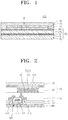
- FIG. 1 is a cross-sectional view of an organic light-emitting diode (OLED) display 100 according to an embodiment of the present invention.
- OLED organic light-emitting diode
- the OLED display 100 includes a flexible substrate FS, a thin-film transistor (TFT) layer 110, an OLED layer 120, and a thin-film encapsulation layer 130.
- TFT thin-film transistor
- the flexible substrate FS includes a first plastic layer 1PL, a first barrier layer 1BL, a first intermediate layer 1IL, a second plastic layer 2PL, and a second barrier layer 2BL.
- the first and second plastic layers 1PL and 2PL may be formed of a compliant plastic material having excellent thermal resistance and excellent durability, such as polyimide, polyethylene naphthalate, polyethylene terephthalate (PET), polyarylate, polycarbonate, polyether imide (PEI), or polyethersulfone.
- a compliant plastic material having excellent thermal resistance and excellent durability, such as polyimide, polyethylene naphthalate, polyethylene terephthalate (PET), polyarylate, polycarbonate, polyether imide (PEI), or polyethersulfone.
- an OLED layer 120 employing such plastic layers without any barrier layer is vulnerable to moisture or oxygen and is thus subject to deterioration. The lifespan of such an OLED display 100 may therefore be reduced.
- the first barrier layer 1BL is formed on the first plastic layer 1PL and the second barrier layer 2BL is formed on the second plastic layer 2PL.
- the first and second barrier layers 1BL and 2BL may be formed of an inorganic material, such as a metal oxide, a silicon nitride, or a silicon oxide, provided that the first barrier layer comprises an inorganic material.
- the first and second barrier layers 1BL and 2BL may each be made of a single layer or multilayer of an inorganic material, such as AlO 3 , SiO 2 , or SiN x .
- a water vapor transmission rate (WVTR) of the first and second barrier layers 1BL and 2BL formed of a single layer or multilayer may be lower than or equal to 10 -5 (g/m 2 /day).
- the first intermediate layer 1IL may be formed between the first barrier layer 1BL and the second plastic layer 2PL in order to increase an adhesive strength (peel strength) between the first barrier layer 1BL and the second plastic layer 2PL, as will be described in further detail later.
- the TFT layer 110 and the OLED layer 120 are formed on the flexible substrate FS.
- FIG. 2 is an enlarged view of a region II of FIG 1 , illustrating parts of the TFT layer 110 and the OLED layer 120 in further detail.
- a TFT including a semiconductor layer 111, a gate electrode 113, a source electrode 115, and a drain electrode 116 may be formed on the second barrier layer 2BL.
- a gate insulation film 112 may be formed between the semiconductor layer 111 and the gate electrode 113, and an interlayer insulation film 114 may be formed between the gate electrode 113 and the source electrode 115 and between the gate electrode 113 and the drain electrode 116.
- the semiconductor layer 111 may be made of amorphous silicon, an organic semiconductive material, or a conductive oxide.
- a top gate type TFT is shown, but embodiments of the present invention are not limited thereto. In other words, a TFT having any one of various structures, including a bottom gate type TFT, may be used.
- the TFT is directly formed on the second barrier layer 2BL, but embodiments of the present invention are not limited thereto.
- a buffer layer (not shown) may be further disposed between the second barrier layer 2BL and the TFT. Such a buffer layer flattens the flexible substrate FS and prevents impure elements from penetrating into the semiconductor layer 111 from the flexible substrate FS.
- silicon nitride and/or silicon oxide material may be arranged as a single layer or a plurality of layers (i.e. one or more layers of any one or more of these materials).
- at least one capacitor may be connected to the TFT.
- the TFT may be formed over the second plastic layer.
- the TFT may be formed on a suitable layer that is on the second plastic layer.
- a passivation layer 117 may be formed on the TFT, and a pixel-defining layer 122 may be formed on the passivation layer 117.
- the passivation layer 117 may protect the TFT and flatten a top surface of the TFT (i.e., provide an upper surface that is flatter than the TFT).
- An OLED may be connected to one of the source and drain electrodes 115 and 116 of the TFT.
- the OLED may include a pixel electrode 121, a counter electrode 124, and a layer 123 including at least an organic emission layer disposed between the pixel and counter electrodes 121 and 124.
- the layer 123 may be formed of a low molecular or high molecular organic material. When a low molecular organic material is used, the layer 123 may have a single or complex structure with a hole injection layer (HIL), a hole transport layer (HTL), an emission layer (EML), an electron transport layer (ETL), and an electron injection layer (EIL).
- HIL hole injection layer
- HTL hole transport layer
- EML emission layer
- ETL electron transport layer
- EIL electron injection layer
- the layer 123 may have a structure including an HTL and an EML.
- the layer 123 may form one unit pixel by using sub-pixels emitting red, green, and blue lights.
- the layer 123 may be formed as layers including emission materials emitting red, green, and blue lights that are perpendicularly stacked on each other, or with mixed emission materials. Of course, any other combination of colors may be used as long as a white light is emitted.
- the OLED display 100 may further include a color changing layer or color filter that changes the white light to a predetermined color.
- the counter electrode 124 may be variously modified, for example, may be formed to be continuous across a plurality of pixels.
- the pixel electrode 121 may operate as an anode and the counter electrode 124 may operate as a cathode, or vice versa. Also, at least one of the pixel electrode 121 and the counter electrode 124 may be a transparent electrode through which a light emitted from the EML penetrates.
- the OLED layer 120 is formed on the TFT layer 110 for convenience of description.
- parts of the TFT layer 110 and OLED layer 120 may be formed on the same layer.
- the gate electrode 113 of the TFT and the pixel electrode 121 of the OLED may be formed on the same layer.
- the thin-film encapsulation layer 130 encapsulating the OLED is formed on the flexible substrate FS.
- the thin-film encapsulation layer 130 may be formed of one or more inorganic layers or a combination that includes an inorganic layer and an organic layer.
- the organic layer may be formed of a polymer and, for example, may be a single layer or multiple stacked layers formed of any one of polyethylene terephthalate, polyimide, polycarbonate, epoxy, polyethylene, and polyacrylate.
- the organic layer may be formed of polyacrylate, and in more detail, may include a polymerized monomer composition including a diacrylate-based monomer and a triacrylate-based monomer. A monoacrylate-based monomer may be further included in the polymerized monomer composition.
- the polymerized monomer composition may further include a well known photoinitiator, such as TPO, but embodiments of the present invention are not limited thereto.
- the inorganic layer may be a single layer or multiple stacked layers, one or more of which includes a metal oxide or a metal nitride.
- the inorganic layer may include any one of SiN x , Al 2 O 3 , SiO 2 , and TiO 2 .
- An uppermost layer of the thin-film encapsulation layer 130 which is exposed at the exterior of the display 100, may be formed of an inorganic layer in order to prevent water vapor transmission to the OLED.
- the thin-film encapsulation layer 130 may include at least one sandwich structure wherein at least one organic layer is inserted between at least two inorganic layers.
- the thin-film encapsulation layer 130 may include at least one sandwich structure wherein at least one inorganic layer is inserted between at least two organic layers.
- the thin-film encapsulation layer 130 may include a first inorganic layer, a first organic layer, and a second inorganic layer sequentially stacked from a top of the OLED.
- the thin-film encapsulation layer 130 may include a first inorganic layer, a first organic layer, a second inorganic layer, a second organic layer, and a third inorganic layer sequentially stacked from the top of the OLED.
- the thin-film encapsulation layer 130 may include a first inorganic layer, a first organic layer, a second inorganic layer, a second organic layer, a third inorganic layer, a third organic layer, and a fourth inorganic layer sequentially stacked from the top of the OLED.
- a halogenated metal layer including LiF may be further disposed between the OLED and the first inorganic layer.
- the halogenated metal layer may prevent the OLED from being damaged while forming the first inorganic layer, and may be formed via a sputtering method or a plasma deposition method.
- the first organic layer may have a smaller area than the second inorganic layer, and the second organic layer may have a smaller area than the third inorganic layer. Also, the first organic layer may be completely covered by the second inorganic layer, and the second organic layer may be completely covered by the third inorganic layer.
- the thin-film encapsulation layer 130 is directly formed on the counter electrode 124, but alternatively, another component, such as a filler or an adhesive material, may be further disposed between the counter electrode 124 and the thin-film encapsulation layer 130.
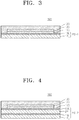
- FIG. 3 is a cross-sectional view of an OLED display 101 according to a comparative example.
- the OLED display 101 includes a flexible substrate FS-1, the TFT layer 110, the OLED layer 120, and the thin-film encapsulation layer 130.
- the flexible substrate FS-1 includes the first plastic layer 1PL and the first barrier layer 1BL. In other words, the flexible substrate FS-1 includes one plastic layer and one barrier layer.
- the first barrier layer 1BL may be damaged, for example, cracked, due to impurities or retraction defects formed on the first plastic layer 1PL and/or the first barrier layer 1BL. Moisture or oxygen may penetrate through such a damaged surface, and thus the OLED may be damaged.
- FIG. 4 is a cross-sectional view of an OLED display 102 according to another embodiment of the present invention.
- the OLED display 102 includes a flexible substrate FS-2, the TFT layer 110, the OLED layer 120, and the thin-film encapsulation layer 130.
- the flexible substrate FS-2 includes the first plastic layer 1PL, the first barrier layer 1BL, the second plastic layer 2PL, and the second barrier layer 2BL.
- a structure that includes a plastic layer and a barrier layer formed on the plastic layer is formed twice.
- a first intermediate layer 1IL (not shown in FIG. 4 ) is formed on the first barrier layer, with the second plastic layer 2PL formed on the first intermediate layer.
- Impurities or retraction defects may be randomly formed not only in the first plastic layer 1PL and the first barrier layer 1BL, but also in the second plastic layer 2PL and the second barrier layer 2BL.
- the OLED since an average water vapor transmission path from a defected region to an OLED is longer in the OLED display 102 than the OLED display 101, the OLED may be prevented from being damaged even if the first barrier layer 1BL and/or the second barrier layer 2BL are damaged, for example, cracked.
- dark spot defects may be reduced as the flexible substrate FS-2 has a lower water vapor transmission, but since an adhesive strength between the first barrier layer 1BL that is an inorganic film and the second plastic layer 2PL that is an organic film is relatively weak, the first barrier layer 1BL and the second plastic layer 2PL may be detached from each other during manufacture.
- the first barrier layer 1BL and the second plastic layer 2PL are not detached from each other since the first intermediate layer 1IL improving the adhesive strength between the first barrier layer 1BL and the second plastic layer 2PL is formed between the first barrier layer 1BL and the second plastic layer 2PL.
- the first intermediate layer 1IL may include an amorphous material.
- the first intermediate layer 1IL may include amorphous silicon as an example of the amorphous material.
- the first intermediate layer 1IL may include a metal thin film.
- the metal thin film may include at least one selected from among aluminum (A1), titanium (Ti), and molybdenum (Mo).
- A1 aluminum
- Ti titanium
- Mo molybdenum
- a material of the first intermediate layer 1IL is not limited to any of these in embodiments of the present invention, and any material is contemplated so long as the adhesive strength between the first barrier layer 1BL and the second plastic layer 2PL is improved.
- the first intermediate layer 1IL may have a UV light transmittance of at least 10% so that the second plastic layer 2PL is smoothly separated from a glass substrate GS during a process of separating a mother flexible substrate MFS and the glass substrate GS, which is described later with reference to FIGS. 11A and 11B . Accordingly, the first intermediate layer 1IL may have a thickness that is less than or equal to about 10 nm (100 ⁇ ).
- Table 1 below shows detachment evaluation results between the first barrier layer 1BL and the second plastic layer 2PL before a structure that does not include a first intermediate layer 1IL in the flexible substrate FS-2 is divided into display units.
- Sample 1 uses a SiO 2 single layer
- Sample 2 uses a SiN x single layer
- Sample 3 uses a SiO 2 /SiN x /SiO 2 complex layer
- Sample 4 uses a SiN x /SiO 2 /SiN x complex layer, as the first and second barrier layers 1BL and 2BL gf/inch equals 0.386089 N/m.
- Table 2 below shows detachment evaluation results between the first barrier layer 1BL and the second plastic layer 2PL in a unit of a display, after a structure that does not include the first intermediate layer 1IL in the flexible substrate FS-2 is divided into display units.
- Sample 5 uses a SiN x /SiO 2 complex layer and Sample 6 uses a SiN x /SiO 2 /SiN x complex layer as the first and second barrier layers 1BL and 2BL.
- Table 3 below shows detachment evaluation results between the first barrier layer 1BL and the second plastic layer 2PL before a structure that includes a first intermediate layer 1IL in the flexible substrate FS is divided into display units.
- Sample 7 uses ITO
- Sample 8 uses Ti
- Sample 9 uses Al, as the first intermediate layer 1IL.
- Sample 10 uses a-Si as the first intermediate layer 1IL and the a-Si is deposited for a duration of 5 seconds.
- Sample 11 uses a-Si as the first intermediate layer 1IL and the a-Si is deposited for a duration of 10 seconds.
- the first and second barrier layers 1BL and 2BL are formed by using a SiN x /SiO 2 complex layer respectively in thicknesses of 60 nm (600 ⁇ ) and 150 nm (1500 ⁇ ).
- Sample 8 (Ti)
- Sample 9 (Al)
- Sample 10 (a-Si)
- Sample 11 (a-Si) Average Adhesive Strength (gf/inch) Undetachable Undetachable Undetachable Undetachable 126.27 328.24
- Table 4 below shows detachment evaluation results between the first barrier layer 1BL and the second plastic layer 2PL in a display unit after the structure that includes the first intermediate layer 1IL on the flexible substrate FS is divided into display units.
- Samples 7 through 11 are the same as those in Table 3.
- Table 4 Intermediate Layer Sample 7 (ITO) Sample 8 (Ti)
- Sample 9 Sample 9
- Sample 10 (a-Si)
- Sample 11 (a-Si) Average Adhesive Strength (gf/inch) Undetachable Undetachable Undetachable Undetachable Undetachable Undetachable Undetachable Undetachable Undetachable
- an average adhesive strength between the first barrier layer 1BL and the second plastic layer 2PL is from about 60 to about 200 gf/inch, and referring to Table 2, an average adhesive strength between the first barrier layer 1BL and the second plastic layer 2PL in a display unit after the structure is divided into display units is from about 35 to about 40 gf/inch, i.e., low.
- an average adhesive strength between the first barrier layer 1BL and the second plastic layer 2PL for an a-Si first intermediate layer 1IL is from about 100 to about 300 gf/inch
- the first barrier layer 1BL and the second plastic layer 2PL are undetachable in the metal thin film.
- the first barrier layer 1BL and the second plastic layer 2PL are undetachable in a display unit after the structure that includes the first intermediate layer 1IL is divided into display units, and thus an average adhesive strength is not measurable.
- an adhesive strength between the first barrier layer 1BL and the second plastic layer 2PL significantly increases.
- an adhesive strength between a lower barrier layer and an adjacent upper plastic layer is increased so as to improve detachment defects of a display, by alternately stacking two plastic layers and two barrier layers and disposing an intermediate layer between the adjacent plastic and barrier layers to form the flexible substrate FS.
- FIGS. 5A through 10 are views for describing a method of manufacturing the OLED display 100, according to an embodiment of the present invention.
- FIG. 5A is a plan view for describing a process of forming the mother flexible substrate MFS on the glass substrate GS
- FIG. 5B is a cross-sectional view taken along a line VB-VB of FIG. 5A .
- the mother flexible substrate MFS is formed on the glass substrate GS.
- the mother flexible substrate MFS is formed of a plastic material and bends or is stretched when heat is applied, and thus it is difficult to precisely form thin film patterns, such as various electrodes or conductive wires, on the mother flexible substrate MFS. Accordingly, several thin film patterns are formed while adhering the mother flexible substrate MFS to the glass substrate GS that is a carrier substrate.
- a first plastic layer 1PS is formed on the glass substrate GS.
- the first plastic layer 1PL may be formed by coating and hardening a plastic polymer solution including at least one of polyimide, polyethylene naphthalate, polyethylene terephthalate, polyarylate, polycarbonate, polyether imide, and polyethersulfone on the glass substrate GS, or by laminating a polymer film on the glass substrate GS.
- a hardening method include a heat hardening method, a UV hardening method, and an electronic beam hardening method.
- the first barrier layer 1BL is formed on the first plastic layer 1PS.
- the first barrier layer 1BL may be formed in a single layer or a multilayer configuration containing an inorganic material, such as AlO 3 , SiO 2 , or SiN x , via chemical vapor deposition (CVD), plasma enhanced chemical vapor deposition (PECVD), or atomic layer deposition (ALD).
- CVD chemical vapor deposition
- PECVD plasma enhanced chemical vapor deposition
- ALD atomic layer deposition
- the first intermediate layer 1IL is formed on the first barrier layer 1BL.
- the first intermediate layer 1IL may be formed in a single layer or a multilayer configuration containing an amorphous material, such as amorphous silicon, or a metal thin film, such as ITO, Al, Ti, or Mo, via CVD, PECVD, or ALD.
- the second plastic layer 2PL is formed on the first intermediate layer 1IL.
- the second plastic layer 2PL may be formed of the same material as the first plastic layer 1PL via the same method.
- the second plastic layer 2PL may have lower viscosity than the first plastic layer 1PL.
- a high viscosity coating solution includes many impurities, and these impurities may also be coated.
- the second plastic layer 2PL may have lower viscosity than the first plastic layer 1PL so that filtering can be performed while coating the second plastic layer 2PL.
- impurities may be reduced by forming the second plastic layer 2PL using a filtered material, and since a coating material forming the second plastic layer 2PL has low viscosity, impurities present in the first plastic layer 1PL and the first barrier layer 1BL may be covered.
- first plastic layer 1PL and the second plastic layer 2PL have the same thickness in FIGS. 1 and 5A , but embodiments of the present invention are not limited thereto.
- Penetration times of oxygen and moisture penetrating from outside the flexible substrate FS are affected more by the thickness of the second plastic layer 2PL, which is closer to the OLED layer 120, than by that of the first plastic layer 1PL. Accordingly, by forming the second plastic layer 2PS closer to the OLED layer 120 to be thicker than the first plastic layer 1PL, penetration times are increased, thereby more effectively preventing deterioration of an OLED.
- the second barrier layer 2BL is formed on the second plastic layer 2PL.
- the second barrier layer 2BL may be formed of the same material as the first barrier layer 1BL via the same method.
- FIG. 6A is a plan view for describing a process of forming a plurality of units of OLED displays 100 on the mother flexible substrate MFS
- FIG. 6B is a cross-sectional view taken along a line VIB-VIB of FIG. 6A .
- the plurality of units of OLED displays 100 are formed on the mother flexible substrate MFS.
- the semiconductor layer 111 may be formed via a deposition method, such as a PECVD method, an atmosphere pressure CVD (APCVD) method, or a low pressure CVD (LPCVD) method, and when an organic TFT is applied as the semiconductor layer 111, a coating method or a printing method may be used.
- a deposition method such as a PECVD method, an atmosphere pressure CVD (APCVD) method, or a low pressure CVD (LPCVD) method
- APCVD atmosphere pressure CVD
- LPCVD low pressure CVD
- amorphous silicon may be crystallized by using any one of various crystallization methods, such as rapid thermal annealing (RTA), solid phase crystallization (SPC), excimer laser annealing (ELA), metal induced crystallization (MIC), metal induced lateral crystallization (MILC), and sequential lateral solidification (SLS).
- RTA rapid thermal annealing
- SPC solid phase crystallization
- ELA excimer laser annealing
- MIC metal induced crystallization
- MILC metal induced lateral crystallization
- SLS sequential lateral solidification
- the gate electrode 113 (refer to FIG. 2 ), the source electrode 115 (refer to FIG. 2 ), the drain electrode 116 (refer to FIG. 2 ), a capacitor (not shown), and various wires (not shown) may be deposited on the TFT layer 110 via CVD, PECVD, or ALD, and the TFT layer 110 may be patterned via a photolithography process.
- the layer 123 (refer to FIG. 2 ) including the organic emission layer of the OLED layer 120 may be formed via any one of various methods, such as a deposition method, a coating method, a printing method, and a light-heat transfer method.
- a buffer layer may be further disposed between the second barrier layer 2BL and the TFT layer 110.
- FIG. 7 is a cross-sectional view for describing a process of forming the thin-film encapsulation layer 130 for encapsulating a plurality of the OLED layers 120 on the mother flexible substrate MFS.
- the thin-film encapsulation layer 130 may be formed as a plurality of inorganic layers or a combination of one or more inorganic layers and one or more organic layers.
- the inorganic layer and the organic layer may be formed via any one of various methods, such as a CVD method, a PECVD method, and a sputtering method.
- the thin-film encapsulation layer 130 commonly covers the entire plurality of units of OLED displays 100, but embodiments of the present invention are not limited thereto. In other words, the thin-film encapsulation layer 130 may individually cover the units of OLED displays 100.
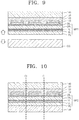
- FIGS. 8 and 9 are cross-sectional views for describing a process of separating the glass substrate GS and the mother flexible substrate MFS.
- a laser beam is irradiated onto a surface of the glass substrate GS opposite to where the mother flexible substrate MFS is formed.
- the laser beam may be a UV light irradiated by using an excimer laser.
- the irradiated UV light penetrates through the glass substrate GS, and is absorbed by the first and second plastic layers 1PL and 2PL.
- a binding force between the first and second plastic layers 1PL and 2PL and the glass substrate GS is weakened by the absorbed energy.
- the first and second barrier layers 1BL and 2BL are easily broken by externally-applied tension. Accordingly, by suitably applying the external tension to the mother flexible substrate MFS and the glass substrate GS in directions indicated by arrows of FIG. 9 (i.e. pulling the substrate MFS away from the glass substrate GS in a direction perpendicular to the surface of the glass substrate GS on which the substrate MFS is attached), the mother flexible substrate MFS may be separated from the glass substrate GS.
- a first protection film 140 may be adhered to the thin-film encapsulation layer 130 before the process of separating the mother flexible substrate MFS and the glass substrate GS.
- the first protection film 140 may be an optical member, such as a polarization film.
- FIG. 10 is a cross-sectional view for describing a process of dividing the OLED layer 120 formed on the mother flexible substrate MFS into the plurality of units of OLED displays 100.
- a second protection film 150 is adhered to a rear surface of the mother flexible substrate MFS, and then the mother flexible substrate MFS may be divided into the plurality of units of OLED displays 100.
- the second protection film 150 may be an optical member, such as a polarization film.
- the OLED layer 120 formed on the mother flexible substrate MFS may be divided into the plurality of units of OLED displays 100 by cutting the mother flexible substrate MFS along a cutting line CL in a non-display region between the OLED displays 100, using a cutting wheel or a laser cutter.
- a method of manufacturing a mother flexible substrate MFS-1 of the OLED display 100 according to another embodiment of the present invention will now be described with reference to FIGS. 11A and 11B .
- FIG. 11A is a plan view for describing a process of forming the mother flexible substrate MFS-1 on the glass substrate GS
- FIG. 11B is a cross-sectional view taken along a line XIB-XIB of FIG. 11A.
- FIGS. 11A and 11B particularly illustrate in detail an outer region of bonding surfaces of the glass substrate GS and the mother flexible substrate MFS-1.
- the first plastic layer 1PL and the second plastic layer 2PL formed on the glass substrate GS are respectively covered by the first barrier layer 1BL and the second barrier layer 2BL.
- the organic coating solution flows outside the glass substrate GS while forming the first and second plastic layers 1PL and 2PL on the glass substrate GS via a coating process, the organic coating solution that flowed outside the glass substrate GS generates a defect. Accordingly, the first and second plastic layers 1PL and 2PL are coated in a region smaller than the glass substrate GS.
- the first and second barrier layers 1BL and 2BL are formed via a deposition method, such as CVD or PECVD, the first and second barrier layers 1BL and 2BL are formed closer to an end of the glass substrate GS than the first and second plastic layers 1PL and 2PL.
- the second plastic layer 2PL extends beyond the outer edges of, the first plastic layer 1PL. Even if the second plastic layer 2PL is formed at the same location as the first plastic layer 1PL, in this embodiment, the second plastic layer 2PL flows over and beyond an outer region of the first plastic layer 1PL due to fluidity of the coating solution.
- the first intermediate layer 1IL has the same size (in plan view) as the first and second barrier layers 1BL and 2BL. Accordingly, the outer region of the mother flexible substrate MFS-1 has an overlapping region OA where a first intermediate layer 1IL-1 and the second plastic layer 2PL overlap each other.
- the first intermediate layer 1IL-1 may be formed such that the UV light suitably penetrates therethrough.
- the first intermediate layer 1IL-1 may have UV light transmittance of at least 10%.
- the first intermediate layer 1IL-1 may have the UV light transmittance of at least 10% by suitably adjusting a thickness of the first intermediate layer 1IL-1 by adjusting a time of forming the first intermediate layer 1IL-1.
- the thickness of the first intermediate layer 1IL-1 may be less than or equal to about 10 nm (100 ⁇ ).
- FIG. 12 is a cross-sectional view for describing a method of manufacturing the OLED display 100 of FIG. 1 , according to an embodiment of the present invention.
- a first intermediate layer 1IL-2 is formed to be smaller than or equal in area to the first plastic layer 1PL while forming a mother flexible substrate MFS-2.
- the UV light transmittance of the first intermediate layer 1IL-1 is adjusted by adjusting the thickness of the first intermediate layer 1IL-1 in the overlapping region OA of the outer region of the mother flexible substrate MFS-1, whereas in FIG. 12 , the first intermediate layer 1IL-2 is formed to be smaller than or equal in area to the first plastic layer 1PL so that no overlapping region OA is formed.
- an end of the second plastic layer 2PL and an end of the first barrier layer 1BL directly contact each other at an end of the glass substrate GS. Accordingly, the mother flexible substrate MFS-2 may be smoothly separated from the glass substrate GS.
- FIG. 13 is a cross-sectional view for describing a method of manufacturing the OLED display 100 of FIG. 1 , according to another embodiment of the present invention.
- a second plastic layer 2PL-3 is formed to be smaller than or equal in area to the first plastic layer 1PL while forming a mother flexible substrate MFS-3.
- the overlapping region OA of the second layer 2PL-3 and the first intermediate layer 1IL is not formed in the outer region as described above with reference to FIG. 12 . Accordingly, the mother flexible substrate MFS-3 and the glass substrate GS may be more easily separated from each other.
- an area of the second plastic layer 2PL-3 may be designed smaller than the actual area that is formed during a designing process.
- FIG. 14 is a cross-sectional view of an OLED display 200 according to another embodiment of the present invention.
- the OLED display 200 includes the flexible substrate FS-2, the TFT layer 110, the OLED layer 120, and the thin-film encapsulation layer 130.
- the current embodiment will be described mainly based on differences between the OLED display 200 and the OLED display 100, and like reference numerals shall be understood based on the above descriptions thereof.
- the flexible substrate FS-2 of the OLED display 200 includes the first plastic layer 1PL, the first barrier layer 1BL, a first intermediate layer 1IL-4, the second plastic layer 2PL and the second barrier layer 2BL.
- the first intermediate layer 1IL-4 of the current embodiment is patterned to be located in a region where the OLED layer 120 is formed. That is, the first intermediate layer 1IL-4 overlaps the TFT layer 110 and OLED layer 120.
- layer 1IL-4 is of approximately the same size, i.e. surface area, as layers 110 and 120, although embodiments of the invention contemplate layers 1IL-4 that are of differently sized area than layers 110 and 120.
- FIGS. 15A and 15B are respectively a plan view and a cross-sectional view for describing a method of manufacturing the OLED display 200 of FIG. 14 , according to an embodiment of the present invention.
- FIG. 15A is a plan view for describing a process of forming a mother flexible substrate MFS-4 on the glass substrate GS
- FIG. 15B is a cross-sectional view taken along line XVB-XVB of FIG. 15A .
- the first plastic layer 1PL and the first barrier layer 1BL are sequentially formed on the glass substrate GS, and then the first intermediate layer 1IL-4 is formed.
- the first intermediate layer 1IL-4 is formed only in regions corresponding to units of OLED displays 200, and is not formed in a non-display region between the OLED displays 200. That is, the intermediate layers 1IL-4 are only formed under the OLED displays 200, i.e. the intermediate layers 1IL-4 are of substantially the same size and shape (and thus have the same surface area) as the OLED displays 200, and are positioned so that each layer 1IL-4 substantially completely overlaps with its corresponding OLED display 200. Accordingly, in dividing the mother flexible substrate MFS-4 into the plurality of units of OLED displays 200, an inorganic layer, such as the first intermediate layer 1IL-4, is formed without reaching a cutting line so that a crack or contamination generated in the inorganic layer by cutting is reduced.
- the first intermediate layer 1IL-4 is not formed at (i.e. does not extend to) the end of the glass substrate GS, the first intermediate layer 1IL-4 and the second plastic layer 2PL do not overlap at the end of the glass substrate GS.
- the end of the second plastic layer 2PL and the end of the first barrier layer 1BL directly contact each other at or near the end of the glass substrate GS. Accordingly, the mother flexible substrate MFS-4 and the glass substrate GS may be more easily separated from each other.
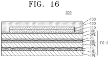
- FIG. 16 is a cross-sectional view of an OLED display 300 according to another embodiment of the present invention.
- the OLED display 300 includes a flexible substrate FS-3, the TFT layer 110, the OLED layer 120, and the thin-film encapsulation layer 130.
- the current embodiment will be described mainly based on differences between the OLED display 300 and the OLED display 100, and like reference numerals shall be understood based on the above descriptions thereof.
- the flexible substrate FS-3 of the OLED display 300 includes the first plastic layer 1PL, the first barrier layer 1BL, the first intermediate layer 1IL, the second plastic layer 2PL, the second barrier layer 2BL, a second intermediate layer 2IL, a third plastic layer 3PL, and a third barrier layer 3BL.
- the flexible substrate FS-3 of the OLED display 300 is formed by alternately stacking three plastic layers and three barrier layers, and disposing intermediate layers between adjacent plastic and barrier layers. Since an average water vapor transmission path is longer in the OLED display 300 than in the OLED display 100, penetration of oxygen and moisture may be further prevented.
- FIG. 16 three plastic layers and three barrier layers are alternately stacked on each other, but a higher number of plastic and barrier layers may be stacked if required.
- an intermediate layer is further disposed between adjacent plastic and barrier layers if required.
- first and second intermediate layers 1IL and 2IL may be patterned as described above with reference to FIG. 14 .
- the above embodiments are described based on a structure of an OLED display, but the embodiments of the present invention may also be applied to various flexible displays.
- the embodiments of the present invention may be applied to various electronic devices, such as mobile devices, navigations, video cameras, lap tops, tablet PCs, flat TVs, and beam projectors.
- a flexible substrate is formed by alternately stacking two plastic layers and two barrier layers and then disposing an intermediate layer between adjacent plastic and barrier layers, thereby increasing an average water vapour transmission path so as to prevent deterioration of an OLED.
- an organic light-emitting diode (OLED) display comprising: a first plastic layer; a first barrier layer formed over the first plastic layer; a first intermediate layer formed over the first barrier layer; a second plastic layer formed over the first intermediate layer; an OLED layer formed over the second plastic layer; and a thin-film encapsulation layer encapsulating the OLED layer.
- OLED organic light-emitting diode
- the first intermediate layer is formed between the first barrier layer 1BL and the second plastic layer in order to increase an adhesive strength between the first barrier layer and the second plastic layer.
- the first intermediate layer 1IL may include an amorphous material.
- the first intermediate layer may include amorphous silicon as an example of the amorphous material.
- the first intermediate layer 1IL may include a metal thin film.
- the metal thin film may include at least one selected from among aluminum (Al), titanium (Ti), and molybdenum (Mo).
- Al aluminum
- Ti titanium
- Mo molybdenum
- a material of the first intermediate layer 1IL is not limited to any of these in embodiments of the present invention, and any material is contemplated so long as the adhesive strength between the first barrier layer and the second plastic layer is improved.
- the OLED display further comprises a second barrier layer positioned between the second plastic layer and the OLED layer.
- the OLED layer may be formed on the second barrier layer.
- the OLED layer may be formed on an intervening layer that is on the second barrier layer.
- the first barrier layer (and/or second barrier layer if present) may be made of a single layer or multilayer of an inorganic material, such as AlO 3 , SiO 2 , or SiN x .
- the first barrier layer (and/or second barrier layer if present) could include a SiO 2 single layer, a SiN x single layer, a SiN x /SiO 2 complex layer a SiN x /SiO 2 /SiN x complex layer, or a SiO 2 /SiN x /SiO 2 complex layer.
- Other embodiments may employ other materials.
- the first barrier layer (and/or second barrier layer if present) may have a low water vapor transmission rate (WVTR).
- WVTR water vapor transmission rate
- the WVTR of the first and second barrier layers formed of a single layer or multilayer may be lower than or equal to 10 -5 (g/m 2 /day).
- the first and second plastic layers each comprise at least one of polyimide, polyethylene naphthalate, polyethylene terephthalate, polyarylate, polycarbonate, polyethersulfone, and polyether imide.
- Embodiments of the present invention can provide a method of manufacturing an organic light-emitting diode (OLED) display, the method comprising: preparing a carrier substrate; forming a mother flexible substrate on the carrier substrate, the mother flexible substrate comprising a first plastic layer, a first barrier layer, a first intermediate layer, and a second plastic layer that are sequentially stacked over each other; forming a plurality of OLED layers over the mother flexible substrate; forming a thin-film encapsulation layer encapsulating the plurality of OLED layers; separating the carrier substrate and the mother flexible substrate; and dividing the mother flexible substrate into a plurality of display units each including one of the OLED layers.
- OLED organic light-emitting diode
- the carrier substrate is glass. In other embodiments, the carrier substrate can be other suitable materials.
- an adhesive strength between a lower barrier layer and an adjacent upper plastic layer is increased, and thus a detachment defect of an OLED display may be improved.
Landscapes
- Engineering & Computer Science (AREA)
- Microelectronics & Electronic Packaging (AREA)
- Physics & Mathematics (AREA)
- Manufacturing & Machinery (AREA)
- Geometry (AREA)
- Optics & Photonics (AREA)
- Electroluminescent Light Sources (AREA)
Claims (15)
- Organische Leuchtdiodenanzeige (OLED-Anzeige) (100), umfassend:eine erste Kunststoffschicht (1PL);eine erste Barriereschicht (1BL), die über der ersten Kunststoffschicht ausgebildet ist, wobei die erste Barriereschicht ein anorganisches Material umfasst;eine erste Zwischenschicht (1IL), die über der ersten Barriereschicht ausgebildet ist;eine zweite Kunststoffschicht (2PL), die über der ersten Zwischenschicht ausgebildet ist;eine OLED-Schicht (120), die über der zweiten Kunststoffschicht ausgebildet ist; undeine Dünnfilmeinkapselungsschicht (130), welche die OLED-Schicht einkapselt,wobei die erste Zwischenschicht ein amorphes Material oder einen metallischen Dünnfilm umfasst und wobei die erste Zwischenschicht dazu ausgestaltet ist, eine Haftkraft zwischen der ersten Barriereschicht und der zweiten Kunststoffschicht zu erhöhen.
- OLED-Anzeige nach Anspruch 1, wobei das amorphe Material amorphes Silicium umfasst.
- OLED-Anzeige nach Anspruch 1 oder 2, wobei die erste Zwischenschicht einen Transmissionsgrad für ultraviolettes (UV) Licht von mindestens 10 % aufweist.
- OLED-Anzeige nach Anspruch 1, wobei die erste Zwischenschicht so strukturiert ist, dass die erste Zwischenschicht und die OLED-Schicht einander im Wesentlichen überlappen;
wobei gegebenenfalls die OLED-Anzeige ferner einen ersten Bereich und einen zweiten Bereich, der dem ersten Bereich benachbart ist, umfasst, wobei die erste Zwischenschicht und die OLED-Schicht einander in dem ersten Bereich überlappen, und wobei die erste Barriereschicht und die zweite Kunststoffschicht in dem zweiten Bereich miteinander in Kontakt stehen. - OLED-Anzeige nach einem der Ansprüche 1 bis 4, wobei eine Dicke der zweiten Kunststoffschicht größer ist als eine Dicke der ersten Kunststoffschicht; und/oder
wobei eine Viskosität der zweiten Kunststoffschicht geringer ist als eine Viskosität der ersten Kunststoffschicht. - OLED-Anzeige nach einem der Ansprüche 1 bis 5, wobei die erste Barriereschicht mindestens eines aus einem Metalloxid, einem Siliciumoxid und einem Siliciumnitrid umfasst;
wobei gegebenenfalls die erste Barriereschicht mindestens eine Schicht umfasst. - OLED-Anzeige nach einem der Ansprüche 1 bis 6, ferner umfassend eine zweite Barriereschicht (2BL), die zwischen der zweiten Kunststoffschicht und der OLED-Schicht angeordnet ist, wobei gegebenenfalls die zweite Barriereschicht ein anorganisches Material umfasst und ferner mindestens eine Schicht umfasst;
wobei gegebenenfalls die OLED-Anzeige ferner zwischen der zweiten Barriereschicht und der OLED-Schicht mindestens eine Gruppe von Schichten umfasst, die eine dritte Kunststoffschicht (3PL) und eine dritte Barriereschicht (3BL) umfasst, wobei ferner eine zweite Zwischenschicht (2IL) zwischen der zweiten Barriereschicht und der dritten Kunststoffschicht ausgebildet ist. - Elektronische Vorrichtung, umfassend die OLED-Anzeige nach einem der Ansprüche 1 bis 7.
- Verfahren zur Herstellung einer organischen Leuchtdiodenanzeige (OLED-Anzeige), wobei das Verfahren Folgendes umfasst:Herstellen eines Trägersubstrats (GS);Ausbilden eines flexiblen Muttersubstrats (MFS) auf dem Trägersubstrat, wobei das flexible Muttersubstrat eine erste Kunststoffschicht, eine erste Barriereschicht, die ein anorganisches Material umfasst, eine erste Zwischenschicht und eine zweite Kunststoffschicht umfasst, die aufeinander folgend übereinander gestapelt sind, wobei die erste Zwischenschicht ein amorphes Material oder einen metallischen Dünnfilm umfasst und wobei die erste Zwischenschicht dazu ausgestaltet ist, eine Haftkraft zwischen der ersten Barriereschicht und der zweiten Kunststoffschicht zu erhöhen;Ausbilden einer Mehrzahl von OLED-Schichten über dem flexiblen Muttersubstrat;Ausbilden einer Dünnfilmeinkapselungsschicht, welche die Mehrzahl von OLED-Schichten einkapselt;Trennen des Trägersubstrats und des flexiblen Muttersubstrats; undUnterteilen des flexiblen Muttersubstrats in eine Mehrzahl von Anzeigeeinheiten, die jeweils eine der OLED-Schichten umfassen.
- Verfahren nach Anspruch 9, wobei das Trennen des Trägersubstrats und des flexiblen Muttersubstrats ein Trennen des Trägersubstrats und des flexiblen Muttersubstrats durch Bestrahlen einer ersten Fläche des Trägersubstrats, die einer zweiten Fläche des Trägersubstrats, auf der das flexible Muttersubstrat ausgebildet ist, gegenüberliegt, mit einem Laserstrahl umfasst;
wobei gegebenenfalls der Laserstrahl ein Laserstrahl mit ultraviolettem (UV) Licht ist;
wobei ferner gegebenenfalls die erste Zwischenschicht einen Transmissionsgrad für UV-Licht von mindestens 10 % aufweist. - Verfahren nach Anspruch 9 oder 10, wobei das Ausbilden eines flexiblen Muttersubstrats ein Ausbilden der ersten Zwischenschicht, sodass sie eine Oberfläche aufweist, die gleich der oder kleiner als die der ersten Kunststoffschicht ist, umfasst;
wobei gegebenenfalls ein Ende der zweiten Kunststoffschicht und ein Ende der ersten Barriereschicht nahe einem Ende des Trägersubstrats miteinander in Kontakt stehen. - Verfahren nach einem der Ansprüche 9 bis 11, wobei das Ausbilden eines flexiblen Muttersubstrats ein Ausbilden der zweiten Kunststoffschicht, sodass sie eine Oberfläche aufweist, die gleich der oder kleiner als die der ersten Kunststoffschicht ist, umfasst;
wobei gegebenenfalls ein Ende der zweiten Kunststoffschicht und ein Ende der ersten Barriereschicht nahe einem Ende des Trägersubstrats miteinander in Kontakt stehen. - Verfahren nach einem der Ansprüche 9 bis 12, wobei das Ausbilden eines flexiblen Muttersubstrats ein Ausbilden der ersten Zwischenschicht durch Strukturieren der ersten Zwischenschicht, sodass sie eine Mehrzahl von Formen aufweist, die im Wesentlichen die gleichen wie die der Mehrzahl von OLED-Schichten sind, umfasst.
- Verfahren nach einem der Ansprüche 9 bis 13, wobei das Ausbilden eines flexiblen Muttersubstrats ein Ausbilden der zweiten Kunststoffschicht, sodass sie eine geringere Viskosität als die der ersten Kunststoffschicht aufweist, umfasst; und/oder
wobei das Ausbilden eines flexiblen Muttersubstrats ein Ausbilden der zweiten Kunststoffschicht, sodass sie dicker als die erste Kunststoffschicht ist, umfasst. - Verfahren nach einem der Ansprüche 9 bis 14, wobei das Ausbilden eines flexiblen Muttersubstrats ein Ausbilden einer zweiten Barriereschicht zwischen der zweiten Kunststoffschicht und der OLED-Schicht umfasst;
gegebenenfalls ferner Folgendes umfassend:Ausbilden mindestens einer Gruppe von Strukturen, die eine dritte Kunststoffschicht und eine dritte Barriereschicht umfasst, wobei die mindesten eine Gruppe von Strukturen zwischen der zweiten Barriereschicht und einer OLED angeordnet ist; undAusbilden einer zweiten Zwischenschicht zwischen der zweiten Barriereschicht und der dritten Kunststoffschicht.
Applications Claiming Priority (1)
| Application Number | Priority Date | Filing Date | Title |
|---|---|---|---|
| KR1020130056042A KR102104608B1 (ko) | 2013-05-16 | 2013-05-16 | 유기 발광 표시 장치, 이를 포함하는 전자 기기, 및 유기 발광 표시 장치의 제조 방법 |
Publications (3)
| Publication Number | Publication Date |
|---|---|
| EP2804231A2 EP2804231A2 (de) | 2014-11-19 |
| EP2804231A3 EP2804231A3 (de) | 2015-05-06 |
| EP2804231B1 true EP2804231B1 (de) | 2021-04-21 |
Family
ID=50687417
Family Applications (1)
| Application Number | Title | Priority Date | Filing Date |
|---|---|---|---|
| EP14168329.2A Active EP2804231B1 (de) | 2013-05-16 | 2014-05-14 | Organische Leuchtdiodenanzeige, elektronische Vorrichtung damit und Verfahren zur Herstellung der organischen Leuchtdiodenanzeige |
Country Status (5)
| Country | Link |
|---|---|
| US (1) | US9419243B2 (de) |
| EP (1) | EP2804231B1 (de) |
| KR (1) | KR102104608B1 (de) |
| CN (6) | CN110600633A (de) |
| TW (1) | TWI627742B (de) |
Families Citing this family (71)
| Publication number | Priority date | Publication date | Assignee | Title |
|---|---|---|---|---|
| KR102104608B1 (ko) * | 2013-05-16 | 2020-04-27 | 삼성디스플레이 주식회사 | 유기 발광 표시 장치, 이를 포함하는 전자 기기, 및 유기 발광 표시 장치의 제조 방법 |
| CN106663391B (zh) | 2013-12-02 | 2019-09-03 | 株式会社半导体能源研究所 | 显示装置及其制造方法 |
| CN103779390B (zh) * | 2014-02-11 | 2016-08-17 | 京东方科技集团股份有限公司 | 一种柔性显示基板及其制备方法 |
| KR102369298B1 (ko) * | 2014-04-29 | 2022-03-03 | 삼성디스플레이 주식회사 | 플렉서블 디스플레이 장치 및 그 제조방법 |
| US9373817B2 (en) | 2014-07-11 | 2016-06-21 | Industrial Technology Research Institute | Substrate structure and device employing the same |
| KR102312326B1 (ko) * | 2014-10-23 | 2021-10-12 | 엘지디스플레이 주식회사 | 플렉서블 유기 발광 표시 장치 |
| KR102313361B1 (ko) * | 2014-11-17 | 2021-10-18 | 삼성디스플레이 주식회사 | 유기 발광 표시 장치, 이를 포함하는 전자 기기, 및 유기 발광 표시 장치의 제조 방법 |
| CN104485344B (zh) * | 2014-12-08 | 2017-12-05 | 信利(惠州)智能显示有限公司 | 一种柔性显示器制备方法 |
| KR20160080994A (ko) * | 2014-12-30 | 2016-07-08 | 삼성디스플레이 주식회사 | 유기 발광 표시 장치 및 그 제조 방법 |
| KR102416017B1 (ko) | 2015-06-15 | 2022-07-04 | 삼성디스플레이 주식회사 | 표시 장치 |
| KR102342596B1 (ko) | 2015-06-26 | 2021-12-24 | 삼성디스플레이 주식회사 | 표시 장치 |
| KR102410265B1 (ko) | 2015-07-13 | 2022-06-20 | 삼성디스플레이 주식회사 | 표시 장치 |
| KR102402606B1 (ko) * | 2015-10-19 | 2022-05-27 | 삼성디스플레이 주식회사 | 플렉서블 디스플레이 장치 및 그 제조방법 |
| JP6784969B2 (ja) * | 2015-10-22 | 2020-11-18 | 天馬微電子有限公司 | 薄膜デバイスとその製造方法 |
| KR102454152B1 (ko) * | 2015-10-23 | 2022-10-13 | 삼성디스플레이 주식회사 | 표시 장치 |
| KR102552272B1 (ko) | 2015-11-20 | 2023-07-07 | 삼성디스플레이 주식회사 | 유기 발광 표시 장치 및 그 제조 방법 |
| KR102324830B1 (ko) | 2016-01-26 | 2021-11-12 | 삼성디스플레이 주식회사 | 유기 발광 표시 장치 |
| US10586817B2 (en) | 2016-03-24 | 2020-03-10 | Semiconductor Energy Laboratory Co., Ltd. | Semiconductor device, manufacturing method thereof, and separation apparatus |
| US9614187B1 (en) | 2016-03-29 | 2017-04-04 | Industrial Technology Research Institute | Electronic device package and package method thereof |
| JP6863803B2 (ja) | 2016-04-07 | 2021-04-21 | 株式会社半導体エネルギー研究所 | 表示装置 |
| US10181424B2 (en) | 2016-04-12 | 2019-01-15 | Semiconductor Energy Laboratory Co., Ltd. | Peeling method and manufacturing method of flexible device |
| US10741590B2 (en) | 2016-04-12 | 2020-08-11 | Semiconductor Energy Laboratory Co., Ltd. | Peeling method and manufacturing method of flexible device |
| US10003023B2 (en) | 2016-04-15 | 2018-06-19 | Semiconductor Energy Laboratory Co., Ltd. | Display device and electronic device |
| WO2017182909A1 (en) | 2016-04-22 | 2017-10-26 | Semiconductor Energy Laboratory Co., Ltd. | Separation method and manufacturing method of flexible device |
| KR102585982B1 (ko) * | 2016-04-29 | 2023-10-05 | 엘지디스플레이 주식회사 | 유기발광 표시장치 및 제조방법 |
| WO2017187431A1 (en) * | 2016-04-29 | 2017-11-02 | Sabic Global Technologies B.V. | High refractive index (hri) substrate and method for fabrication thereof |
| US10185190B2 (en) | 2016-05-11 | 2019-01-22 | Semiconductor Energy Laboratory Co., Ltd. | Display device, module, and electronic device |
| KR102548461B1 (ko) * | 2016-06-10 | 2023-06-28 | 삼성디스플레이 주식회사 | 표시장치 및 이의 제조방법 |
| US9985082B2 (en) * | 2016-07-06 | 2018-05-29 | Lg Display Co., Ltd. | Organic light emitting display device comprising multi-type thin film transistor and method of manufacturing the same |
| WO2018020333A1 (en) | 2016-07-29 | 2018-02-01 | Semiconductor Energy Laboratory Co., Ltd. | Separation method, display device, display module, and electronic device |
| TWI730017B (zh) | 2016-08-09 | 2021-06-11 | 日商半導體能源研究所股份有限公司 | 顯示裝置的製造方法、顯示裝置、顯示模組及電子裝置 |
| TW201808628A (zh) | 2016-08-09 | 2018-03-16 | 半導體能源研究所股份有限公司 | 半導體裝置的製造方法 |
| KR102513204B1 (ko) | 2016-08-17 | 2023-03-22 | 가부시키가이샤 한도오따이 에네루기 켄큐쇼 | 표시 장치 |
| CN106206945A (zh) | 2016-09-08 | 2016-12-07 | 京东方科技集团股份有限公司 | 一种柔性基板及其制备方法、柔性显示装置 |
| US11374184B2 (en) | 2016-09-08 | 2022-06-28 | Boe Technology Group Co., Ltd. | Flexible substrate and fabrication method thereof, and flexible display apparatus |
| KR102623379B1 (ko) | 2016-09-22 | 2024-01-11 | 삼성디스플레이 주식회사 | 표시 패널 및 이를 포함하는 표시 장치 |
| CN106449976B (zh) * | 2016-10-31 | 2019-08-16 | 昆山工研院新型平板显示技术中心有限公司 | 柔性显示面板及柔性显示装置 |
| KR102765599B1 (ko) * | 2016-12-08 | 2025-02-07 | 엘지디스플레이 주식회사 | 유기 발광 표시 장치 |
| US10381425B2 (en) * | 2016-12-08 | 2019-08-13 | Lg Display Co., Ltd. | Organic light emitting display device |
| KR102667694B1 (ko) * | 2016-12-08 | 2024-05-20 | 엘지디스플레이 주식회사 | 유기 발광 표시 장치 |
| CN106601776A (zh) * | 2016-12-26 | 2017-04-26 | 武汉华星光电技术有限公司 | 柔性amoled显示面板 |
| US10170600B2 (en) | 2017-01-12 | 2019-01-01 | Semiconductor Energy Laboratory Co., Ltd. | Method for manufacturing semiconductor device |
| CN110326363A (zh) * | 2017-02-24 | 2019-10-11 | 夏普株式会社 | Oled面板的制造方法、oled面板、oled面板的制造装置 |
| KR102772195B1 (ko) * | 2017-02-28 | 2025-02-26 | 삼성디스플레이 주식회사 | 표시 장치 및 표시 장치의 제조 방법 |
| CN109360888A (zh) * | 2017-08-18 | 2019-02-19 | 武汉华星光电半导体显示技术有限公司 | 柔性oled显示面板的柔性基底及其制备方法 |
| US11177456B2 (en) * | 2017-08-21 | 2021-11-16 | Boe Technology Group Co., Ltd. | Display substrate, display apparatus, and method of fabricating display substrate |
| KR20190027984A (ko) * | 2017-09-07 | 2019-03-18 | 삼성디스플레이 주식회사 | 디스플레이 장치 |
| KR102083315B1 (ko) * | 2017-09-11 | 2020-03-03 | 삼성디스플레이 주식회사 | 유기 발광 표시 장치 및 이의 제조 방법 |
| CN107768406A (zh) * | 2017-09-16 | 2018-03-06 | 合肥惠科金扬科技有限公司 | 一种oled显示面板 |
| CN107845657A (zh) * | 2017-09-16 | 2018-03-27 | 合肥惠科金扬科技有限公司 | 一种qled显示面板 |
| CN107863367A (zh) * | 2017-09-16 | 2018-03-30 | 合肥惠科金扬科技有限公司 | 一种柔性oled显示面板的柔性衬底组件的制造方法 |
| CN107799568A (zh) * | 2017-09-16 | 2018-03-13 | 合肥惠科金扬科技有限公司 | 一种柔性oled显示面板的柔性衬底组件 |
| CN107706215A (zh) * | 2017-09-16 | 2018-02-16 | 合肥惠科金扬科技有限公司 | 一种柔性oled显示面板 |
| WO2019073567A1 (ja) * | 2017-10-12 | 2019-04-18 | シャープ株式会社 | ベース層を備えた非可撓性基板、可撓性表示装置及びその製造方法 |
| US10777125B2 (en) * | 2017-11-27 | 2020-09-15 | Universal Display Corporation | Multi-mode OLED display |
| CN108281383B (zh) * | 2018-01-22 | 2021-11-26 | 京东方科技集团股份有限公司 | 基板切割方法及阵列基板的制作方法 |
| CN108257982B (zh) * | 2018-01-23 | 2021-01-29 | 京东方科技集团股份有限公司 | 柔性衬底基板及其制造方法、柔性面板、和电子设备 |
| KR102494730B1 (ko) | 2018-02-01 | 2023-02-01 | 삼성디스플레이 주식회사 | 표시 장치 및 베이스 필름의 제조 방법 |
| CN108649146B (zh) * | 2018-06-15 | 2020-12-22 | 信利半导体有限公司 | 一种柔性显示器件的制备方法 |
| CN111668255B (zh) * | 2019-03-08 | 2025-03-21 | 上海和辉光电股份有限公司 | 一种有机发光显示装置及其制作方法 |
| CN110112192B (zh) * | 2019-04-29 | 2021-07-13 | 云谷(固安)科技有限公司 | 一种有机发光显示模组及电子设备 |
| CN110335962A (zh) * | 2019-06-20 | 2019-10-15 | 武汉华星光电半导体显示技术有限公司 | Oled显示面板 |
| CN110350104B (zh) * | 2019-07-04 | 2021-03-16 | 武汉华星光电半导体显示技术有限公司 | 有机发光二极管显示面板及电子设备 |
| US11289687B2 (en) | 2019-07-04 | 2022-03-29 | Wuhan China Star Optoelectronics Semiconductor Display Technology Co., Ltd. | Organic light emitting diode (OLED) display panel and electronic device |
| CN114072920A (zh) * | 2020-06-02 | 2022-02-18 | 京东方科技集团股份有限公司 | 显示面板和显示装置 |
| CN112310320A (zh) | 2020-10-30 | 2021-02-02 | 合肥维信诺科技有限公司 | 显示面板及显示装置 |
| KR102767518B1 (ko) * | 2020-11-03 | 2025-02-13 | 삼성디스플레이 주식회사 | 표시 장치 및 그 제조 방법 |
| CN113013363A (zh) * | 2021-02-26 | 2021-06-22 | 京东方科技集团股份有限公司 | 柔性基底、显示面板及其制作方法 |
| KR20220130308A (ko) | 2021-03-17 | 2022-09-27 | 삼성디스플레이 주식회사 | 표시 장치와 그를 포함하는 타일형 표시 장치 |
| US20230317633A1 (en) * | 2022-03-30 | 2023-10-05 | Win Semiconductors Corp. | Semiconductor chip |
| KR20240128766A (ko) * | 2023-02-17 | 2024-08-27 | 삼성디스플레이 주식회사 | 표시 장치 및 이의 제조 방법 |
Citations (1)
| Publication number | Priority date | Publication date | Assignee | Title |
|---|---|---|---|---|
| WO2013065812A1 (ja) * | 2011-11-04 | 2013-05-10 | リンテック株式会社 | ガスバリアフィルム及びその製造方法、ガスバリアフィルム積層体、電子デバイス用部材、並びに電子デバイス |
Family Cites Families (33)
| Publication number | Priority date | Publication date | Assignee | Title |
|---|---|---|---|---|
| US6268695B1 (en) | 1998-12-16 | 2001-07-31 | Battelle Memorial Institute | Environmental barrier material for organic light emitting device and method of making |
| US6872607B2 (en) * | 2000-03-21 | 2005-03-29 | Semiconductor Energy Laboratory Co., Ltd. | Method of manufacturing a semiconductor device |
| US6664137B2 (en) | 2001-03-29 | 2003-12-16 | Universal Display Corporation | Methods and structures for reducing lateral diffusion through cooperative barrier layers |
| JPWO2002088415A1 (ja) * | 2001-04-23 | 2004-08-19 | ソニー株式会社 | 成膜方法 |
| TW548860B (en) * | 2001-06-20 | 2003-08-21 | Semiconductor Energy Lab | Light emitting device and method of manufacturing the same |
| JP3997888B2 (ja) * | 2002-10-25 | 2007-10-24 | セイコーエプソン株式会社 | 電気光学装置、電気光学装置の製造方法及び電子機器 |
| JP2007516347A (ja) * | 2003-05-16 | 2007-06-21 | イー・アイ・デュポン・ドウ・ヌムール・アンド・カンパニー | 原子層蒸着によって製造されたプラスチック基板用のバリアフィルム |
| CN1879238B (zh) * | 2003-11-13 | 2010-04-28 | 皇家飞利浦电子股份有限公司 | 包括保护性阻挡层叠层的电子器件 |
| US8247965B2 (en) * | 2003-11-14 | 2012-08-21 | Semiconductor Energy Laboratory Co., Ltd. | Light emitting display device and method for manufacturing the same |
| US20070222370A1 (en) | 2003-12-30 | 2007-09-27 | Agency For Science, Technology And Research | Flexible Electroluminescent Devices |
| JP4589035B2 (ja) | 2004-06-02 | 2010-12-01 | 株式会社 日立ディスプレイズ | 有機el表示装置 |
| KR100647701B1 (ko) * | 2005-09-15 | 2006-11-23 | 삼성에스디아이 주식회사 | 플렉서블 기판, 플렉서블 박막 트랜지스터 기판 및 이를구비한 평판 디스플레이 장치 |
| KR20070073279A (ko) * | 2006-01-04 | 2007-07-10 | 삼성전자주식회사 | 박막트랜지스터 기판과 그 제조방법 |
| KR100759668B1 (ko) * | 2006-03-08 | 2007-09-17 | 삼성에스디아이 주식회사 | 유기 전계 발광표시장치 및 그의 제조방법 |
| KR100804527B1 (ko) | 2006-07-05 | 2008-02-20 | 삼성에스디아이 주식회사 | 박막 트랜지스턱 기판의 제조방법 및 이를 이용한 유기발광 디스플레이 장치의 제조방법 |
| EP2091096A1 (de) | 2008-02-15 | 2009-08-19 | Nederlandse Organisatie voor toegepast-natuurwetenschappelijk Onderzoek TNO | Verkapselte elektronische Vorrichtung und Herstellungsverfahren |
| KR20080104324A (ko) | 2008-09-19 | 2008-12-02 | 에이전시 포 사이언스, 테크놀로지 앤드 리서치 | 가요성 전기발광 소자 |
| DE102009000450A1 (de) * | 2009-01-28 | 2010-07-29 | Evonik Degussa Gmbh | Transparente, witterungsbeständige Barrierefolie, Herstellung durch Lamination, Extrusionslamination oder Extrusionbeschichtung |
| KR101084267B1 (ko) * | 2009-02-26 | 2011-11-16 | 삼성모바일디스플레이주식회사 | 유기 발광 표시 장치 및 그 제조 방법 |
| JP2010204332A (ja) * | 2009-03-03 | 2010-09-16 | Toray Advanced Film Co Ltd | ディスプレイ用フィルター及びその製造方法 |
| KR101149433B1 (ko) * | 2009-08-28 | 2012-05-22 | 삼성모바일디스플레이주식회사 | 플렉서블 표시 장치 및 그 제조 방법 |
| JP5216724B2 (ja) * | 2009-09-01 | 2013-06-19 | 富士フイルム株式会社 | ガスバリアフィルムおよびデバイス |
| KR101065318B1 (ko) * | 2009-12-03 | 2011-09-16 | 삼성모바일디스플레이주식회사 | 플렉서블 디스플레이 장치의 제조 방법 |
| KR101097321B1 (ko) * | 2009-12-14 | 2011-12-23 | 삼성모바일디스플레이주식회사 | 유기 발광 장치 및 이의 제조 방법 |
| KR101108166B1 (ko) | 2010-02-09 | 2012-01-31 | 삼성모바일디스플레이주식회사 | 실리콘 산화물막과 실리콘 리치 실리콘 질화물막을 포함하는 배리어층을 포함하는 유기 발광 장치 |
| CN101894922B (zh) * | 2010-06-29 | 2014-07-02 | 深圳丹邦投资集团有限公司 | 有机发光器件及其复合阳极 |
| KR20120042151A (ko) * | 2010-10-22 | 2012-05-03 | 삼성모바일디스플레이주식회사 | 플렉서블 디스플레이 장치의 제조 방법 |
| CN103547449A (zh) * | 2011-05-16 | 2014-01-29 | Lg化学株式会社 | 多层塑料基板及其制备方法 |
| TWI552883B (zh) * | 2011-07-25 | 2016-10-11 | Lintec Corp | Gas barrier film laminates and electronic components |
| JP5504221B2 (ja) * | 2011-08-05 | 2014-05-28 | 株式会社半導体エネルギー研究所 | 発光装置及びその作製方法 |
| KR20130017312A (ko) * | 2011-08-10 | 2013-02-20 | 삼성디스플레이 주식회사 | 표시 장치 |
| KR101829313B1 (ko) * | 2011-11-03 | 2018-02-20 | 삼성디스플레이 주식회사 | 플렉서블 디스플레이 장치 |
| KR102104608B1 (ko) * | 2013-05-16 | 2020-04-27 | 삼성디스플레이 주식회사 | 유기 발광 표시 장치, 이를 포함하는 전자 기기, 및 유기 발광 표시 장치의 제조 방법 |
-
2013
- 2013-05-16 KR KR1020130056042A patent/KR102104608B1/ko active Active
-
2014
- 2014-02-07 US US14/175,882 patent/US9419243B2/en active Active
- 2014-04-09 CN CN201910857329.2A patent/CN110600633A/zh not_active Withdrawn
- 2014-04-09 CN CN201410141261.5A patent/CN104167424B/zh active Active
- 2014-04-09 CN CN201910857360.6A patent/CN110649175A/zh active Pending
- 2014-04-09 CN CN201910856873.5A patent/CN110649072B/zh active Active
- 2014-04-09 CN CN201420170038.9U patent/CN203910803U/zh not_active Expired - Lifetime
- 2014-04-09 CN CN201910856689.0A patent/CN110649071A/zh active Pending
- 2014-04-24 TW TW103114818A patent/TWI627742B/zh active
- 2014-05-14 EP EP14168329.2A patent/EP2804231B1/de active Active
Patent Citations (2)
| Publication number | Priority date | Publication date | Assignee | Title |
|---|---|---|---|---|
| WO2013065812A1 (ja) * | 2011-11-04 | 2013-05-10 | リンテック株式会社 | ガスバリアフィルム及びその製造方法、ガスバリアフィルム積層体、電子デバイス用部材、並びに電子デバイス |
| EP2774755A1 (de) * | 2011-11-04 | 2014-09-10 | Lintec Corporation | Gassperrfolie, herstellungsverfahren dafür, gassperrfolienlaminat, element für elektronische vorrichtungen und elektronische vorrichtung |
Also Published As
| Publication number | Publication date |
|---|---|
| CN104167424B (zh) | 2019-10-11 |
| TWI627742B (zh) | 2018-06-21 |
| CN203910803U (zh) | 2014-10-29 |
| KR102104608B1 (ko) | 2020-04-27 |
| CN110649175A (zh) | 2020-01-03 |
| CN110649072B (zh) | 2024-08-20 |
| EP2804231A3 (de) | 2015-05-06 |
| US9419243B2 (en) | 2016-08-16 |
| CN110649071A (zh) | 2020-01-03 |
| CN110600633A (zh) | 2019-12-20 |
| KR20140135565A (ko) | 2014-11-26 |
| CN104167424A (zh) | 2014-11-26 |
| US20140339517A1 (en) | 2014-11-20 |
| TW201445732A (zh) | 2014-12-01 |
| CN110649072A (zh) | 2020-01-03 |
| EP2804231A2 (de) | 2014-11-19 |
Similar Documents
| Publication | Publication Date | Title |
|---|---|---|
| EP2804231B1 (de) | Organische Leuchtdiodenanzeige, elektronische Vorrichtung damit und Verfahren zur Herstellung der organischen Leuchtdiodenanzeige | |
| CN107958924B (zh) | 具有柔性基板的有机发光显示装置 | |
| US9178178B2 (en) | Organic light-emitting diode display having improved adhesion and damage resistance characteristics, an electronic device including the same, and method of manufacturing the organic light-emitting diode display | |
| EP3021371B1 (de) | Organische leuchtdioden (oled)-anzeige, elektronische vorrichtung damit und verfahren zur herstellung der oled-anzeige | |
| KR102199217B1 (ko) | 유기 발광 표시 장치, 이를 포함하는 전자 기기, 및 유기 발광 표시 장치의 제조 방법 | |
| KR102352278B1 (ko) | 유기 발광 표시 장치, 이를 포함하는 전자 기기, 및 유기 발광 표시 장치의 제조 방법 | |
| KR102184678B1 (ko) | 유기 발광 표시 장치, 이를 포함하는 전자 기기, 및 유기 발광 표시 장치의 제조 방법 |
Legal Events
| Date | Code | Title | Description |
|---|---|---|---|
| PUAI | Public reference made under article 153(3) epc to a published international application that has entered the european phase |
Free format text: ORIGINAL CODE: 0009012 |
|
| 17P | Request for examination filed |
Effective date: 20140514 |
|
| AK | Designated contracting states |
Kind code of ref document: A2 Designated state(s): AL AT BE BG CH CY CZ DE DK EE ES FI FR GB GR HR HU IE IS IT LI LT LU LV MC MK MT NL NO PL PT RO RS SE SI SK SM TR |
|
| AX | Request for extension of the european patent |
Extension state: BA ME |
|
| PUAL | Search report despatched |
Free format text: ORIGINAL CODE: 0009013 |
|
| AK | Designated contracting states |
Kind code of ref document: A3 Designated state(s): AL AT BE BG CH CY CZ DE DK EE ES FI FR GB GR HR HU IE IS IT LI LT LU LV MC MK MT NL NO PL PT RO RS SE SI SK SM TR |
|
| AX | Request for extension of the european patent |
Extension state: BA ME |
|
| RIC1 | Information provided on ipc code assigned before grant |
Ipc: H01L 51/52 20060101ALI20150401BHEP Ipc: H01L 51/00 20060101AFI20150401BHEP |
|
| R17P | Request for examination filed (corrected) |
Effective date: 20150630 |
|
| RBV | Designated contracting states (corrected) |
Designated state(s): AL AT BE BG CH CY CZ DE DK EE ES FI FR GB GR HR HU IE IS IT LI LT LU LV MC MK MT NL NO PL PT RO RS SE SI SK SM TR |
|
| RAP1 | Party data changed (applicant data changed or rights of an application transferred) |
Owner name: SAMSUNG DISPLAY CO., LTD. |
|
| STAA | Information on the status of an ep patent application or granted ep patent |
Free format text: STATUS: EXAMINATION IS IN PROGRESS |
|
| 17Q | First examination report despatched |
Effective date: 20200203 |
|
| REG | Reference to a national code |
Ref country code: DE Ref legal event code: R079 Ref document number: 602014076723 Country of ref document: DE Free format text: PREVIOUS MAIN CLASS: H01L0051000000 Ipc: H01L0051520000 |
|
| GRAP | Despatch of communication of intention to grant a patent |
Free format text: ORIGINAL CODE: EPIDOSNIGR1 |
|
| STAA | Information on the status of an ep patent application or granted ep patent |
Free format text: STATUS: GRANT OF PATENT IS INTENDED |
|
| RIC1 | Information provided on ipc code assigned before grant |
Ipc: H01L 51/52 20060101AFI20201016BHEP |
|
| INTG | Intention to grant announced |
Effective date: 20201102 |
|
| GRAS | Grant fee paid |
Free format text: ORIGINAL CODE: EPIDOSNIGR3 |
|
| GRAA | (expected) grant |
Free format text: ORIGINAL CODE: 0009210 |
|
| STAA | Information on the status of an ep patent application or granted ep patent |
Free format text: STATUS: THE PATENT HAS BEEN GRANTED |
|
| AK | Designated contracting states |
Kind code of ref document: B1 Designated state(s): AL AT BE BG CH CY CZ DE DK EE ES FI FR GB GR HR HU IE IS IT LI LT LU LV MC MK MT NL NO PL PT RO RS SE SI SK SM TR |
|
| REG | Reference to a national code |
Ref country code: GB Ref legal event code: FG4D |
|
| REG | Reference to a national code |
Ref country code: CH Ref legal event code: EP |
|
| REG | Reference to a national code |
Ref country code: DE Ref legal event code: R096 Ref document number: 602014076723 Country of ref document: DE |
|
| REG | Reference to a national code |
Ref country code: IE Ref legal event code: FG4D |
|
| REG | Reference to a national code |
Ref country code: AT Ref legal event code: REF Ref document number: 1385573 Country of ref document: AT Kind code of ref document: T Effective date: 20210515 |
|
| REG | Reference to a national code |
Ref country code: LT Ref legal event code: MG9D |
|
| REG | Reference to a national code |
Ref country code: AT Ref legal event code: MK05 Ref document number: 1385573 Country of ref document: AT Kind code of ref document: T Effective date: 20210421 |
|
| REG | Reference to a national code |
Ref country code: NL Ref legal event code: MP Effective date: 20210421 |
|
| PG25 | Lapsed in a contracting state [announced via postgrant information from national office to epo] |
Ref country code: HR Free format text: LAPSE BECAUSE OF FAILURE TO SUBMIT A TRANSLATION OF THE DESCRIPTION OR TO PAY THE FEE WITHIN THE PRESCRIBED TIME-LIMIT Effective date: 20210421 Ref country code: FI Free format text: LAPSE BECAUSE OF FAILURE TO SUBMIT A TRANSLATION OF THE DESCRIPTION OR TO PAY THE FEE WITHIN THE PRESCRIBED TIME-LIMIT Effective date: 20210421 Ref country code: LT Free format text: LAPSE BECAUSE OF FAILURE TO SUBMIT A TRANSLATION OF THE DESCRIPTION OR TO PAY THE FEE WITHIN THE PRESCRIBED TIME-LIMIT Effective date: 20210421 Ref country code: NL Free format text: LAPSE BECAUSE OF FAILURE TO SUBMIT A TRANSLATION OF THE DESCRIPTION OR TO PAY THE FEE WITHIN THE PRESCRIBED TIME-LIMIT Effective date: 20210421 Ref country code: AT Free format text: LAPSE BECAUSE OF FAILURE TO SUBMIT A TRANSLATION OF THE DESCRIPTION OR TO PAY THE FEE WITHIN THE PRESCRIBED TIME-LIMIT Effective date: 20210421 Ref country code: BG Free format text: LAPSE BECAUSE OF FAILURE TO SUBMIT A TRANSLATION OF THE DESCRIPTION OR TO PAY THE FEE WITHIN THE PRESCRIBED TIME-LIMIT Effective date: 20210721 |
|
| PG25 | Lapsed in a contracting state [announced via postgrant information from national office to epo] |
Ref country code: GR Free format text: LAPSE BECAUSE OF FAILURE TO SUBMIT A TRANSLATION OF THE DESCRIPTION OR TO PAY THE FEE WITHIN THE PRESCRIBED TIME-LIMIT Effective date: 20210722 Ref country code: IS Free format text: LAPSE BECAUSE OF FAILURE TO SUBMIT A TRANSLATION OF THE DESCRIPTION OR TO PAY THE FEE WITHIN THE PRESCRIBED TIME-LIMIT Effective date: 20210821 Ref country code: LV Free format text: LAPSE BECAUSE OF FAILURE TO SUBMIT A TRANSLATION OF THE DESCRIPTION OR TO PAY THE FEE WITHIN THE PRESCRIBED TIME-LIMIT Effective date: 20210421 Ref country code: PL Free format text: LAPSE BECAUSE OF FAILURE TO SUBMIT A TRANSLATION OF THE DESCRIPTION OR TO PAY THE FEE WITHIN THE PRESCRIBED TIME-LIMIT Effective date: 20210421 Ref country code: PT Free format text: LAPSE BECAUSE OF FAILURE TO SUBMIT A TRANSLATION OF THE DESCRIPTION OR TO PAY THE FEE WITHIN THE PRESCRIBED TIME-LIMIT Effective date: 20210823 Ref country code: NO Free format text: LAPSE BECAUSE OF FAILURE TO SUBMIT A TRANSLATION OF THE DESCRIPTION OR TO PAY THE FEE WITHIN THE PRESCRIBED TIME-LIMIT Effective date: 20210721 Ref country code: RS Free format text: LAPSE BECAUSE OF FAILURE TO SUBMIT A TRANSLATION OF THE DESCRIPTION OR TO PAY THE FEE WITHIN THE PRESCRIBED TIME-LIMIT Effective date: 20210421 Ref country code: SE Free format text: LAPSE BECAUSE OF FAILURE TO SUBMIT A TRANSLATION OF THE DESCRIPTION OR TO PAY THE FEE WITHIN THE PRESCRIBED TIME-LIMIT Effective date: 20210421 |
|
| REG | Reference to a national code |
Ref country code: CH Ref legal event code: PL |
|
| REG | Reference to a national code |
Ref country code: DE Ref legal event code: R097 Ref document number: 602014076723 Country of ref document: DE |
|
| PG25 | Lapsed in a contracting state [announced via postgrant information from national office to epo] |
Ref country code: CZ Free format text: LAPSE BECAUSE OF FAILURE TO SUBMIT A TRANSLATION OF THE DESCRIPTION OR TO PAY THE FEE WITHIN THE PRESCRIBED TIME-LIMIT Effective date: 20210421 Ref country code: EE Free format text: LAPSE BECAUSE OF FAILURE TO SUBMIT A TRANSLATION OF THE DESCRIPTION OR TO PAY THE FEE WITHIN THE PRESCRIBED TIME-LIMIT Effective date: 20210421 Ref country code: DK Free format text: LAPSE BECAUSE OF FAILURE TO SUBMIT A TRANSLATION OF THE DESCRIPTION OR TO PAY THE FEE WITHIN THE PRESCRIBED TIME-LIMIT Effective date: 20210421 Ref country code: SK Free format text: LAPSE BECAUSE OF FAILURE TO SUBMIT A TRANSLATION OF THE DESCRIPTION OR TO PAY THE FEE WITHIN THE PRESCRIBED TIME-LIMIT Effective date: 20210421 Ref country code: SM Free format text: LAPSE BECAUSE OF FAILURE TO SUBMIT A TRANSLATION OF THE DESCRIPTION OR TO PAY THE FEE WITHIN THE PRESCRIBED TIME-LIMIT Effective date: 20210421 Ref country code: RO Free format text: LAPSE BECAUSE OF FAILURE TO SUBMIT A TRANSLATION OF THE DESCRIPTION OR TO PAY THE FEE WITHIN THE PRESCRIBED TIME-LIMIT Effective date: 20210421 Ref country code: ES Free format text: LAPSE BECAUSE OF FAILURE TO SUBMIT A TRANSLATION OF THE DESCRIPTION OR TO PAY THE FEE WITHIN THE PRESCRIBED TIME-LIMIT Effective date: 20210420 Ref country code: CH Free format text: LAPSE BECAUSE OF NON-PAYMENT OF DUE FEES Effective date: 20210531 Ref country code: LU Free format text: LAPSE BECAUSE OF NON-PAYMENT OF DUE FEES Effective date: 20210514 Ref country code: MC Free format text: LAPSE BECAUSE OF FAILURE TO SUBMIT A TRANSLATION OF THE DESCRIPTION OR TO PAY THE FEE WITHIN THE PRESCRIBED TIME-LIMIT Effective date: 20210421 Ref country code: LI Free format text: LAPSE BECAUSE OF NON-PAYMENT OF DUE FEES Effective date: 20210531 |
|
| REG | Reference to a national code |
Ref country code: BE Ref legal event code: MM Effective date: 20210531 |
|
| PLBE | No opposition filed within time limit |
Free format text: ORIGINAL CODE: 0009261 |
|
| STAA | Information on the status of an ep patent application or granted ep patent |
Free format text: STATUS: NO OPPOSITION FILED WITHIN TIME LIMIT |
|
| 26N | No opposition filed |
Effective date: 20220124 |
|
| PG25 | Lapsed in a contracting state [announced via postgrant information from national office to epo] |
Ref country code: IE Free format text: LAPSE BECAUSE OF NON-PAYMENT OF DUE FEES Effective date: 20210514 |
|
| PG25 | Lapsed in a contracting state [announced via postgrant information from national office to epo] |
Ref country code: IS Free format text: LAPSE BECAUSE OF FAILURE TO SUBMIT A TRANSLATION OF THE DESCRIPTION OR TO PAY THE FEE WITHIN THE PRESCRIBED TIME-LIMIT Effective date: 20210821 Ref country code: AL Free format text: LAPSE BECAUSE OF FAILURE TO SUBMIT A TRANSLATION OF THE DESCRIPTION OR TO PAY THE FEE WITHIN THE PRESCRIBED TIME-LIMIT Effective date: 20210421 |
|
| PG25 | Lapsed in a contracting state [announced via postgrant information from national office to epo] |
Ref country code: IT Free format text: LAPSE BECAUSE OF FAILURE TO SUBMIT A TRANSLATION OF THE DESCRIPTION OR TO PAY THE FEE WITHIN THE PRESCRIBED TIME-LIMIT Effective date: 20210421 Ref country code: BE Free format text: LAPSE BECAUSE OF NON-PAYMENT OF DUE FEES Effective date: 20210531 |
|
| REG | Reference to a national code |
Ref country code: DE Ref legal event code: R079 Ref document number: 602014076723 Country of ref document: DE Free format text: PREVIOUS MAIN CLASS: H01L0051520000 Ipc: H10K0050800000 |
|
| PG25 | Lapsed in a contracting state [announced via postgrant information from national office to epo] |
Ref country code: HU Free format text: LAPSE BECAUSE OF FAILURE TO SUBMIT A TRANSLATION OF THE DESCRIPTION OR TO PAY THE FEE WITHIN THE PRESCRIBED TIME-LIMIT; INVALID AB INITIO Effective date: 20140514 |
|
| P01 | Opt-out of the competence of the unified patent court (upc) registered |
Effective date: 20230515 |
|
| PG25 | Lapsed in a contracting state [announced via postgrant information from national office to epo] |
Ref country code: CY Free format text: LAPSE BECAUSE OF FAILURE TO SUBMIT A TRANSLATION OF THE DESCRIPTION OR TO PAY THE FEE WITHIN THE PRESCRIBED TIME-LIMIT Effective date: 20210421 |
|
| PG25 | Lapsed in a contracting state [announced via postgrant information from national office to epo] |
Ref country code: MK Free format text: LAPSE BECAUSE OF FAILURE TO SUBMIT A TRANSLATION OF THE DESCRIPTION OR TO PAY THE FEE WITHIN THE PRESCRIBED TIME-LIMIT Effective date: 20210421 |
|
| PG25 | Lapsed in a contracting state [announced via postgrant information from national office to epo] |
Ref country code: TR Free format text: LAPSE BECAUSE OF FAILURE TO SUBMIT A TRANSLATION OF THE DESCRIPTION OR TO PAY THE FEE WITHIN THE PRESCRIBED TIME-LIMIT Effective date: 20210421 |
|
| PG25 | Lapsed in a contracting state [announced via postgrant information from national office to epo] |
Ref country code: MT Free format text: LAPSE BECAUSE OF FAILURE TO SUBMIT A TRANSLATION OF THE DESCRIPTION OR TO PAY THE FEE WITHIN THE PRESCRIBED TIME-LIMIT Effective date: 20210421 |
|
| PGFP | Annual fee paid to national office [announced via postgrant information from national office to epo] |
Ref country code: DE Payment date: 20250422 Year of fee payment: 12 |
|
| PGFP | Annual fee paid to national office [announced via postgrant information from national office to epo] |
Ref country code: FR Payment date: 20250422 Year of fee payment: 12 |
|
| PGFP | Annual fee paid to national office [announced via postgrant information from national office to epo] |
Ref country code: GB Payment date: 20260324 Year of fee payment: 13 |