EP2804219B1 - Cellule solaire et son procédé de fabrication - Google Patents
Cellule solaire et son procédé de fabrication Download PDFInfo
- Publication number
- EP2804219B1 EP2804219B1 EP14001746.8A EP14001746A EP2804219B1 EP 2804219 B1 EP2804219 B1 EP 2804219B1 EP 14001746 A EP14001746 A EP 14001746A EP 2804219 B1 EP2804219 B1 EP 2804219B1
- Authority
- EP
- European Patent Office
- Prior art keywords
- layer
- doping
- area
- electrode
- semiconductor substrate
- Prior art date
- Legal status (The legal status is an assumption and is not a legal conclusion. Google has not performed a legal analysis and makes no representation as to the accuracy of the status listed.)
- Active
Links
- 238000000034 method Methods 0.000 title claims description 54
- 238000004519 manufacturing process Methods 0.000 title claims description 23
- 239000000758 substrate Substances 0.000 claims description 101
- 239000004065 semiconductor Substances 0.000 claims description 100
- 230000005641 tunneling Effects 0.000 claims description 57
- 239000002019 doping agent Substances 0.000 claims description 52
- 238000000059 patterning Methods 0.000 claims 1
- 230000000052 comparative effect Effects 0.000 description 53
- 230000004888 barrier function Effects 0.000 description 26
- 230000003667 anti-reflective effect Effects 0.000 description 16
- 230000008569 process Effects 0.000 description 10
- 230000015572 biosynthetic process Effects 0.000 description 8
- 238000000151 deposition Methods 0.000 description 6
- 230000008021 deposition Effects 0.000 description 6
- 239000000463 material Substances 0.000 description 6
- 238000000623 plasma-assisted chemical vapour deposition Methods 0.000 description 6
- 239000000969 carrier Substances 0.000 description 5
- 238000009792 diffusion process Methods 0.000 description 5
- XUIMIQQOPSSXEZ-UHFFFAOYSA-N Silicon Chemical compound [Si] XUIMIQQOPSSXEZ-UHFFFAOYSA-N 0.000 description 4
- 230000000694 effects Effects 0.000 description 4
- 230000005669 field effect Effects 0.000 description 4
- 238000002161 passivation Methods 0.000 description 4
- 229910052710 silicon Inorganic materials 0.000 description 4
- 239000010703 silicon Substances 0.000 description 4
- 239000000126 substance Substances 0.000 description 4
- 229910052581 Si3N4 Inorganic materials 0.000 description 3
- 229910052787 antimony Inorganic materials 0.000 description 3
- WATWJIUSRGPENY-UHFFFAOYSA-N antimony atom Chemical compound [Sb] WATWJIUSRGPENY-UHFFFAOYSA-N 0.000 description 3
- 229910052785 arsenic Inorganic materials 0.000 description 3
- RQNWIZPPADIBDY-UHFFFAOYSA-N arsenic atom Chemical compound [As] RQNWIZPPADIBDY-UHFFFAOYSA-N 0.000 description 3
- 230000008901 benefit Effects 0.000 description 3
- 229910052797 bismuth Inorganic materials 0.000 description 3
- JCXGWMGPZLAOME-UHFFFAOYSA-N bismuth atom Chemical compound [Bi] JCXGWMGPZLAOME-UHFFFAOYSA-N 0.000 description 3
- 229910021478 group 5 element Inorganic materials 0.000 description 3
- BHEPBYXIRTUNPN-UHFFFAOYSA-N hydridophosphorus(.) (triplet) Chemical compound [PH] BHEPBYXIRTUNPN-UHFFFAOYSA-N 0.000 description 3
- 238000005468 ion implantation Methods 0.000 description 3
- 238000005498 polishing Methods 0.000 description 3
- 230000006798 recombination Effects 0.000 description 3
- 238000005215 recombination Methods 0.000 description 3
- 238000007650 screen-printing Methods 0.000 description 3
- HQVNEWCFYHHQES-UHFFFAOYSA-N silicon nitride Chemical compound N12[Si]34N5[Si]62N3[Si]51N64 HQVNEWCFYHHQES-UHFFFAOYSA-N 0.000 description 3
- 229910052814 silicon oxide Inorganic materials 0.000 description 3
- 230000003746 surface roughness Effects 0.000 description 3
- ZOXJGFHDIHLPTG-UHFFFAOYSA-N Boron Chemical compound [B] ZOXJGFHDIHLPTG-UHFFFAOYSA-N 0.000 description 2
- GYHNNYVSQQEPJS-UHFFFAOYSA-N Gallium Chemical compound [Ga] GYHNNYVSQQEPJS-UHFFFAOYSA-N 0.000 description 2
- VYPSYNLAJGMNEJ-UHFFFAOYSA-N Silicium dioxide Chemical compound O=[Si]=O VYPSYNLAJGMNEJ-UHFFFAOYSA-N 0.000 description 2
- GWEVSGVZZGPLCZ-UHFFFAOYSA-N Titan oxide Chemical compound O=[Ti]=O GWEVSGVZZGPLCZ-UHFFFAOYSA-N 0.000 description 2
- 229910052782 aluminium Inorganic materials 0.000 description 2
- XAGFODPZIPBFFR-UHFFFAOYSA-N aluminium Chemical compound [Al] XAGFODPZIPBFFR-UHFFFAOYSA-N 0.000 description 2
- 238000000231 atomic layer deposition Methods 0.000 description 2
- 229910052796 boron Inorganic materials 0.000 description 2
- 238000005229 chemical vapour deposition Methods 0.000 description 2
- 239000011248 coating agent Substances 0.000 description 2
- 238000000576 coating method Methods 0.000 description 2
- 238000011109 contamination Methods 0.000 description 2
- 230000007423 decrease Effects 0.000 description 2
- 230000003247 decreasing effect Effects 0.000 description 2
- 230000007547 defect Effects 0.000 description 2
- 238000013461 design Methods 0.000 description 2
- 230000006866 deterioration Effects 0.000 description 2
- 238000005530 etching Methods 0.000 description 2
- 229910052733 gallium Inorganic materials 0.000 description 2
- 229910052738 indium Inorganic materials 0.000 description 2
- APFVFJFRJDLVQX-UHFFFAOYSA-N indium atom Chemical compound [In] APFVFJFRJDLVQX-UHFFFAOYSA-N 0.000 description 2
- 230000000873 masking effect Effects 0.000 description 2
- 238000012986 modification Methods 0.000 description 2
- 230000004048 modification Effects 0.000 description 2
- 150000004767 nitrides Chemical class 0.000 description 2
- 238000001020 plasma etching Methods 0.000 description 2
- 238000002360 preparation method Methods 0.000 description 2
- 238000002310 reflectometry Methods 0.000 description 2
- 238000004528 spin coating Methods 0.000 description 2
- 238000005507 spraying Methods 0.000 description 2
- 230000009466 transformation Effects 0.000 description 2
- 238000001771 vacuum deposition Methods 0.000 description 2
- OAICVXFJPJFONN-UHFFFAOYSA-N Phosphorus Chemical compound [P] OAICVXFJPJFONN-UHFFFAOYSA-N 0.000 description 1
- 238000007792 addition Methods 0.000 description 1
- 229910021417 amorphous silicon Inorganic materials 0.000 description 1
- CETPSERCERDGAM-UHFFFAOYSA-N ceric oxide Chemical compound O=[Ce]=O CETPSERCERDGAM-UHFFFAOYSA-N 0.000 description 1
- 229910000422 cerium(IV) oxide Inorganic materials 0.000 description 1
- 238000006243 chemical reaction Methods 0.000 description 1
- 239000003245 coal Substances 0.000 description 1
- 229920001940 conductive polymer Polymers 0.000 description 1
- 239000000470 constituent Substances 0.000 description 1
- 238000005520 cutting process Methods 0.000 description 1
- 230000001419 dependent effect Effects 0.000 description 1
- 238000011161 development Methods 0.000 description 1
- 230000018109 developmental process Effects 0.000 description 1
- 229910003460 diamond Inorganic materials 0.000 description 1
- 239000010432 diamond Substances 0.000 description 1
- 238000007598 dipping method Methods 0.000 description 1
- 238000010304 firing Methods 0.000 description 1
- 229910052739 hydrogen Inorganic materials 0.000 description 1
- 239000001257 hydrogen Substances 0.000 description 1
- 125000004435 hydrogen atom Chemical class [H]* 0.000 description 1
- 238000010348 incorporation Methods 0.000 description 1
- 238000002347 injection Methods 0.000 description 1
- 239000007924 injection Substances 0.000 description 1
- 239000011810 insulating material Substances 0.000 description 1
- 238000009413 insulation Methods 0.000 description 1
- 229910001635 magnesium fluoride Inorganic materials 0.000 description 1
- 239000007769 metal material Substances 0.000 description 1
- 229910021424 microcrystalline silicon Inorganic materials 0.000 description 1
- 229910021421 monocrystalline silicon Inorganic materials 0.000 description 1
- TWNQGVIAIRXVLR-UHFFFAOYSA-N oxo(oxoalumanyloxy)alumane Chemical compound O=[Al]O[Al]=O TWNQGVIAIRXVLR-UHFFFAOYSA-N 0.000 description 1
- 239000003208 petroleum Substances 0.000 description 1
- 229910052698 phosphorus Inorganic materials 0.000 description 1
- 239000011574 phosphorus Substances 0.000 description 1
- 229920002120 photoresistant polymer Polymers 0.000 description 1
- 229910021420 polycrystalline silicon Inorganic materials 0.000 description 1
- 238000007639 printing Methods 0.000 description 1
- 239000011347 resin Substances 0.000 description 1
- 229920005989 resin Polymers 0.000 description 1
- -1 silicon oxide nitride Chemical class 0.000 description 1
- 239000000243 solution Substances 0.000 description 1
- 229910052950 sphalerite Inorganic materials 0.000 description 1
- 238000006467 substitution reaction Methods 0.000 description 1
- 238000007669 thermal treatment Methods 0.000 description 1
- 229910052984 zinc sulfide Inorganic materials 0.000 description 1
Images


Classifications
-
- H—ELECTRICITY
- H01—ELECTRIC ELEMENTS
- H01L—SEMICONDUCTOR DEVICES NOT COVERED BY CLASS H10
- H01L31/00—Semiconductor devices sensitive to infrared radiation, light, electromagnetic radiation of shorter wavelength or corpuscular radiation and specially adapted either for the conversion of the energy of such radiation into electrical energy or for the control of electrical energy by such radiation; Processes or apparatus specially adapted for the manufacture or treatment thereof or of parts thereof; Details thereof
- H01L31/18—Processes or apparatus specially adapted for the manufacture or treatment of these devices or of parts thereof
-
- H—ELECTRICITY
- H01—ELECTRIC ELEMENTS
- H01L—SEMICONDUCTOR DEVICES NOT COVERED BY CLASS H10
- H01L31/00—Semiconductor devices sensitive to infrared radiation, light, electromagnetic radiation of shorter wavelength or corpuscular radiation and specially adapted either for the conversion of the energy of such radiation into electrical energy or for the control of electrical energy by such radiation; Processes or apparatus specially adapted for the manufacture or treatment thereof or of parts thereof; Details thereof
- H01L31/04—Semiconductor devices sensitive to infrared radiation, light, electromagnetic radiation of shorter wavelength or corpuscular radiation and specially adapted either for the conversion of the energy of such radiation into electrical energy or for the control of electrical energy by such radiation; Processes or apparatus specially adapted for the manufacture or treatment thereof or of parts thereof; Details thereof adapted as photovoltaic [PV] conversion devices
- H01L31/06—Semiconductor devices sensitive to infrared radiation, light, electromagnetic radiation of shorter wavelength or corpuscular radiation and specially adapted either for the conversion of the energy of such radiation into electrical energy or for the control of electrical energy by such radiation; Processes or apparatus specially adapted for the manufacture or treatment thereof or of parts thereof; Details thereof adapted as photovoltaic [PV] conversion devices characterised by at least one potential-jump barrier or surface barrier
- H01L31/068—Semiconductor devices sensitive to infrared radiation, light, electromagnetic radiation of shorter wavelength or corpuscular radiation and specially adapted either for the conversion of the energy of such radiation into electrical energy or for the control of electrical energy by such radiation; Processes or apparatus specially adapted for the manufacture or treatment thereof or of parts thereof; Details thereof adapted as photovoltaic [PV] conversion devices characterised by at least one potential-jump barrier or surface barrier the potential barriers being only of the PN homojunction type, e.g. bulk silicon PN homojunction solar cells or thin film polycrystalline silicon PN homojunction solar cells
- H01L31/0682—Semiconductor devices sensitive to infrared radiation, light, electromagnetic radiation of shorter wavelength or corpuscular radiation and specially adapted either for the conversion of the energy of such radiation into electrical energy or for the control of electrical energy by such radiation; Processes or apparatus specially adapted for the manufacture or treatment thereof or of parts thereof; Details thereof adapted as photovoltaic [PV] conversion devices characterised by at least one potential-jump barrier or surface barrier the potential barriers being only of the PN homojunction type, e.g. bulk silicon PN homojunction solar cells or thin film polycrystalline silicon PN homojunction solar cells back-junction, i.e. rearside emitter, solar cells, e.g. interdigitated base-emitter regions back-junction cells
-
- H—ELECTRICITY
- H01—ELECTRIC ELEMENTS
- H01L—SEMICONDUCTOR DEVICES NOT COVERED BY CLASS H10
- H01L31/00—Semiconductor devices sensitive to infrared radiation, light, electromagnetic radiation of shorter wavelength or corpuscular radiation and specially adapted either for the conversion of the energy of such radiation into electrical energy or for the control of electrical energy by such radiation; Processes or apparatus specially adapted for the manufacture or treatment thereof or of parts thereof; Details thereof
- H01L31/02—Details
- H01L31/0224—Electrodes
- H01L31/022408—Electrodes for devices characterised by at least one potential jump barrier or surface barrier
- H01L31/022425—Electrodes for devices characterised by at least one potential jump barrier or surface barrier for solar cells
- H01L31/022441—Electrode arrangements specially adapted for back-contact solar cells
-
- H—ELECTRICITY
- H01—ELECTRIC ELEMENTS
- H01L—SEMICONDUCTOR DEVICES NOT COVERED BY CLASS H10
- H01L31/00—Semiconductor devices sensitive to infrared radiation, light, electromagnetic radiation of shorter wavelength or corpuscular radiation and specially adapted either for the conversion of the energy of such radiation into electrical energy or for the control of electrical energy by such radiation; Processes or apparatus specially adapted for the manufacture or treatment thereof or of parts thereof; Details thereof
- H01L31/04—Semiconductor devices sensitive to infrared radiation, light, electromagnetic radiation of shorter wavelength or corpuscular radiation and specially adapted either for the conversion of the energy of such radiation into electrical energy or for the control of electrical energy by such radiation; Processes or apparatus specially adapted for the manufacture or treatment thereof or of parts thereof; Details thereof adapted as photovoltaic [PV] conversion devices
- H01L31/06—Semiconductor devices sensitive to infrared radiation, light, electromagnetic radiation of shorter wavelength or corpuscular radiation and specially adapted either for the conversion of the energy of such radiation into electrical energy or for the control of electrical energy by such radiation; Processes or apparatus specially adapted for the manufacture or treatment thereof or of parts thereof; Details thereof adapted as photovoltaic [PV] conversion devices characterised by at least one potential-jump barrier or surface barrier
- H01L31/068—Semiconductor devices sensitive to infrared radiation, light, electromagnetic radiation of shorter wavelength or corpuscular radiation and specially adapted either for the conversion of the energy of such radiation into electrical energy or for the control of electrical energy by such radiation; Processes or apparatus specially adapted for the manufacture or treatment thereof or of parts thereof; Details thereof adapted as photovoltaic [PV] conversion devices characterised by at least one potential-jump barrier or surface barrier the potential barriers being only of the PN homojunction type, e.g. bulk silicon PN homojunction solar cells or thin film polycrystalline silicon PN homojunction solar cells
-
- H—ELECTRICITY
- H01—ELECTRIC ELEMENTS
- H01L—SEMICONDUCTOR DEVICES NOT COVERED BY CLASS H10
- H01L31/00—Semiconductor devices sensitive to infrared radiation, light, electromagnetic radiation of shorter wavelength or corpuscular radiation and specially adapted either for the conversion of the energy of such radiation into electrical energy or for the control of electrical energy by such radiation; Processes or apparatus specially adapted for the manufacture or treatment thereof or of parts thereof; Details thereof
- H01L31/04—Semiconductor devices sensitive to infrared radiation, light, electromagnetic radiation of shorter wavelength or corpuscular radiation and specially adapted either for the conversion of the energy of such radiation into electrical energy or for the control of electrical energy by such radiation; Processes or apparatus specially adapted for the manufacture or treatment thereof or of parts thereof; Details thereof adapted as photovoltaic [PV] conversion devices
- H01L31/06—Semiconductor devices sensitive to infrared radiation, light, electromagnetic radiation of shorter wavelength or corpuscular radiation and specially adapted either for the conversion of the energy of such radiation into electrical energy or for the control of electrical energy by such radiation; Processes or apparatus specially adapted for the manufacture or treatment thereof or of parts thereof; Details thereof adapted as photovoltaic [PV] conversion devices characterised by at least one potential-jump barrier or surface barrier
- H01L31/072—Semiconductor devices sensitive to infrared radiation, light, electromagnetic radiation of shorter wavelength or corpuscular radiation and specially adapted either for the conversion of the energy of such radiation into electrical energy or for the control of electrical energy by such radiation; Processes or apparatus specially adapted for the manufacture or treatment thereof or of parts thereof; Details thereof adapted as photovoltaic [PV] conversion devices characterised by at least one potential-jump barrier or surface barrier the potential barriers being only of the PN heterojunction type
- H01L31/0745—Semiconductor devices sensitive to infrared radiation, light, electromagnetic radiation of shorter wavelength or corpuscular radiation and specially adapted either for the conversion of the energy of such radiation into electrical energy or for the control of electrical energy by such radiation; Processes or apparatus specially adapted for the manufacture or treatment thereof or of parts thereof; Details thereof adapted as photovoltaic [PV] conversion devices characterised by at least one potential-jump barrier or surface barrier the potential barriers being only of the PN heterojunction type comprising a AIVBIV heterojunction, e.g. Si/Ge, SiGe/Si or Si/SiC solar cells
- H01L31/0747—Semiconductor devices sensitive to infrared radiation, light, electromagnetic radiation of shorter wavelength or corpuscular radiation and specially adapted either for the conversion of the energy of such radiation into electrical energy or for the control of electrical energy by such radiation; Processes or apparatus specially adapted for the manufacture or treatment thereof or of parts thereof; Details thereof adapted as photovoltaic [PV] conversion devices characterised by at least one potential-jump barrier or surface barrier the potential barriers being only of the PN heterojunction type comprising a AIVBIV heterojunction, e.g. Si/Ge, SiGe/Si or Si/SiC solar cells comprising a heterojunction of crystalline and amorphous materials, e.g. heterojunction with intrinsic thin layer or HIT® solar cells; solar cells
-
- H—ELECTRICITY
- H01—ELECTRIC ELEMENTS
- H01L—SEMICONDUCTOR DEVICES NOT COVERED BY CLASS H10
- H01L31/00—Semiconductor devices sensitive to infrared radiation, light, electromagnetic radiation of shorter wavelength or corpuscular radiation and specially adapted either for the conversion of the energy of such radiation into electrical energy or for the control of electrical energy by such radiation; Processes or apparatus specially adapted for the manufacture or treatment thereof or of parts thereof; Details thereof
- H01L31/18—Processes or apparatus specially adapted for the manufacture or treatment of these devices or of parts thereof
- H01L31/1804—Processes or apparatus specially adapted for the manufacture or treatment of these devices or of parts thereof comprising only elements of Group IV of the Periodic System
-
- Y—GENERAL TAGGING OF NEW TECHNOLOGICAL DEVELOPMENTS; GENERAL TAGGING OF CROSS-SECTIONAL TECHNOLOGIES SPANNING OVER SEVERAL SECTIONS OF THE IPC; TECHNICAL SUBJECTS COVERED BY FORMER USPC CROSS-REFERENCE ART COLLECTIONS [XRACs] AND DIGESTS
- Y02—TECHNOLOGIES OR APPLICATIONS FOR MITIGATION OR ADAPTATION AGAINST CLIMATE CHANGE
- Y02E—REDUCTION OF GREENHOUSE GAS [GHG] EMISSIONS, RELATED TO ENERGY GENERATION, TRANSMISSION OR DISTRIBUTION
- Y02E10/00—Energy generation through renewable energy sources
- Y02E10/50—Photovoltaic [PV] energy
- Y02E10/547—Monocrystalline silicon PV cells
-
- Y—GENERAL TAGGING OF NEW TECHNOLOGICAL DEVELOPMENTS; GENERAL TAGGING OF CROSS-SECTIONAL TECHNOLOGIES SPANNING OVER SEVERAL SECTIONS OF THE IPC; TECHNICAL SUBJECTS COVERED BY FORMER USPC CROSS-REFERENCE ART COLLECTIONS [XRACs] AND DIGESTS
- Y02—TECHNOLOGIES OR APPLICATIONS FOR MITIGATION OR ADAPTATION AGAINST CLIMATE CHANGE
- Y02P—CLIMATE CHANGE MITIGATION TECHNOLOGIES IN THE PRODUCTION OR PROCESSING OF GOODS
- Y02P70/00—Climate change mitigation technologies in the production process for final industrial or consumer products
- Y02P70/50—Manufacturing or production processes characterised by the final manufactured product
Definitions
- the embodiment of the invention relates to a solar cell and a method for manufacturing the same and, more particularly, to a solar cell having an improved structure and a method for manufacturing the same.
- Such a solar cell may be manufactured by forming various layers and electrodes according to a design. Solar cell efficiency may be determined according to the design of various layers and electrodes. Low efficiency should be overcome in order to commercialize the solar cells. Various layers and electrodes should be designed so that efficiency of the solar cells can be maximized.
- Document CN 102 856 328 A (and its patent family member US 2014/096821 A1 ) may be construed to disclose a solar cell and a corresponding manufacturing method according to the preambles of the independent claims.
- Document US 2012/037224 A1 may be construed to disclose a solar battery cell including: a semiconductor substrate; front-surface asperities formed on the principal surface on a light-receiving side of the semiconductor substrate; a semiconductor layer having a conductive type and formed along the front-surface asperities; and an anti-reflection film formed on the light-receiving side of the semiconductor layer, a passivation film is formed on the principal surface on the back-surface side of the semiconductor substrate, and at least one opening is provided in the passivation film.
- a first back-surface electrode is formed on the passivation film so as to overlap the entire area occupied by the opening and to cover the opening, and a second back-surface electrode is formed on the passivation film so as to overlap the entire area occupied by the first back-surface electrode and to cover the first back-surface electrode.
- Document EP 2 395 554 A2 may be construed to disclose a method for manufacturing interdigitated back contact photovoltaic cells, comprising providing, on a rear surface of a semiconductor substrate, a first doped layer comprising a first dopant type, providing a dielectric masking layer overlaying the first doped layer, forming a plurality of grooves through the dielectric masking layer and the first doped layer, the plurality of grooves extending into the semiconductor substrate in a direction substantially orthogonal to the rear surface and extending in a lateral direction underneath the first doped layer at sides of the plurality of grooves, performing a directional doping step in a direction substantially orthogonal to the rear surface, thereby providing doped regions with dopants of a second dopant type different from the first dopant type at a bottom of the plurality of grooves, performing a dopant diffusion step, thereby forming at the rear side of the substrate either one of emitter regions or back surface field regions in between the plurality of grooves and the other one
- the doping area corresponding to the back surface field area which may be formed to have a relatively small area, is formed on the semiconductor substrate and the doping layer having a relatively large area is formed on the tunneling layer.
- the doping layer and the doping area are separately formed in areas spaced from each other so that a shunt which may be generated when the doping layer is adjacent to the doping area is prevented. For this reason, open-circuit voltage (Voc) and fill factor of the solar cell are increased and efficiency of the solar cell is thus improved.
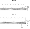
- FIG. 1 is a sectional view of a solar cell according to a comparative example.
- the solar cell 100 includes a semiconductor substrate 10 including a base area 110 and a doping area 120, a doping layer 20 formed on the semiconductor substrate 10 and having a conductive type different from the doping area 120, a tunneling layer 30 interposed between the doping layer 20 and the semiconductor substrate 10, a first electrode 42 connected to the doping area 120, and a second electrode 44 connected to the doping layer 20.
- the base area 110 may have the same conductive type as the doping area 120 and the doping layer 20 may include a material and/or crystalline structure different from the semiconductor substrate 10.
- an anti-reflective film 50 may be further formed on another surface of the semiconductor substrate 10, and a barrier layer 22 may be formed on the doping layer 20. This configuration will be described in more detail.
- the semiconductor substrate 10 includes the base area 110 and the doping area 120 which include an identical first conductive-type dopant.
- the doping area 120 is formed by doping with a high dose of a dopant having the same conductive type as the base area 110.
- a field effect in which movement of undesired carriers towards the doping area 120 is prevented is generated in the doping area 120.
- the doping area 120 corresponds to a back surface field (BSF) region.
- BSF back surface field
- the doping area 120 has the same material, crystalline structure and conductive type as the base area 110, but has a higher doping dose (or dopant concentration) than the base area 110.
- the doping area 120 is formed by preparing a semiconductor substrate 10 including the base area 110 and then doping a portion of the semiconductor substrate 110 with a dopant. Doping methods include a variety of methods such as thermal diffusion or ion implantation. Through at least one of these methods, the semiconductor substrate 10 including the base area 110 and the doping area 120 can be formed.
- a front surface field layer 130 may be entirely formed over the front surface of the semiconductor substrate 10 (that is, over the base area 110).
- the front surface field layer 130 is an area where the first conductive-type dopant is doped at a dose higher than the semiconductor substrate 10 and performs similar functions to the back surface field (BSF) area. That is, the front surface field layer 130 prevents electrons and holes separated by incident sunlight from being recombined and then decayed on the front surface of the semiconductor substrate 10.
- BSF back surface field
- the comparative examples are not limited to this feature, and the front surface field layer 130 may be omitted. This example will be described in more detail with reference to FIG. 9 .
- the base area 110 and the doping area 120 may, for example, include silicon containing a first conductive-type dopant.
- the silicon may be monocrystalline silicon, and the first conductive-type dopant may be, for example, an n-type or p-type dopant. That is, the first conductive-type dopant may be an n-type dopant such as a Group V element including phosphorous (P), arsenic (As), bismuth (Bi), antimony (Sb) or the like. Alternatively, the first conductive-type dopant may be a p-type dopant such as a Group III element including boron (B), aluminum (Al), gallium (Ga), indium (In) or the like.
- the doping layer 20 forming a tunnel junction through the base area 110 and the tunneling layer 30 may have a p-type.
- the doping layer 20 serving as an emitter causing photoelectric transformation through junction with the base area 110 may be widely formed and, as a result, holes having movement speed lower than electrons can be efficiently collected. Electrons created by photoelectric effect are collected by a first electrode 42 when light is emitted to the tunnel junction, and holes are moved toward the front surface of the semiconductor substrate 10 and are then collected by a second electrode 44. As a result, electric energy is generated, but the comparative examples are not limited thereto, and the base area 110 and the doping area 120 may have a p-type while the doping layer 20 may have an n-type.
- the front surface of the semiconductor substrate 10 is textured to have irregularities having a shape such as a pyramidal shape.
- surface roughness is increased due to irregularities formed on the front surface of the semiconductor substrate 10 through such texturing, reflection of light incident through the front surface of the semiconductor substrate 10 can be reduced. Accordingly, an amount of light which reaches the tunnel junction formed by the semiconductor substrate 10 and the doping layer 20 is increased and light loss can thus be minimized.
- the back surface of the semiconductor substrate 10 may be a smooth and even surface having a surface roughness lower than the front surface, obtained through mirror polishing or the like.
- properties of the solar cell 100 may be greatly changed according to properties of the semiconductor substrate 10. For this reason, irregularities obtained by texturing are not formed on the back surface of the semiconductor substrate 10, but the comparative examples are not limited thereto and a variety of modifications are possible.
- an anti-reflective film 50 may be formed on the front surface field layer 130.
- the anti-reflective film 50 may be entirely formed over the front surface of the semiconductor substrate 10.
- the anti-reflective film 50 decreases reflectivity of light incident upon the front surface of the semiconductor substrate 10 and passivates defects present on the surface or in the bulk of the front surface field layer 130.
- the decrease in reflectivity of light incident upon the front surface of the semiconductor substrate 10 causes an increase in an amount of light reaching the tunnel junction. Accordingly, a short current (Isc) of the solar cell 100 can be increased.
- the anti-reflective film 50 passivates defects, removes recombination sites of minority carriers and thus increases an open-circuit voltage (Voc) of the solar cell 100. As such, the anti-reflective film 50 increases the open-circuit voltage and the short current of the solar cell 100, thus improving conversion efficiency of the solar cell 100.
- the anti-reflective film 50 may be formed of a variety of materials.
- the anti-reflective film 50 may be a single film selected from the group consisting of a silicon nitride film, a silicon nitride film containing hydrogen, a silicon oxide film, a silicon oxide nitride film, MgF2, ZnS, TiO2 and CeO2, or a multilayer film including a combination of two or more films, but the comparative examples are not limited thereto and the anti-reflective film 50 may include a variety of materials.
- a tunneling layer 30 is formed on the back surface of the semiconductor substrate 10.
- the tunneling layer 30 improves interface properties of the back surface of the semiconductor substrate 10 and enables produced carriers to be efficiently transferred through a tunneling effect.
- the tunneling layer 30 may include a variety of materials enabling tunneling of carriers and examples of the materials include oxides, nitrides and conductive polymers.
- the tunneling layer 30 may be formed between at least the base area 110 and the doping layer 20.
- the tunneling layer 30 may have a shape corresponding to (that is, substantially the same as) the doping layer 20. Details of the shape will be described in more detail with reference to FIG. 2 .
- the reason for the shape is that the overall process is simplified by etching the tunneling layer 30 and the doping layer 20 in the same process and a doping area 120 is formed through openings 30c and 20c formed in the tunneling layer 30 and the doping layer 20, but the comparative example is not limited thereto. That is, the tunneling layer 30 may be formed in a region other than a region where the doping layer 20 is formed, or in a region corresponding to the doping area 120 as well as the base area 110.
- a thickness of the tunneling layer 30 may be 5.0 nm or less so that the tunneling layer 30 sufficiently exhibits a tunneling effect, or may be 0.5 nm to 5.0 nm (for example, 1.0 nm to 3.0 nm).
- the thickness of the tunneling layer 30 exceeds 5.0 nm, tunneling is not efficiently performed and the solar cell 100 may not operate, and when the thickness of the tunneling layer 30 is less than 0.5 nm, there may be a difficulty in formation of the tunneling layer 30 with desired qualities.
- the thickness of the tunneling layer 30 may be 1.0 nm to 3.0 nm, but the comparative examples are not limited thereto and the thickness of the tunneling layer 30 may be changed.
- the doping layer 20 having a conductive type opposite to the semiconductor substrate 10 is formed on the tunneling layer 30.
- the doping layer 20 may include a semiconductor (for example, silicon) having a second conductive type dopant.
- the doping layer 20 may be formed by doping amorphous silicon, microcrystalline silicon or polycrystalline silicon with a second conductive type dopant by a variety of methods such as deposition or printing.
- the second conductive type dopant may be any dopant having a conductive type opposite to the semiconductor substrate 10. That is, when the second conductive type dopant is a p-type dopant, a Group III element such as boron (B), aluminum (Al), gallium (Ga) or indium (In) may be used.
- the second conductive type dopant is an n-type dopant
- a Group V element such as phosphorus (P), arsenic (As), bismuth (Bi) or antimony (Sb) may be used.
- the doping layer 20 forms a tunnel junction with the base area 110 through the tunneling layer 30, thus substantially contributing to photoelectric transformation.
- the tunneling layer 30 and the doping layer 20 are provided with openings 30c and 20c, respectively, to open regions corresponding to the doping area 120.
- a barrier layer 22 which prevents contamination of the doping layer 20 or the like and aids in formation of the doping area 120 may be disposed on the doping layer 20, when the doping area 120 is formed. Such a barrier layer 22 will be described again with reference to FIGS. 3A to 3G later.
- the barrier layer 22 is not required to be formed and may be not formed according to manufacturing method or the like.
- the first electrode 42 is formed on the semiconductor substrate 10 such that the first electrode 42 is connected to the doping area 120 and the second electrode 44 passes through the barrier layer 22 on the doping layer 20 such that the second electrode 44 is connected to the doping layer 20.
- the first and second electrodes 42 and 44 may include a variety of metal materials.
- the first and second electrodes 42 and 44 may have a variety of plane shapes which are not electrically connected to each other, but are connected to the doping area 120 and the doping layer 20, respectively, to collect produced carriers and transport the same to the outside. That is, the comparative examples are not limited to plane shapes of the first and second electrodes 42 and 44.
- the first electrode 42 is disposed closer to the substrate 10 than the second electrode 44. That is, the first electrode 42 is disposed on the substrate 10 without intervention of at least one of the tunneling layer 30, the doping layer 20 and the barrier layer 22.
- the second electrode 44 is disposed on the substrate 10 with the intervention of at least one of the tunneling layer 30, the doping layer 20. In comparative examples, the second electrode 44 is disposed on the doping layer 20. In another comparative example, the second electrode 44 may be disposed on both of the doping layer 20 and the barrier layer 22.
- the second electrode 44 may be disposed on (for example, directly disposed on) the doping layer 20 inside an opening of the barrier layer 22 (that is, the second electrode 44 may be disposed on (for example, directly disposed on) the doping layer 20 and side surfaces of the opening of the barrier layer 22) and on the barrier layer 22 near the opening of the barrier layer 22.
- the first electrode 42 is recessed relative to the second electrode 44.
- FIG. 2 is a back plane view illustrating the solar cell 100 according to the comparative example..
- the doping area 120 is formed to be narrower than the doping layer 20.
- the tunnel junction formed through the tunneling layer 30 between the semiconductor substrate 110 and the doping layer 20 can be widened.
- the base area 110 and the doping area 120 have an n-conductive type and the doping layer 20 has a p-conductive type, holes having a low movement speed can be efficiently collected.
- the doping area 120 may include a first stem portion 120a formed along a first edge (upper edge in the drawing) of the semiconductor substrate 10 and a plurality of first branch portions 120b which extend from the stem portion 120a toward a second edge (lower edge in the drawing) opposite to the first edge.
- the plurality of first branch portions 120b is aligned to be parallel to each other to have a shape of a stripe pattern.
- the doping layer 20 may include a second stem portion 20a formed along the second edge of the semiconductor substrate 110 and a plurality of second branch portions 20b which extend between the first branch portions 120b toward the first edge from the second stem portion 20a.
- the plurality of second branch portions 20b is aligned to be parallel to each other to have a shape of a stripe pattern.
- the first branch portions 120b of the doping area 120 and the second branch portions 20b of the doping layer 20 may be alternately disposed.
- the tunneling layer 30 may have the same shape as or a similar shape to the doping layer 20 and be thus formed to have portions corresponding to the second stem portion 20a and the second branch portion 20b.
- Areas of the doping area 120 and the doping layer 20 may be controlled by varying widths of the first and second stem portions 120a and 20a and/or the first and second branch portions 120b and 20b. That is, the width of the first stem portion 120a may be smaller than that of the second stem portion 20a, and/or the width of the first branch portion 120b may be smaller than that of the second branch portion 20b.
- a ratio of the total area of the doping area 120 to the total area of the solar cell 100 may be 0.5% to 30% (more preferably 0.5% to 5%).
- the ratio of the total area of the doping area 120 is less than 0.5%, contact between the doping area 120 and the first electrode 42 is not accurately formed and contact resistance between the doping area 120 and the first electrode 42 may thus be increased.
- the area ratio exceeds 30%, the area of the doping layer 20 is decreased and efficiency of the solar cell 100 is thus deteriorated, as described above.
- the area ratio is preferably, but not necessarily, 0.5% to 5% in consideration of efficiency of the solar cell.
- the first electrode 42 may include a stem portion 42a corresponding to the first stem portion 120a of the doping area 120 and a branch portion 42b corresponding to the first branch portion 120b of the doping area 120.
- the second electrode 44 may include a stem portion 44a corresponding to the second stem portion 20a of the doping layer 20 and a branch portion 44b corresponding to the second branch portion 20b of the doping layer 20, but the comparative examples are not limited thereto and the first electrode 42 and the second electrode 44 may have a variety of plane shapes.
- the doping area 120 has the first stem portion 120a
- the doping layer 20 has the second stem portion 20a
- the first electrode 42 has the stem portion 42a
- the second electrode 44 has the stem portion 44a.
- the comparative examples are not limited thereto, and the first and second stem portions 120a and 20a, and the stem portions 42a and 44a are not required. Therefore, one or more of the first stem portions 120a, the second stem portion 20a, the stem portion 42a and stem portion 44a may be not formed or may be not included.
- the first electrode 42 entirely contacts a portion of the doping area 120 where the doping layer 20 is not formed, and the second electrode 44 entirely contacts a portion of the doping area 120 where the doping layer 20 is formed. Accordingly, the region of the doping layer 20 is sufficiently secured, and the doping area 120 and the first electrode 42 are spaced from each other, and the doping layer 20 and the second electrode 44 are spaced from each other. As a result, an electrical connection between the doping area 120 and the first electrode 42 and an electrical connection between the doping layer 20 and the second electrode 44 can be stably formed.
- additional layers for insulating the doping area 120 from the first electrode 42 and for insulating the doping layer 20 from the second electrode 44 are not required and structure and manufacturing process can thus be simplified.
- insulating layers for insulating the doping area 120 from the first electrode 42 and the doping layer 20 from the second electrode 44 to improve insulating properties may be formed.
- the doping area 120 corresponding to the back surface field area which may be formed to have a relatively small area is formed on the semiconductor substrate 10 and the doping layer 20 which needs to have a relatively large area is formed on the tunneling layer 30. Based on this configuration, property or characteristics deterioration and damage of the semiconductor substrate 10, which may be generated during doping of the semiconductor substrate 10 with a dopant, can be efficiently prevented or reduced.
- the doping layer 20 and the doping area 120 are separately formed in areas spaced from each other so that a shunt which may be generated when the doping layer 20 is adjacent to the doping area 120 is prevented. For this reason, open-circuit voltage (Voc) and fill factor of the solar cell 100 are increased and efficiency of the solar cell 100 is thus improved.
- the solar cell 100 according to the comparative example may be formed by a variety of methods and the formation method will be described in more detail with reference to FIGS. 3A to 3G , and FIGS. 4A to 4I .
- FIGS. 3A to 3G are sectional views illustrating a method for manufacturing the solar cell according to a comparative example.
- a semiconductor substrate 10 including a base area 110 having a first conductive-type dopant is prepared in preparation of the substrate.
- the semiconductor substrate 10 may include silicon having an n-type dopant.
- the n-type dopant include Group V elements such as phosphorous (P), arsenic (As), bismuth (Bi) and antimony (Sb).
- the front surface of the semiconductor substrate 10 is textured so that the front surface has irregularities and the back surface of the semiconductor substrate 10 is subjected to treatment such as mirror polishing so that the back surface of the semiconductor substrate 10 has a lower surface roughness than the front surface thereof.
- the back surface may have a flat surface.
- Wet or dry texturing may be used as the texturing of the front surface of the semiconductor substrate 10.
- Wet texturing may be carried out by dipping the semiconductor substrate 10 in a texturing solution and has an advantage of a short process time.
- Dry texturing is a process of cutting the surface of the semiconductor substrate 10 using a diamond drill, laser or the like and enables formation of uniform irregularities, but disadvantageously has a long process time and causes damage to the semiconductor substrate 10.
- the semiconductor substrate 10 may be textured by a reactive ion etching (RIE) or the like.
- RIE reactive ion etching
- the semiconductor substrate 10 may be textured by a variety of methods.
- the back surface of the semiconductor substrate 10 may be treated by a known mirror surface polishing method.
- a tunneling layer 30 and a doping layer 20 are formed on the back surface of the semiconductor substrate 10.
- a barrier layer 22 may be further formed on the doping layer 20.
- the tunneling layer 30 may be formed by a method such as thermal growth or deposition (for example, plasma-enhanced chemical vapor deposition chemical (PECVD), atomic layer deposition (ALD)) or the like, but the comparative examples are not limited thereto and the tunneling layer 30 may be formed by a variety of methods.
- the doping layer 20 includes a microcrystalline, amorphous or polycrystalline semiconductor having a second conductive type dopant.
- the doping layer 20 may be formed by forming a microcrystalline, amorphous or polycrystalline semiconductor by thermal growth, deposition (for example, plasma-enhanced chemical vapor deposition chemical (PECVD)) or the like, and then doping the semiconductor with a second conductive type dopant.
- PECVD plasma-enhanced chemical vapor deposition chemical
- ALD atomic layer deposition
- the doping layer 20 may be formed by doping with the second conductive type dopant while forming a microcrystalline, amorphous or polycrystalline semiconductor through injection of a substance including a second conductive type dopant in the process of thermal growth, deposition (for example, plasma-enhanced chemical vapor deposition chemical (PECVD)) or the like, but the comparative examples are not limited thereto and the semiconductor layer 30 may be formed by a variety of methods.
- PECVD plasma-enhanced chemical vapor deposition chemical
- a mask layer 200 having an opening 200a exposing a region corresponding to the doping area 120 is formed on the doping layer 20.
- the mask layer 200 may be formed by applying a layer including a variety of photoresists, but the comparative examples are not limited thereto and the mask layer 200 may be formed by a variety of methods.
- the doping layer 20, the tunneling layer 30 and the barrier layer 22 are removed from the region corresponding to the opening 200a of the mask layer 200 to form openings 20c and 30c.
- the removal of the doping layer 20 and the tunneling layer 30 of the corresponding region may be carried out using a variety of known methods (for example, etching), but the comparative examples are not limited thereto.
- a doping area 120 is formed in a region corresponding to the openings 20c and 30c by doping a first conductive-type dopant.
- the doping may be carried out using a variety of methods such as ion implantation or thermal diffusion.
- the mask layer 200 may be removed after doping the first conductive-type dopant, but is generally removed after forming the openings 20c and 30c before completion of the formation of the doping area 120 (for example, activated thermal treatment) in order to prevent contamination by the mask layer 200.
- the barrier layer 22 serves as a mask and prevents incorporation of the first conductive-type dopant into the doping layer 20.
- the barrier layer 22 facilitates diffusion of the first conductive-type dopant into the semiconductor substrate 10.
- a front surface field layer 130 is formed on the front surface of the semiconductor substrate 10 and an anti-reflective film 50 is formed thereon.
- the front surface field layer 130 may be formed by doping the semiconductor substrate 10 with a first conductive-type dopant.
- the front surface field layer 130 may be formed by doping the semiconductor substrate 10 with a first conductive-type dopant by a variety of methods such as ion implantation or thermal diffusion.
- the anti-reflective film 50 may be formed by a variety of methods such as vacuum deposition, chemical vapor deposition, spin coating, screen printing or spray coating, but the comparative examples are not limited thereto and various methods may be used.
- first and second electrodes 42 and 44 electrically connected to the doping area 120 and the doping layer 20, respectively, are formed.
- the first electrode 42 is formed by a variety of methods such as coating or deposition after forming an opening in the barrier layer 22.
- the first electrode 42 may be formed by applying a paste for forming the first electrode 42 onto the barrier layer 22 by screen printing or the like and then performing a fire through, a laser firing contact or the like thereon. In this instance, a process of separately forming openings is not required.
- the second electrode 44 may also be formed on the semiconductor substrate 10 (more specifically, on the doping area 120) by a variety of methods such as coating or deposition.
- the tunneling layer 30, the doping layer 20 and the barrier layer 22 are used as masks during formation of the doping area 120, thus advantageously requiring no additional mask process.
- tunneling layer 30, the doping layer 20 and the barrier layer 22 are formed, the doping area 120 is formed, the front surface field layer 130 and the anti-reflective film 50 are formed, and the first and second electrodes 42 and 44 are then formed has been provided in the comparative example above, but the comparative examples are not limited thereto. Accordingly, formation order of the tunneling layer 30, the doping layer 20, the barrier layer 22, the doping area 120, the front surface field layer 130, the anti-reflective film 50, and the first and second electrodes 42 and 44 may be variably changed.
- a method for manufacturing the solar cell 100 according to another comparative example will be described in detail with reference to FIGS. 4A to 4I . Details of the description already given above are not repeated and only difference from the description given above is described in detail.
- FIGS. 4A to 4I are sectional views illustrating a method for manufacturing a solar cell according to another comparative example.
- a semiconductor substrate 10 including a base area 110 having a first conductive-type dopant is prepared in preparation of the substrate.
- a doping area 20 is formed on the back surface of the semiconductor substrate 10 using a mask 202 having an opening 202a.
- the doping area 120 is formed in the area corresponding to the opening 202a by doping a portion of the back surface of the semiconductor substrate 10 with a first conductive-type dopant while the mask 202 is placed on the back surface.
- the mask 202 is placed on the semiconductor substrate 10 and is, for example, a shadow mask.
- a tunneling layer 30 and a doping layer 20 are formed on the back surface of the semiconductor substrate 10.
- a barrier layer 22 may be further formed on the doping layer 20.
- a mask layer 200 having an opening 200a exposing a region corresponding to the doping area 120 is formed on the doping layer 20.
- the doping layer 20, the tunneling layer 30 and the barrier layer 22 are removed from the region corresponding to the opening 200a of the mask layer 200 to form openings 20c and 30c.
- the mask layer 200 is removed.
- a front surface field layer 130 is formed on the front surface of the semiconductor substrate 10 and an anti-reflective film 50 is formed thereon.
- first and second electrodes 42 and 44 electrically connected to the doping area 120 and the doping layer 20, respectively, are formed.
- the solar cell 100 having the structure can be manufactured by a simple process according to the manufacture method of the solar cell 100, but details of the order and the method may be variably changed as described above.
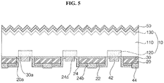
- FIG. 5 is a sectional view illustrating a solar cell according to another comparative example and FIG. 6 is a back plan view illustrating the solar cell shown in the FIG. 5 .
- the insulating layer 24 is not shown in FIG. 6 .
- the doping area 120 of the comparative example includes a plurality of first portions 120c connected to the first electrode 42, and the first portions 120c have an island shape.
- an area of the doping area 120 is minimized and the doping area 120 is entirely disposed over the semiconductor substrate 10. That is, surface recombination can be prevented or reduced and an area of the doping layer 20 can be maximized, and the doping area 120 may have a variety of shapes capable of minimizing the area of the doping area 120.
- the doping area 120 having a circular shape is shown in the drawing by example. Accordingly, the doping area 120 may have a plane shape including an oval or a polygon, for example, a triangle, rectangle or hexagon.
- a width or diameter of the doping area 120 may be 50 ⁇ m to 1,000 ⁇ m.
- the width or diameter of the doping area 120 is less than 50 ⁇ m, electrical connection between the doping area 120 and the first electrode 42 may not be efficient and when the width or diameter thereof exceeds 1,000 ⁇ m, the area of the doping layer 20 may be decreased or a pitch between the doping area 120 may be increased.
- the width or diameter of the doping area 120 may be 100 ⁇ m to 500 ⁇ m.
- the doping layer 20 may have an entirely connected to have an integral structure and include an opening (or openings) 20d formed in a region corresponding to the first region 120c. Similar to this, the tunneling layer 30 includes openings 30d corresponding to the first regions 120c and the openings 20d, and the tunneling layer 30 except for the openings 30d is continuously connected between the doping layer and the semiconductor substrate is continuously connected to have an integral structure. When present, the barrier layer 22 may also have an opening in the corresponding region. The openings 20d and 30d of the doping layer 20 and the tunneling layer 30 may be wider than the first region 120c and the first region 120c may be entirely disposed in the openings 20d and 30d.
- An insulating layer 24 for insulating the doping area 120 from the doping layer 20 may be formed on the semiconductor substrate 10 including the doping area 120 and the doping layer 20 (or barrier layer 22).
- a first contact hole 24a for connecting the first electrode 42 to the first region 120c of the doping area 120, and a second contact hole 24b for connecting the second electrode 44 to the doping layer 20 may be formed in the insulating layer 24.
- the first contact hole 24a may be formed to have an island shape in a region that corresponds to the first region 120c and the second contact hole 24b may have a shape entirely the same as or similar to the second electrode 44 according to the shape of the second electrode 44.
- the second contact hole 24b may have portions corresponding to the stem portion 44a and the branch portion 44b.
- the first contact hole 24a and the second contact hole 24b may have different shapes in consideration of the doping area 120 having an island region and the entirely connected shape of the doping layer 20.
- electrical connection of the first electrode 42 and the doping area 120 having an island shape is efficiently secured, and insulation between the first electrode 42 and the doping layer 20 is stably maintained.
- the second electrode 44 entirely contacts the doping layer 20, thereby improving carrier resin efficiency, and shapes of the first and second contact holes 24a and 24b may be changed.
- first electrode 42 has the same shape as in the embodiment shown in FIG. 1 has been given in the comparative example, but the shape of the first electrode 42 or the like may be varied. A modified embodiment will be described with reference to FIG. 7 .
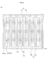
- FIG. 7 is a back plan view illustrating a solar cell according to the embodiment of the invention.
- the branch portion 42b of the first electrode 42 includes a plurality of first portions 421b corresponding to the first region 120c of the doping area 120, and a second portion 422b which connects the first portions 421b to one another and has a smaller width than each first portion 421b. That is, the width of the first portion 421b corresponding to the first region 120c is greater than widths of other portions, thereby sufficiently securing areas of the respective first portions 120c, or areas of contact holes 24 connecting the first electrode 42 to the first region 120c. As a result, electrical connection between the first electrode 42 and the first region 120c is further facilitated.
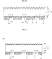
- FIGS. 8A to 8C are sectional views illustrating a method for manufacturing a solar cell according to the embodiment of the invention.
- a doping area 120 is formed on the semiconductor substrate 10 and a tunneling layer 30, a doping layer 20 and a barrier layer 22 having openings 30d and 20d are formed on the semiconductor substrate 10.
- an insulating layer 24 is formed over the entire surface of the structure including the semiconductor substrate 10, the tunneling layer 30, the doping layer 20 and the barrier layer 22.
- the insulating layer 24 may include a variety of insulating materials (for example, oxides, nitrides or the like) and may be formed by a variety of methods such as vacuum deposition, chemical vapor deposition, spin coating, screen printing or spray coating, but the embodiments of the invention are not limited thereto and various methods may be used.
- a front surface field layer 130 and an anti-reflective film 50 are formed on the front surface of the semiconductor substrate 110.
- first and second electrodes 42 and 44 electrically connected to the doping area 120 and the doping layer 20 through a first contact hole 24a and a second contact hole 24b are formed.
- the solar cell 100 having the structure described above can be formed by such a manufacturing method.
- FIG. 9 is a sectional view illustrating a solar cell according to still another comparative example.
- the semiconductor substrate 10 includes only the base area 110 and does not include an additional front surface field layer (represented by reference numeral "130" in FIG. 1 , the same will be applied below). Instead, a field effect-forming layer 52 which contacts the base area 110 of the semiconductor substrate 10 and has a fixed charge is formed. Similar to the front surface field layer 130, the field effect-forming layer 52 generates a certain field effect and thereby prevents or reduces surface recombination.
- the field effect-forming layer 52 may be composed of aluminum oxide having a negative charge, or silicon oxide or silicon nitride having a positive charge or the like.
- an additional anti-reflective film represented by reference numeral "50" in FIG. 1 ) may be further formed on the field effect-forming layer 52.
- the area of the doping area formed in the semiconductor substrate 10 is greatly reduced and the overall process is thus simplified.
- damage to the semiconductor substrate 10 which may be generated during formation of the doping area can be efficiently reduced.
- an amount of fixed charges of the field effect-forming layer 52 is for example, 1 X 10¹²/cm 2 to 9 X 10¹³ /cm 2 .
- the amount of the fixed charges is a level enabling generation of the field effect in the semiconductor substrate 10 not including the doping area. More specifically, in consideration of the field effect, the amount of fixed charges may be 1 X 10 12 /cm 2 to 1 X 10 13 /cm 2 , but the comparative example is not limited thereto and the amount of fixed charges may be varied.
- the base area 110 not including the doping area may have a specific resistance of 0.5 ohm ⁇ cm to 20 ohm ⁇ cm (for example, 1 ohm ⁇ cm to 15 ohm ⁇ cm). Accordingly, in a region adjacent to the field effect-forming layer 52, the semiconductor substrate 10 may have a specific resistance of 0.5 ohm ⁇ cm to 20 ohm ⁇ cm (for example, 1 ohm ⁇ cm to 15 ohm ⁇ cm).
- this specific resistance range is given as an example of an instance when the semiconductor substrate 10 includes an n-type base area 110 using phosphorous (P) as a dopant and may be changed according to conductive type, dopant type or the like.
Landscapes
- Engineering & Computer Science (AREA)
- Life Sciences & Earth Sciences (AREA)
- Computer Hardware Design (AREA)
- Physics & Mathematics (AREA)
- Condensed Matter Physics & Semiconductors (AREA)
- Electromagnetism (AREA)
- General Physics & Mathematics (AREA)
- Microelectronics & Electronic Packaging (AREA)
- Power Engineering (AREA)
- Sustainable Energy (AREA)
- Sustainable Development (AREA)
- Manufacturing & Machinery (AREA)
- Crystallography & Structural Chemistry (AREA)
- Chemical & Material Sciences (AREA)
- Photovoltaic Devices (AREA)
Claims (12)
- Cellule solaire (100) comprenant :un substrat à semi-conducteur (10) comprenant une zone de base (110) et une zone de dopage (120), la zone de base et la zone de dopage (120c) ayant un dopant de premier type de conductivité, la zone de dopage ayant une concentration en dopant supérieure à celle de la zone de base ;une couche de dopage (20) disposée sur le substrat semi-conducteur (10), la couche de dopage (20) ayant un second type conducteur opposé au premier type de conductivité, la couche de dopage et la zone de dopage étant disposées sur une face du substrat ;une couche à effet tunnel (30) intercalée entre la couche de dopage (20) et le substrat à semi-conducteur (10) ;une couche isolante (24) disposée tout le long de ladite face du substrat, sur la zone de dopage et sur la couche de dopage ;une première électrode (42) disposée sur la couche isolante (24) et connectée à la zone de dopage (120) ; etune seconde électrode (44) disposée sur la couche isolante (24) et connectée à la couche de dopage (20),la zone de dopage (120) comprenant une pluralité de zones dopées (120c) ayant une forme d'ilot et étant séparées les unes des autres ;chaque zone dopée de la pluralité des zones dopées (120c) étant espacée de la couche dopée par une partie de la zone de base (110) ;la première électrode (42) comprenant une pluralité de premières parties (421b) et une seconde partie (422b), la pluralité des premières parties (421b) étant connectées à la pluralité de zones dopées (120c), et la seconde partie (422b) étant conçue pour connecté les premières parties (241b) les unes aux autres ; etcaractérisée en ce qu'une largeur de la seconde partie (422b) de la première électrode étant inférieure à une largeur de chacune des premières parties (421b) de la première électrode,la couche isolante (24) recouvrant chaque partie de la zone de base disposée entre chacune zone dopée de la pluralité de zones dopées et la couche dopée.
- Cellule solaire (100) selon la revendication 1, comprenant en outre :un premier trou de contact (24a) formé dans la couche isolante (24) et conçu pour connecter la première électrode (42) aux zones dopées (120c), etun second trou de contact (24b) formé dans la couche isolante (24) et conçu pour connecter la seconde électrode (44) à la couche de dopage (20).
- Cellule solaire (100) selon la revendication 1, une structure cristalline de la couche de dopage (20) étant différente d'une structure cristalline du substrat à semi-conducteur (10).
- Cellule solaire (100) selon la revendication 3, le substrat à semi-conducteur (10) ayant une structure monocristalline, et la couche de dopage (20) ayant une structure microcristalline ou polycristalline amorphe.
- Cellule solaire (100) selon la revendication 3, la zone de base (110) et la zone de dopage (120) étant de type n et la couche de dopage (20) de type p.
- Cellule solaire (100) selon la revendication 1, une épaisseur de la couche de dopage (20) étant supérieure à une épaisseur de la couche à effet tunnel (30).
- Cellule solaire (100) selon la revendication 1, au moins l'une des conditions suivantes étant remplie :la couche à effet tunnel (30) comprenant des ouvertures (30a, 30a) correspondant à la pluralité de zones dopées (120c) espacées de la couche à effet tunnel (30) sur chacune de leurs faces par la partie de la zone de base recouverte par la couche isolante, et la couche à effet tunnel (30) étant connectée en continu, sauf au niveau des ouvertures (30c) entre la couche de dopage (20) et le substrat à semi-conducteur (10) comprenant la couche isolante recouvrant les parois latérales de la couche à effet tunnel pour avoir une structure intégrale ; etla couche de dopage (20) comprenant des ouvertures (20a, 20d) correspondant à la pluralité des zones dopées (120c) espacées de la couche à effet tunnel (30) sur chacune de leurs faces par la partie de zone de base recouverte par la couche isolante, et la couche de dopage (20) étant connectée en continu, sauf au niveau des ouvertures (20c) comprenant la couche isolante recouvrant les parois latérales de la couche dopée pour avoir une structure intégrale.
- Cellule solaire (100) selon la revendication 1, la couche à effet tunnel (30) ayant une forme correspondant à la couche de dopage (20).
- Procédé de fabrication d'une cellule solaire (100) comprenant une zone de base (110) et une zone de dopage (120), le procédé consistant à :préparer un substrat à semi-conducteur (10) ;former une couche à effet tunnel (30) sur une surface du substrat à semi-conducteur (10) ;former une couche de dopage (20) sur la couche à effet tunnel (30) ;doper le substrat à semi-conducteur (10) à l'aide d'un dopant pour former la zone de dopage (120), la zone de base et la zone de dopage (120c) ayant un dopant de premier type de conductivité, la zone de dopage ayant une concentration en dopant supérieure à celle de la zone de base et la couche de dopage (20) ayant un second type de conductivité opposé au premier type de conductivité ;former une couche isolante (24) disposée toute le long de ladite face du substrat, sur la zone de dopage et sur la couche de dopage ;former une première électrode (42) disposée sur la couche isolante et une seconde électrode (44) disposée sur la couche isolante et connectée à la zone de dopage (120) et la couche de dopage (20), respectivement, etla zone de dopage (120) comprenant une pluralité de zones dopées (120c), chaque zone dopée (120c) de la pluralité de zones dopées (120c) ayant une forme d'ilot et étant séparée les unes des autres,chacune zone dopée de la pluralité des zones dopées (120c) étant espacée de la couche dopée par une partie de la zone de base (110) ; etla première électrode (42) comprenant une pluralité de premières parties (421b) et une seconde partie (422b), la pluralité des premières parties (421b) étant connectées à la pluralité de zones dopées (120c), la seconde partie (422b) étant conçue pour connecter les premières parties (421b) les unes aux autres ;caractérisée en ce qu'une largeur de la seconde partie (422b) de la première électrode étant inférieure à une largeur de chacune des premières parties (421b) de la première électrode, et
la couche isolante (24) recouvre chaque partie de la zone de base disposée entre chaque zone dopée de la pluralité de zones dopées et la couche dopée. - Procédé selon la revendication 9, consistant en outre à :former un premier trou de contact (24a) dans la couche isolante (24) pour connecter la première électrode (42) aux zones dopées (120c), etformer un second trou de contact (24b) dans la couche isolante (24) pour connecter la seconde électrode (44) à la couche de dopage (20).
- Procédé selon la revendication 9, consistant en outre à :
former des motifs sur la couche à effet tunnel (30) et la couche de dopage (20) pour former des ouvertures (20c, 30c) après la formation de la couche de dopage (20) et avant la formation de la zone de dopage (120). - Procédé selon la revendication 9, la formation de la zone de dopage (120) ayant lieu avant la formation de la couche à effet tunnel (30), et la formation de la zone de dopage (120) consistant à doper la surface du substrat à semi-conducteur (10) avec du dopant à l'aide d'un masque.
Applications Claiming Priority (1)
| Application Number | Priority Date | Filing Date | Title |
|---|---|---|---|
| KR1020130055756A KR20140135881A (ko) | 2013-05-16 | 2013-05-16 | 태양 전지 및 이의 제조 방법 |
Publications (2)
| Publication Number | Publication Date |
|---|---|
| EP2804219A1 EP2804219A1 (fr) | 2014-11-19 |
| EP2804219B1 true EP2804219B1 (fr) | 2019-10-16 |
Family
ID=50732751
Family Applications (1)
| Application Number | Title | Priority Date | Filing Date |
|---|---|---|---|
| EP14001746.8A Active EP2804219B1 (fr) | 2013-05-16 | 2014-05-16 | Cellule solaire et son procédé de fabrication |
Country Status (4)
| Country | Link |
|---|---|
| US (1) | US10566484B2 (fr) |
| EP (1) | EP2804219B1 (fr) |
| KR (1) | KR20140135881A (fr) |
| CN (1) | CN104167454B (fr) |
Families Citing this family (20)
| Publication number | Priority date | Publication date | Assignee | Title |
|---|---|---|---|---|
| DE102013100818B4 (de) * | 2013-01-28 | 2023-07-27 | OSRAM Opto Semiconductors Gesellschaft mit beschränkter Haftung | Optoelektronischer Halbleiterchip und Verfahren zur Herstellung eines optoelektronischen Halbleiterchips |
| CN104282788B (zh) * | 2014-09-28 | 2017-03-22 | 苏州中来光伏新材股份有限公司 | 无主栅、高效率背接触太阳能电池模块、组件及制备工艺 |
| KR102317141B1 (ko) * | 2015-02-10 | 2021-10-22 | 엘지전자 주식회사 | 태양 전지 |
| KR102373649B1 (ko) * | 2015-05-28 | 2022-03-11 | 엘지전자 주식회사 | 태양 전지 및 이의 제조 방법 |
| NL2015533B1 (en) * | 2015-09-30 | 2017-04-20 | Tempress Ip B V | Method of manufacturing of a solar cell and solar cell thus obtained. |
| CN109074895B (zh) | 2016-08-16 | 2022-05-27 | 浙江凯盈新材料有限公司 | 用于硅太阳能电池中正面金属化的厚膜浆料 |
| NL2017872B1 (en) * | 2016-11-25 | 2018-06-08 | Stichting Energieonderzoek Centrum Nederland | Photovoltaic cell with passivating contact |
| SG11201809794SA (en) | 2016-12-20 | 2018-12-28 | Zhejiang Kaiying New Materials Co Ltd | Interdigitated back contact metal-insulator-semiconductor solar cell with printed oxide tunnel junctions |
| MY189222A (en) | 2016-12-20 | 2022-01-31 | Zhejiang Kaiying New Mat Co Ltd | Siloxane-containing solar cell metallization pastes |
| CN111108609A (zh) * | 2017-09-22 | 2020-05-05 | 荷兰应用自然科学研究组织Tno | 具有p型导电性的指叉背接触式太阳能电池 |
| CN108666377A (zh) * | 2018-07-11 | 2018-10-16 | 泰州隆基乐叶光伏科技有限公司 | 一种p型背接触太阳电池及其制备方法 |
| JP7346050B2 (ja) * | 2019-03-26 | 2023-09-19 | パナソニックホールディングス株式会社 | 太陽電池セルおよび太陽電池モジュール |
| CN110061086A (zh) * | 2019-04-04 | 2019-07-26 | 国家电投集团西安太阳能电力有限公司 | 一种hbc太阳能电池 |
| US10622502B1 (en) | 2019-05-23 | 2020-04-14 | Zhejiang Kaiying New Materials Co., Ltd. | Solar cell edge interconnects |
| US10749045B1 (en) | 2019-05-23 | 2020-08-18 | Zhejiang Kaiying New Materials Co., Ltd. | Solar cell side surface interconnects |
| DE102019122637B4 (de) * | 2019-08-22 | 2022-11-03 | Fraunhofer-Gesellschaft zur Förderung der angewandten Forschung e.V. | Verfahren zur Herstellung einer metallischen Kontaktierungsstruktur einer photovoltaischen Solarzelle |
| US11824126B2 (en) * | 2019-12-10 | 2023-11-21 | Maxeon Solar Pte. Ltd. | Aligned metallization for solar cells |
| DE102020111997A1 (de) * | 2020-05-04 | 2021-11-04 | EnPV GmbH | Rückseitenkontaktierte Solarzelle |
| DE102020132245A1 (de) * | 2020-12-04 | 2022-06-09 | EnPV GmbH | Rückseitenkontaktierte Solarzelle und Herstellung einer solchen |
| CN114361268A (zh) * | 2021-12-29 | 2022-04-15 | 中国建材国际工程集团有限公司 | 一种背接触CdTe太阳电池及其制造方法 |
Citations (4)
| Publication number | Priority date | Publication date | Assignee | Title |
|---|---|---|---|---|
| EP2395554A2 (fr) * | 2010-06-14 | 2011-12-14 | Imec | Procédé de fabrication pour cellules photovoltaïques à contact arrière interdigité |
| US20120037224A1 (en) * | 2009-04-29 | 2012-02-16 | Mitsubishi Electric Corporation | Solar battery cell and method of manufacturing the same |
| WO2012173480A2 (fr) * | 2011-06-14 | 2012-12-20 | Stichting Energieonderzoek Centrum Nederland | Pile photovoltaïque |
| CN102856328A (zh) * | 2012-10-10 | 2013-01-02 | 友达光电股份有限公司 | 太阳能电池及其制作方法 |
Family Cites Families (14)
| Publication number | Priority date | Publication date | Assignee | Title |
|---|---|---|---|---|
| US4496788A (en) * | 1982-12-29 | 1985-01-29 | Osaka Transformer Co., Ltd. | Photovoltaic device |
| JP3203078B2 (ja) * | 1992-12-09 | 2001-08-27 | 三洋電機株式会社 | 光起電力素子 |
| US6111189A (en) * | 1998-07-28 | 2000-08-29 | Bp Solarex | Photovoltaic module framing system with integral electrical raceways |
| JP3490964B2 (ja) * | 2000-09-05 | 2004-01-26 | 三洋電機株式会社 | 光起電力装置 |
| CN100401532C (zh) * | 2001-11-26 | 2008-07-09 | 壳牌阳光有限公司 | 太阳能电池及其制造方法 |
| WO2009096539A1 (fr) * | 2008-01-30 | 2009-08-06 | Kyocera Corporation | Élément de batterie solaire et procédé de fabrication d'élément de batterie solaire |
| DE102009024598A1 (de) | 2009-06-10 | 2011-01-05 | Institut Für Solarenergieforschung Gmbh | Solarzelle mit Kontaktstruktur mit geringen Rekombinationsverlusten sowie Herstellungsverfahren für solche Solarzellen |
| US8735234B2 (en) * | 2010-02-18 | 2014-05-27 | Varian Semiconductor Equipment Associates, Inc. | Self-aligned ion implantation for IBC solar cells |
| KR20130056364A (ko) * | 2010-04-23 | 2013-05-29 | 솔렉셀, 인크. | 고효율 태양 전지 극 저 표면 재결합 속도를 달성하기 위한 패시베이션 방법 및 장치 |
| KR101773837B1 (ko) * | 2011-01-21 | 2017-09-01 | 엘지전자 주식회사 | 태양전지 및 그 제조방법 |
| KR20120086593A (ko) | 2011-01-26 | 2012-08-03 | 엘지전자 주식회사 | 태양전지 및 그 제조방법 |
| KR20120129264A (ko) | 2011-05-19 | 2012-11-28 | 삼성디스플레이 주식회사 | 태양 전지 및 이의 제조방법 |
| US9112086B2 (en) | 2011-11-10 | 2015-08-18 | Semiconductor Energy Laboratory Co., Ltd. | Photoelectric conversion device |
| JP2015133341A (ja) | 2012-04-27 | 2015-07-23 | パナソニック株式会社 | 裏面接合型太陽電池及びその製造方法 |
-
2013
- 2013-05-16 KR KR1020130055756A patent/KR20140135881A/ko active Application Filing
-
2014
- 2014-05-15 US US14/278,827 patent/US10566484B2/en active Active
- 2014-05-16 CN CN201410354042.5A patent/CN104167454B/zh not_active Expired - Fee Related
- 2014-05-16 EP EP14001746.8A patent/EP2804219B1/fr active Active
Patent Citations (5)
| Publication number | Priority date | Publication date | Assignee | Title |
|---|---|---|---|---|
| US20120037224A1 (en) * | 2009-04-29 | 2012-02-16 | Mitsubishi Electric Corporation | Solar battery cell and method of manufacturing the same |
| EP2395554A2 (fr) * | 2010-06-14 | 2011-12-14 | Imec | Procédé de fabrication pour cellules photovoltaïques à contact arrière interdigité |
| WO2012173480A2 (fr) * | 2011-06-14 | 2012-12-20 | Stichting Energieonderzoek Centrum Nederland | Pile photovoltaïque |
| CN102856328A (zh) * | 2012-10-10 | 2013-01-02 | 友达光电股份有限公司 | 太阳能电池及其制作方法 |
| US20140096821A1 (en) * | 2012-10-10 | 2014-04-10 | Au Optronics Corp. | Solar cell and method for making thereof |
Also Published As
| Publication number | Publication date |
|---|---|
| CN104167454A (zh) | 2014-11-26 |
| EP2804219A1 (fr) | 2014-11-19 |
| KR20140135881A (ko) | 2014-11-27 |
| US20140338747A1 (en) | 2014-11-20 |
| US10566484B2 (en) | 2020-02-18 |
| CN104167454B (zh) | 2017-10-13 |
Similar Documents
| Publication | Publication Date | Title |
|---|---|---|
| EP2804219B1 (fr) | Cellule solaire et son procédé de fabrication | |
| US11329172B2 (en) | Solar cell | |
| EP2822041B1 (fr) | Cellule solaire et son procédé de fabrication | |
| US10854764B2 (en) | Solar cell and method for manufacturing the same | |
| EP2879189B1 (fr) | Cellule solaire et son procédé de fabrication | |
| EP2988336B1 (fr) | Cellule solaire et son procédé de fabrication | |
| US10424681B2 (en) | Solar cell | |
| KR102244838B1 (ko) | 태양 전지 및 이의 제조 방법 | |
| US20130160840A1 (en) | Solar cell | |
| KR20150049211A (ko) | 태양 전지 및 이의 제조 방법 | |
| KR102053140B1 (ko) | 태양 전지 | |
| KR102132741B1 (ko) | 태양 전지 및 이의 제조 방법 | |
| KR102298671B1 (ko) | 태양 전지 및 이의 제조 방법 | |
| KR102082880B1 (ko) | 태양 전지의 제조 방법 | |
| KR20160061947A (ko) | 태양 전지 및 이의 제조 방법 | |
| KR20150049213A (ko) | 태양 전지 |
Legal Events
| Date | Code | Title | Description |
|---|---|---|---|
| PUAI | Public reference made under article 153(3) epc to a published international application that has entered the european phase |
Free format text: ORIGINAL CODE: 0009012 |
|
| 17P | Request for examination filed |
Effective date: 20140516 |
|
| AK | Designated contracting states |
Kind code of ref document: A1 Designated state(s): AL AT BE BG CH CY CZ DE DK EE ES FI FR GB GR HR HU IE IS IT LI LT LU LV MC MK MT NL NO PL PT RO RS SE SI SK SM TR |
|
| AX | Request for extension of the european patent |
Extension state: BA ME |
|
| STAA | Information on the status of an ep patent application or granted ep patent |
Free format text: STATUS: EXAMINATION IS IN PROGRESS |
|
| 17Q | First examination report despatched |
Effective date: 20170109 |
|
| REG | Reference to a national code |
Ref country code: DE Ref legal event code: R079 Ref document number: 602014055124 Country of ref document: DE Free format text: PREVIOUS MAIN CLASS: H01L0031022400 Ipc: H01L0031068000 |
|
| GRAJ | Information related to disapproval of communication of intention to grant by the applicant or resumption of examination proceedings by the epo deleted |
Free format text: ORIGINAL CODE: EPIDOSDIGR1 |
|
| STAA | Information on the status of an ep patent application or granted ep patent |
Free format text: STATUS: GRANT OF PATENT IS INTENDED |
|
| RIC1 | Information provided on ipc code assigned before grant |
Ipc: H01L 31/0747 20120101ALI20190416BHEP Ipc: H01L 31/068 20120101AFI20190416BHEP Ipc: H01L 31/0224 20060101ALI20190416BHEP Ipc: H01L 31/18 20060101ALI20190416BHEP |
|
| GRAP | Despatch of communication of intention to grant a patent |
Free format text: ORIGINAL CODE: EPIDOSNIGR1 |
|
| INTG | Intention to grant announced |
Effective date: 20190529 |
|
| RIN1 | Information on inventor provided before grant (corrected) |
Inventor name: PARK, HYUNJUNG Inventor name: CHOE, YOUNGHO Inventor name: CHOI, MINHO Inventor name: CHOI, JUNGHOON |
|
| GRAS | Grant fee paid |
Free format text: ORIGINAL CODE: EPIDOSNIGR3 |
|
| GRAA | (expected) grant |
Free format text: ORIGINAL CODE: 0009210 |
|
| STAA | Information on the status of an ep patent application or granted ep patent |
Free format text: STATUS: THE PATENT HAS BEEN GRANTED |
|
| AK | Designated contracting states |
Kind code of ref document: B1 Designated state(s): AL AT BE BG CH CY CZ DE DK EE ES FI FR GB GR HR HU IE IS IT LI LT LU LV MC MK MT NL NO PL PT RO RS SE SI SK SM TR |
|
| REG | Reference to a national code |
Ref country code: GB Ref legal event code: FG4D |
|
| REG | Reference to a national code |
Ref country code: CH Ref legal event code: EP |
|
| REG | Reference to a national code |
Ref country code: DE Ref legal event code: R096 Ref document number: 602014055124 Country of ref document: DE |
|
| REG | Reference to a national code |
Ref country code: IE Ref legal event code: FG4D |
|
| REG | Reference to a national code |
Ref country code: AT Ref legal event code: REF Ref document number: 1192141 Country of ref document: AT Kind code of ref document: T Effective date: 20191115 |
|
| REG | Reference to a national code |
Ref country code: NL Ref legal event code: MP Effective date: 20191016 |
|
| REG | Reference to a national code |
Ref country code: LT Ref legal event code: MG4D |
|
| REG | Reference to a national code |
Ref country code: AT Ref legal event code: MK05 Ref document number: 1192141 Country of ref document: AT Kind code of ref document: T Effective date: 20191016 |
|
| PG25 | Lapsed in a contracting state [announced via postgrant information from national office to epo] |
Ref country code: NL Free format text: LAPSE BECAUSE OF FAILURE TO SUBMIT A TRANSLATION OF THE DESCRIPTION OR TO PAY THE FEE WITHIN THE PRESCRIBED TIME-LIMIT Effective date: 20191016 Ref country code: AT Free format text: LAPSE BECAUSE OF FAILURE TO SUBMIT A TRANSLATION OF THE DESCRIPTION OR TO PAY THE FEE WITHIN THE PRESCRIBED TIME-LIMIT Effective date: 20191016 Ref country code: BG Free format text: LAPSE BECAUSE OF FAILURE TO SUBMIT A TRANSLATION OF THE DESCRIPTION OR TO PAY THE FEE WITHIN THE PRESCRIBED TIME-LIMIT Effective date: 20200116 Ref country code: FI Free format text: LAPSE BECAUSE OF FAILURE TO SUBMIT A TRANSLATION OF THE DESCRIPTION OR TO PAY THE FEE WITHIN THE PRESCRIBED TIME-LIMIT Effective date: 20191016 Ref country code: LT Free format text: LAPSE BECAUSE OF FAILURE TO SUBMIT A TRANSLATION OF THE DESCRIPTION OR TO PAY THE FEE WITHIN THE PRESCRIBED TIME-LIMIT Effective date: 20191016 Ref country code: PT Free format text: LAPSE BECAUSE OF FAILURE TO SUBMIT A TRANSLATION OF THE DESCRIPTION OR TO PAY THE FEE WITHIN THE PRESCRIBED TIME-LIMIT Effective date: 20200217 Ref country code: SE Free format text: LAPSE BECAUSE OF FAILURE TO SUBMIT A TRANSLATION OF THE DESCRIPTION OR TO PAY THE FEE WITHIN THE PRESCRIBED TIME-LIMIT Effective date: 20191016 Ref country code: LV Free format text: LAPSE BECAUSE OF FAILURE TO SUBMIT A TRANSLATION OF THE DESCRIPTION OR TO PAY THE FEE WITHIN THE PRESCRIBED TIME-LIMIT Effective date: 20191016 Ref country code: NO Free format text: LAPSE BECAUSE OF FAILURE TO SUBMIT A TRANSLATION OF THE DESCRIPTION OR TO PAY THE FEE WITHIN THE PRESCRIBED TIME-LIMIT Effective date: 20200116 Ref country code: GR Free format text: LAPSE BECAUSE OF FAILURE TO SUBMIT A TRANSLATION OF THE DESCRIPTION OR TO PAY THE FEE WITHIN THE PRESCRIBED TIME-LIMIT Effective date: 20200117 Ref country code: PL Free format text: LAPSE BECAUSE OF FAILURE TO SUBMIT A TRANSLATION OF THE DESCRIPTION OR TO PAY THE FEE WITHIN THE PRESCRIBED TIME-LIMIT Effective date: 20191016 |
|
| PG25 | Lapsed in a contracting state [announced via postgrant information from national office to epo] |
Ref country code: RS Free format text: LAPSE BECAUSE OF FAILURE TO SUBMIT A TRANSLATION OF THE DESCRIPTION OR TO PAY THE FEE WITHIN THE PRESCRIBED TIME-LIMIT Effective date: 20191016 Ref country code: HR Free format text: LAPSE BECAUSE OF FAILURE TO SUBMIT A TRANSLATION OF THE DESCRIPTION OR TO PAY THE FEE WITHIN THE PRESCRIBED TIME-LIMIT Effective date: 20191016 Ref country code: IS Free format text: LAPSE BECAUSE OF FAILURE TO SUBMIT A TRANSLATION OF THE DESCRIPTION OR TO PAY THE FEE WITHIN THE PRESCRIBED TIME-LIMIT Effective date: 20200224 |
|
| PG25 | Lapsed in a contracting state [announced via postgrant information from national office to epo] |
Ref country code: AL Free format text: LAPSE BECAUSE OF FAILURE TO SUBMIT A TRANSLATION OF THE DESCRIPTION OR TO PAY THE FEE WITHIN THE PRESCRIBED TIME-LIMIT Effective date: 20191016 |
|
| REG | Reference to a national code |
Ref country code: DE Ref legal event code: R097 Ref document number: 602014055124 Country of ref document: DE |
|
| PG2D | Information on lapse in contracting state deleted |
Ref country code: IS |
|
| PG25 | Lapsed in a contracting state [announced via postgrant information from national office to epo] |
Ref country code: RO Free format text: LAPSE BECAUSE OF FAILURE TO SUBMIT A TRANSLATION OF THE DESCRIPTION OR TO PAY THE FEE WITHIN THE PRESCRIBED TIME-LIMIT Effective date: 20191016 Ref country code: CZ Free format text: LAPSE BECAUSE OF FAILURE TO SUBMIT A TRANSLATION OF THE DESCRIPTION OR TO PAY THE FEE WITHIN THE PRESCRIBED TIME-LIMIT Effective date: 20191016 Ref country code: ES Free format text: LAPSE BECAUSE OF FAILURE TO SUBMIT A TRANSLATION OF THE DESCRIPTION OR TO PAY THE FEE WITHIN THE PRESCRIBED TIME-LIMIT Effective date: 20191016 Ref country code: EE Free format text: LAPSE BECAUSE OF FAILURE TO SUBMIT A TRANSLATION OF THE DESCRIPTION OR TO PAY THE FEE WITHIN THE PRESCRIBED TIME-LIMIT Effective date: 20191016 Ref country code: DK Free format text: LAPSE BECAUSE OF FAILURE TO SUBMIT A TRANSLATION OF THE DESCRIPTION OR TO PAY THE FEE WITHIN THE PRESCRIBED TIME-LIMIT Effective date: 20191016 Ref country code: IS Free format text: LAPSE BECAUSE OF FAILURE TO SUBMIT A TRANSLATION OF THE DESCRIPTION OR TO PAY THE FEE WITHIN THE PRESCRIBED TIME-LIMIT Effective date: 20200216 |
|
| PLBE | No opposition filed within time limit |
Free format text: ORIGINAL CODE: 0009261 |
|
| STAA | Information on the status of an ep patent application or granted ep patent |
Free format text: STATUS: NO OPPOSITION FILED WITHIN TIME LIMIT |
|
| PG25 | Lapsed in a contracting state [announced via postgrant information from national office to epo] |
Ref country code: SM Free format text: LAPSE BECAUSE OF FAILURE TO SUBMIT A TRANSLATION OF THE DESCRIPTION OR TO PAY THE FEE WITHIN THE PRESCRIBED TIME-LIMIT Effective date: 20191016 Ref country code: SK Free format text: LAPSE BECAUSE OF FAILURE TO SUBMIT A TRANSLATION OF THE DESCRIPTION OR TO PAY THE FEE WITHIN THE PRESCRIBED TIME-LIMIT Effective date: 20191016 Ref country code: IT Free format text: LAPSE BECAUSE OF FAILURE TO SUBMIT A TRANSLATION OF THE DESCRIPTION OR TO PAY THE FEE WITHIN THE PRESCRIBED TIME-LIMIT Effective date: 20191016 |
|
| 26N | No opposition filed |
Effective date: 20200717 |
|
| PG25 | Lapsed in a contracting state [announced via postgrant information from national office to epo] |
Ref country code: SI Free format text: LAPSE BECAUSE OF FAILURE TO SUBMIT A TRANSLATION OF THE DESCRIPTION OR TO PAY THE FEE WITHIN THE PRESCRIBED TIME-LIMIT Effective date: 20191016 |
|
| REG | Reference to a national code |
Ref country code: DE Ref legal event code: R119 Ref document number: 602014055124 Country of ref document: DE |
|
| PG25 | Lapsed in a contracting state [announced via postgrant information from national office to epo] |
Ref country code: CH Free format text: LAPSE BECAUSE OF NON-PAYMENT OF DUE FEES Effective date: 20200531 Ref country code: MC Free format text: LAPSE BECAUSE OF FAILURE TO SUBMIT A TRANSLATION OF THE DESCRIPTION OR TO PAY THE FEE WITHIN THE PRESCRIBED TIME-LIMIT Effective date: 20191016 Ref country code: LI Free format text: LAPSE BECAUSE OF NON-PAYMENT OF DUE FEES Effective date: 20200531 |
|
| REG | Reference to a national code |
Ref country code: BE Ref legal event code: MM Effective date: 20200531 |
|
| GBPC | Gb: european patent ceased through non-payment of renewal fee |
Effective date: 20200516 |
|
| PG25 | Lapsed in a contracting state [announced via postgrant information from national office to epo] |
Ref country code: LU Free format text: LAPSE BECAUSE OF NON-PAYMENT OF DUE FEES Effective date: 20200516 |
|
| PG25 | Lapsed in a contracting state [announced via postgrant information from national office to epo] |
Ref country code: IE Free format text: LAPSE BECAUSE OF NON-PAYMENT OF DUE FEES Effective date: 20200516 Ref country code: GB Free format text: LAPSE BECAUSE OF NON-PAYMENT OF DUE FEES Effective date: 20200516 Ref country code: FR Free format text: LAPSE BECAUSE OF NON-PAYMENT OF DUE FEES Effective date: 20200531 |
|
| PG25 | Lapsed in a contracting state [announced via postgrant information from national office to epo] |
Ref country code: BE Free format text: LAPSE BECAUSE OF NON-PAYMENT OF DUE FEES Effective date: 20200531 Ref country code: DE Free format text: LAPSE BECAUSE OF NON-PAYMENT OF DUE FEES Effective date: 20201201 |
|
| PG25 | Lapsed in a contracting state [announced via postgrant information from national office to epo] |
Ref country code: TR Free format text: LAPSE BECAUSE OF FAILURE TO SUBMIT A TRANSLATION OF THE DESCRIPTION OR TO PAY THE FEE WITHIN THE PRESCRIBED TIME-LIMIT Effective date: 20191016 Ref country code: MT Free format text: LAPSE BECAUSE OF FAILURE TO SUBMIT A TRANSLATION OF THE DESCRIPTION OR TO PAY THE FEE WITHIN THE PRESCRIBED TIME-LIMIT Effective date: 20191016 Ref country code: CY Free format text: LAPSE BECAUSE OF FAILURE TO SUBMIT A TRANSLATION OF THE DESCRIPTION OR TO PAY THE FEE WITHIN THE PRESCRIBED TIME-LIMIT Effective date: 20191016 |
|
| PG25 | Lapsed in a contracting state [announced via postgrant information from national office to epo] |
Ref country code: MK Free format text: LAPSE BECAUSE OF FAILURE TO SUBMIT A TRANSLATION OF THE DESCRIPTION OR TO PAY THE FEE WITHIN THE PRESCRIBED TIME-LIMIT Effective date: 20191016 |