EP2802916B1 - Structures formed using monocrystalline silicon and/or other materials for optical and other applications - Google Patents
Structures formed using monocrystalline silicon and/or other materials for optical and other applications Download PDFInfo
- Publication number
- EP2802916B1 EP2802916B1 EP13702514.4A EP13702514A EP2802916B1 EP 2802916 B1 EP2802916 B1 EP 2802916B1 EP 13702514 A EP13702514 A EP 13702514A EP 2802916 B1 EP2802916 B1 EP 2802916B1
- Authority
- EP
- European Patent Office
- Prior art keywords
- path
- monocrystalline silicon
- region
- membrane
- transducer
- Prior art date
- Legal status (The legal status is an assumption and is not a legal conclusion. Google has not performed a legal analysis and makes no representation as to the accuracy of the status listed.)
- Active
Links
Images


Classifications
-
- G—PHYSICS
- G02—OPTICS
- G02B—OPTICAL ELEMENTS, SYSTEMS OR APPARATUS
- G02B6/00—Light guides; Structural details of arrangements comprising light guides and other optical elements, e.g. couplings
- G02B6/24—Coupling light guides
- G02B6/42—Coupling light guides with opto-electronic elements
- G02B6/4201—Packages, e.g. shape, construction, internal or external details
- G02B6/4204—Packages, e.g. shape, construction, internal or external details the coupling comprising intermediate optical elements, e.g. lenses, holograms
- G02B6/4214—Packages, e.g. shape, construction, internal or external details the coupling comprising intermediate optical elements, e.g. lenses, holograms the intermediate optical element having redirecting reflective means, e.g. mirrors, prisms for deflecting the radiation from horizontal to down- or upward direction toward a device
-
- G—PHYSICS
- G02—OPTICS
- G02B—OPTICAL ELEMENTS, SYSTEMS OR APPARATUS
- G02B6/00—Light guides; Structural details of arrangements comprising light guides and other optical elements, e.g. couplings
- G02B6/24—Coupling light guides
- G02B6/36—Mechanical coupling means
- G02B6/3628—Mechanical coupling means for mounting fibres to supporting carriers
- G02B6/3684—Mechanical coupling means for mounting fibres to supporting carriers characterised by the manufacturing process of surface profiling of the supporting carrier
- G02B6/3692—Mechanical coupling means for mounting fibres to supporting carriers characterised by the manufacturing process of surface profiling of the supporting carrier with surface micromachining involving etching, e.g. wet or dry etching steps
-
- G—PHYSICS
- G02—OPTICS
- G02B—OPTICAL ELEMENTS, SYSTEMS OR APPARATUS
- G02B6/00—Light guides; Structural details of arrangements comprising light guides and other optical elements, e.g. couplings
- G02B6/24—Coupling light guides
- G02B6/36—Mechanical coupling means
- G02B6/3628—Mechanical coupling means for mounting fibres to supporting carriers
- G02B6/3632—Mechanical coupling means for mounting fibres to supporting carriers characterised by the cross-sectional shape of the mechanical coupling means
- G02B6/3636—Mechanical coupling means for mounting fibres to supporting carriers characterised by the cross-sectional shape of the mechanical coupling means the mechanical coupling means being grooves
-
- G—PHYSICS
- G02—OPTICS
- G02B—OPTICAL ELEMENTS, SYSTEMS OR APPARATUS
- G02B6/00—Light guides; Structural details of arrangements comprising light guides and other optical elements, e.g. couplings
- G02B6/24—Coupling light guides
- G02B6/36—Mechanical coupling means
- G02B6/3628—Mechanical coupling means for mounting fibres to supporting carriers
- G02B6/3648—Supporting carriers of a microbench type, i.e. with micromachined additional mechanical structures
- G02B6/3652—Supporting carriers of a microbench type, i.e. with micromachined additional mechanical structures the additional structures being prepositioning mounting areas, allowing only movement in one dimension, e.g. grooves, trenches or vias in the microbench surface, i.e. self aligning supporting carriers
-
- G—PHYSICS
- G02—OPTICS
- G02B—OPTICAL ELEMENTS, SYSTEMS OR APPARATUS
- G02B6/00—Light guides; Structural details of arrangements comprising light guides and other optical elements, e.g. couplings
- G02B6/24—Coupling light guides
- G02B6/42—Coupling light guides with opto-electronic elements
- G02B6/4201—Packages, e.g. shape, construction, internal or external details
- G02B6/4249—Packages, e.g. shape, construction, internal or external details comprising arrays of active devices and fibres
-
- Y—GENERAL TAGGING OF NEW TECHNOLOGICAL DEVELOPMENTS; GENERAL TAGGING OF CROSS-SECTIONAL TECHNOLOGIES SPANNING OVER SEVERAL SECTIONS OF THE IPC; TECHNICAL SUBJECTS COVERED BY FORMER USPC CROSS-REFERENCE ART COLLECTIONS [XRACs] AND DIGESTS
- Y10—TECHNICAL SUBJECTS COVERED BY FORMER USPC
- Y10T—TECHNICAL SUBJECTS COVERED BY FORMER US CLASSIFICATION
- Y10T29/00—Metal working
- Y10T29/49—Method of mechanical manufacture
- Y10T29/49002—Electrical device making
- Y10T29/49117—Conductor or circuit manufacturing
Definitions
- the present invention relates to structures that can be used for circuits that process optical signals and for other circuits.
- optical and light denote electromagnetic radiation of any spectrum, not limited to visible light; the terms “optical fiber” or just “fiber” denote an optical fiber cable.
- the present invention also relates to etching of monocrystalline silicon substrates to provide suitable angles that can be used for optical and non-optical purposes.
- Fiber optics is increasingly used to transmit information to and from electrical circuits. Energy conversion between optical fiber and electrical circuitry is performed by opto-electrical transducers. Miniature packages have been created which combine the transducers, the optical fiber, and electrical circuitry to achieve high speed and low power losses.
- Miniature packages have been created which combine the transducers, the optical fiber, and electrical circuitry to achieve high speed and low power losses.
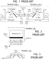
- One example is described in Hsu-Liang Hsiao et al., "Compact and passive- alignment 4-channel x 2.5-Gbps optical interconnect modules based on silicon optical benches with 45° micro-reflectors", OPTICS EXPRESS, 21 December 2009, Vol. 17, No. 26, pages 24250-24260 , illustrated in Figs. 1-3 .
- Fig. 1 shows optical fibers 104 (104.1 and 104.2) used to interconnect integrated circuits (chips) 110.1, 110.2 mounted on respective printed circuit boards (PCBs) 114.1, 114.2.
- Chip 110.1, fiber 104.1, and PCB 114.1 are part of a signal transmitting module 116.1.
- Chip 1101.2, fiber 104.2, and PCB 114.2 are part of a signal receiving module 116.2.
- Electrical signals from chip 110.1 are provided to an optoelectronic transducer 120.1 for conversion to light.
- Transducer 120.1 is an integrated circuit (IC or "chip") containing a semiconductor laser (vertical-cavity surface emitting laser, "VCSEL").
- Transducer 120.1 is mounted on a silicon interposer (silicon optical bench, or SiOB) 124.1 made using a silicon substrate 130.1.
- Conductive lines 134.1 transmit electrical signals from chip 110.1 to transducer 120.1.
- the transducer produces optical signals in a vertical light beam 140.1.
- Light beam 140.1 is reflected by a mirror 144.1 formed of a gold layer deposited on the silicon interposer's surface inclined at 45° to the horizontal. The reflected beam from mirror 144.1 enters the optical fiber 104.1.
- Fiber 104.1 is connected to a fiber 104.2 of module 116.2 by a connector 150.
- Module 116.2 is similar to module 116.1.
- the optical signals are emitted from fiber 104.2 in a horizontal beam 140.2, which is reflected by a 45° mirror 144.2 to travel vertically to a transducer 120.2.
- the mirror is part of a silicon interposer 124.2 made using silicon substrate 130.2.
- Transducer 120.2 is mounted on interposer 124.2.
- Transducer 120.2 is a photodetector integrated circuit which converts the optical signals into electric signals provided, via conductive lines 134.2, to chip 110.2.
- Interposer 124.2 and chip 110.2 are mounted on PCB 114.2.
- Figs. 2 and 3 illustrate a module 116 which can be 116.1 or 116.2.
- Fig. 2 is a top view, and Fig. 3 shows a cross section by a plane transversal to fibers 104.
- Each module 116.1, 116.2 has four fibers 104 (i.e. 104.1 or 104.2);
- transducer 120.1 has four lasers emitting four respective beams 140.1 entering four respective fibers 104.1;
- transducer 120.2 has four photodetectors which receive four respective beams 140.2 passing through four respective fibers 104.2.
- monocrystalline silicon substrate 130 having (100)-orientation supports all the four fibers 104.
- the fibers are mounted in V-grooves 310 formed by a wet etch of substrate 130.
- the etch also forms the silicon surface underlying the mirror 144.
- the V-grooves have 45°-sloped sidewalls.
- the 45° angle is produced by an anisotropic wet etch of silicon substrate 130 which is a monocrystalline silicon wafer of (100)-orientation.
- the sloped sidewalls are (110) crystal planes.
- the etchant is a solution of KOH (potassium hydroxide) and isopropyl alcohol (IPA) chosen to suppress the etching rate of ⁇ 110 ⁇ planes to a level below the etching rate of ⁇ 111 ⁇ planes.
- the 45° angle so produced is highly precise, which helps in precise positioning of fibers 104 because the fibers do not reach the groove bottom and the fiber position is therefore determined by the angle of the grooves' sidewalls (45°) and the groove's width at the top.
- the document EP 0 827 211 A2 describes an integrated photonics device.
- the integrated photonics device includes a photo detector having an active area.
- a substrate has a side surface intersecting a top surface of the substrate at a predetermined angle.
- the side surface is reflective.
- the photo detector is bonded onto the top surface of the substrate with the active area of the photo detector facing the side surface such that light traveling parallel to the top surface of the substrate can be reflected onto the active area of the photo detector via the side surface.
- the document US 2003/034438 A1 discloses a connector for optically connecting an optoelectronic device (e.g. VCSELS or photodetectors) and an array of optical waveguides (e.g. optical fibers or integrated optical waveguides).
- the device has a submount chip for holding the optoelectronic device.
- the submount chip has a micromachined pit and the OE device is disposed in the pit.
- the pit has sidewalls that provide mechanical alignment for the OE device.
- the submount also has holes for receiving guide pins.
- the connector also has a waveguide array such as a V-groove optical fiber array.
- the waveguide array has edges of holes for contact with the guide pins. When the guide pins are inserted into the submount chip, the waveguides are automatically aligned with the optical waveguides.
- EP0535690 discloses a light receiving module comprising a semiconductor substrate, a light receiving element mounted on a surface of the semiconductor substrate, a groove formed on a back surface of the semiconductor substrate, an inclined face at a distal end of the optical fiber, the inclined face facing the light receiving element, and an optical fiber fixed in the groove. A light signal transmitted through the fiber is reflected by the inclined face. The reflected light is admitted to a light receiving face of the light receiving element, from the back surface side of the semiconductor substrate.
- US2007/281493 discloses a single crystal silicon etching method including providing a single crystal silicon substrate having at least one trench therein. The substrate is exposed to an anisotropic etchant which undercuts the silicon. By controlling the length of the etch, single crystal silicon islands or smooth vertical walls in the single crystal silicon may be created.
- employed mirrors can be, for example, just silicon surfaces or other non-metal surfaces.
- the mirrors employed in the embodiments of the structure according to the present invention are at a retrograde angle, i.e. an angle greater than 90°.
- a 135° angle can be used in a wide variety of MEMS (micro-electromechanical systems).
- substrate 130 has a cavity 410 with sidewalls at 135° to the horizontal plane.
- the bottom planar surface of cavity 410 can be a sensor's membrane.
- the fabrication process of forming the cavity 410 can replace the sensor fabrication process which uses two fusion-bonded wafers and which is described in " The MEMS Handbook" (edited by Mohamed Gad-el-Hak, CRC Press 2001), chapter 16 ("MEMS Fabrication”), section 16.8.2.3 .
- the silicon interposer of Fig. 4 can be manufactured using a monocrystalline silicon substrate 130 having (100) orientation.
- a suitable mask 810 e.g. thermal or CVD silicon dioxide
- the mask opening is rectangular, with sides 5210.1-5210.4 extending along ⁇ 100> directions.
- a retrograde angle of 135° will be formed at one or more or these sides as described below.
- each side at which the retrograde angle is desired extends along a ⁇ 100> direction, but the other sides may extend along different directions.
- the invention is not limited to rectangular mask openings.
- An anisotropic, perfectly vertical etch selective to mask 810 forms a cavity 410 ( Fig. 6 , vertical cross section) with vertical sidewalls.
- This can be a dry etch for example.
- a wet etch is conducted selective to the ⁇ 110 ⁇ silicon planes to deepen the cavity and undercut the cavity edges to form retrograde, 135° sidewalls.
- the cavity depth is doubled or more than doubled by the wet etch.
- Spacers and the grooves can be defined by mask 810 ( Figs. 5A-5B ), i.e. the mask 810 can cover the spacer areas between the grooves.
- the spacers and the grooves will then be formed by the etches of Figs. 6, 7 .
- the grooves have retrograde sidewalls - a groove's transversal cross section can be as in Fig. 5 .
- the retrograde sidewalls can be at an angle other than 135°. For example, a 125.3° angle is possible if the sidewalls are ⁇ 111 ⁇ planes in a (100) or (110) wafer. To get such angle, side 5210.2 should be oriented [111] in a (100) wafer, and should be oriented [100] in a (110) wafer.
- fibers 104 are optional; the light beams are transmitted through space without fibers.
- the light beams are laser beams.
- the retrograde sidewalls are used for MEMS applications as mentioned above in connection with Fig. 4 .
- Fig. 8 vertical cross section as in Fig. 7 shows a sensor based on a silicon structure such as shown in Fig. 4 or 7 .
- the sensor is made of a monocrystalline silicon wafer 130 having a (100) orientation and having a cavity 410 with at least two retrograde sidewalls at 135° or 125.3° angles formed by silicon crystal planes.
- the cavity can be formed as described above in connection with Figs. 5A-7 .
- Thin substrate portion 6010 at the cavity bottom provides a membrane whose deformations are detected by circuitry 6020 shown as a number of blocks formed at the top and/or bottom surfaces of substrate 130.
- Circuit blocks 6020 may include elements integrated with the substrate 130 and/or external elements connected to the substrate.
- the membrane motion can be optically detected as illustrated in Fig. 9 .
- the cavity sidewalls 5210.2, 5210.4 are at 135° as in Fig. 7 .
- Transmitter 120.1 and receiver 120.2 (which may be transducers formed in separate semiconductor chips or in the same chip) can be rigidly attached to the bottom of membrane 6010 so that they move with the membrane when the membrane deforms, or they can be mounted on a separate mount (not shown) so as not to change their position when the membrane deforms.
- Transmitter 120.1 transmits a light beam 140 (e.g. laser beam) through the membrane. If membrane 6010 is horizontal, then the beam is reflected by cavity sidewall 5210.2 to travel horizontally to sidewall 5210.4.
- a light beam 140 e.g. laser beam
- Sidewall 5210.4 reflects the beam to travel vertically downward through membrane 6010 to receiver 120.2. If the membrane is deformed, then the path of beam 140 will change, and the beam will not hit the receiver 120.2 or will hit the receiver in a different manner, with different measurable parameters, e.g. at a different portion of receiver 120.2 and/or at a different angle and or at a different spatial distribution of the intensity and/or with a different phase and/or polarization. These differences are detected by receiver 120.2 to provide sensing signals (e.g. electrical signals indicative of the differences).
- sensing signals e.g. electrical signals indicative of the differences.
- the sensors of Figs. 8, 9 can be used to detect and measure the membrane displacement and/or vibration and/or strain (i.e. pressure on the membrane). Other parameters can also be measured if they are affected by the membrane's displacement or deformation or vibration. Such parameters include temperature, electrical conductivity, electrical resistance, strain, pressure, reflectivity, refractive index, and possibly other parameters.
- sidewalls 5210 of structures of Fig. 7 can be used as reflective surfaces for interchip communications.
- the reflective properties of a retrograde sidewall employed in a structure according to the present invention can be improved by forming a smooth reflective layer which provides desired reflection properties, e.g. desired smoothness and desired reflectivity in a desired wavelength range.
- a smooth reflective layer which provides desired reflection properties, e.g. desired smoothness and desired reflectivity in a desired wavelength range.
- aluminum or copper can be deposited by chemical vapor deposition (CVD).
- Sputtering can also be used, followed by re-sputtering.
- a layer of a suitable reflective material e.g. metal (possibly aluminum, copper, gold, silver, or other suitable materials or their combinations) can be sputter-deposited on the top surface of substrate 130.
- Layer is non-conformal, covering the surfaces in the line of sight of the sputtering target (not shown) but not covering the retrograde sidewalls. Then re-sputtering is performed. In this process, the layer is bombarded by ions or atoms (e.g. argon) which dislodge the atoms of layer. Some of the atoms dislodged from the bottom of cavity 410 deposit on mirror sidewall 5210.2 and possibly other retrograde sidewalls to provide the reflective mirror 144.
- ions or atoms e.g. argon
- mirrors can be formed on a separate substrate (not shown), then released from the separate substrate and glued to the mirror sidewall or sidewalls (e.g. 5210.2) with an adhesive.
- waveguides other than optical fibers can be provided, for any suitable wavelengths including, but not limited to, visible light (from about 380 tun to about 740 nm), or infrared radiation (from about 10 nm and up to the visible light), or ultraviolet radiation (from about the visible light and up to about 300 um. Other variations are also possible.
- Some embodiments provide a substrate comprising a region of monocrystalline silicon (e.g. region 130 in Fig. 7 ), the region comprising:
- a second surface which is a crystal plane (e.g. ⁇ 110 ⁇ plane) of the monocrystalline silicon (this could be a sidewall surface 5210.2 of cavity 410);
- first and second surfaces meet at an angle of 135° or 125.3° to each other, the angle being measured through a space occupied by the monocrystalline silicon (e.g. angle ⁇ in Fig. 4 ).
- the embodiments comprise a transducer meeting the second segment of the path, for receiving the electromagnetic waves from the path or for transmitting the electromagnetic waves into the path.
- the transducer is attached to the substrate.
- the electromagnetic waves are in the wavelength range of 10 nm to 300 micrometers.
- Some embodiments provide a method for manufacturing a substrate, the method comprising:
- a region of monocrystalline silicon the region having a first surface (e.g. top surface of substrate 130 in Fig. 5A ) which is a crystal plane (e.g. (100) plane) of the monocrystalline silicon;
- the via in the first surface (e.g. the via can be cavity 410 in Fig. 6 , or can be a through hole), the via having a sidewall which forms an angle or angles less than a predefined angle ⁇ of 135° or 125.3°, the angle a being the angle between the sidewall and a first plane passing through the via's bottom and parallel to the first surface (e.g. the first plane can be the bottom surface of cavity 410 in Fig. 6 ; if the via is a through hole, the first plane can be a horizontal plane passing through the via bottom), the angle a being measured through the monocrystalline silicon region; and
Landscapes
- Physics & Mathematics (AREA)
- General Physics & Mathematics (AREA)
- Optics & Photonics (AREA)
- Optical Couplings Of Light Guides (AREA)
- Micromachines (AREA)
- Weting (AREA)
- Optical Integrated Circuits (AREA)
Applications Claiming Priority (4)
| Application Number | Priority Date | Filing Date | Title |
|---|---|---|---|
| US201261585217P | 2012-01-10 | 2012-01-10 | |
| US13/362,898 US8757897B2 (en) | 2012-01-10 | 2012-01-31 | Optical interposer |
| US13/454,713 US9323010B2 (en) | 2012-01-10 | 2012-04-24 | Structures formed using monocrystalline silicon and/or other materials for optical and other applications |
| PCT/US2013/020562 WO2013106285A2 (en) | 2012-01-10 | 2013-01-07 | Structures formed using monocrystalline silicon and/or other materials for optical and other applications |
Publications (2)
| Publication Number | Publication Date |
|---|---|
| EP2802916A2 EP2802916A2 (en) | 2014-11-19 |
| EP2802916B1 true EP2802916B1 (en) | 2020-03-11 |
Family
ID=48743988
Family Applications (2)
| Application Number | Title | Priority Date | Filing Date |
|---|---|---|---|
| EP13702514.4A Active EP2802916B1 (en) | 2012-01-10 | 2013-01-07 | Structures formed using monocrystalline silicon and/or other materials for optical and other applications |
| EP13700811.6A Active EP2802915B1 (en) | 2012-01-10 | 2013-01-07 | Optical interposer |
Family Applications After (1)
| Application Number | Title | Priority Date | Filing Date |
|---|---|---|---|
| EP13700811.6A Active EP2802915B1 (en) | 2012-01-10 | 2013-01-07 | Optical interposer |
Country Status (7)
| Country | Link |
|---|---|
| US (1) | US9323010B2 (https=) |
| EP (2) | EP2802916B1 (https=) |
| JP (1) | JP5970081B2 (https=) |
| KR (2) | KR101955060B1 (https=) |
| CN (2) | CN104364688B (https=) |
| TW (2) | TWI553368B (https=) |
| WO (2) | WO2013106288A1 (https=) |
Families Citing this family (38)
| Publication number | Priority date | Publication date | Assignee | Title |
|---|---|---|---|---|
| US8508028B2 (en) * | 2010-07-16 | 2013-08-13 | Yu-Lung Huang | Chip package and method for forming the same |
| TW201417250A (zh) * | 2012-07-17 | 2014-05-01 | 海特根微光學公司 | 光學模組,特別是光電模組,及其製造方法 |
| US9529162B2 (en) * | 2012-10-09 | 2016-12-27 | Corning Optical Communications LLC | Optical fiber connectors and methods of forming optical fiber connectors |
| US9484211B2 (en) | 2013-01-24 | 2016-11-01 | Taiwan Semiconductor Manufacturing Company, Ltd. | Etchant and etching process |
| DE102013224607B4 (de) | 2013-11-29 | 2024-06-06 | Robert Bosch Gmbh | Mikro-elektromechanische Anordnung und Verfahren zum Aufbau einer mikro-elektromechanischen Anordnung |
| JP6382313B2 (ja) * | 2013-12-20 | 2018-08-29 | インテル コーポレイション | テーパー状導波路構造を有する光検出器 |
| CN104752192B (zh) * | 2013-12-31 | 2017-11-14 | 中芯国际集成电路制造(上海)有限公司 | 一种在半导体衬底表面制作斜面的方法 |
| US9395491B2 (en) * | 2014-02-05 | 2016-07-19 | Aurrion, Inc. | Shielding regions for photonic integrated circuits |
| CN103955129A (zh) * | 2014-04-10 | 2014-07-30 | 中国电子科技集团公司第三十八研究所 | 具有双反射镜的微型原子气体腔器件及其制造方法 |
| CN103941576A (zh) * | 2014-04-10 | 2014-07-23 | 中国电子科技集团公司第三十八研究所 | 基于mems技术的原子气体腔器件及其制造方法 |
| CN103941577A (zh) * | 2014-04-10 | 2014-07-23 | 中国电子科技集团公司第三十八研究所 | 具有双反射镜和凹槽形结构的原子气体腔器件及其制造方法 |
| TWI549259B (zh) * | 2014-05-15 | 2016-09-11 | 國立清華大學 | 全集成主被動積體光學於矽基積體電路及其製作方法 |
| US9274277B2 (en) | 2014-05-15 | 2016-03-01 | Globalfoundries Inc. | Waveguide devices with supporting anchors |
| CN104465855B (zh) * | 2014-11-24 | 2017-02-22 | 华天科技(昆山)电子有限公司 | 晶圆级光互连模块及制作方法 |
| US9498120B2 (en) | 2014-12-22 | 2016-11-22 | Carl Zeiss Meditec Ag | Method and system for optical coherence elastography of posterior parts of the eye |
| CN104966670A (zh) * | 2015-06-25 | 2015-10-07 | 中国工程物理研究院电子工程研究所 | 一种单晶硅刻蚀方法及刻蚀液 |
| JP6217706B2 (ja) | 2015-07-29 | 2017-10-25 | 日亜化学工業株式会社 | 光学部材の製造方法、半導体レーザ装置の製造方法及び半導体レーザ装置 |
| JP6354704B2 (ja) * | 2015-08-25 | 2018-07-11 | 日亜化学工業株式会社 | 光学部材の製造方法、半導体レーザ装置の製造方法及び半導体レーザ装置 |
| CN105321929B (zh) * | 2015-08-26 | 2018-05-08 | 中国科学院微电子研究所 | 一种三维光电集成结构及其制作方法 |
| CN105336795B (zh) * | 2015-08-26 | 2017-03-22 | 中国科学院微电子研究所 | 一种基于光栅接口的光子芯片封装结构及其制作方法 |
| WO2017036827A1 (en) * | 2015-09-03 | 2017-03-09 | Koninklijke Philips N.V. | Ic die, probe and ultrasound system |
| US10408926B2 (en) | 2015-09-18 | 2019-09-10 | Qualcomm Incorporated | Implementation of the focal plane 2D APD array for hyperion lidar system |
| US9910232B2 (en) * | 2015-10-21 | 2018-03-06 | Luxtera, Inc. | Method and system for a chip-on-wafer-on-substrate assembly |
| US10705293B2 (en) * | 2015-12-14 | 2020-07-07 | Intel Corporation | Substrate integrated waveguide |
| US10209477B1 (en) * | 2017-05-25 | 2019-02-19 | Lockheed Martin Coherent Technologies, Inc. | Systems and methods for reconfigurable micro-optic assemblies |
| US10168495B1 (en) * | 2017-06-28 | 2019-01-01 | Kyocera Corporation | Optical waveguide and optical circuit board |
| JP6631609B2 (ja) * | 2017-09-26 | 2020-01-15 | 日亜化学工業株式会社 | 半導体レーザ装置の製造方法 |
| US20190237629A1 (en) | 2018-01-26 | 2019-08-01 | Lumileds Llc | Optically transparent adhesion layer to connect noble metals to oxides |
| US10930628B2 (en) * | 2018-06-27 | 2021-02-23 | Taiwan Semiconductor Manufacturing Company, Ltd. | Photonic semiconductor device and method |
| US11327348B2 (en) * | 2018-09-18 | 2022-05-10 | Eagle Technology, Llc | Multi-channel laser system including optical assembly with etched optical signal channels and related methods |
| US11042052B2 (en) | 2018-09-18 | 2021-06-22 | Eagle Technology, Llc | Multi-channel laser system including an acousto-optic modulator (AOM) with beam polarization switching and related methods |
| CN111951693B (zh) * | 2019-05-17 | 2022-11-15 | 浙江宇视科技有限公司 | 一种阵列器件的定位方法、装置、存储介质及电子设备 |
| US11887985B2 (en) | 2021-03-04 | 2024-01-30 | Taiwan Semiconductor Manufacturing Co., Ltd. | Semiconductor device and method |
| US11940659B2 (en) | 2021-08-30 | 2024-03-26 | Taiwan Semiconductor Manufacturing Company Limited | Optical integrated circuit structure including edge coupling protective features and methods of forming same |
| US11774689B2 (en) | 2021-10-25 | 2023-10-03 | Globalfoundries U.S. Inc. | Photonics chips and semiconductor products having angled optical fibers |
| TWI831270B (zh) * | 2022-04-01 | 2024-02-01 | 欣興電子股份有限公司 | 電子裝置 |
| CN115508956B (zh) * | 2022-09-22 | 2024-04-16 | 希烽光电科技(南京)有限公司 | 倾斜基板高带宽光引擎 |
| US20250123553A1 (en) * | 2023-10-13 | 2025-04-17 | Taiwan Semiconductor Manufacturing Company Limited | System and method for patterned layer design and formation |
Citations (2)
| Publication number | Priority date | Publication date | Assignee | Title |
|---|---|---|---|---|
| EP0535690A1 (en) * | 1991-10-02 | 1993-04-07 | Sumitomo Electric Industries, Limited | Light receiving module |
| US20070281493A1 (en) * | 2006-06-02 | 2007-12-06 | Janos Fucsko | Methods of shaping vertical single crystal silicon walls and resulting structures |
Family Cites Families (64)
| Publication number | Priority date | Publication date | Assignee | Title |
|---|---|---|---|---|
| US3761782A (en) | 1971-05-19 | 1973-09-25 | Signetics Corp | Semiconductor structure, assembly and method |
| EP0311695B1 (en) | 1987-04-24 | 1994-11-30 | Enplas Laboratories, Inc. | Force and moment detector using resistor |
| US5229647A (en) | 1991-03-27 | 1993-07-20 | Micron Technology, Inc. | High density data storage using stacked wafers |
| US5502314A (en) * | 1993-07-05 | 1996-03-26 | Matsushita Electric Industrial Co., Ltd. | Field-emission element having a cathode with a small radius |
| US5359687A (en) * | 1993-08-23 | 1994-10-25 | Alliedsignal Inc. | Polymer microstructures which facilitate fiber optic to waveguide coupling |
| WO1996022177A1 (de) | 1995-01-18 | 1996-07-25 | Robert Bosch Gmbh | Anordnung zur umsetzung von optischen in elektrische signale und verfahren zur herstellung |
| KR100441810B1 (ko) * | 1995-09-29 | 2004-10-20 | 모토로라 인코포레이티드 | 광전달구조물을정렬하기위한전자장치 |
| JPH09320996A (ja) | 1996-03-29 | 1997-12-12 | Denso Corp | 半導体装置の製造方法 |
| US5808293A (en) * | 1996-08-28 | 1998-09-15 | Hewlett-Packard Company | Photo detector with an integrated mirror and a method of making the same |
| US6332719B1 (en) | 1997-06-25 | 2001-12-25 | Matsushita Electric Industrial Co., Ltd. | Optical transmitter/receiver apparatus, method for fabricating the same and optical semiconductor module |
| JP4019538B2 (ja) * | 1998-03-16 | 2007-12-12 | 住友電気工業株式会社 | 光モジュール用基体及び光モジュール |
| US6115521A (en) * | 1998-05-07 | 2000-09-05 | Trw Inc. | Fiber/waveguide-mirror-lens alignment device |
| DK0987769T3 (da) | 1998-09-18 | 2003-07-14 | Sumitomo Electric Industries | Fotodiodemodul |
| US6246026B1 (en) | 1998-09-18 | 2001-06-12 | The Whitaker Corporation | Process for cutting an optical fiber |
| US20030034438A1 (en) | 1998-11-25 | 2003-02-20 | Sherrer David W. | Optoelectronic device-optical fiber connector having micromachined pit for passive alignment of the optoelectronic device |
| US6625357B2 (en) | 1999-03-29 | 2003-09-23 | Tyco Electronics Corporation | Method for fabricating fiducials for passive alignment of opto-electronic devices |
| JP2001021775A (ja) * | 1999-07-09 | 2001-01-26 | Sumitomo Electric Ind Ltd | 光学装置 |
| US6266472B1 (en) * | 1999-09-03 | 2001-07-24 | Corning Incorporated | Polymer gripping elements for optical fiber splicing |
| US20010053260A1 (en) * | 2000-03-13 | 2001-12-20 | Toshiyuki Takizawa | Optical module and method for producing the same, and optical circuit device |
| US6737223B2 (en) | 2000-08-07 | 2004-05-18 | Shipley Company, L.L.C. | Fiber optic chip with lenslet array and method of fabrication |
| JP3921940B2 (ja) * | 2000-12-07 | 2007-05-30 | 住友電気工業株式会社 | 光送受信モジュール |
| US6863209B2 (en) * | 2000-12-15 | 2005-03-08 | Unitivie International Limited | Low temperature methods of bonding components |
| US6439703B1 (en) | 2000-12-29 | 2002-08-27 | Eastman Kodak Company | CMOS/MEMS integrated ink jet print head with silicon based lateral flow nozzle architecture and method of forming same |
| US6498381B2 (en) | 2001-02-22 | 2002-12-24 | Tru-Si Technologies, Inc. | Semiconductor structures having multiple conductive layers in an opening, and methods for fabricating same |
| US6717254B2 (en) | 2001-02-22 | 2004-04-06 | Tru-Si Technologies, Inc. | Devices having substrates with opening passing through the substrates and conductors in the openings, and methods of manufacture |
| US6787916B2 (en) | 2001-09-13 | 2004-09-07 | Tru-Si Technologies, Inc. | Structures having a substrate with a cavity and having an integrated circuit bonded to a contact pad located in the cavity |
| JP2003167175A (ja) | 2001-12-04 | 2003-06-13 | Matsushita Electric Ind Co Ltd | 光実装基板及び光デバイス |
| JP2003177272A (ja) * | 2001-12-12 | 2003-06-27 | Alps Electric Co Ltd | 光合分波器とその製造方法及び光合分波モジュール |
| JP3750649B2 (ja) | 2001-12-25 | 2006-03-01 | 住友電気工業株式会社 | 光通信装置 |
| US6928226B2 (en) * | 2002-03-14 | 2005-08-09 | Corning Incorporated | Fiber and lens grippers, optical devices and methods of manufacture |
| WO2003088286A2 (en) | 2002-04-16 | 2003-10-23 | Xloom Photonics Ltd. | Electro-optical circuitry having integrated connector and methods for the production thereof |
| US6730540B2 (en) | 2002-04-18 | 2004-05-04 | Tru-Si Technologies, Inc. | Clock distribution networks and conductive lines in semiconductor integrated circuits |
| JPWO2003096095A1 (ja) * | 2002-05-09 | 2005-09-15 | 住友電気工業株式会社 | 光デバイス |
| KR20040081838A (ko) * | 2003-03-17 | 2004-09-23 | 엘지전자 주식회사 | 양면형 및 다층형 광 백플레인 기판 및 그 제조방법 |
| US6897148B2 (en) | 2003-04-09 | 2005-05-24 | Tru-Si Technologies, Inc. | Electroplating and electroless plating of conductive materials into openings, and structures obtained thereby |
| TWI254025B (en) | 2003-05-23 | 2006-05-01 | Rohm & Haas Elect Mat | Etching process for micromachining crystalline materials and devices fabricated thereby |
| US6985645B2 (en) * | 2003-09-24 | 2006-01-10 | International Business Machines Corporation | Apparatus and methods for integrally packaging optoelectronic devices, IC chips and optical transmission lines |
| US7060601B2 (en) | 2003-12-17 | 2006-06-13 | Tru-Si Technologies, Inc. | Packaging substrates for integrated circuits and soldering methods |
| US7049170B2 (en) | 2003-12-17 | 2006-05-23 | Tru-Si Technologies, Inc. | Integrated circuits and packaging substrates with cavities, and attachment methods including insertion of protruding contact pads into cavities |
| KR20050076742A (ko) | 2004-01-22 | 2005-07-27 | 마츠시타 덴끼 산교 가부시키가이샤 | 광전송로 기판의 제조방법, 광전송로 기판, 광전송로내장기판, 광전송로 내장기판의 제조방법 및 데이터처리장치 |
| US7713053B2 (en) | 2005-06-10 | 2010-05-11 | Protochips, Inc. | Reusable template for creation of thin films; method of making and using template; and thin films produced from template |
| US7547637B2 (en) * | 2005-06-21 | 2009-06-16 | Intel Corporation | Methods for patterning a semiconductor film |
| TW200714949A (en) | 2005-08-15 | 2007-04-16 | Rohm & Haas Elect Mat | Bonding methods and optical assemblies |
| US20070189659A1 (en) | 2006-01-29 | 2007-08-16 | Jeng-Jye Shau | Thin Film Optical Patterning Devices |
| JP2007298770A (ja) * | 2006-04-28 | 2007-11-15 | Nec Corp | 光導波路デバイス及びその製造方法 |
| US7510928B2 (en) | 2006-05-05 | 2009-03-31 | Tru-Si Technologies, Inc. | Dielectric trenches, nickel/tantalum oxide structures, and chemical mechanical polishing techniques |
| US7628932B2 (en) * | 2006-06-02 | 2009-12-08 | Micron Technology, Inc. | Wet etch suitable for creating square cuts in si |
| DE102006034236B3 (de) * | 2006-07-25 | 2008-05-15 | Airbus Deutschland Gmbh | Halterung für Lichtwellenleiter |
| US8304805B2 (en) * | 2009-01-09 | 2012-11-06 | Taiwan Semiconductor Manufacturing Company, Ltd. | Semiconductor diodes fabricated by aspect ratio trapping with coalesced films |
| US7485965B2 (en) * | 2007-05-25 | 2009-02-03 | International Business Machines Corporation | Through via in ultra high resistivity wafer and related methods |
| JP4577376B2 (ja) | 2008-02-21 | 2010-11-10 | ソニー株式会社 | 光導波路の製造方法 |
| TWI402549B (zh) * | 2008-04-09 | 2013-07-21 | Ind Tech Res Inst | 光電互連模組 |
| EP2216670B1 (en) | 2009-02-10 | 2016-06-22 | Tyco Electronics Raychem BVBA | Insert for an optical fiber assembly and optical fiber assembly using such an insert |
| US20120099820A1 (en) | 2009-03-20 | 2012-04-26 | Rolston David R | Two dimensional optical connector |
| JP5465453B2 (ja) * | 2009-03-26 | 2014-04-09 | パナソニック株式会社 | 光導波路形成用エポキシ樹脂組成物、光導波路形成用硬化性フィルム、光伝送用フレキシブルプリント配線板、及び電子情報機器 |
| CN101852898B (zh) | 2009-03-30 | 2014-03-12 | 日立电线株式会社 | 光连接器及使用了光连接器的光纤模块 |
| US8031993B2 (en) | 2009-07-28 | 2011-10-04 | Tyco Electronics Corporation | Optical fiber interconnect device |
| US8611716B2 (en) | 2009-09-30 | 2013-12-17 | Corning Incorporated | Channeled substrates for integrated optical devices employing optical fibers |
| US8791405B2 (en) * | 2009-12-03 | 2014-07-29 | Samsung Electronics Co., Ltd. | Optical waveguide and coupler apparatus and method of manufacturing the same |
| US7949211B1 (en) | 2010-02-26 | 2011-05-24 | Corning Incorporated | Modular active board subassemblies and printed wiring boards comprising the same |
| TWI446036B (zh) * | 2010-05-24 | 2014-07-21 | Univ Nat Central | 光學傳輸模組 |
| TWI414478B (zh) | 2010-09-09 | 2013-11-11 | Domintech Co Ltd | 可同時量測加速度及壓力之微機電感測器 |
| US20120146101A1 (en) * | 2010-12-13 | 2012-06-14 | Chun-Hsien Lin | Multi-gate transistor devices and manufacturing method thereof |
| US8757897B2 (en) * | 2012-01-10 | 2014-06-24 | Invensas Corporation | Optical interposer |
-
2012
- 2012-04-24 US US13/454,713 patent/US9323010B2/en active Active
- 2012-12-28 TW TW101150997A patent/TWI553368B/zh not_active IP Right Cessation
- 2012-12-28 TW TW101150996A patent/TWI539191B/zh not_active IP Right Cessation
-
2013
- 2013-01-07 WO PCT/US2013/020578 patent/WO2013106288A1/en not_active Ceased
- 2013-01-07 CN CN201380013246.6A patent/CN104364688B/zh active Active
- 2013-01-07 EP EP13702514.4A patent/EP2802916B1/en active Active
- 2013-01-07 KR KR1020147022313A patent/KR101955060B1/ko active Active
- 2013-01-07 EP EP13700811.6A patent/EP2802915B1/en active Active
- 2013-01-07 CN CN201380013259.3A patent/CN104169768B/zh active Active
- 2013-01-07 WO PCT/US2013/020562 patent/WO2013106285A2/en not_active Ceased
- 2013-01-07 JP JP2014552231A patent/JP5970081B2/ja active Active
- 2013-01-07 KR KR1020147022311A patent/KR101870490B1/ko active Active
Patent Citations (2)
| Publication number | Priority date | Publication date | Assignee | Title |
|---|---|---|---|---|
| EP0535690A1 (en) * | 1991-10-02 | 1993-04-07 | Sumitomo Electric Industries, Limited | Light receiving module |
| US20070281493A1 (en) * | 2006-06-02 | 2007-12-06 | Janos Fucsko | Methods of shaping vertical single crystal silicon walls and resulting structures |
Also Published As
| Publication number | Publication date |
|---|---|
| KR101955060B1 (ko) | 2019-03-06 |
| US20130177274A1 (en) | 2013-07-11 |
| TWI539191B (zh) | 2016-06-21 |
| US9323010B2 (en) | 2016-04-26 |
| WO2013106285A3 (en) | 2013-09-26 |
| JP5970081B2 (ja) | 2016-08-17 |
| TW201333562A (zh) | 2013-08-16 |
| EP2802915B1 (en) | 2017-04-12 |
| EP2802916A2 (en) | 2014-11-19 |
| CN104169768B (zh) | 2016-03-02 |
| CN104364688A (zh) | 2015-02-18 |
| TWI553368B (zh) | 2016-10-11 |
| JP2015515113A (ja) | 2015-05-21 |
| WO2013106285A2 (en) | 2013-07-18 |
| KR101870490B1 (ko) | 2018-06-22 |
| CN104169768A (zh) | 2014-11-26 |
| EP2802915A1 (en) | 2014-11-19 |
| KR20140112069A (ko) | 2014-09-22 |
| KR20140112068A (ko) | 2014-09-22 |
| TW201333567A (zh) | 2013-08-16 |
| CN104364688B (zh) | 2016-08-24 |
| WO2013106288A1 (en) | 2013-07-18 |
Similar Documents
| Publication | Publication Date | Title |
|---|---|---|
| EP2802916B1 (en) | Structures formed using monocrystalline silicon and/or other materials for optical and other applications | |
| US8548284B2 (en) | Optical element module and method of manufacturing the same | |
| US7355720B1 (en) | Optical displacement sensor | |
| EP2460042B1 (en) | Optical fiber interconnect device | |
| WO2018213039A1 (en) | Polymer-based 1x2 vertical optical splitters on silicon substrate | |
| US20110129181A1 (en) | Turning mirror for photonic integrated circuits | |
| TW442678B (en) | Connector-type optical transceiver using SOI optical waveguide | |
| US8818145B2 (en) | Optical interposer with transparent substrate | |
| KR101467166B1 (ko) | 미러링된 기판을 사용한 광 수신기 아키텍처 | |
| US8090266B2 (en) | Optically coupling components of a transceiver | |
| KR19980045943A (ko) | 하이브리드 광집적회로용 마이크로 거울, 그의 제조방법, 마이크로 거울-광검출기 어셈블리 및 광수신용 하이브리드 광집적회로 어셈블리 | |
| US9651749B1 (en) | Interposer with opaque substrate | |
| KR101416638B1 (ko) | 평면 광도파로의 광신호 모니터링 장치 | |
| KR100439760B1 (ko) | 광연결봉을 이용한 광연결 장치 | |
| Nieweglowski et al. | Optical analysis of short-distance optical interconnect on the PCB-level | |
| JP2009192816A (ja) | 双方向光送受信モジュール及びこれに用いる受光素子 | |
| JP3898448B2 (ja) | 光集積回路基板 | |
| Deimel | Micromachined devices for optical applications | |
| Koh et al. | Novel integrated optical I/O couplers on MCMs using MEMS techniques | |
| HK1181464A (en) | Optical receiver architecture using a mirrored substrate | |
| Kopp et al. | Compact parallel optical interface built with optical fiber tips |
Legal Events
| Date | Code | Title | Description |
|---|---|---|---|
| PUAI | Public reference made under article 153(3) epc to a published international application that has entered the european phase |
Free format text: ORIGINAL CODE: 0009012 |
|
| 17P | Request for examination filed |
Effective date: 20140808 |
|
| AK | Designated contracting states |
Kind code of ref document: A2 Designated state(s): AL AT BE BG CH CY CZ DE DK EE ES FI FR GB GR HR HU IE IS IT LI LT LU LV MC MK MT NL NO PL PT RO RS SE SI SK SM TR |
|
| DAX | Request for extension of the european patent (deleted) | ||
| STAA | Information on the status of an ep patent application or granted ep patent |
Free format text: STATUS: EXAMINATION IS IN PROGRESS |
|
| 17Q | First examination report despatched |
Effective date: 20170925 |
|
| GRAP | Despatch of communication of intention to grant a patent |
Free format text: ORIGINAL CODE: EPIDOSNIGR1 |
|
| STAA | Information on the status of an ep patent application or granted ep patent |
Free format text: STATUS: GRANT OF PATENT IS INTENDED |
|
| GRAS | Grant fee paid |
Free format text: ORIGINAL CODE: EPIDOSNIGR3 |
|
| INTG | Intention to grant announced |
Effective date: 20191127 |
|
| GRAA | (expected) grant |
Free format text: ORIGINAL CODE: 0009210 |
|
| STAA | Information on the status of an ep patent application or granted ep patent |
Free format text: STATUS: THE PATENT HAS BEEN GRANTED |
|
| AK | Designated contracting states |
Kind code of ref document: B1 Designated state(s): AL AT BE BG CH CY CZ DE DK EE ES FI FR GB GR HR HU IE IS IT LI LT LU LV MC MK MT NL NO PL PT RO RS SE SI SK SM TR |
|
| REG | Reference to a national code |
Ref country code: GB Ref legal event code: FG4D |
|
| REG | Reference to a national code |
Ref country code: CH Ref legal event code: EP |
|
| REG | Reference to a national code |
Ref country code: AT Ref legal event code: REF Ref document number: 1243875 Country of ref document: AT Kind code of ref document: T Effective date: 20200315 |
|
| REG | Reference to a national code |
Ref country code: IE Ref legal event code: FG4D |
|
| REG | Reference to a national code |
Ref country code: DE Ref legal event code: R096 Ref document number: 602013066642 Country of ref document: DE |
|
| PG25 | Lapsed in a contracting state [announced via postgrant information from national office to epo] |
Ref country code: RS Free format text: LAPSE BECAUSE OF FAILURE TO SUBMIT A TRANSLATION OF THE DESCRIPTION OR TO PAY THE FEE WITHIN THE PRESCRIBED TIME-LIMIT Effective date: 20200311 Ref country code: NO Free format text: LAPSE BECAUSE OF FAILURE TO SUBMIT A TRANSLATION OF THE DESCRIPTION OR TO PAY THE FEE WITHIN THE PRESCRIBED TIME-LIMIT Effective date: 20200611 Ref country code: FI Free format text: LAPSE BECAUSE OF FAILURE TO SUBMIT A TRANSLATION OF THE DESCRIPTION OR TO PAY THE FEE WITHIN THE PRESCRIBED TIME-LIMIT Effective date: 20200311 |
|
| REG | Reference to a national code |
Ref country code: NL Ref legal event code: MP Effective date: 20200311 |
|
| PG25 | Lapsed in a contracting state [announced via postgrant information from national office to epo] |
Ref country code: GR Free format text: LAPSE BECAUSE OF FAILURE TO SUBMIT A TRANSLATION OF THE DESCRIPTION OR TO PAY THE FEE WITHIN THE PRESCRIBED TIME-LIMIT Effective date: 20200612 Ref country code: BG Free format text: LAPSE BECAUSE OF FAILURE TO SUBMIT A TRANSLATION OF THE DESCRIPTION OR TO PAY THE FEE WITHIN THE PRESCRIBED TIME-LIMIT Effective date: 20200611 Ref country code: SE Free format text: LAPSE BECAUSE OF FAILURE TO SUBMIT A TRANSLATION OF THE DESCRIPTION OR TO PAY THE FEE WITHIN THE PRESCRIBED TIME-LIMIT Effective date: 20200311 Ref country code: LV Free format text: LAPSE BECAUSE OF FAILURE TO SUBMIT A TRANSLATION OF THE DESCRIPTION OR TO PAY THE FEE WITHIN THE PRESCRIBED TIME-LIMIT Effective date: 20200311 Ref country code: HR Free format text: LAPSE BECAUSE OF FAILURE TO SUBMIT A TRANSLATION OF THE DESCRIPTION OR TO PAY THE FEE WITHIN THE PRESCRIBED TIME-LIMIT Effective date: 20200311 |
|
| REG | Reference to a national code |
Ref country code: LT Ref legal event code: MG4D |
|
| PG25 | Lapsed in a contracting state [announced via postgrant information from national office to epo] |
Ref country code: NL Free format text: LAPSE BECAUSE OF FAILURE TO SUBMIT A TRANSLATION OF THE DESCRIPTION OR TO PAY THE FEE WITHIN THE PRESCRIBED TIME-LIMIT Effective date: 20200311 |
|
| PG25 | Lapsed in a contracting state [announced via postgrant information from national office to epo] |
Ref country code: CZ Free format text: LAPSE BECAUSE OF FAILURE TO SUBMIT A TRANSLATION OF THE DESCRIPTION OR TO PAY THE FEE WITHIN THE PRESCRIBED TIME-LIMIT Effective date: 20200311 Ref country code: RO Free format text: LAPSE BECAUSE OF FAILURE TO SUBMIT A TRANSLATION OF THE DESCRIPTION OR TO PAY THE FEE WITHIN THE PRESCRIBED TIME-LIMIT Effective date: 20200311 Ref country code: SM Free format text: LAPSE BECAUSE OF FAILURE TO SUBMIT A TRANSLATION OF THE DESCRIPTION OR TO PAY THE FEE WITHIN THE PRESCRIBED TIME-LIMIT Effective date: 20200311 Ref country code: EE Free format text: LAPSE BECAUSE OF FAILURE TO SUBMIT A TRANSLATION OF THE DESCRIPTION OR TO PAY THE FEE WITHIN THE PRESCRIBED TIME-LIMIT Effective date: 20200311 Ref country code: LT Free format text: LAPSE BECAUSE OF FAILURE TO SUBMIT A TRANSLATION OF THE DESCRIPTION OR TO PAY THE FEE WITHIN THE PRESCRIBED TIME-LIMIT Effective date: 20200311 Ref country code: IS Free format text: LAPSE BECAUSE OF FAILURE TO SUBMIT A TRANSLATION OF THE DESCRIPTION OR TO PAY THE FEE WITHIN THE PRESCRIBED TIME-LIMIT Effective date: 20200711 Ref country code: SK Free format text: LAPSE BECAUSE OF FAILURE TO SUBMIT A TRANSLATION OF THE DESCRIPTION OR TO PAY THE FEE WITHIN THE PRESCRIBED TIME-LIMIT Effective date: 20200311 Ref country code: PT Free format text: LAPSE BECAUSE OF FAILURE TO SUBMIT A TRANSLATION OF THE DESCRIPTION OR TO PAY THE FEE WITHIN THE PRESCRIBED TIME-LIMIT Effective date: 20200805 |
|
| REG | Reference to a national code |
Ref country code: AT Ref legal event code: MK05 Ref document number: 1243875 Country of ref document: AT Kind code of ref document: T Effective date: 20200311 |
|
| REG | Reference to a national code |
Ref country code: DE Ref legal event code: R097 Ref document number: 602013066642 Country of ref document: DE |
|
| PLBE | No opposition filed within time limit |
Free format text: ORIGINAL CODE: 0009261 |
|
| STAA | Information on the status of an ep patent application or granted ep patent |
Free format text: STATUS: NO OPPOSITION FILED WITHIN TIME LIMIT |
|
| PG25 | Lapsed in a contracting state [announced via postgrant information from national office to epo] |
Ref country code: ES Free format text: LAPSE BECAUSE OF FAILURE TO SUBMIT A TRANSLATION OF THE DESCRIPTION OR TO PAY THE FEE WITHIN THE PRESCRIBED TIME-LIMIT Effective date: 20200311 Ref country code: IT Free format text: LAPSE BECAUSE OF FAILURE TO SUBMIT A TRANSLATION OF THE DESCRIPTION OR TO PAY THE FEE WITHIN THE PRESCRIBED TIME-LIMIT Effective date: 20200311 Ref country code: AT Free format text: LAPSE BECAUSE OF FAILURE TO SUBMIT A TRANSLATION OF THE DESCRIPTION OR TO PAY THE FEE WITHIN THE PRESCRIBED TIME-LIMIT Effective date: 20200311 Ref country code: DK Free format text: LAPSE BECAUSE OF FAILURE TO SUBMIT A TRANSLATION OF THE DESCRIPTION OR TO PAY THE FEE WITHIN THE PRESCRIBED TIME-LIMIT Effective date: 20200311 |
|
| 26N | No opposition filed |
Effective date: 20201214 |
|
| PG25 | Lapsed in a contracting state [announced via postgrant information from national office to epo] |
Ref country code: PL Free format text: LAPSE BECAUSE OF FAILURE TO SUBMIT A TRANSLATION OF THE DESCRIPTION OR TO PAY THE FEE WITHIN THE PRESCRIBED TIME-LIMIT Effective date: 20200311 Ref country code: SI Free format text: LAPSE BECAUSE OF FAILURE TO SUBMIT A TRANSLATION OF THE DESCRIPTION OR TO PAY THE FEE WITHIN THE PRESCRIBED TIME-LIMIT Effective date: 20200311 |
|
| REG | Reference to a national code |
Ref country code: DE Ref legal event code: R119 Ref document number: 602013066642 Country of ref document: DE |
|
| PG25 | Lapsed in a contracting state [announced via postgrant information from national office to epo] |
Ref country code: MC Free format text: LAPSE BECAUSE OF FAILURE TO SUBMIT A TRANSLATION OF THE DESCRIPTION OR TO PAY THE FEE WITHIN THE PRESCRIBED TIME-LIMIT Effective date: 20200311 |
|
| REG | Reference to a national code |
Ref country code: CH Ref legal event code: PL |
|
| GBPC | Gb: european patent ceased through non-payment of renewal fee |
Effective date: 20210107 |
|
| PG25 | Lapsed in a contracting state [announced via postgrant information from national office to epo] |
Ref country code: LU Free format text: LAPSE BECAUSE OF NON-PAYMENT OF DUE FEES Effective date: 20210107 |
|
| REG | Reference to a national code |
Ref country code: BE Ref legal event code: MM Effective date: 20210131 |
|
| PG25 | Lapsed in a contracting state [announced via postgrant information from national office to epo] |
Ref country code: FR Free format text: LAPSE BECAUSE OF NON-PAYMENT OF DUE FEES Effective date: 20210131 |
|
| PG25 | Lapsed in a contracting state [announced via postgrant information from national office to epo] |
Ref country code: GB Free format text: LAPSE BECAUSE OF NON-PAYMENT OF DUE FEES Effective date: 20210107 Ref country code: DE Free format text: LAPSE BECAUSE OF NON-PAYMENT OF DUE FEES Effective date: 20210803 Ref country code: CH Free format text: LAPSE BECAUSE OF NON-PAYMENT OF DUE FEES Effective date: 20210131 Ref country code: LI Free format text: LAPSE BECAUSE OF NON-PAYMENT OF DUE FEES Effective date: 20210131 |
|
| PG25 | Lapsed in a contracting state [announced via postgrant information from national office to epo] |
Ref country code: IE Free format text: LAPSE BECAUSE OF NON-PAYMENT OF DUE FEES Effective date: 20210107 |
|
| PG25 | Lapsed in a contracting state [announced via postgrant information from national office to epo] |
Ref country code: BE Free format text: LAPSE BECAUSE OF NON-PAYMENT OF DUE FEES Effective date: 20210131 |
|
| PG25 | Lapsed in a contracting state [announced via postgrant information from national office to epo] |
Ref country code: HU Free format text: LAPSE BECAUSE OF FAILURE TO SUBMIT A TRANSLATION OF THE DESCRIPTION OR TO PAY THE FEE WITHIN THE PRESCRIBED TIME-LIMIT; INVALID AB INITIO Effective date: 20130107 |
|
| PG25 | Lapsed in a contracting state [announced via postgrant information from national office to epo] |
Ref country code: CY Free format text: LAPSE BECAUSE OF FAILURE TO SUBMIT A TRANSLATION OF THE DESCRIPTION OR TO PAY THE FEE WITHIN THE PRESCRIBED TIME-LIMIT Effective date: 20200311 |
|
| PG25 | Lapsed in a contracting state [announced via postgrant information from national office to epo] |
Ref country code: MK Free format text: LAPSE BECAUSE OF FAILURE TO SUBMIT A TRANSLATION OF THE DESCRIPTION OR TO PAY THE FEE WITHIN THE PRESCRIBED TIME-LIMIT Effective date: 20200311 |
|
| PG25 | Lapsed in a contracting state [announced via postgrant information from national office to epo] |
Ref country code: MT Free format text: LAPSE BECAUSE OF FAILURE TO SUBMIT A TRANSLATION OF THE DESCRIPTION OR TO PAY THE FEE WITHIN THE PRESCRIBED TIME-LIMIT Effective date: 20200311 |
|
| PG25 | Lapsed in a contracting state [announced via postgrant information from national office to epo] |
Ref country code: TR Free format text: LAPSE BECAUSE OF FAILURE TO SUBMIT A TRANSLATION OF THE DESCRIPTION OR TO PAY THE FEE WITHIN THE PRESCRIBED TIME-LIMIT Effective date: 20200311 |