EP2800159A1 - A magnetic tunnel junction element - Google Patents
A magnetic tunnel junction element Download PDFInfo
- Publication number
- EP2800159A1 EP2800159A1 EP20140172609 EP14172609A EP2800159A1 EP 2800159 A1 EP2800159 A1 EP 2800159A1 EP 20140172609 EP20140172609 EP 20140172609 EP 14172609 A EP14172609 A EP 14172609A EP 2800159 A1 EP2800159 A1 EP 2800159A1
- Authority
- EP
- European Patent Office
- Prior art keywords
- electrode
- mtj
- layer
- coupled
- mram
- Prior art date
- Legal status (The legal status is an assumption and is not a legal conclusion. Google has not performed a legal analysis and makes no representation as to the accuracy of the status listed.)
- Withdrawn
Links
Images

Classifications
-
- H—ELECTRICITY
- H10—SEMICONDUCTOR DEVICES; ELECTRIC SOLID-STATE DEVICES NOT OTHERWISE PROVIDED FOR
- H10N—ELECTRIC SOLID-STATE DEVICES NOT OTHERWISE PROVIDED FOR
- H10N50/00—Galvanomagnetic devices
- H10N50/10—Magnetoresistive devices
-
- G—PHYSICS
- G11—INFORMATION STORAGE
- G11C—STATIC STORES
- G11C11/00—Digital stores characterised by the use of particular electric or magnetic storage elements; Storage elements therefor
- G11C11/02—Digital stores characterised by the use of particular electric or magnetic storage elements; Storage elements therefor using magnetic elements
- G11C11/16—Digital stores characterised by the use of particular electric or magnetic storage elements; Storage elements therefor using magnetic elements using elements in which the storage effect is based on magnetic spin effect
- G11C11/161—Digital stores characterised by the use of particular electric or magnetic storage elements; Storage elements therefor using magnetic elements using elements in which the storage effect is based on magnetic spin effect details concerning the memory cell structure, e.g. the layers of the ferromagnetic memory cell
-
- H—ELECTRICITY
- H10—SEMICONDUCTOR DEVICES; ELECTRIC SOLID-STATE DEVICES NOT OTHERWISE PROVIDED FOR
- H10N—ELECTRIC SOLID-STATE DEVICES NOT OTHERWISE PROVIDED FOR
- H10N50/00—Galvanomagnetic devices
- H10N50/01—Manufacture or treatment
Definitions
- This disclosure relates to magnetic random access memory, and in particular, to spin torque transfer magnetic random access memory and methods of integration with standard integrated circuit fabrication processes.
- MRAM magnetic RAM
- data is not stored as electric charge, but is instead stored by magnetic polarization of a storage element - a magnetic tunnel junction, i.e., an MTJ.
- the elements are formed from two ferromagnetic plates, each of which can hold a magnetic field, separated by a thin insulating layer.
- One of the two plates is a permanent magnet set to a particular polarity; the magnetization polarity of the other "writable" plate will change to match that of a sufficiently strong external field.
- a memory device is built from a grid of such "cells".
- Reading is accomplished by measuring the electrical resistance of the cell.
- a particular cell is conventionally selected by powering an associated transistor which switches current from a supply line through the cell to ground. Due to the tunneling magnetoresistance effect, the electrical resistance of the cell changes due to the orientation of the fields in the two plates. By measuring the resulting current, the resistance inside any particular cell can be determined, and from this the polarity of the writable plate. Conventionally, if the two plates have the same polarity this is considered a state "0", whereas if the two plates are of opposite polarity the resistance will be higher and is considered a state "1".
- MRAM magnetic random access memory
- a method for forming a magnetic tunnel junction (MTJ) device for magnetic random access memory (MRAM) using two masks includes depositing, on a substrate having a first interconnect metallization, a first electrode in communication with the first interconnect metallization, MTJ layers, and a second electrode. The method also includes defining at least some of the MTJ layers and the second electrode with a first mask; and depositing a third electrode on the second electrode. The method further includes defining the first electrode and the third electrode with a second mask larger than the first mask.
- a magnetic tunnel junction (MTJ) structure for magnetic random access memory has a substrate with a first interconnect metallization.
- the structure also includes a first electrode coupled to the first interconnect metallization, and MTJ layers. At least one of the MTJ layers is coupled to the first electrode.
- the structure further includes a second electrode coupled to at least one other of the MTJ layers, the second electrode having a same lateral dimension as at least some of the MTJ layers based upon a first mask.
- the structure additionally includes a third electrode coupled to the second electrode, the third electrode having a same lateral dimension as the first electrode based upon a second mask.
- the structure also has a second interconnect metallization coupled to the third electrode.
- a magnetic tunnel junction (MTJ) structure for magnetic random access memory (MRAM) includes a first interconnect means for communicating with at least one control device; a first electrode means for coupling to the first interconnect means; and an MTJ means for storing data.
- the MTJ means couples to the first electrode means.
- the structure further includes a second electrode means for coupling to the MTJ means, and a third electrode means for coupling to the second electrode means.
- the second electrode means has a same lateral dimension as the MTJ means based upon a first mask.
- the third electrode means has a same lateral dimension as the first electrode means based upon a second mask.
- the structure also has a second interconnect means for coupling to the third electrode means and at least one other control device.
- a magnetic tunnel junction (MTJ) device and method of forming the same are disclosed.
- MTJ magnetic tunnel junction
- STT spin-torque-transfer
- FIGURE 1 shows an exemplary wireless communication system 100 in which an embodiment of the disclosure may be advantageously employed.
- FIGURE 1 shows three remote units 120, 130, and 150 and two base stations 140. It will be recognized that conventional wireless communication systems may have many more remote units and base stations.
- the remote units 120, 130, and 150 include STT MRAM devices 125A, 125B and 125C, which are an embodiment of the disclosure as discussed further below.
- FIGURE 1 shows forward link signals 180 from the base stations 140 and the remote units 120, 130, and 150 and reverse link signals 190 from the remote units 120, 130, and 150 to the base stations 140.
- the remote unit 120 is shown as a mobile telephone
- the remote unit 130 is shown as a portable computer
- the remote unit 150 is shown as a fixed location remote unit in a wireless local loop system.
- the remote units may be mobile phones, hand-held personal communication systems (PCS) units, portable data units such as personal data assistants, navigation devices (such as GPS enabled devices), set top boxes, music players, video players, entertainment units, fixed location data units such as meter reading equipment, or any other device that stores or retrieves data or computer instructions, or any combination thereof.
- PCS personal communication systems
- FIGURE 1 illustrates remote units according to the teachings of the disclosure, the disclosure is not limited to these exemplary illustrated units.
- the disclosed device may be suitably employed in any device which includes MRAM devices.
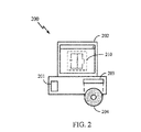
- FIGURE 2 is a block diagram illustrating a design workstation used for circuit, layout, and logic design of the disclosed semiconductor integrated circuit.
- a design workstation 200 includes a hard disk 201 containing operating system software, support files, and design software such as CADENCE or ORCAD.
- the design workstation 200 also includes a display 202 to facilitate design of a circuit design 210.
- the circuit design 210 may be the memory circuit as disclosed above.
- a storage medium 204 is provided for tangibly storing the circuit design 210.
- the circuit design 210 may be stored on the storage medium 204 in a file format such as GDSII or GERBER.
- the storage medium 204 may be a CD-ROM, DVD, hard disk, flash memory, or other appropriate device.
- the design workstation 200 includes a drive apparatus 203 for accepting input from or writing output to the storage medium 204.
- Data recorded on the storage medium 204 may specify logic circuit configurations, pattern data for photolithography masks, or mask pattern data for serial write tools such as electron beam lithography.
- the data may further include logic verification data such as timing diagrams or net circuits associated with logic simulations.
- Providing data on the storage medium 204 facilitates the design of the circuit design 210 by decreasing the number of processes for designing semiconductor ICs.
- an MRAM device and method of making the MRAM device utilize as little as two masks to form an MTJ.
- the method is applied substantially to making STT MRAM. This enables potentially large reductions in the cost of imbedding memory in an integrated circuit product.
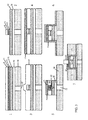
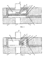
- FIGURE 3 is a schematic process flow of one embodiment of processing used to form an MTJ MRAM structure that may be imbedded in a semiconductor BEOL process.
- An interlevel dielectric, ILD 36 separates MTJ layers from peripheral devices (not shown) that have been previously fabricated in a back-end-of-line (BEOL) process flow.
- An interconnect metallization 37 formed in the ILD 36 provides connection to the control devices (for example, an access transistor associated with an MTJ).
- the interconnect metallization 37 Beginning with a surface including the interconnect metallization 37 and the first ILD 36, a succession of layers are disposed on the surface, including a conductive first electrode 30, a reference fixed magnetic layer stack 32 (including a fixed antiferromagnetic layer and a synthetic antiferro-magnetic layer, neither of which are shown in FIGURE 3 ), a tunnel barrier layer 12, a free layer 11, and a second electrode 6.
- the interconnect metallization 37 connects an MTJ to a source line.
- a conventional dielectric barrier between the ILD 36 and the first contact layer 30 is absent.
- the first electrode 30 may be a refractory metal, such as, for example tantalum (Ta).
- the interconnect metallization 37 may be copper, and tantalum is an excellent barrier material for blocking diffusion of copper into surrounding materials. In other words, tantalum blocks diffusion of metals, such as copper, in the interconnect metallization 37, reducing or eliminating the need for the conventional dielectric barrier.
- depositing a tantalum layer on the ILD 36 and the interconnect metallization 37 is a process friendly integration scheme common to complementary metal oxide semiconductor (CMOS) fabrication.
- CMOS complementary metal oxide semiconductor
- a first mask process is used to etch and pattern various upper layers and electrodes, including the tunnel barrier layer 12, the free layer 11 and the second electrode 6, but not including the reference fixed magnetic layer stack 32.
- removal of a portion of and patterning the reference fixed magnetic layer stack 32 with the first mask may also take place.
- the core MTJ "stack" structure is defined, and includes the tunnel barrier layer 12, the free layer 11 and the conductive second electrode 6.
- a dielectric passivation barrier 40 is disposed over the entire surface, including the MTJ stack.
- the dielectric passivation barrier 40 may be planarized (not shown) using, for example, chemical mechanical polishing (CMP) to expose the conductive second electrode 6.
- CMP chemical mechanical polishing
- a third electrode 15 is deposited over the planarized structure.
- the electrode metallization 15 may be selected from various metals, including refractory metals such as tantalum (Ta).
- a second mask process is used to etch and define the planar dimensions of the components including the third electrode 15, the dielectric passivation barrier 40 (surrounding the second electrode 6, the free layer 11, and the tunnel barrier layer 12), the reference fixed magnetic layer stack 32 and the first electrode 30, down to the surface defined by the ILD 36 and the interconnect metallization 37. It may be noted that alignment of the second mask is not subject to critical dimension registration, and there is considerable latitude in placement of the portions defined by the second mask, provided the second mask is generally positioned over the portions defined by the first mask and the interconnect metallization 37.
- a passivation barrier layer 8 is deposited over the entire surface, including the defined MTJ stack.
- the passivation barrier layer 8, which may be, for example, silicon carbide or silicon nitride, is a very dense film for protecting against penetration by moisture or other species.
- the passivation barrier layer 8, therefore, encapsulates, passivates and protects the MTJ stack.
- the passivation barrier layer 8 is also a dielectric barrier that serves to protect the ILD 36 and can be used as an etch stop in CMOS processes, such as the fabrication of logic circuitry in subsequent BEOL processes. It should be noted that the conventional dielectric barrier reappears here, as the passivation barrier layer 8, but later in the process.
- the passivation barrier layer 8 has an additional function, as described below.
- the various layers of dielectric barriers may be formed, for example, of metal oxides, metal carbides, or metal nitrides.
- the barrier materials may be SiO x , SiC, and SiN. The choice may be made, for example, based on requirements to be susceptible to or resistant to various etchants.
- a second ILD 44 may be deposited to sufficiently bury the resulting structure, and then planarized to expose the passivation barrier layer 8.
- a standard metallization mask - that is now part of a BEOL process, and not specific to the MTJ integration process - is then used to define a trench 42, in the dielectric passivation barrier layer 8 to expose the third electrode 15.
- Another interconnect metallization, 35 such as a bit line interconnect may be disposed in the hole 42 to communicate with the third electrode 15.
- the metal interconnect 35 may be copper or another conductive metal common to the BEOL process flow.
- the ILD 44 separates the MTJ layers from peripheral devices (not shown) that can be fabricated in a subsequent portion of the BEOL process flow.
- the interconnect metalization 35 provides connection to devices fabricated in the subsequent portion of the BEOL process flow.
- the MTJ stack does not have to be critically aligned with the interconnect metallization 37 or 35. That is, the MTJ can be positioned without requiring a registration critical dimension as long the MTJ stack elements 12, 11 and 6 are positioned between the patterned first electrode 30 and the third electrode 15.
- FIGURE 4 in which the MTJ stack is shown centered over the interconnect metallization 37, is only for exemplary illustration. For example, as seen in FIGURE 5 , the MTJ stack can be off-center.
- the first electrode 30 and/or the reference fixed magnetic layer stack 32 may be subsequently planarized, if needed, to provide a sufficiently flat surface for formation of the tunnel barrier layer 12 and the free layer 11 for control of layer thickness and quality, because these two layers (11 and 12) may be on the order of 1 nm.
- the MTJ structure shown in FIGURE 3 may be referred to as an asymmetrical MTJ.
- the first mask is used to form the stack including the conductive second electrode 6, the free layer 11 and the tunnel barrier layer 12, but not the reference fixed magnetic layer stack 32 or the first electrode 30.
- the reference fixed magnetic layer stack 32 and the first electrode 30 are formed using the second mask.
- the same mask set may be used, however, to form an alternative MTJ structure described as "symmetrical.”
- a "symmetric" structure may be achieved by extending the etch process to include the reference fixed magnetic layer stack 32, but not the first electrode 30.
- the first electrode 30 is patterned using the second mask, as before, i.e., in the "asymmetric" configuration.
- the first electrode 30 and the third electrode 15 only are identically patterned to symmetrically sandwich the intervening magnetic tunnel junction elements 32, 12, and 11 and the second electrode 6 between the first electrode 30 and the third electrode 15.
- the reference fixed magnetic layer stack 32 has the same dimensions (apart from thickness) as the tunnel barrier layer 12, the free layer 11 and the conductive electrode 6.
- a first advantage is the elimination of one critical dimension mask.
- a second advantage is that the critical layers of the MTJ stack (i.e., the conductive second electrode 6, the free layer 11, the fixed layer 12 and, optionally, reference fixed magnetic layer stack 32) are self-aligned by being formed in a single mask step.
- a third advantage is the MTJ stack can be placed right over the metallization interconnect 37. This allows a tighter device pitch density.
- a fourth advantage is that the processes are both fewer in number relative to prior art MTJ formation, lowering process costs, and are compatible with integrated circuit BEOL processing. In other words, the processes are "integration friendly.”
- An additional advantage is the formation of a design structure for integrating STT MRAM fabrication processes in a BEOL semiconductor integrated circuit design system that may operate on a computer workstation by executing design operations according to operating system software, support files, and design software such as CADENCE or ORCAD.
- MRAM as set forth in the disclosure may operate with logic circuitry such as microprocessors.
- the MRAM may be integrated into devices that employ the microprocessors.
- the MRAM may be part of a communications device.
- the MRAM may include other types of circuitry without departing from the scope and spirit of the disclosure.
Landscapes
- Engineering & Computer Science (AREA)
- Computer Hardware Design (AREA)
- Manufacturing & Machinery (AREA)
- Mram Or Spin Memory Techniques (AREA)
- Hall/Mr Elements (AREA)
- Semiconductor Memories (AREA)
Applications Claiming Priority (3)
| Application Number | Priority Date | Filing Date | Title |
|---|---|---|---|
| US4616708P | 2008-04-18 | 2008-04-18 | |
| US12/405,461 US8125040B2 (en) | 2008-04-18 | 2009-03-17 | Two mask MTJ integration for STT MRAM |
| EP09732874.4A EP2277211B1 (en) | 2008-04-18 | 2009-04-15 | Manufacturing method of a magnetic tunnel junction element using two masks |
Related Parent Applications (2)
| Application Number | Title | Priority Date | Filing Date |
|---|---|---|---|
| EP09732874.4A Division-Into EP2277211B1 (en) | 2008-04-18 | 2009-04-15 | Manufacturing method of a magnetic tunnel junction element using two masks |
| EP09732874.4A Division EP2277211B1 (en) | 2008-04-18 | 2009-04-15 | Manufacturing method of a magnetic tunnel junction element using two masks |
Publications (1)
| Publication Number | Publication Date |
|---|---|
| EP2800159A1 true EP2800159A1 (en) | 2014-11-05 |
Family
ID=40791514
Family Applications (2)
| Application Number | Title | Priority Date | Filing Date |
|---|---|---|---|
| EP20140172609 Withdrawn EP2800159A1 (en) | 2008-04-18 | 2009-04-15 | A magnetic tunnel junction element |
| EP09732874.4A Not-in-force EP2277211B1 (en) | 2008-04-18 | 2009-04-15 | Manufacturing method of a magnetic tunnel junction element using two masks |
Family Applications After (1)
| Application Number | Title | Priority Date | Filing Date |
|---|---|---|---|
| EP09732874.4A Not-in-force EP2277211B1 (en) | 2008-04-18 | 2009-04-15 | Manufacturing method of a magnetic tunnel junction element using two masks |
Country Status (7)
| Country | Link |
|---|---|
| US (1) | US8125040B2 (enExample) |
| EP (2) | EP2800159A1 (enExample) |
| JP (3) | JP2011518440A (enExample) |
| KR (1) | KR101200008B1 (enExample) |
| CN (1) | CN102007614B (enExample) |
| TW (1) | TW201007730A (enExample) |
| WO (1) | WO2009129283A1 (enExample) |
Cited By (1)
| Publication number | Priority date | Publication date | Assignee | Title |
|---|---|---|---|---|
| DE102016116301B4 (de) | 2015-10-20 | 2024-02-15 | Taiwan Semiconductor Manufacturing Co. Ltd. | Verfahren zur herstellung eines magnetischen tunnelkontakts mit reduzierten schäden |
Families Citing this family (44)
| Publication number | Priority date | Publication date | Assignee | Title |
|---|---|---|---|---|
| US20100157644A1 (en) * | 2008-12-19 | 2010-06-24 | Unity Semiconductor Corporation | Configurable memory interface to provide serial and parallel access to memories |
| WO2010151857A2 (en) * | 2009-06-26 | 2010-12-29 | Cornell University | Method for forming iii-v semiconductor structures including aluminum-silicon nitride passivation |
| US8558331B2 (en) | 2009-12-08 | 2013-10-15 | Qualcomm Incorporated | Magnetic tunnel junction device |
| US8681536B2 (en) * | 2010-01-15 | 2014-03-25 | Qualcomm Incorporated | Magnetic tunnel junction (MTJ) on planarized electrode |
| JP2011238679A (ja) * | 2010-05-07 | 2011-11-24 | Fujitsu Semiconductor Ltd | 磁気記憶装置の製造方法及び磁気記憶装置 |
| US8722543B2 (en) | 2010-07-30 | 2014-05-13 | Headway Technologies, Inc. | Composite hard mask with upper sacrificial dielectric layer for the patterning and etching of nanometer size MRAM devices |
| US8547736B2 (en) * | 2010-08-03 | 2013-10-01 | Qualcomm Incorporated | Generating a non-reversible state at a bitcell having a first magnetic tunnel junction and a second magnetic tunnel junction |
| US8928100B2 (en) * | 2011-06-24 | 2015-01-06 | International Business Machines Corporation | Spin transfer torque cell for magnetic random access memory |
| US8921959B2 (en) * | 2011-07-26 | 2014-12-30 | Taiwan Semiconductor Manufacturing Company, Ltd. | MRAM device and fabrication method thereof |
| US9202562B2 (en) | 2012-04-18 | 2015-12-01 | Advanced Integrated Memory Inc. | Method to reduce read error rate for semiconductor resistive memory |
| US9047964B2 (en) | 2012-08-20 | 2015-06-02 | Qualcomm Incorporated | Multi-level memory cell using multiple magnetic tunnel junctions with varying MGO thickness |
| US8901687B2 (en) | 2012-11-27 | 2014-12-02 | Industrial Technology Research Institute | Magnetic device with a substrate, a sensing block and a repair layer |
| JP6177986B2 (ja) * | 2013-03-15 | 2017-08-09 | インテル・コーポレーション | 埋め込まれた磁気トンネル接合を含む論理チップ |
| US9172033B2 (en) | 2013-07-03 | 2015-10-27 | Taiwan Semiconductor Manufacturing Company, Ltd. | MRAM device and fabrication method thereof |
| US8988835B1 (en) | 2013-10-14 | 2015-03-24 | International Business Machines Corporation | Contact recording tunnel magnetoresistive sensor with layer of refractory metal |
| CN104882538B (zh) * | 2014-02-28 | 2017-09-22 | 中芯国际集成电路制造(上海)有限公司 | 环型磁性随机存取存储器单元结构的制造方法 |
| KR102149195B1 (ko) | 2014-03-04 | 2020-08-28 | 에스케이하이닉스 주식회사 | 전자 장치 및 그 제조 방법 |
| US9269893B2 (en) * | 2014-04-02 | 2016-02-23 | Qualcomm Incorporated | Replacement conductive hard mask for multi-step magnetic tunnel junction (MTJ) etch |
| CN105206741B (zh) * | 2014-06-23 | 2019-02-12 | 中芯国际集成电路制造(上海)有限公司 | 磁性隧道结单元和制备磁性隧道结单元的方法 |
| US10043967B2 (en) * | 2014-08-07 | 2018-08-07 | Qualcomm Incorporated | Self-compensation of stray field of perpendicular magnetic elements |
| US10256395B2 (en) | 2015-06-19 | 2019-04-09 | Intel Corporation | Capped magnetic memory |
| CN106676532B (zh) * | 2015-11-10 | 2019-04-05 | 江苏鲁汶仪器有限公司 | 金属刻蚀装置及方法 |
| US9853210B2 (en) * | 2015-11-17 | 2017-12-26 | International Business Machines Corporation | Reduced process degradation of spin torque magnetoresistive random access memory |
| US9515252B1 (en) * | 2015-12-29 | 2016-12-06 | International Business Machines Corporation | Low degradation MRAM encapsulation process using silicon-rich silicon nitride film |
| US9805795B2 (en) | 2016-01-08 | 2017-10-31 | Samsung Electronics Co., Ltd. | Zero leakage, high noise margin coupled giant spin hall based retention latch |
| US9711713B1 (en) * | 2016-01-15 | 2017-07-18 | Taiwan Semiconductor Manufacturing Company Ltd. | Semiconductor structure, electrode structure and method of forming the same |
| US10522749B2 (en) | 2017-05-15 | 2019-12-31 | Taiwan Semiconductor Manufacturing Company, Ltd. | Combined physical and chemical etch to reduce magnetic tunnel junction (MTJ) sidewall damage |
| US10043851B1 (en) | 2017-08-03 | 2018-08-07 | Headway Technologies, Inc. | Etch selectivity by introducing oxidants to noble gas during physical magnetic tunnel junction (MTJ) etching |
| US10359699B2 (en) | 2017-08-24 | 2019-07-23 | Taiwan Semiconductor Manufacturing Company, Ltd. | Self-adaptive halogen treatment to improve photoresist pattern and magnetoresistive random access memory (MRAM) device uniformity |
| US10585630B2 (en) | 2017-09-11 | 2020-03-10 | Samsung Electronics Co., Ltd. | Selectorless 3D stackable memory |
| US10038138B1 (en) | 2017-10-10 | 2018-07-31 | Headway Technologies, Inc. | High temperature volatilization of sidewall materials from patterned magnetic tunnel junctions |
| US10134981B1 (en) | 2017-10-20 | 2018-11-20 | Headway Technologies, Inc. | Free layer sidewall oxidation and spacer assisted magnetic tunnel junction (MTJ) etch for high performance magnetoresistive random access memory (MRAM) devices |
| US10879077B2 (en) | 2017-10-30 | 2020-12-29 | Taiwan Semiconductor Manufacturing Company Ltd. | Planarization apparatus and planarization method thereof |
| US10325639B2 (en) | 2017-11-20 | 2019-06-18 | Taiwan Semiconductor Manufacturing Company, Ltd. | Initialization process for magnetic random access memory (MRAM) production |
| US10153427B1 (en) | 2017-12-28 | 2018-12-11 | Headway Technologies, Inc. | Magnetic tunnel junction (MTJ) performance by introducing oxidants to methanol with or without noble gas during MTJ etch |
| CN109994476B (zh) * | 2017-12-29 | 2021-03-16 | 上海磁宇信息科技有限公司 | 一种制备磁性随机存储器阵列单元的方法 |
| US10475991B2 (en) | 2018-02-22 | 2019-11-12 | Taiwan Semiconductor Manufacturing Company, Ltd. | Fabrication of large height top metal electrode for sub-60nm magnetoresistive random access memory (MRAM) devices |
| US10790002B2 (en) | 2018-06-21 | 2020-09-29 | Samsung Electronics Co., Ltd. | Giant spin hall-based compact neuromorphic cell optimized for differential read inference |
| US11296277B2 (en) * | 2018-10-16 | 2022-04-05 | Samsung Electronics Co., Ltd. | Variable resistance memory device having an anti-oxidation layer and a method of manufacturing the same |
| US10971176B2 (en) | 2019-02-21 | 2021-04-06 | International Business Machines Corporation | Tunnel magnetoresistive sensor with adjacent gap having chromium alloy seed layer and refractory material layer |
| US11805704B2 (en) * | 2020-05-08 | 2023-10-31 | International Business Machines Corporation | Via interconnects for a magnetoresistive random-access memory device |
| US11569442B2 (en) | 2020-06-17 | 2023-01-31 | International Business Machines Corporation | Dielectric retention and method of forming memory pillar |
| US12464955B2 (en) | 2021-12-09 | 2025-11-04 | Taiwan Semiconductor Manufacturing Co., Ltd. | Magnetic tunnel junction device and method of forming the same |
| US12588421B2 (en) | 2021-12-13 | 2026-03-24 | International Business Machines Corporation | Memory element with a hardmask stack having different stress levels |
Citations (4)
| Publication number | Priority date | Publication date | Assignee | Title |
|---|---|---|---|---|
| US20040145850A1 (en) * | 2002-11-01 | 2004-07-29 | Nec Corporation | Magnetoresistance device and method of fabricating the same |
| US20040205958A1 (en) * | 2003-04-16 | 2004-10-21 | Grynkewich Gregory W. | Methods for fabricating MRAM device structures |
| EP1689006A2 (en) * | 2005-02-05 | 2006-08-09 | Samsung Electronics Co.,Ltd. | Multi-bit magnetic memory device using spin-polarized current and methods of manufacturing and operating the same |
| EP1860769A1 (en) * | 2005-03-18 | 2007-11-28 | Japan Science and Technology Agency | Microwave transmission line integrated microwave generating element and microwave transmission line integrated microwave detecting element |
Family Cites Families (22)
| Publication number | Priority date | Publication date | Assignee | Title |
|---|---|---|---|---|
| JP5013494B2 (ja) * | 2001-04-06 | 2012-08-29 | ルネサスエレクトロニクス株式会社 | 磁性メモリの製造方法 |
| US6631055B2 (en) * | 2001-06-08 | 2003-10-07 | International Business Machines Corporation | Tunnel valve flux guide structure formed by oxidation of pinned layer |
| US6759263B2 (en) * | 2002-08-29 | 2004-07-06 | Chentsau Ying | Method of patterning a layer of magnetic material |
| JP2004128229A (ja) * | 2002-10-02 | 2004-04-22 | Nec Corp | 磁性メモリ及びその製造方法 |
| KR100615600B1 (ko) * | 2004-08-09 | 2006-08-25 | 삼성전자주식회사 | 고집적 자기램 소자 및 그 제조방법 |
| ATE405950T1 (de) * | 2003-06-24 | 2008-09-15 | Ibm | Selbstausgerichtete leitfähige linien für magnetische direktzugriffsspeicherbausteine auf fet-basis und herstellungsverfahren dafür |
| KR100568512B1 (ko) * | 2003-09-29 | 2006-04-07 | 삼성전자주식회사 | 열발생층을 갖는 자기열 램셀들 및 이를 구동시키는 방법들 |
| US20050090111A1 (en) * | 2003-10-24 | 2005-04-28 | Heon Lee | Magnetic tunnel junction device with etch stop layer and dielectric spacer |
| US7259062B2 (en) * | 2003-10-24 | 2007-08-21 | Hewlett-Packard Development Company, Lp. | Method of making a magnetic tunnel junction device |
| US20050205952A1 (en) * | 2004-03-19 | 2005-09-22 | Jae-Hyun Park | Magnetic random access memory cells having split sub-digit lines having cladding layers thereon and methods of fabricating the same |
| US7105903B2 (en) * | 2004-11-18 | 2006-09-12 | Freescale Semiconductor, Inc. | Methods and structures for electrical communication with an overlying electrode for a semiconductor element |
| US7285836B2 (en) * | 2005-03-09 | 2007-10-23 | Maglabs, Inc. | Magnetic random access memory with stacked memory cells having oppositely-directed hard-axis biasing |
| JP4659518B2 (ja) * | 2005-05-24 | 2011-03-30 | シャープ株式会社 | 磁気抵抗効果素子及びその製造方法 |
| KR100655438B1 (ko) * | 2005-08-25 | 2006-12-08 | 삼성전자주식회사 | 자기 기억 소자 및 그 형성 방법 |
| US7511990B2 (en) * | 2005-09-30 | 2009-03-31 | Everspin Technologies, Inc. | Magnetic tunnel junction temperature sensors |
| JP4991155B2 (ja) * | 2006-01-19 | 2012-08-01 | 株式会社東芝 | 半導体記憶装置 |
| US7732881B2 (en) * | 2006-11-01 | 2010-06-08 | Avalanche Technology, Inc. | Current-confined effect of magnetic nano-current-channel (NCC) for magnetic random access memory (MRAM) |
| JP4560025B2 (ja) * | 2006-09-29 | 2010-10-13 | 株式会社東芝 | 磁気ランダムアクセスメモリ及びその製造方法 |
| US7852662B2 (en) * | 2007-04-24 | 2010-12-14 | Magic Technologies, Inc. | Spin-torque MRAM: spin-RAM, array |
| US7723128B2 (en) * | 2008-02-18 | 2010-05-25 | Taiwan Semiconductor Manufacturing Company, Ltd. | In-situ formed capping layer in MTJ devices |
| US8057925B2 (en) * | 2008-03-27 | 2011-11-15 | Magic Technologies, Inc. | Low switching current dual spin filter (DSF) element for STT-RAM and a method for making the same |
| US20090251950A1 (en) * | 2008-04-08 | 2009-10-08 | Ulrich Klostermann | Integrated Circuit, Memory Cell Arrangement, Thermal Select Magneto-Resistive Memory Cell, Method of Operating a Thermal Select Magneto-Resistive Memory Cell, and Method of Manufacturing a Thermal Select Magneto-Resistive Memory Cell |
-
2009
- 2009-03-17 US US12/405,461 patent/US8125040B2/en active Active
- 2009-04-15 WO PCT/US2009/040612 patent/WO2009129283A1/en not_active Ceased
- 2009-04-15 CN CN200980112999.6A patent/CN102007614B/zh not_active Expired - Fee Related
- 2009-04-15 JP JP2011505157A patent/JP2011518440A/ja not_active Withdrawn
- 2009-04-15 KR KR1020107025861A patent/KR101200008B1/ko not_active Expired - Fee Related
- 2009-04-15 EP EP20140172609 patent/EP2800159A1/en not_active Withdrawn
- 2009-04-15 EP EP09732874.4A patent/EP2277211B1/en not_active Not-in-force
- 2009-04-17 TW TW098112861A patent/TW201007730A/zh unknown
-
2014
- 2014-04-03 JP JP2014077077A patent/JP2014160839A/ja not_active Withdrawn
-
2015
- 2015-02-18 JP JP2015029705A patent/JP2015144287A/ja active Pending
Patent Citations (4)
| Publication number | Priority date | Publication date | Assignee | Title |
|---|---|---|---|---|
| US20040145850A1 (en) * | 2002-11-01 | 2004-07-29 | Nec Corporation | Magnetoresistance device and method of fabricating the same |
| US20040205958A1 (en) * | 2003-04-16 | 2004-10-21 | Grynkewich Gregory W. | Methods for fabricating MRAM device structures |
| EP1689006A2 (en) * | 2005-02-05 | 2006-08-09 | Samsung Electronics Co.,Ltd. | Multi-bit magnetic memory device using spin-polarized current and methods of manufacturing and operating the same |
| EP1860769A1 (en) * | 2005-03-18 | 2007-11-28 | Japan Science and Technology Agency | Microwave transmission line integrated microwave generating element and microwave transmission line integrated microwave detecting element |
Cited By (1)
| Publication number | Priority date | Publication date | Assignee | Title |
|---|---|---|---|---|
| DE102016116301B4 (de) | 2015-10-20 | 2024-02-15 | Taiwan Semiconductor Manufacturing Co. Ltd. | Verfahren zur herstellung eines magnetischen tunnelkontakts mit reduzierten schäden |
Also Published As
| Publication number | Publication date |
|---|---|
| TW201007730A (en) | 2010-02-16 |
| CN102007614A (zh) | 2011-04-06 |
| KR101200008B1 (ko) | 2012-11-12 |
| EP2277211B1 (en) | 2014-10-08 |
| KR20110002864A (ko) | 2011-01-10 |
| JP2014160839A (ja) | 2014-09-04 |
| EP2277211A1 (en) | 2011-01-26 |
| CN102007614B (zh) | 2014-07-16 |
| US8125040B2 (en) | 2012-02-28 |
| WO2009129283A1 (en) | 2009-10-22 |
| US20090261437A1 (en) | 2009-10-22 |
| JP2011518440A (ja) | 2011-06-23 |
| JP2015144287A (ja) | 2015-08-06 |
Similar Documents
| Publication | Publication Date | Title |
|---|---|---|
| US8125040B2 (en) | Two mask MTJ integration for STT MRAM | |
| US9159910B2 (en) | One-mask MTJ integration for STT MRAM | |
| US8564079B2 (en) | STT MRAM magnetic tunnel junction architecture and integration | |
| US10522740B2 (en) | Techniques for MRAM MTJ top electrode to metal layer interface including spacer | |
| US9082962B2 (en) | Magnetic Tunnel Junction (MTJ) on planarized electrode | |
| US20230172073A1 (en) | Tall bottom electrode structure in embedded magnetoresistive random-access memory |
Legal Events
| Date | Code | Title | Description |
|---|---|---|---|
| PUAI | Public reference made under article 153(3) epc to a published international application that has entered the european phase |
Free format text: ORIGINAL CODE: 0009012 |
|
| 17P | Request for examination filed |
Effective date: 20140616 |
|
| AC | Divisional application: reference to earlier application |
Ref document number: 2277211 Country of ref document: EP Kind code of ref document: P |
|
| AK | Designated contracting states |
Kind code of ref document: A1 Designated state(s): AT BE BG CH CY CZ DE DK EE ES FI FR GB GR HR HU IE IS IT LI LT LU LV MC MK MT NL NO PL PT RO SE SI SK TR |
|
| RIN1 | Information on inventor provided before grant (corrected) |
Inventor name: KANG, SEUNG. H Inventor name: NOWAK, MATTHEW M. Inventor name: LI, XIA Inventor name: GU, SHIQUN |
|
| R17P | Request for examination filed (corrected) |
Effective date: 20150501 |
|
| RBV | Designated contracting states (corrected) |
Designated state(s): AT BE BG CH CY CZ DE DK EE ES FI FR GB GR HR HU IE IS IT LI LT LU LV MC MK MT NL NO PL PT RO SE SI SK TR |
|
| 17Q | First examination report despatched |
Effective date: 20150805 |
|
| STAA | Information on the status of an ep patent application or granted ep patent |
Free format text: STATUS: THE APPLICATION IS DEEMED TO BE WITHDRAWN |
|
| 18D | Application deemed to be withdrawn |
Effective date: 20151216 |