EP2786425B1 - Diode p/n à hétérostructure controlée autopositionnée sur hgcdte pour imageurs infrarouges - Google Patents
Diode p/n à hétérostructure controlée autopositionnée sur hgcdte pour imageurs infrarouges Download PDFInfo
- Publication number
- EP2786425B1 EP2786425B1 EP12790573.5A EP12790573A EP2786425B1 EP 2786425 B1 EP2786425 B1 EP 2786425B1 EP 12790573 A EP12790573 A EP 12790573A EP 2786425 B1 EP2786425 B1 EP 2786425B1
- Authority
- EP
- European Patent Office
- Prior art keywords
- cadmium
- diode
- junction
- doped
- concentration
- Prior art date
- Legal status (The legal status is an assumption and is not a legal conclusion. Google has not performed a legal analysis and makes no representation as to the accuracy of the status listed.)
- Active
Links
Images


Classifications
-
- H—ELECTRICITY
- H10—SEMICONDUCTOR DEVICES; ELECTRIC SOLID-STATE DEVICES NOT OTHERWISE PROVIDED FOR
- H10F—INORGANIC SEMICONDUCTOR DEVICES SENSITIVE TO INFRARED RADIATION, LIGHT, ELECTROMAGNETIC RADIATION OF SHORTER WAVELENGTH OR CORPUSCULAR RADIATION
- H10F30/00—Individual radiation-sensitive semiconductor devices in which radiation controls the flow of current through the devices, e.g. photodetectors
- H10F30/20—Individual radiation-sensitive semiconductor devices in which radiation controls the flow of current through the devices, e.g. photodetectors the devices having potential barriers, e.g. phototransistors
- H10F30/21—Individual radiation-sensitive semiconductor devices in which radiation controls the flow of current through the devices, e.g. photodetectors the devices having potential barriers, e.g. phototransistors the devices being sensitive to infrared, visible or ultraviolet radiation
- H10F30/22—Individual radiation-sensitive semiconductor devices in which radiation controls the flow of current through the devices, e.g. photodetectors the devices having potential barriers, e.g. phototransistors the devices being sensitive to infrared, visible or ultraviolet radiation the devices having only one potential barrier, e.g. photodiodes
- H10F30/221—Individual radiation-sensitive semiconductor devices in which radiation controls the flow of current through the devices, e.g. photodetectors the devices having potential barriers, e.g. phototransistors the devices being sensitive to infrared, visible or ultraviolet radiation the devices having only one potential barrier, e.g. photodiodes the potential barrier being a PN homojunction
- H10F30/2212—Individual radiation-sensitive semiconductor devices in which radiation controls the flow of current through the devices, e.g. photodetectors the devices having potential barriers, e.g. phototransistors the devices being sensitive to infrared, visible or ultraviolet radiation the devices having only one potential barrier, e.g. photodiodes the potential barrier being a PN homojunction the devices comprising active layers made of only Group II-VI materials, e.g. HgCdTe infrared photodiodes
-
- H—ELECTRICITY
- H10—SEMICONDUCTOR DEVICES; ELECTRIC SOLID-STATE DEVICES NOT OTHERWISE PROVIDED FOR
- H10F—INORGANIC SEMICONDUCTOR DEVICES SENSITIVE TO INFRARED RADIATION, LIGHT, ELECTROMAGNETIC RADIATION OF SHORTER WAVELENGTH OR CORPUSCULAR RADIATION
- H10F30/00—Individual radiation-sensitive semiconductor devices in which radiation controls the flow of current through the devices, e.g. photodetectors
- H10F30/20—Individual radiation-sensitive semiconductor devices in which radiation controls the flow of current through the devices, e.g. photodetectors the devices having potential barriers, e.g. phototransistors
- H10F30/21—Individual radiation-sensitive semiconductor devices in which radiation controls the flow of current through the devices, e.g. photodetectors the devices having potential barriers, e.g. phototransistors the devices being sensitive to infrared, visible or ultraviolet radiation
- H10F30/22—Individual radiation-sensitive semiconductor devices in which radiation controls the flow of current through the devices, e.g. photodetectors the devices having potential barriers, e.g. phototransistors the devices being sensitive to infrared, visible or ultraviolet radiation the devices having only one potential barrier, e.g. photodiodes
- H10F30/222—Individual radiation-sensitive semiconductor devices in which radiation controls the flow of current through the devices, e.g. photodetectors the devices having potential barriers, e.g. phototransistors the devices being sensitive to infrared, visible or ultraviolet radiation the devices having only one potential barrier, e.g. photodiodes the potential barrier being a PN heterojunction
-
- H—ELECTRICITY
- H10—SEMICONDUCTOR DEVICES; ELECTRIC SOLID-STATE DEVICES NOT OTHERWISE PROVIDED FOR
- H10F—INORGANIC SEMICONDUCTOR DEVICES SENSITIVE TO INFRARED RADIATION, LIGHT, ELECTROMAGNETIC RADIATION OF SHORTER WAVELENGTH OR CORPUSCULAR RADIATION
- H10F71/00—Manufacture or treatment of devices covered by this subclass
- H10F71/125—The active layers comprising only Group II-VI materials, e.g. CdS, ZnS or CdTe
- H10F71/1253—The active layers comprising only Group II-VI materials, e.g. CdS, ZnS or CdTe comprising at least three elements, e.g. HgCdTe
-
- H—ELECTRICITY
- H10—SEMICONDUCTOR DEVICES; ELECTRIC SOLID-STATE DEVICES NOT OTHERWISE PROVIDED FOR
- H10F—INORGANIC SEMICONDUCTOR DEVICES SENSITIVE TO INFRARED RADIATION, LIGHT, ELECTROMAGNETIC RADIATION OF SHORTER WAVELENGTH OR CORPUSCULAR RADIATION
- H10F77/00—Constructional details of devices covered by this subclass
- H10F77/10—Semiconductor bodies
- H10F77/12—Active materials
- H10F77/123—Active materials comprising only Group II-VI materials, e.g. CdS, ZnS or HgCdTe
- H10F77/1237—Active materials comprising only Group II-VI materials, e.g. CdS, ZnS or HgCdTe having at least three elements, e.g. HgCdTe
Definitions
- the present invention relates to the field of diodes manufactured in semiconductor materials. More specifically, the invention relates to p / n type diodes formed in substrates based on materials of the type Hg 1-x Cd x Te, and which can be used for infrared imagers.
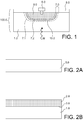
- the p / n diodes are generally formed in a substrate 100.0 having predominantly n-doping. They comprise in this substrate 100.0 an n doping region, called sole 1.0 ( figure 1 ) and a doped zone p + p doping, adjacent to the insole 1.0.
- the interface between the doping region n 1.0 and the p + doped zone 9.0 is commonly called the "p / n junction" 10.0.
- a space charge area 7.0 is formed on either side of the 10.0 p / n junction.
- the doped pad 1.0 is positively charged and at a second limit 7.2 of the space charge area, the p + doped area 9.0 is negatively charged inducing an electric field. intense.
- an electromagnetic wave W enters the substrate by the soleplate 1.0, it forms an electron-hole pair by interaction with atoms of the material of the soleplate 1.0.
- a minority carrier in the sole here a hole, diffuses a hole diffusion length in the sole 1.0 before recombining with a majority carrier, here an electron. If the minority carrier diffuses into the 7.0 space charge area, it does not recombine immediately. It is accelerated by the electric field towards the p + doped zone 9.0. It recombines therein forming an inverse current between the p + doped zone 9.0 and the n doping soleplate 1.0.
- the electromagnetic wave W passes through the soleplate 1.0 and the generation of the electron-hole pair takes place in the space charge area 7.0, the pair is instantly separated by the electric field.
- the hole is directed to the second limit 7.2 and to the p + doped zone 9.0 and the electron to the first limit 7.1 and to the n doping soleplate 1.0.
- This phenomenon is rarer than the previous one, and generally requires that the soleplate 1.0 must be very thin, the electromagnetic wave W must pass through the entire soleplate 1.0.
- a p / n diode is sensitive only to wavelengths whose energy is sufficient to cross the gap of the material of the soleplate 1.0 to an electron to form electron / hole pairs. It is therefore necessary that an electromagnetic wave has a minimum energy to be detected. Conversely, if the electromagnetic wave has an energy much greater than the gap, the electromagnetic wave interacts strongly with the plate 1.0 and the majority of the electron-hole pairs are formed too far from the p / n junction and the holes recombine with one another. majority carrier without allowing a detection of the wave.
- the gap of the material of the soleplate 1.0 defines a minimum wavelength that can be sensed by the diode and a range of wavelengths that can be optimally detected.
- the gap of the material depends on the concentration of cadmium in the soleplate 1.0.
- a low concentration of cadmium ensures a small gap in the diode and the detection of long wave electromagnetic waves.
- a small gap induces an increased sensitivity of the diode to defects and a larger dark current.
- the gap is artificially reduced in a few localized points of the material. In a small gap material this artificial reduction is larger proportionally to the gap.
- the dark current is an imperfection of photodiodes caused by thermal agitation. To some extent, thermal agitation can provide sufficient energy for some electrons to form an electron-hole pair by spontaneous generation. If the hole formed by spontaneous generation appears in the area space charge or near the junction p / n, there is formation of a current in the absence of incident electromagnetic wave on the diode.
- heterostructure diodes As illustrated in FIG. figure 2G , one possibility is to manufacture so-called “heterostructure” diodes as illustrated in FIG. figure 2G .
- Such a structure and a method for manufacturing it are described in the article "MBE HgCdTe Planar Infrared Photodiodes p-on-n Heterostructure” by JM Arias et al. published in 1993 in "Journal of Electronic Materials", volume 22, number 8, pages 1049 to 1053 .
- the manufacture of a heterostructure diode means that a p / n diode will be formed, having a 10.0 p / n junction and a 7.0 space charge area around it, such as the 1.0 footing of the diode.
- the diode either in a material having a small gap, but that the junction p / n 10, or in particular the second limit 7.2 of the space charge area 7.0 is in a material having a larger gap.
- the spontaneous generation of electron-hole pairs in the space charge area 7.0 is reduced, since the energy to be supplied to form an electron-hole pair is larger than in the baseplate 1.0. Then the diode is less sensitive to defects and dark current.
- the junction p / n 10.0 must then be located sufficiently close to the soleplate 1.0 having a small gap, more particularly so that the first limit 7.1 of the space charge area 7.0 is in the insole 1.0 with a small gap.
- the diode is such that the majority of the p + doped region 9.0 is in a portion of the substrate 100.0 having a higher cadmium concentration than the soleplate 1.0 without being in the passivation layer 5.0, one of the elements of which is Cadmium Cd.
- Such a configuration leads the diode to be able to pick up a range of wavelengths comprising weak wavelengths, depending on the gap of the soleplate 1.0, while being less sensitive to noise, the dark current and the defects that a diode without heterostructure.
- a substrate 100.0 in which the soleplate 1.0 is formed of a layer of base of the type Hg 1-x Cd x Te, with "x" equal for example 0.22, and a surface layer 2.0, in Hg 1-y Cd y Te where "y" has a value greater than that of " x ", for example 0.28, in contact with the soleplate 1.0.
- the 2.0 surface layer has a larger gap than the 1.0 sole.
- Heterojunction 3.0 is the interface between the soleplate 1.0 and the surface layer 2.0.
- a doped p + doped region 9.0 is then formed in the surface layer 2.0 so that the p + doped area 9.0 has a thickness greater than that of the surface layer 2.0 and slightly exceeds the heterojunction 3.0.
- a 10.0 p / n junction is defined by an interface between the p + doped zone 9.0 and the n-doped baseplate 1.0.
- the p / n junction 10.0 protrudes from the surface layer 2.0 so that at least the first limit 7.1 of the space charge area 7.0 is located in the baseplate 1.0.
- the p / n junction 10.0 is then positioned in an area of the baseplate 1.0 in which cadmium of the surface layer 2.0 may have slightly diffused.
- a diode based on Hg 1-x Cd x Te is covered with a passivation layer 5.0 of which is elements is cadmium Cd, to stabilize the diode.
- a conductive contact 6.0 is present in the p + doped area 9.0 to recover any current produced in the diode.
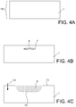
- an initial substrate is selected which forms a soleplate 1.0 in Hg 1-x Cd x Te ( Figure 2A ).
- the value of "x" can be for example 0.22. This value is chosen so that the gap of the Hg 1-x Cd x Te is the gap required to detect given electromagnetic waves which have a minimum energy corresponding to this gap.
- the soleplate 1.0 can typically have a thickness of a few tenths of a micrometer to a few tens of micrometers, for example 10 microns.
- the soleplate 1.0 initially comprises a doping n established by means of one or more dopants of the donor type, introduced during its manufacture. Without introduction of extrinsic dopants, the soleplate 1.0 can be n or p type.
- the surface layer 2.0 may have a thickness of, for example, 1 ⁇ m. It forms a 100.0 substrate with the 1.0 sole.
- the interface 3.0 between the insole 1.0 and the surface layer 2.0 is called heterojunction 3.0.
- an acceptor type dopant 8.0 is introduced into an area to be doped located in the surface layer 2.0 by means of ion implantation ( Figure 2C ).
- the ion implant implants the dopant 8.0 at a given depth in the form of dopant atoms, and forms an implantation zone 70.0 containing the dopant 8.0.
- the dopant 8.0 is carried out a diffusion of the dopant 8.0. Diffusion displaces the dopant atoms and thus creates a conventional doping region form for a p / n diode ( 2D figure ). Then activation of the dopant 8.0 takes place, this activation causes the dopant atoms to be introduced into the crystal lattice of the soleplate 1.0.
- the activation of a dopant such as arsenic displaces the arsenic atoms in substitution for tellurium atoms in the superficial layer 2.0 and in the soleplate 1.0.
- the activation leads to the formation of a p + doped zone 9.0.
- the diffusion and activation of the dopant are generally grouped into a single diffusion and activation step.
- This diffusion and activation step is optimized to diffuse the dopant until the interface between the p + doped zone 9.0 and the remainder of the superficial layer 2.0 and the soleplate 1.0 is positioned near the heterojunction. 3.0. This interface extends beyond the 2.0 surface layer in the 1.0 footing. A junction p + / n 10.0 will be formed at this interface as will be explained later.
- this diffusion and activation step causes the formation of mercury gaps, which doping, with p-type doping, the entire substrate 100.0, sole 1.0, surface layer 2.0 and p + doped zone 9.0 inclusive.
- the interface between the p + doped zone 9.0 and the remainder of the soleplate 1.0 and the surface layer 2.0 becomes a p + / p junction. For the sake of simplification, we will call this junction interface p / n 10.0.
- junction p / n 10.0 in the insole 1.0, at the limit of the heterojunction 3.0, so that the junction p / n 10.0 is in an area having an intermediate cadmium concentration between that of the soleplate 1.0 and that of the surface layer 2.0.
- a passivation layer 5.0 one of whose elements is cadmium Cd, is deposited on top of the surface layer 2.0 ( figure 2E ). This layer has the advantage of protecting the structure of the diode p / n.
- the person skilled in the art knows how to proceed with a step of filling in the mercury gaps following the steps previously described.
- the purpose of the mercury gap filling step is to cancel the p-doping induced by the formation of defects during the ion implantation and the dopant diffusion and activation step.
- the sole 1 with a donor-type dopant regains an n-type doping ( figure 2F ).
- the junction p + / p then becomes a junction p + / n 10.0 commonly called junction p / n.
- a conductive contact 6.0 preferably metallic ( figure 2G ). This contact passes through the passivation layer 5.0 and enters the p + doped zone 9.0 without reaching the soleplate 1.0.
- the conductive contact 6.0 can be formed by conventional techniques in microelectronics. It is then connected to an external electrical circuit not shown. Unrepresented secondary contacts are generally formed outside the diode and are intended to create an electrical contact between the n-doped baseplate 1.0 and the external electrical circuit. The two types of contacts working together can be used to recover any current that may appear at the junction p / n 10.0 for example under the influence of an electromagnetic wave.
- a second limitation is that the heterojunction 3.0 is present on the entire substrate 100.0.
- a third limitation lies in the fact that the relative position of the p / n 10.0 junction with respect to the heterojunction depends on the diffusion of the dopant and in particular on the conditions of the implantation and the conditions of the diffusion annealing and activating the dopant. Implantation and diffusion of dopants is a random and statistical phenomenon that is difficult to master finely.
- the junction p / n 10.0 is advantageously located in the soleplate 1.0, close to the surface layer 2.0, where there is a cadmium concentration gradient.
- a small difference in the depth of the p / n junction 10.0 between two adjacent diodes leads to the junction p / n 10.0 being at a different point of the gradient and therefore with a different cadmium concentration at the junction p / n 10.0 .
- the p / n junction 10.0 can therefore be positioned in a different gap material from one diode to another.
- the exact concentration of cadmium at the junction p / n 10.0 is difficult to predict and control.
- the performance of the diode for example the quantum efficiency, the dark current or the range of wavelengths can thus vary from diode to diode. So there is a risk of not obtaining the same signal for the same radiative flow from one diode to another.
- a p / n junction heterostructure diode according to the invention and the method according to the invention aim to reduce the impact of these limitations. In particular, they aim to produce a better quality heterojunction at a lower cost, to facilitate the control of a relative position of the p / n junction with respect to the heterojunction and to improve the reproducibility and repeatability of this relative position.
- a substrate to another and a diode to another in the same substrate aim to reduce the impact of these limitations. In particular, they aim to produce a better quality heterojunction at a lower cost, to facilitate the control of a relative position of the p / n junction with respect to the heterojunction and to improve the reproducibility and repeatability of this relative position.
- the substrate is n-doped by introduction of extrinsic donors.
- the device according to the invention is characterized in that the concentrated part is located only in the p + doped zone and forms a substantially constant cadmium concentration box.
- the concentrated part is located only in the p + doped zone and forms a substantially constant cadmium concentration box.
- Such a device makes it possible to solve the aforementioned problems. Indeed, since the heterostructure is contained in the p + doped zone, it is not present in the substrate outside the diode (s) of the device. Thus, there can be no problems related to the heterostructure between two neighboring diodes.
- the first part, having a first concentration of cadmium is accessible to undergo treatment around the diodes, without being covered by a layer superficial having another concentration of cadmium as is the case in the structures of the state of the art.
- the box has a bottom located at a substantially constant average distance relative to the p / n junction.
- a device according to the invention allows a control of the performance of the diode, with a reduction in variations of average relative distance vis-à-vis the state of the art.
- the box of the two neighboring diodes are disjoint and the average relative distance in one of the two diodes is substantially equal to the average relative distance in the another diode, ensuring a relative position between the p / n junction and the substantially identical heterojunction for each diode and a reliability of performance for each diode.
- each diode having a substantially identical relative position between the junction p / n and the heterojunction, the performance of each diode are substantially identical.
- the p + doped zone is doped with an acceptor dopant which is advantageously arsenic.
- Hg 1-x Cd x Te with x having a value preferably between 0.15 and 0.95, for example 0.3.
- This value of x translates a value of the first cadmium concentration and makes it possible to calculate it.
- the value of x is substantially equal to twice the value of the first concentration of cadmium.
- the box is in Hg 1-y Cd y Te with y having a value advantageously between 0.15 and 0.95, strictly greater than the value of x.
- the value of y translates a value of the second concentration of cadmium and makes it possible to calculate it. These values of x and y ensure that the diodes will be sensitive to wavelengths in an infrared spectrum.
- the value of y is substantially equal to twice the value of the second concentration.
- the values of x and y are not too large. In particular, this difference is less than 0.5 or 0.2. If the deviation of the values between x and y was too great, it could form a large gap gap between the sole and any conductive contact. This large gap gap should then be crossed by any hole resulting from an interaction between the electromagnetic wave and the sole. This could induce in some cases a decrease in efficiency of the detection device or an increase in the power consumed.
- the soleplate is thus defined in step a) as a part of the substrate in which there is no acceptor dopant.
- the method according to the invention is characterized in that it comprises, preferentially before step d) and preferably after step b) and step c), a step of selective inter-diffusion of cadmium from the layer of passivation in the p + doped zone.
- a first part in Hg 1-x Cd x Te, of first concentration in cadmium, and a second part in Hg 1-y Cd y Te, called box or concentrated part, having a second concentration of cadmium are formed. constant and superior to the first cadmium concentration of the sole.
- the box is located inside the p + doped zone.
- the box is circumscribed within an area delimited by the p / n junction.
- the step of selective diffusion of the process according to the invention makes it possible to form, automatically and without the need for external control, a second portion, concentrated in cadmium, located in an optimized manner vis-à-vis the doped region p + and autoposition Avenue. Since the scattering is selective, it is controlled by operating conditions of the selective inter-scattering step and by the shape of the p + doped zone, and thus a control of the p + doped zone shape leads to control of the box. . There is therefore no risk of obtaining a heterostructure inappropriately positioned with respect to the p / n junction, the p / n junction being defined as being a boundary between the p + doped zone and the doped sole. not.
- the box, more concentrated in cadmium, being obtained by cadmium diffusion in an initial crystal lattice has a crystal lattice identical to an initial crystal lattice of the substrate.
- step b) of diffusion and activation of the dopant is performed before step c) of depositing the passivation layer.
- the step of selective diffusion of cadmium advantageously comprises a selective diffusion annealing. This is preferably carried out at a temperature greater than 100 ° C and for a time greater than one minute under conditions of pressure and temperature which limit the degradation of the material.
- the diffusion of the cadmium in the p + doped zone is thus controlled by the temperature and the duration of the annealing, which are two parameters influencing the operating conditions of the selective inter-diffusion step. These parameters are identical for the entire substrate and are easily repeatable during manufacture of other devices according to the invention.
- the cadmium diffusion is substantially identical vis-à-vis the p + doped zone and even if from one diode to another the p + doped zones have substantially different shapes.
- the p / n junction and the box are arranged with a substantially identical relative position for any diode of the same substrate or any substrate having underwent diffusion annealing under the same operating conditions.
- the acceptor dopant is preferably arsenic.
- the ion implantation can take place with a dose typically between 10 12 and 10 16 at / cm 2 .
- the well created by the method according to the invention, has boundaries that form an interface, called heterojunction, with the rest of the substrate having the first concentration of cadmium. Since the box is included inside the p + doped zone, the heterojunction is also included inside the p + doped zone.
- the box having a bottom and the method for producing simultaneously several p / n diodes, the heterojunction, at the bottom of the box, is at a relative average distance of the junction p / n substantially identical for all the diodes manufactured during the process, inside the p + doped zone.
- the process according to the invention is such that, by controlling the temperature and the duration of the inter-diffusion step, it is possible to precisely and repeatedly position the heterojunction with respect to at the junction p / n.
- the substrate in its entirety has a concentration of cadmium which is the first concentration.
- concentration of cadmium which is the first concentration.
- HgCdTe there is no surface layer of cadmium concentration HgCdTe different from that of the substrate as it exists in the prior art.
- the method according to the invention therefore allows significant financial gains because it is possible to manufacture heterostructure diodes without the need for a substrate having an epitaxial layer, which requires for its manufacture a long and expensive treatment and which moreover can induce a creation of defects.
- the invention relates firstly to a device comprising at least one p / n diode with a heterostructure. Such a device according to the invention is illustrated in figure 3 .
- x is advantageously between 0.15 and 0.25, for example 0.22, if it is desired to form a diode sensitive to long wavelength infrared electromagnetic waves known in English under the name of LWIR ("long wavelength infra-red") in particular between 9 microns and 30 microns.
- LWIR long wavelength infra-red
- x is advantageously between 0.25 and 0.4, for example 0.3, if it is desired to form a diode sensitive to infrared electromagnetic waves at average wavelengths, known in English under the name MWIR ("Mid-wavelength infra-red”) in particular between 3 microns and 9 microns.
- MWIR Mod-wavelength infra-red
- x is advantageously between 0.4 and 0.95, for example 0.45, if it is desired to form a diode sensitive to short-wavelength infrared electromagnetic waves known in English under the name short wavelength infra-red (SWIR), in particular between 0.8 and 3 ⁇ m.
- SWIR short wavelength infra-red
- the value of x is substantially equal to 0.3.
- the sole 1 comprises on one side a doping region p forming a p + doped zone 9 which is not in contact with the possible substrate.
- the p + doped zone 9 is doped by means of an acceptor type dopant for the Hg 1-x Cd x Te.
- Arsenic (As) is an advantageous dopant of this type.
- Other acceptor-type dopants that may be used are, for example, phosphorus (P), antimony (Sb), bismuth (Bi), or other atoms. These dopants, as well as arsenic, are positioned in substitution for a tellurium atom during a dopant activation step.
- Lithium (Li), copper (Cu) or gold (Au), positioned in substitution of a cadmium or mercury atom, are also acceptor dopants that can be used in the context of the invention.
- acceptor dopants Lithium (Li), copper (Cu) or gold (Au), positioned in substitution of a cadmium or mercury atom.
- the p + doped zone 9 has a shape comparable to those found in the state of the art, both for p / n diodes with a heterostructure, and for p / n diodes without heterostructure.
- the p + doped zone 9 is therefore in contact with the passivation layer 5.
- the p + doped zone 9 moreover extends more finely in the sole 1, according to a conventional dopant diffusion profile, for example up to about 1 depth of the midsole 1.
- the interface between the p + doped zone 9 and the n-doped inset 1 forms a p + / n junction called p / n junction 10.
- a conductive contact 6 which passes through the passivation layer 5 and enters the p + doped zone 9, in the same way as in a diode according to the state of the art.
- the concentrated portion 11 is in the form of a box 12 of substantially constant concentration of cadmium, having limits with the rest of the substrate located at the junction p / n 10.
- the substrate therefore comprises a heterostructure composed of the sole 1 in which is inserted at least a box 12 in Hg 1-y Cd y Te strictly more concentrated in cadmium than the sole 1.
- the heterojunction 3 is substantially located at the junction p / n, but is still located substantially within the p + doped zone 9. Indeed, advantageously, the heterojunction 3 is not superimposed with the junction p / n, but found entirely inside zone 9 doped p +. There is therefore a part of the p + doped zone 9 which is not at the second concentration.
- the composition is between 0.15 and 0.95, for example 0.5.
- the cadmium composition of the concentrated portion 11 is preferably substantially constant.
- the value of y is within the same range of values as x.
- the value of y may, however, be in a range other than x, among those mentioned above, if the difference between the values of x and y is not too great. In particular, this difference is typically less than 0.5. We will make sure that the difference between x and y is not larger. Otherwise, it could be formed a large gap gap between the sole and any conductive contact present in the diode. This large gap gap would then need to be crossed by any hole resulting from an interaction between the electromagnetic wave and the sole. This could induce a decrease in the efficiency of the detection device or an increase in the power consumed.
- the substrate according to the invention then comprises, as a first approximation, a first portion 4 of first cadmium concentration, comprising the insole 1, doped n, and a portion of the p + doped zone 9 which is not at the second concentration.
- an intermediate zone having an intermediate cadmium concentration between the first concentration, in the soleplate 1, and the second concentration, in the well 12, is situated at the junction p / n 10, but outside the well 12.
- the intermediate zone preferably extends over at least the part of the p + doped zone 9 which is not at the second concentration.
- This intermediate zone has a cadmium concentration gradient between the first concentration and the second concentration in the form of a conventional diffusion profile.
- a space charge zone not shown, is formed around the junction p / n 10, the space charge zone is mainly in a material having either the intermediate concentration , the second concentration, that is to say that it has a higher concentration of cadmium than the first concentration. Consequently, the space charge zone is in a material that has a larger gap than the gap of the material of the soleplate 1.
- the junction p / n is such that a first limit of the charge area d space is in the sole 1 or part of the intermediate zone having a cadmium concentration close to that of the sole 1 and a second limit of the space charge zone is in the chamber 12 or in a part of the intermediate zone having a cadmium concentration close to that of the caisson 12.
- the caisson 12 having a bottom, the heterojunction 3 formed by the boundaries of the caisson 12 and the p / n junction 10 formed by the boundaries of the p + doped zone 9 are spaced apart on average at the bottom of the caisson 12. a given average distance.
- the heterojunction 3 and the p / n junction 10 then have a given relative position. If there are several diodes p / n in the device according to the invention, the relative positions of heterojunctions 3 and p / n junctions are substantially identical for all the diodes manufactured during the process.
- a heterostructure 3 which reduces the noise in the p / n diode.
- the heterojunction 3 is present in the device only near the p / n junction 10 and the heterojunction is fabricated without forming interface defects.
- the invention also relates to a method for manufacturing a device according to the invention. Such a method according to the invention is described below in connection with the Figures 4A to 4G .
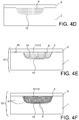
- a substrate 101 which comprises a so-called sole 1 layer of a Hg 1-x Cd x Te type material having a first cadmium concentration and of composition as defined above ( Figure 4A ).
- the sole 1 may have a thickness of several micrometers to a few tens of micrometers, for example 10 microns. It may for example have been formed by molecular beam epitaxy (MBE) or liquid phase epitaxy (EPL).
- the sole 1 initially comprises a doping n formed by an extrinsic dopant dopant introduced during its formation, for example indium.
- This dopant can have a density low, known to those skilled in the art, for example typically between 1.E 14 at / cm 3 and 5.E 16 at / cm 3 . If the dopant is not introduced during the formation of the sole 1, it is added before the steps mentioned below.
- a localized ion implantation of an acceptor-type dopant 8 is carried out ( Figure 4B ) in the form of dopant atoms.
- the dopant may be one of those mentioned above in the description of the device, in particular arsenic.
- Standard implantation conditions are for example an energy of 500 KeV and an implantation dose 2.E 15 at / cm 2.
- Other ion implantation conditions are usable depending on the desired performance for the diode and are known to those skilled in the art.
- the implantation energy may vary between for example 10 KeV and 600 KeV and the implantation dose may vary typically between 10 12 and 10 16 at / cm 2 .
- Dopant 8 is found implanted in an implantation zone 7, buried in the sole 1. There may be a simultaneous implantation of several dopants.
- a step of diffusion and activation of the dopant ( figure 4C ) is preferably performed.
- This step is advantageously accomplished by means of diffusion annealing and dopant activation.
- the dopant atoms then diffuse in three directions: along two directions defining a main surface 13 of the sole 1, and in a direction 13 'perpendicular to this main surface 13.
- mercury gaps form and induce in all the doping substrate p, including in the soleplate 1 initially doped n.
- the dopant atoms are activated. That is, they position themselves to give extra polarity in the material where they are. With the implantation doses generally used, the additional polarity induces p + doping in the material where the dopant diffuses.
- the activation consists in positioning the arsenic dopant atoms in substitution for tellurium atoms.
- the diffusion and activation annealing generally takes place under saturation pressure of mercury, at a temperature preferably between 300 ° C. and 500 ° C., for a period preferably comprised between a few minutes and a few hours. A particular example is a temperature of 440 ° C and a duration of 5 hours. It is understood that those skilled in the art will be able to adapt the time and the temperature of the diffusion annealing and dopant activation according to the type of dopant used, the implantation doses used and the type of use provided for the diode.
- the acceptor dopant atoms may have a density typically between 10 15 and 10 20 at / cm 3.
- a passivation layer 5 of which one of the elements is cadmium Cd is deposited over the sole 1.
- This layer can be obtained by physical vapor deposition (PVD) or by any other technique.
- PVD physical vapor deposition
- This layer has a thickness typically between 0.5 micrometer and 5 micrometers, for example 1 micrometer.
- the doping diffusion and activation annealing is then carried out, if it has not been done before the deposition of the passivation layer 5.
- the inventors propose a step of selective inter-diffusion of cadmium ( figure 4E ).
- This step causes a diffusion of cadmium from the passivation layer 5, rich in cadmium, to the sole 1 and in particular selectively towards the p + doped zone 9 present in the sole 1, p-doped by the mercury vacancies.
- a selective diffusion annealing is advantageously carried out with a temperature greater than 100 ° C.
- the annealing may have a duration greater than one minute.
- the selective diffusion annealing preferably has a temperature below 400 ° C. so as to limit any new diffusion of the dopant.
- the diffusion therefore takes place selectively in the p + doped zone 9, where the carrier density is of the order of 10 17 to 10 20 at / cm 3 , with respect to the remainder of the soleplate 1.
- the soleplate 1 although p-doped, has too low hole density with respect to the intrinsic density of carriers. Diffusion is considered instantaneous throughout the p + doped zone 9, as long as the acceptor dopant density, here arsenic, is greater than n i .
- Cadmium therefore has, in the p + doped zone 9, a selective diffusion length 14 much greater than a standard diffusion length of cadmium, in the p-doped sole plate 1.
- the duration and the temperature of the selective diffusion annealing are adjustable in order to control the selective diffusion length 14 of the cadmium in the p + doped zone 9 as well as the quantity of cadmium that diffuses.
- cadmium diffuses mainly in the p + doped zone.
- a box 12 of Hg 1-y Cd y Te is thus formed, having a second concentration of cadmium, substantially constant, richer in cadmium than the sole 1.
- the interface between the box 12 and the sole 1 is called "heterojunction 3 ". Since cadmium diffuses mainly where the arsenic is present in a quantity greater than the intrinsic density of carriers n i , this means that the well 12 is entirely comprised in the p + doped zone 9 and that the heterojunction 3 does not exceed the junction p / n 10.
- the intermediate zone comprises a cadmium diffusion gradient in the sole, referred to in the invention as "intermediate profile".
- the intermediate zone and the sole 1 are two portions of the substrate which are at a concentration different from the second concentration of cadmium and they together define a first part 4.
- all the boxes 12 different diodes can be considered as belonging to a second part, having a second concentration of cadmium substantially constant at any point.
- Control of the selective diffusion length 14 and the amount of cadmium that diffuses ensures precise control of two important parameters: the value of the second cadmium concentration in the well 12, the shape of the intermediate profile.
- the relative position between the heterojunction 3 and the p / n junction is also fixed. substantially identical for all the diodes included on the substrate 101.
- the temperature and duration of the selective diffusion annealing are control means for setting both the cadmium concentration in the box 12 and the shape of the diffusion profile of the intermediate zone and its length.
- the temperature of selective diffusion annealing therefore has an important role and its control allows a significant control of the diffusion and allows variations in the diffusion profile and the amount of diffusing cadmium. Adjusting the annealing time allows for smaller but more controllable variations.
- Control of the length of the intermediate zone and the intermediate profile ensures control of the cadmium concentration at the p / n junction 10 and in the space charge zone. It is thus possible to finely and repeatedly control the gap at the junction p / n 10 and the performance of the diode p / n only by varying the temperature and / or the duration of the annealing and without requiring a control of the dimensions of the zone 9 doped p +.
- a step of filling the mercury gaps ( figure 4F ) is performed, by which the sole 1, p-doped, becomes n-doped, the mercury gaps, acceptor type, having been filled.
- This step may comprise annealing at a low temperature of between 150 ° C. and 350 ° C., for example 250 ° C. for a period of between a few minutes and several days, for example a day or two days.
- the method described above makes it possible to obtain a p / n diode having a heterostructure such that the heterojunction 3 is located in the environment close to the p / n junction of the diode, preferably within one volume. bounded by the p / n junction.
- This heterostructure is self-positioned, that is to say that the realization and the relative position of the heterostructure with respect to the p / n junction are due solely to process steps treating the substrate 101 in a global manner, without any local processing step such as engraving, local insolation ... etc. This limits local variations of parameters such as variations from one p / n diode to another.
- the method according to the invention makes it possible to obtain the device with at least one p / n diode according to the invention.
- the inventors have been able to show that cadmium concentration profiles, obtained by secondary ion mass spectrometry (SIMS), are linked to arsenic atom concentration profiles.
- SIMS secondary ion mass spectrometry
- the figure 5 illustrates a device according to the invention comprising a p + doped zone 9, a box 12 more concentrated in cadmium, and a passivation layer 5 positioned in contact on the one hand with the p + doped zone 9 and on the other hand with portions of the substrate having n doping and forming a sole 1.
- a first measurement 16 has been made, according to the arrow 16 represented in the figure 5 in a place where the passivation layer 5 is in contact with the insole 1 of doping n.
- a second measurement 17 was made, according to the arrow 17 represented in the figure 5 at a place where the passivation layer 5 is in contact with the p + doped zone 9.
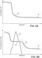
- the Figure 6A illustrates the cadmium concentration profile obtained during the first measurement.
- the ordinate is presented the concentration measured in arbitrary units and on the abscissa is presented a depth measurement in the substrate, in arbitrary units, such that an outer surface of the passivation layer 5 is considered as the origin of the abscissa.
- References to structural elements of the diode are to be read in connection with the figure 5 .
- the cadmium concentration profile 18 has a maximum plateau that seems to identify the passivation layer 5. A concentration drop corresponding to the passage in the sole 1 in Hg 1-x Cd x Te is then observable. It continues rapidly in a final cadmium plateau corresponding to the cadmium concentration in the sole 1. In the sole 1, close to the passivation layer 5, there is a slight gradient 19 of cadmium greater than the amount of cadmium present in the remainder of the sole 1. This gradient 19 is the sign of a limited diffusion of cadmium in the sole 1 since the passivation layer 5.
- the Figure 6B illustrates the concentration profiles obtained during the second measurement.
- the ordinate is presented the concentration measured in arbitrary units and on the abscissa is presented a depth measurement in the substrate, in arbitrary units, such that an outer surface of the passivation layer 5 is considered as the origin of the abscissa.
- the cadmium profile 18 'is maximum corresponds to the passivation layer 5. It is then observed, in the direction of the increasing abscissa, a first drop of the profile, then a plateau 22 of cadmium. Following the plateau 22 of cadmium, a second fall of the profile 25 is presented.
- the plate 22 defines an area corresponding to the box 12 of second cadmium concentration.
- the second drop of the cadmium profile corresponds to the intermediate zone mentioned above, comprising a cadmium concentration gradient of intermediate values between the first concentration and the second concentration.
- the cadmium profile 18 corroborates the formation of a box in Hg 1-y Cd y Te in which the value of the composition is greater than the value x representing the first concentration of cadmium in the sole 1.
- the positioning of the p / n junction 10 can be observed.
- the junction p / n according to an observation of the profiles of the Figure 6B , is located at the profile drop 25 of the cadmium profile 18 '. It is thus observable that the junction p / n is located more deeply than the box 12, in the intermediate zone identified by the concentration gradient of the second drop of the cadmium profile.
- the intermediate zone straddles a region of the n-doped sole 1 and the p + doped zone 9.
- the method and the device according to the invention make it possible to obtain diode arrays or diodes alone to manufacture, in particular, infrared imagers capable of detecting low-energy electromagnetic waves while minimizing noise and dark current and having better diode performance homogeneity.
Landscapes
- Light Receiving Elements (AREA)
- Solid State Image Pick-Up Elements (AREA)
Applications Claiming Priority (2)
| Application Number | Priority Date | Filing Date | Title |
|---|---|---|---|
| FR1103617A FR2983351B1 (fr) | 2011-11-28 | 2011-11-28 | Diode p/n a heterostructure controlee autopositionnee sur hgcdte pour imageurs infrarouges |
| PCT/EP2012/073629 WO2013079446A1 (fr) | 2011-11-28 | 2012-11-26 | DIODE P/N A HETEROSTRUCTURE CONTRÔLEE AUTOPOSITIONNEE SUR HgCdTe POUR IMAGEURS INFRAROUGES |
Publications (2)
| Publication Number | Publication Date |
|---|---|
| EP2786425A1 EP2786425A1 (fr) | 2014-10-08 |
| EP2786425B1 true EP2786425B1 (fr) | 2016-03-02 |
Family
ID=47221434
Family Applications (1)
| Application Number | Title | Priority Date | Filing Date |
|---|---|---|---|
| EP12790573.5A Active EP2786425B1 (fr) | 2011-11-28 | 2012-11-26 | Diode p/n à hétérostructure controlée autopositionnée sur hgcdte pour imageurs infrarouges |
Country Status (10)
| Country | Link |
|---|---|
| US (1) | US9178101B2 (enExample) |
| EP (1) | EP2786425B1 (enExample) |
| JP (1) | JP6151266B2 (enExample) |
| KR (1) | KR102064542B1 (enExample) |
| CN (1) | CN103959482B (enExample) |
| FR (1) | FR2983351B1 (enExample) |
| IL (1) | IL232856A (enExample) |
| IN (1) | IN2014MN00998A (enExample) |
| RU (1) | RU2618483C2 (enExample) |
| WO (1) | WO2013079446A1 (enExample) |
Families Citing this family (16)
| Publication number | Priority date | Publication date | Assignee | Title |
|---|---|---|---|---|
| FR2983351B1 (fr) | 2011-11-28 | 2014-01-24 | Commissariat Energie Atomique | Diode p/n a heterostructure controlee autopositionnee sur hgcdte pour imageurs infrarouges |
| CN103855007A (zh) * | 2012-11-30 | 2014-06-11 | 中国科学院微电子研究所 | P型mosfet的制造方法 |
| CN103855013A (zh) * | 2012-11-30 | 2014-06-11 | 中国科学院微电子研究所 | N型mosfet的制造方法 |
| FR3000609B1 (fr) | 2012-12-31 | 2015-01-30 | Commissariat Energie Atomique | Structure semiconductrice du type photodiode a avalanche a haut rapport signal sur bruit et procede de fabrication d'une telle photodiode |
| FR3020176B1 (fr) * | 2014-04-22 | 2017-09-29 | Commissariat Energie Atomique | Matrice de photodiodes en cdhgte |
| FR3021807B1 (fr) | 2014-05-27 | 2017-09-29 | Commissariat A L Energie Atomique Et Aux Energies Alternatives | Matrice de photodiodes mesa a ftm amelioree |
| FR3023976B1 (fr) | 2014-07-16 | 2017-11-17 | Commissariat Energie Atomique | Matrice de photodiodes cdhgte a faible bruit |
| FR3027452B1 (fr) * | 2014-10-21 | 2016-12-09 | Commissariat Energie Atomique | Procede de fabrication d'une photodiode a faible bruit |
| FR3042310B1 (fr) * | 2015-10-12 | 2018-10-12 | Commissariat A L'energie Atomique Et Aux Energies Alternatives | Fabrication d'une matrice de photodiodes multispectrale en cdhgte par diffusion de cadmium |
| FR3050572B1 (fr) | 2016-04-26 | 2018-04-13 | Commissariat A L'energie Atomique Et Aux Energies Alternatives | Dispositif de photo-detection a reseau inter-diodes sur-dope et procede de fabrication |
| FR3053837B1 (fr) | 2016-07-08 | 2018-08-24 | Commissariat A L'energie Atomique Et Aux Energies Alternatives | Structure du type photodiode a avalanche et procede de fabrication d'une telle structure |
| FR3089063A1 (fr) | 2018-11-27 | 2020-05-29 | Commissariat A L'energie Atomique Et Aux Energies Alternatives | Photodiode sam à multiplication d’un seul type de porteurs dans une région à multicouche périodique |
| IL297009B2 (en) * | 2020-04-09 | 2025-11-01 | Commissariat Energie Atomique | Process for manufacturing a low-noise photodetector device in a cdhgte substrate |
| FR3113781B1 (fr) | 2020-08-25 | 2022-12-16 | Commissariat Energie Atomique | PROCÉDÉ DE FABRICATION D’UN DISPOSITIF DE PHOTODÉTECTION À FAIBLE BRUIT DANS UN SUBSTRAT EN CdHgTe. |
| FR3109244B1 (fr) | 2020-04-09 | 2022-04-01 | Commissariat Energie Atomique | Dispositif de photo-détection à gradient latéral de concentration en cadmium dans la zone de charge d’espace |
| KR102672685B1 (ko) * | 2021-12-17 | 2024-06-05 | 한국과학기술연구원 | nBn구조를 이용한 중적외선 광검출소자 및 이의 제조방법 |
Family Cites Families (24)
| Publication number | Priority date | Publication date | Assignee | Title |
|---|---|---|---|---|
| US4137544A (en) * | 1977-07-05 | 1979-01-30 | Honeywell Inc. | Mercury cadmium telluride photodiode |
| JPS61256676A (ja) * | 1985-05-09 | 1986-11-14 | Mitsubishi Electric Corp | 半導体装置 |
| FR2592740B1 (fr) * | 1986-01-08 | 1988-03-18 | Commissariat Energie Atomique | Detecteur photovoltaique en hgcdte a heterojonction et son procede de fabrication |
| JPS63237484A (ja) * | 1987-03-25 | 1988-10-03 | Mitsubishi Electric Corp | 半導体装置 |
| US5936268A (en) * | 1988-03-29 | 1999-08-10 | Raytheon Company | Epitaxial passivation of group II-VI infrared photodetectors |
| US5880510A (en) * | 1988-05-11 | 1999-03-09 | Raytheon Company | Graded layer passivation of group II-VI infrared photodetectors |
| JPH03148185A (ja) * | 1989-11-02 | 1991-06-24 | Mitsubishi Electric Corp | 赤外線検知器 |
| JPH06163469A (ja) * | 1992-11-20 | 1994-06-10 | Fujitsu Ltd | 半導体のエッチング方法および該エッチング方法を用いた光検知素子の製造方法 |
| JPH06260675A (ja) * | 1993-03-09 | 1994-09-16 | Fujitsu Ltd | 光検知素子およびその製造方法 |
| US5466953A (en) * | 1993-05-28 | 1995-11-14 | Santa Barbara Research Center | Denuded zone field effect photoconductive detector |
| JPH0779008A (ja) * | 1993-06-30 | 1995-03-20 | Fujitsu Ltd | 赤外線検出装置 |
| JP2699838B2 (ja) * | 1993-11-25 | 1998-01-19 | 日本電気株式会社 | 赤外線検出器とその製造方法 |
| IL108589A (en) * | 1994-02-08 | 1998-06-15 | Technion Res & Dev Foundation | SINGLE LAYER PLANAR Hg Cd Te PHOTOVOLTAIC INFRARED DETECTOR WITH HETEROSTRUCTURE PASSIVATION AND P-ON-N HOMOJUNCTION |
| JP2001274421A (ja) * | 2000-03-23 | 2001-10-05 | Toshiba Corp | 化合物半導体素子およびその製造方法 |
| US7041983B2 (en) * | 2001-10-12 | 2006-05-09 | Lockheed Martin Corporation | Planar geometry buried junction infrared detector and focal plane array |
| RU2244365C1 (ru) * | 2003-12-09 | 2005-01-10 | Федеральное государственное унитарное предприятие "Альфа" | Фотоприемное устройство |
| FR2868602B1 (fr) | 2004-04-05 | 2006-05-26 | Commissariat Energie Atomique | Circuit de detection photonique a structure mesa |
| GB0407804D0 (en) * | 2004-04-06 | 2004-05-12 | Qinetiq Ltd | Manufacture of cadmium mercury telluride |
| US7368762B2 (en) * | 2005-01-06 | 2008-05-06 | Teledyne Licensing, Llc | Heterojunction photodiode |
| FR2934716B1 (fr) | 2008-07-31 | 2010-09-10 | Commissariat Energie Atomique | Diode electroluminescente en materiau semiconducteur et son procede de fabrication |
| US8541256B2 (en) * | 2011-04-17 | 2013-09-24 | Chang-Feng Wan | Method of cadmium molecular beam based anneals for manufacture of HgCdTe photodiode arrays |
| FR2983351B1 (fr) | 2011-11-28 | 2014-01-24 | Commissariat Energie Atomique | Diode p/n a heterostructure controlee autopositionnee sur hgcdte pour imageurs infrarouges |
| FR3000608B1 (fr) | 2012-12-31 | 2015-03-06 | Commissariat Energie Atomique | Structure semiconductrice du type photodiode a avalanche et procede de fabrication d'une telle structure |
| FR3000610B1 (fr) | 2012-12-31 | 2015-03-06 | Commissariat Energie Atomique | Structure semiconductrice du type photodiode a avalanche a faible temps de reponse et procede de fabrication d'une telle photodiode |
-
2011
- 2011-11-28 FR FR1103617A patent/FR2983351B1/fr not_active Expired - Fee Related
-
2012
- 2012-11-26 IN IN998MUN2014 patent/IN2014MN00998A/en unknown
- 2012-11-26 US US14/359,216 patent/US9178101B2/en active Active
- 2012-11-26 KR KR1020147017990A patent/KR102064542B1/ko active Active
- 2012-11-26 WO PCT/EP2012/073629 patent/WO2013079446A1/fr not_active Ceased
- 2012-11-26 RU RU2014126434A patent/RU2618483C2/ru active
- 2012-11-26 JP JP2014542878A patent/JP6151266B2/ja active Active
- 2012-11-26 EP EP12790573.5A patent/EP2786425B1/fr active Active
- 2012-11-26 CN CN201280058391.1A patent/CN103959482B/zh active Active
-
2014
- 2014-05-28 IL IL232856A patent/IL232856A/en active IP Right Grant
Also Published As
| Publication number | Publication date |
|---|---|
| IL232856A (en) | 2017-03-30 |
| CN103959482B (zh) | 2016-10-12 |
| KR102064542B1 (ko) | 2020-01-09 |
| JP6151266B2 (ja) | 2017-06-21 |
| FR2983351A1 (fr) | 2013-05-31 |
| CN103959482A (zh) | 2014-07-30 |
| IL232856A0 (en) | 2014-07-31 |
| JP2015504607A (ja) | 2015-02-12 |
| KR20140098838A (ko) | 2014-08-08 |
| WO2013079446A1 (fr) | 2013-06-06 |
| RU2014126434A (ru) | 2016-01-27 |
| US9178101B2 (en) | 2015-11-03 |
| IN2014MN00998A (enExample) | 2015-04-24 |
| FR2983351B1 (fr) | 2014-01-24 |
| RU2618483C2 (ru) | 2017-05-03 |
| US20140319580A1 (en) | 2014-10-30 |
| EP2786425A1 (fr) | 2014-10-08 |
Similar Documents
| Publication | Publication Date | Title |
|---|---|---|
| EP2786425B1 (fr) | Diode p/n à hétérostructure controlée autopositionnée sur hgcdte pour imageurs infrarouges | |
| EP0350351B1 (fr) | Photodiode et matrice de photodiodes sur matériau II-VI et leurs procédés de fabrication | |
| EP3012876B1 (fr) | Procede de fabrication d'une photodiode a faible bruit | |
| FR2872345A1 (fr) | Procede de formation d'une zone de passivation sur un dispositif semi-conducteur, reseau de photodiodes sensibles au rayonnement infrarouge, son procede de fabrication et procede de passivation d'une surface d'un corps. | |
| EP2975643B1 (fr) | Matrice de photodiodes cdhgte a faible bruit | |
| EP2339640A1 (fr) | Photodétecteur à structure plasmon | |
| EP2937902B1 (fr) | Matrice de photodiodes en cdhgte | |
| EP1903612B1 (fr) | Photodiode à avalanche | |
| EP2786426B1 (fr) | Structure semiconductrice apte a recevoir un rayonnement électromagnétique, composant semiconducteur et procédé de fabrication d'une telle structure semiconductrice | |
| EP2750203B1 (fr) | Structure semiconductrice du type photodiode à avalanche à faible temps de réponse et procédé de fabrication d'une telle photodiode | |
| EP3240030B1 (fr) | Dispositif de photo-détection à réseau inter-diodes sur-dopé et procédé de fabrication | |
| EP0913002B1 (fr) | Detecteur infrarouge bicolore a coherence spatio-temporelle planaire | |
| EP3267493A1 (fr) | Structure du type photodiode à avalanche et procédé de fabrication d'une telle structure | |
| Mollard et al. | HgCdTe FPAs made by Arsenic-ion implantation | |
| EP3381056B1 (fr) | Dispositif de photo-détection à réseau inter-diodes sur-dopé par diffusion de metal et procédé de fabrication | |
| KR20090056934A (ko) | 광 검출기 및 광 검출기의 제조 방법 | |
| EP4097766B1 (fr) | Dispositif de photo-détection à gradient latéral de concentration en cadmium dans la zone de charge d'espace | |
| EP3208854A1 (fr) | Structure de type photodiode, composant et procédé de fabrication d'une structure | |
| EP3000132A1 (fr) | Matrice de photodiode à absorption réglable de charge | |
| FR2742581A1 (fr) | Detecteur infrarouge bicolore a coherence spatio-temporelle planaire |
Legal Events
| Date | Code | Title | Description |
|---|---|---|---|
| PUAI | Public reference made under article 153(3) epc to a published international application that has entered the european phase |
Free format text: ORIGINAL CODE: 0009012 |
|
| 17P | Request for examination filed |
Effective date: 20140528 |
|
| AK | Designated contracting states |
Kind code of ref document: A1 Designated state(s): AL AT BE BG CH CY CZ DE DK EE ES FI FR GB GR HR HU IE IS IT LI LT LU LV MC MK MT NL NO PL PT RO RS SE SI SK SM TR |
|
| RIN1 | Information on inventor provided before grant (corrected) |
Inventor name: ROTHMAN,JOHAN Inventor name: BAIER, NICOLAS Inventor name: MOLLARD, LAURENT |
|
| DAX | Request for extension of the european patent (deleted) | ||
| RIN1 | Information on inventor provided before grant (corrected) |
Inventor name: ROTHMAN,JOHAN Inventor name: MOLLARD, LAURENT Inventor name: BAIER, NICOLAS |
|
| GRAP | Despatch of communication of intention to grant a patent |
Free format text: ORIGINAL CODE: EPIDOSNIGR1 |
|
| INTG | Intention to grant announced |
Effective date: 20150708 |
|
| GRAS | Grant fee paid |
Free format text: ORIGINAL CODE: EPIDOSNIGR3 |
|
| INTG | Intention to grant announced |
Effective date: 20151217 |
|
| INTG | Intention to grant announced |
Effective date: 20151215 |
|
| GRAA | (expected) grant |
Free format text: ORIGINAL CODE: 0009210 |
|
| AK | Designated contracting states |
Kind code of ref document: B1 Designated state(s): AL AT BE BG CH CY CZ DE DK EE ES FI FR GB GR HR HU IE IS IT LI LT LU LV MC MK MT NL NO PL PT RO RS SE SI SK SM TR |
|
| REG | Reference to a national code |
Ref country code: GB Ref legal event code: FG4D Free format text: NOT ENGLISH |
|
| REG | Reference to a national code |
Ref country code: AT Ref legal event code: REF Ref document number: 778546 Country of ref document: AT Kind code of ref document: T Effective date: 20160315 Ref country code: CH Ref legal event code: EP |
|
| REG | Reference to a national code |
Ref country code: IE Ref legal event code: FG4D Free format text: LANGUAGE OF EP DOCUMENT: FRENCH |
|
| REG | Reference to a national code |
Ref country code: DE Ref legal event code: R096 Ref document number: 602012015272 Country of ref document: DE |
|
| REG | Reference to a national code |
Ref country code: NL Ref legal event code: MP Effective date: 20160302 |
|
| REG | Reference to a national code |
Ref country code: LT Ref legal event code: MG4D |
|
| REG | Reference to a national code |
Ref country code: AT Ref legal event code: MK05 Ref document number: 778546 Country of ref document: AT Kind code of ref document: T Effective date: 20160302 |
|
| PG25 | Lapsed in a contracting state [announced via postgrant information from national office to epo] |
Ref country code: NO Free format text: LAPSE BECAUSE OF FAILURE TO SUBMIT A TRANSLATION OF THE DESCRIPTION OR TO PAY THE FEE WITHIN THE PRESCRIBED TIME-LIMIT Effective date: 20160602 Ref country code: GR Free format text: LAPSE BECAUSE OF FAILURE TO SUBMIT A TRANSLATION OF THE DESCRIPTION OR TO PAY THE FEE WITHIN THE PRESCRIBED TIME-LIMIT Effective date: 20160603 Ref country code: ES Free format text: LAPSE BECAUSE OF FAILURE TO SUBMIT A TRANSLATION OF THE DESCRIPTION OR TO PAY THE FEE WITHIN THE PRESCRIBED TIME-LIMIT Effective date: 20160302 Ref country code: HR Free format text: LAPSE BECAUSE OF FAILURE TO SUBMIT A TRANSLATION OF THE DESCRIPTION OR TO PAY THE FEE WITHIN THE PRESCRIBED TIME-LIMIT Effective date: 20160302 Ref country code: FI Free format text: LAPSE BECAUSE OF FAILURE TO SUBMIT A TRANSLATION OF THE DESCRIPTION OR TO PAY THE FEE WITHIN THE PRESCRIBED TIME-LIMIT Effective date: 20160302 |
|
| PG25 | Lapsed in a contracting state [announced via postgrant information from national office to epo] |
Ref country code: LV Free format text: LAPSE BECAUSE OF FAILURE TO SUBMIT A TRANSLATION OF THE DESCRIPTION OR TO PAY THE FEE WITHIN THE PRESCRIBED TIME-LIMIT Effective date: 20160302 Ref country code: NL Free format text: LAPSE BECAUSE OF FAILURE TO SUBMIT A TRANSLATION OF THE DESCRIPTION OR TO PAY THE FEE WITHIN THE PRESCRIBED TIME-LIMIT Effective date: 20160302 Ref country code: SE Free format text: LAPSE BECAUSE OF FAILURE TO SUBMIT A TRANSLATION OF THE DESCRIPTION OR TO PAY THE FEE WITHIN THE PRESCRIBED TIME-LIMIT Effective date: 20160302 Ref country code: LT Free format text: LAPSE BECAUSE OF FAILURE TO SUBMIT A TRANSLATION OF THE DESCRIPTION OR TO PAY THE FEE WITHIN THE PRESCRIBED TIME-LIMIT Effective date: 20160302 Ref country code: AT Free format text: LAPSE BECAUSE OF FAILURE TO SUBMIT A TRANSLATION OF THE DESCRIPTION OR TO PAY THE FEE WITHIN THE PRESCRIBED TIME-LIMIT Effective date: 20160302 Ref country code: PL Free format text: LAPSE BECAUSE OF FAILURE TO SUBMIT A TRANSLATION OF THE DESCRIPTION OR TO PAY THE FEE WITHIN THE PRESCRIBED TIME-LIMIT Effective date: 20160302 Ref country code: RS Free format text: LAPSE BECAUSE OF FAILURE TO SUBMIT A TRANSLATION OF THE DESCRIPTION OR TO PAY THE FEE WITHIN THE PRESCRIBED TIME-LIMIT Effective date: 20160302 |
|
| PG25 | Lapsed in a contracting state [announced via postgrant information from national office to epo] |
Ref country code: EE Free format text: LAPSE BECAUSE OF FAILURE TO SUBMIT A TRANSLATION OF THE DESCRIPTION OR TO PAY THE FEE WITHIN THE PRESCRIBED TIME-LIMIT Effective date: 20160302 Ref country code: IS Free format text: LAPSE BECAUSE OF FAILURE TO SUBMIT A TRANSLATION OF THE DESCRIPTION OR TO PAY THE FEE WITHIN THE PRESCRIBED TIME-LIMIT Effective date: 20160702 |
|
| PG25 | Lapsed in a contracting state [announced via postgrant information from national office to epo] |
Ref country code: SK Free format text: LAPSE BECAUSE OF FAILURE TO SUBMIT A TRANSLATION OF THE DESCRIPTION OR TO PAY THE FEE WITHIN THE PRESCRIBED TIME-LIMIT Effective date: 20160302 Ref country code: SM Free format text: LAPSE BECAUSE OF FAILURE TO SUBMIT A TRANSLATION OF THE DESCRIPTION OR TO PAY THE FEE WITHIN THE PRESCRIBED TIME-LIMIT Effective date: 20160302 Ref country code: RO Free format text: LAPSE BECAUSE OF FAILURE TO SUBMIT A TRANSLATION OF THE DESCRIPTION OR TO PAY THE FEE WITHIN THE PRESCRIBED TIME-LIMIT Effective date: 20160302 Ref country code: PT Free format text: LAPSE BECAUSE OF FAILURE TO SUBMIT A TRANSLATION OF THE DESCRIPTION OR TO PAY THE FEE WITHIN THE PRESCRIBED TIME-LIMIT Effective date: 20160704 Ref country code: CZ Free format text: LAPSE BECAUSE OF FAILURE TO SUBMIT A TRANSLATION OF THE DESCRIPTION OR TO PAY THE FEE WITHIN THE PRESCRIBED TIME-LIMIT Effective date: 20160302 |
|
| REG | Reference to a national code |
Ref country code: FR Ref legal event code: PLFP Year of fee payment: 5 |
|
| REG | Reference to a national code |
Ref country code: DE Ref legal event code: R097 Ref document number: 602012015272 Country of ref document: DE |
|
| PLBE | No opposition filed within time limit |
Free format text: ORIGINAL CODE: 0009261 |
|
| STAA | Information on the status of an ep patent application or granted ep patent |
Free format text: STATUS: NO OPPOSITION FILED WITHIN TIME LIMIT |
|
| PG25 | Lapsed in a contracting state [announced via postgrant information from national office to epo] |
Ref country code: DK Free format text: LAPSE BECAUSE OF FAILURE TO SUBMIT A TRANSLATION OF THE DESCRIPTION OR TO PAY THE FEE WITHIN THE PRESCRIBED TIME-LIMIT Effective date: 20160302 |
|
| 26N | No opposition filed |
Effective date: 20161205 |
|
| PG25 | Lapsed in a contracting state [announced via postgrant information from national office to epo] |
Ref country code: BE Free format text: LAPSE BECAUSE OF NON-PAYMENT OF DUE FEES Effective date: 20161130 Ref country code: SI Free format text: LAPSE BECAUSE OF FAILURE TO SUBMIT A TRANSLATION OF THE DESCRIPTION OR TO PAY THE FEE WITHIN THE PRESCRIBED TIME-LIMIT Effective date: 20160302 Ref country code: BG Free format text: LAPSE BECAUSE OF FAILURE TO SUBMIT A TRANSLATION OF THE DESCRIPTION OR TO PAY THE FEE WITHIN THE PRESCRIBED TIME-LIMIT Effective date: 20160602 |
|
| REG | Reference to a national code |
Ref country code: CH Ref legal event code: PL |
|
| PG25 | Lapsed in a contracting state [announced via postgrant information from national office to epo] |
Ref country code: LI Free format text: LAPSE BECAUSE OF NON-PAYMENT OF DUE FEES Effective date: 20161130 Ref country code: CH Free format text: LAPSE BECAUSE OF NON-PAYMENT OF DUE FEES Effective date: 20161130 |
|
| REG | Reference to a national code |
Ref country code: IE Ref legal event code: MM4A |
|
| PG25 | Lapsed in a contracting state [announced via postgrant information from national office to epo] |
Ref country code: LU Free format text: LAPSE BECAUSE OF NON-PAYMENT OF DUE FEES Effective date: 20161130 |
|
| PG25 | Lapsed in a contracting state [announced via postgrant information from national office to epo] |
Ref country code: IE Free format text: LAPSE BECAUSE OF NON-PAYMENT OF DUE FEES Effective date: 20161126 |
|
| REG | Reference to a national code |
Ref country code: FR Ref legal event code: PLFP Year of fee payment: 6 |
|
| REG | Reference to a national code |
Ref country code: BE Ref legal event code: MM Effective date: 20161130 |
|
| PG25 | Lapsed in a contracting state [announced via postgrant information from national office to epo] |
Ref country code: HU Free format text: LAPSE BECAUSE OF FAILURE TO SUBMIT A TRANSLATION OF THE DESCRIPTION OR TO PAY THE FEE WITHIN THE PRESCRIBED TIME-LIMIT; INVALID AB INITIO Effective date: 20121126 |
|
| PG25 | Lapsed in a contracting state [announced via postgrant information from national office to epo] |
Ref country code: MK Free format text: LAPSE BECAUSE OF FAILURE TO SUBMIT A TRANSLATION OF THE DESCRIPTION OR TO PAY THE FEE WITHIN THE PRESCRIBED TIME-LIMIT Effective date: 20160302 Ref country code: CY Free format text: LAPSE BECAUSE OF FAILURE TO SUBMIT A TRANSLATION OF THE DESCRIPTION OR TO PAY THE FEE WITHIN THE PRESCRIBED TIME-LIMIT Effective date: 20160302 Ref country code: MC Free format text: LAPSE BECAUSE OF FAILURE TO SUBMIT A TRANSLATION OF THE DESCRIPTION OR TO PAY THE FEE WITHIN THE PRESCRIBED TIME-LIMIT Effective date: 20160302 |
|
| PG25 | Lapsed in a contracting state [announced via postgrant information from national office to epo] |
Ref country code: MT Free format text: LAPSE BECAUSE OF FAILURE TO SUBMIT A TRANSLATION OF THE DESCRIPTION OR TO PAY THE FEE WITHIN THE PRESCRIBED TIME-LIMIT Effective date: 20160302 |
|
| PG25 | Lapsed in a contracting state [announced via postgrant information from national office to epo] |
Ref country code: TR Free format text: LAPSE BECAUSE OF FAILURE TO SUBMIT A TRANSLATION OF THE DESCRIPTION OR TO PAY THE FEE WITHIN THE PRESCRIBED TIME-LIMIT Effective date: 20160302 Ref country code: AL Free format text: LAPSE BECAUSE OF FAILURE TO SUBMIT A TRANSLATION OF THE DESCRIPTION OR TO PAY THE FEE WITHIN THE PRESCRIBED TIME-LIMIT Effective date: 20160302 |
|
| REG | Reference to a national code |
Ref country code: DE Ref legal event code: R079 Ref document number: 602012015272 Country of ref document: DE Free format text: PREVIOUS MAIN CLASS: H01L0031103000 Ipc: H10F0030221000 |
|
| PGFP | Annual fee paid to national office [announced via postgrant information from national office to epo] |
Ref country code: GB Payment date: 20241120 Year of fee payment: 13 |
|
| PGFP | Annual fee paid to national office [announced via postgrant information from national office to epo] |
Ref country code: FR Payment date: 20241121 Year of fee payment: 13 |
|
| PGFP | Annual fee paid to national office [announced via postgrant information from national office to epo] |
Ref country code: IT Payment date: 20241129 Year of fee payment: 13 |
|
| PGFP | Annual fee paid to national office [announced via postgrant information from national office to epo] |
Ref country code: DE Payment date: 20251118 Year of fee payment: 14 |