EP2752264A1 - Surface-coated cutting tool - Google Patents
Surface-coated cutting tool Download PDFInfo
- Publication number
- EP2752264A1 EP2752264A1 EP12828780.2A EP12828780A EP2752264A1 EP 2752264 A1 EP2752264 A1 EP 2752264A1 EP 12828780 A EP12828780 A EP 12828780A EP 2752264 A1 EP2752264 A1 EP 2752264A1
- Authority
- EP
- European Patent Office
- Prior art keywords
- layer
- crystal grains
- cutting tool
- lower layer
- coated cutting
- Prior art date
- Legal status (The legal status is an assumption and is not a legal conclusion. Google has not performed a legal analysis and makes no representation as to the accuracy of the status listed.)
- Granted
Links
Images

Classifications
-
- B—PERFORMING OPERATIONS; TRANSPORTING
- B23—MACHINE TOOLS; METAL-WORKING NOT OTHERWISE PROVIDED FOR
- B23B—TURNING; BORING
- B23B27/00—Tools for turning or boring machines; Tools of a similar kind in general; Accessories therefor
- B23B27/14—Cutting tools of which the bits or tips or cutting inserts are of special material
-
- C—CHEMISTRY; METALLURGY
- C23—COATING METALLIC MATERIAL; COATING MATERIAL WITH METALLIC MATERIAL; CHEMICAL SURFACE TREATMENT; DIFFUSION TREATMENT OF METALLIC MATERIAL; COATING BY VACUUM EVAPORATION, BY SPUTTERING, BY ION IMPLANTATION OR BY CHEMICAL VAPOUR DEPOSITION, IN GENERAL; INHIBITING CORROSION OF METALLIC MATERIAL OR INCRUSTATION IN GENERAL
- C23C—COATING METALLIC MATERIAL; COATING MATERIAL WITH METALLIC MATERIAL; SURFACE TREATMENT OF METALLIC MATERIAL BY DIFFUSION INTO THE SURFACE, BY CHEMICAL CONVERSION OR SUBSTITUTION; COATING BY VACUUM EVAPORATION, BY SPUTTERING, BY ION IMPLANTATION OR BY CHEMICAL VAPOUR DEPOSITION, IN GENERAL
- C23C16/00—Chemical coating by decomposition of gaseous compounds, without leaving reaction products of surface material in the coating, i.e. chemical vapour deposition [CVD] processes
- C23C16/02—Pretreatment of the material to be coated
- C23C16/0272—Deposition of sub-layers, e.g. to promote the adhesion of the main coating
-
- C—CHEMISTRY; METALLURGY
- C23—COATING METALLIC MATERIAL; COATING MATERIAL WITH METALLIC MATERIAL; CHEMICAL SURFACE TREATMENT; DIFFUSION TREATMENT OF METALLIC MATERIAL; COATING BY VACUUM EVAPORATION, BY SPUTTERING, BY ION IMPLANTATION OR BY CHEMICAL VAPOUR DEPOSITION, IN GENERAL; INHIBITING CORROSION OF METALLIC MATERIAL OR INCRUSTATION IN GENERAL
- C23C—COATING METALLIC MATERIAL; COATING MATERIAL WITH METALLIC MATERIAL; SURFACE TREATMENT OF METALLIC MATERIAL BY DIFFUSION INTO THE SURFACE, BY CHEMICAL CONVERSION OR SUBSTITUTION; COATING BY VACUUM EVAPORATION, BY SPUTTERING, BY ION IMPLANTATION OR BY CHEMICAL VAPOUR DEPOSITION, IN GENERAL
- C23C16/00—Chemical coating by decomposition of gaseous compounds, without leaving reaction products of surface material in the coating, i.e. chemical vapour deposition [CVD] processes
- C23C16/02—Pretreatment of the material to be coated
- C23C16/0272—Deposition of sub-layers, e.g. to promote the adhesion of the main coating
- C23C16/029—Graded interfaces
-
- C—CHEMISTRY; METALLURGY
- C23—COATING METALLIC MATERIAL; COATING MATERIAL WITH METALLIC MATERIAL; CHEMICAL SURFACE TREATMENT; DIFFUSION TREATMENT OF METALLIC MATERIAL; COATING BY VACUUM EVAPORATION, BY SPUTTERING, BY ION IMPLANTATION OR BY CHEMICAL VAPOUR DEPOSITION, IN GENERAL; INHIBITING CORROSION OF METALLIC MATERIAL OR INCRUSTATION IN GENERAL
- C23C—COATING METALLIC MATERIAL; COATING MATERIAL WITH METALLIC MATERIAL; SURFACE TREATMENT OF METALLIC MATERIAL BY DIFFUSION INTO THE SURFACE, BY CHEMICAL CONVERSION OR SUBSTITUTION; COATING BY VACUUM EVAPORATION, BY SPUTTERING, BY ION IMPLANTATION OR BY CHEMICAL VAPOUR DEPOSITION, IN GENERAL
- C23C16/00—Chemical coating by decomposition of gaseous compounds, without leaving reaction products of surface material in the coating, i.e. chemical vapour deposition [CVD] processes
- C23C16/22—Chemical coating by decomposition of gaseous compounds, without leaving reaction products of surface material in the coating, i.e. chemical vapour deposition [CVD] processes characterised by the deposition of inorganic material, other than metallic material
- C23C16/30—Deposition of compounds, mixtures or solid solutions, e.g. borides, carbides, nitrides
- C23C16/36—Carbonitrides
-
- C—CHEMISTRY; METALLURGY
- C23—COATING METALLIC MATERIAL; COATING MATERIAL WITH METALLIC MATERIAL; CHEMICAL SURFACE TREATMENT; DIFFUSION TREATMENT OF METALLIC MATERIAL; COATING BY VACUUM EVAPORATION, BY SPUTTERING, BY ION IMPLANTATION OR BY CHEMICAL VAPOUR DEPOSITION, IN GENERAL; INHIBITING CORROSION OF METALLIC MATERIAL OR INCRUSTATION IN GENERAL
- C23C—COATING METALLIC MATERIAL; COATING MATERIAL WITH METALLIC MATERIAL; SURFACE TREATMENT OF METALLIC MATERIAL BY DIFFUSION INTO THE SURFACE, BY CHEMICAL CONVERSION OR SUBSTITUTION; COATING BY VACUUM EVAPORATION, BY SPUTTERING, BY ION IMPLANTATION OR BY CHEMICAL VAPOUR DEPOSITION, IN GENERAL
- C23C16/00—Chemical coating by decomposition of gaseous compounds, without leaving reaction products of surface material in the coating, i.e. chemical vapour deposition [CVD] processes
- C23C16/22—Chemical coating by decomposition of gaseous compounds, without leaving reaction products of surface material in the coating, i.e. chemical vapour deposition [CVD] processes characterised by the deposition of inorganic material, other than metallic material
- C23C16/30—Deposition of compounds, mixtures or solid solutions, e.g. borides, carbides, nitrides
- C23C16/40—Oxides
- C23C16/403—Oxides of aluminium, magnesium or beryllium
-
- C—CHEMISTRY; METALLURGY
- C23—COATING METALLIC MATERIAL; COATING MATERIAL WITH METALLIC MATERIAL; CHEMICAL SURFACE TREATMENT; DIFFUSION TREATMENT OF METALLIC MATERIAL; COATING BY VACUUM EVAPORATION, BY SPUTTERING, BY ION IMPLANTATION OR BY CHEMICAL VAPOUR DEPOSITION, IN GENERAL; INHIBITING CORROSION OF METALLIC MATERIAL OR INCRUSTATION IN GENERAL
- C23C—COATING METALLIC MATERIAL; COATING MATERIAL WITH METALLIC MATERIAL; SURFACE TREATMENT OF METALLIC MATERIAL BY DIFFUSION INTO THE SURFACE, BY CHEMICAL CONVERSION OR SUBSTITUTION; COATING BY VACUUM EVAPORATION, BY SPUTTERING, BY ION IMPLANTATION OR BY CHEMICAL VAPOUR DEPOSITION, IN GENERAL
- C23C16/00—Chemical coating by decomposition of gaseous compounds, without leaving reaction products of surface material in the coating, i.e. chemical vapour deposition [CVD] processes
- C23C16/44—Chemical coating by decomposition of gaseous compounds, without leaving reaction products of surface material in the coating, i.e. chemical vapour deposition [CVD] processes characterised by the method of coating
- C23C16/455—Chemical coating by decomposition of gaseous compounds, without leaving reaction products of surface material in the coating, i.e. chemical vapour deposition [CVD] processes characterised by the method of coating characterised by the method used for introducing gases into reaction chamber or for modifying gas flows in reaction chamber
- C23C16/45523—Pulsed gas flow or change of composition over time
-
- C—CHEMISTRY; METALLURGY
- C23—COATING METALLIC MATERIAL; COATING MATERIAL WITH METALLIC MATERIAL; CHEMICAL SURFACE TREATMENT; DIFFUSION TREATMENT OF METALLIC MATERIAL; COATING BY VACUUM EVAPORATION, BY SPUTTERING, BY ION IMPLANTATION OR BY CHEMICAL VAPOUR DEPOSITION, IN GENERAL; INHIBITING CORROSION OF METALLIC MATERIAL OR INCRUSTATION IN GENERAL
- C23C—COATING METALLIC MATERIAL; COATING MATERIAL WITH METALLIC MATERIAL; SURFACE TREATMENT OF METALLIC MATERIAL BY DIFFUSION INTO THE SURFACE, BY CHEMICAL CONVERSION OR SUBSTITUTION; COATING BY VACUUM EVAPORATION, BY SPUTTERING, BY ION IMPLANTATION OR BY CHEMICAL VAPOUR DEPOSITION, IN GENERAL
- C23C28/00—Coating for obtaining at least two superposed coatings either by methods not provided for in a single one of groups C23C2/00 - C23C26/00 or by combinations of methods provided for in subclasses C23C and C25C or C25D
- C23C28/04—Coating for obtaining at least two superposed coatings either by methods not provided for in a single one of groups C23C2/00 - C23C26/00 or by combinations of methods provided for in subclasses C23C and C25C or C25D only coatings of inorganic non-metallic material
- C23C28/042—Coating for obtaining at least two superposed coatings either by methods not provided for in a single one of groups C23C2/00 - C23C26/00 or by combinations of methods provided for in subclasses C23C and C25C or C25D only coatings of inorganic non-metallic material including a refractory ceramic layer, e.g. refractory metal oxides, ZrO2, rare earth oxides
-
- C—CHEMISTRY; METALLURGY
- C23—COATING METALLIC MATERIAL; COATING MATERIAL WITH METALLIC MATERIAL; CHEMICAL SURFACE TREATMENT; DIFFUSION TREATMENT OF METALLIC MATERIAL; COATING BY VACUUM EVAPORATION, BY SPUTTERING, BY ION IMPLANTATION OR BY CHEMICAL VAPOUR DEPOSITION, IN GENERAL; INHIBITING CORROSION OF METALLIC MATERIAL OR INCRUSTATION IN GENERAL
- C23C—COATING METALLIC MATERIAL; COATING MATERIAL WITH METALLIC MATERIAL; SURFACE TREATMENT OF METALLIC MATERIAL BY DIFFUSION INTO THE SURFACE, BY CHEMICAL CONVERSION OR SUBSTITUTION; COATING BY VACUUM EVAPORATION, BY SPUTTERING, BY ION IMPLANTATION OR BY CHEMICAL VAPOUR DEPOSITION, IN GENERAL
- C23C28/00—Coating for obtaining at least two superposed coatings either by methods not provided for in a single one of groups C23C2/00 - C23C26/00 or by combinations of methods provided for in subclasses C23C and C25C or C25D
- C23C28/04—Coating for obtaining at least two superposed coatings either by methods not provided for in a single one of groups C23C2/00 - C23C26/00 or by combinations of methods provided for in subclasses C23C and C25C or C25D only coatings of inorganic non-metallic material
- C23C28/044—Coating for obtaining at least two superposed coatings either by methods not provided for in a single one of groups C23C2/00 - C23C26/00 or by combinations of methods provided for in subclasses C23C and C25C or C25D only coatings of inorganic non-metallic material coatings specially adapted for cutting tools or wear applications
-
- C—CHEMISTRY; METALLURGY
- C23—COATING METALLIC MATERIAL; COATING MATERIAL WITH METALLIC MATERIAL; CHEMICAL SURFACE TREATMENT; DIFFUSION TREATMENT OF METALLIC MATERIAL; COATING BY VACUUM EVAPORATION, BY SPUTTERING, BY ION IMPLANTATION OR BY CHEMICAL VAPOUR DEPOSITION, IN GENERAL; INHIBITING CORROSION OF METALLIC MATERIAL OR INCRUSTATION IN GENERAL
- C23C—COATING METALLIC MATERIAL; COATING MATERIAL WITH METALLIC MATERIAL; SURFACE TREATMENT OF METALLIC MATERIAL BY DIFFUSION INTO THE SURFACE, BY CHEMICAL CONVERSION OR SUBSTITUTION; COATING BY VACUUM EVAPORATION, BY SPUTTERING, BY ION IMPLANTATION OR BY CHEMICAL VAPOUR DEPOSITION, IN GENERAL
- C23C30/00—Coating with metallic material characterised only by the composition of the metallic material, i.e. not characterised by the coating process
- C23C30/005—Coating with metallic material characterised only by the composition of the metallic material, i.e. not characterised by the coating process on hard metal substrates
-
- Y—GENERAL TAGGING OF NEW TECHNOLOGICAL DEVELOPMENTS; GENERAL TAGGING OF CROSS-SECTIONAL TECHNOLOGIES SPANNING OVER SEVERAL SECTIONS OF THE IPC; TECHNICAL SUBJECTS COVERED BY FORMER USPC CROSS-REFERENCE ART COLLECTIONS [XRACs] AND DIGESTS
- Y10—TECHNICAL SUBJECTS COVERED BY FORMER USPC
- Y10T—TECHNICAL SUBJECTS COVERED BY FORMER US CLASSIFICATION
- Y10T428/00—Stock material or miscellaneous articles
- Y10T428/24—Structurally defined web or sheet [e.g., overall dimension, etc.]
- Y10T428/24942—Structurally defined web or sheet [e.g., overall dimension, etc.] including components having same physical characteristic in differing degree
- Y10T428/2495—Thickness [relative or absolute]
- Y10T428/24967—Absolute thicknesses specified
- Y10T428/24975—No layer or component greater than 5 mils thick
Definitions
- the present invention relates to a surface-coated cutting tool (hereinafter, referred to as a coated cutting tool) with excellent abrasion resistance over long-term use.
- a coated cutting tool a surface-coated cutting tool
- a hard coating layer exhibits excellent flaking resistance and chipping resistance when cutting is performed on a wide variety of steel or cast iron under a heavy cutting conditions where a high load is applied to the cutting edge cut at a high depth of cutting and a fast feed at a high speed or under intermittent cutting conditions where an intermittent and impacting load is applied to the cutting edge at a high speed.
- a coated cutting tool having a vapor-deposited hard coating layer has a body (hereinafter referred to as a cutting tool body) made of tungsten carbide-based cemented carbide (hereinafter referred to as a WC) or titanium carbonitride-based cermet (hereinafter referred to as a TiCN). It also has a vapor-deposited hard coating layer formed on the cutting tool body.
- a cutting tool body made of tungsten carbide-based cemented carbide (hereinafter referred to as a WC) or titanium carbonitride-based cermet (hereinafter referred to as a TiCN). It also has a vapor-deposited hard coating layer formed on the cutting tool body.
- the hard coating layer is constituted of (a) a lower layer that is a Ti compound layer made of one or more layers selected from a Ti carbide (hereinafter referred to as a TiC) layer, a Ti nitride (hereinafter referred to as a TiN) layer, a Ti carbonitride (hereinafter referred to as a TiCN) layer, a Ti carboxide (TiCO) layer, and Ti oxycarbonitride (TiCNO) layer, and (b) an upper layer that is an alumina layer (hereinafter referred to as a Al 2 O 3 layer) having an ⁇ -type crystal structure in a chemically-deposited state.
- a TiC Ti carbide
- TiN Ti nitride
- TiCN Ti carbonitride
- TiCO Ti carboxide
- TiCNO Ti oxycarbonitride
- the above-mentioned conventionally-known coated cutting tool exhibits excellent abrasion resistance on a variety of steel or casted iron in a continuous cutting or in an intermittent cutting.
- flaking or chipping of the coating layer is likely to occur, shortening its tool life.
- Patent Literature (PTLs) 1 and 2 are known as ways to improve the lower layer.
- the grain width of the TiCN layer of the lower layer is reduced, and the surface roughness on the surface of the hard coating layer is set to an appropriate value in order to improve its impact resistance, fracture resistance, and abrasion resistance.
- a TiCNO layer having thickness of 2 to 18 ⁇ m is formed at least as the Ti compound layer.
- the surface with the strongest X-ray diffraction peak is a (422) surface or a (311) surface.
- the oxygen content in the TiCNO layer is 0.05 to 3.02 mass%.
- the width of TiCN crystal grains is reduced in the coated cutting tool described in PTL 2. Accordingly, coarsening of crystal grains on the surface of the hard coating layer and formation of local protrusions are intended to be prevented. Moreover, improvements in the strength of the TiCNO layer itself and adhesion between the lower and upper layers are attempted.
- PTLs 3 and 4 are known as ways to improve the upper layer.
- improvements of abrasion resistance and fracture resistance are attempted by configuring the peak intensity of a (030) surface, I (030), in X-ray diffraction is stronger than the peak intensity of a (104) surface, I (104), in the Al 2 O 3 layer of the upper layer.
- the Al 2 O 3 layer consisting of the upper layer is configured to be a dual-layer structure made of a top and bottom layers.
- a inclination distribution graphs are drawn in the range of 0 to 45° in the case of the top layer and in the range of 45 to 90° in the case of the bottom layer by measuring inclinations of the normal line of a (0001) surface using an electron field emitting scanning electron microscope, the highest peak exists in the inclination classification in the range of 0 to 15° and the sum of frequency in the range corresponds to 50% or more of the total in the top layer, and the highest peak exists in the inclination classification in the range of 75 to 90° and the sum of frequency in the range corresponds to 50% or more of the total in the bottom layer.
- chipping resistance is improved in the coated cutting tool described in PTL 4.
- the inventors of the present invention conducted an intensive study in order to improve the adhesion between the lower layer made of the Ti compound layer and the upper layer made of the Al 2 O 3 layer for the sake of preventing occurrence of the anomalous damage such as flaking, chipping, and the like, and lengthening the tool life.
- the adhesion between the upper and lower layers can be improved by controlling the orientation of the Al 2 O 3 crystal grains formed directly above the most outer surface of the lower layer to reduce the density of micro-pores formed at the interface between the upper and lower layer in the coated cutting tool on which the lower made of the Ti compound layer and the upper layer made of the Al 2 O 3 layer are formed. Furthermore, the hardness and strength of the entire upper layer can be retained at a high level by controlling orientation of the Al 2 O 3 crystal grains forming the entire upper layer.
- the coated cutting tool By controlling the orientations of the Al 2 O 3 as explained above, occurrence of the anomalous damage such as flaking between the upper and lower layers, chipping, or the like, can be suppressed, even if the coated cutting tool was used for the high speed heavy cutting or the high speed intermittent cutting in which a high load and a high impact are applied to its cutting edge. Thus, the coated cutting that exhibits an excellent cutting performance over long-term use can be obtained.
- the present invention is made based on the finding described above, and has aspects shown below.
- an oxygen-containing TiCN layer is formed on the outermost surface of the lower layer of the hard coating layer, for example.
- Al 2 O 3 crystal grains oriented to a (11-20) plane in a predetermined area ratio are formed directly above the interface.
- the upper layer including Al 2 O 3 crystal grains oriented to a (0001) plane in a predetermined area ratio with respect to the entire upper layer is formed. Because of configurations described above, the orientation of the Al 2 O 3 crystal grains directly above the outermost surface layer of the lower layer and the orientation of Al 2 O 3 crystal grains in the entire upper layer are controlled.
- the ratio of numbers of crystal grains at the interface between the lower and upper layers is controlled in the coated tool of the present invention. Because of this, the adhesion strength between the lower layer and upper layers constituting the hard coating layer of the coated tool can be improved. Therefore, the coated cutting tool of the present invention shows an excellent a high-temperature strength and a high-temperature hardness to exhibit an excellent cutting performance over long-term use without occurrence of flaking or chipping of the hard coating layer even if cutting is performed under the high-speed heavy cutting condition or the high-speed intermittent cutting condition in which a high load and a high impact are applied to its cutting edge in a high-speed cutting on a variety of steel, casted iron, or the like.
- coated-cutting tools are indicated below as embodiments of the present invention. Particularly, each layer constituting the hard coating layer 4 of the coated-cutting tool 1 of the present embodiment is explained in detail.
- the Ti compound layer 3 (i.e., TiC layer, TiN layer, TiCN layer, and TiCNO layer) exists as a lower layer of the Al 2 O 3 layer 2. Due to its own high-temperature strength, the Ti compound layer 3 gives high-temperature strength to the hard coating layer 4. In addition, the Ti compound layer 3 adheres to both of the cutting tool body 5 and the Al 2 O 3 layer 2. Thus, the adherence of the hard coating layer 4 to the cutting tool body 5 is retained by the action of the Ti compound layer 3. When the total thickness of the Ti compound layer 3 is less than 3 ⁇ m, the action of the Ti compound layer 3 cannot be obtained sufficiently.
- the total thickness of the Ti compound layer 3 exceeds 20 ⁇ m, thermoplastic deformation is likely to occur in the high-speed heavy cutting or the high-speed intermittent cutting involving a high heat generation to cause uneven wear. Therefore, the total thickness of the Ti compound layer 3 is set to the range from 3 to 20 ⁇ m.
- the outermost surface layer of the lower layer 3 is formed as explained below.
- the Ti compound layer made of one or more of the TiC layer, the TiN layer, the TiCN layer, the TiCO layer, and the TiCNO layer is formed by vapor deposition using a conventional chemical vapor deposition equipment (this process can be done by vapor-depositing the TiCN layer alone). Then, for example, a TiCN layer including oxygen (hereinafter referred to as an oxygen-containing TiCn layer) is formed as the outermost surface layer by using the same conventional chemical vapor deposition equipment in a condition explained below.
- a TiCN layer including oxygen hereinafter referred to as an oxygen-containing TiCn layer
- the chemical vapor deposition is performed while CO gas is supplemented to the reaction atmosphere so that the volume % of the CO gas becomes 1 to 5 volume % with respect to the total amount of the reaction gas at the end of the vapor deposition.
- CO gas is supplemented to the reaction gas for 5 to 30 minutes before the vapor deposition end point where a predetermined thickness of the layer is obtained.
- the oxygen-containing TiCN layer containing oxygen in 0.5 to 3 atomic % within the depth region of 500 nm in its thickness direction can be formed by vapor deposition.
- the outermost surface layer of the lower layer 3 made of the oxygen-containing TiCN layer is formed in the thickness of 500 nm or more at least, for example.
- the oxygen-containing TiCN layer is configured so that oxygen of 0.5 to 3 atomic % only exists within the depth region of 500 nm in the thickness direction of the oxygen-containing TiCN layer from the interface between the oxygen-containing TiCN layer and the upper layer 2, and the depth region of the oxygen-containing TiCN layer deeper than 500 nm is free of oxygen.
- the reasons for setting the average oxygen content of the oxygen-containing TiCN layer within the depth region of 500 nm as described above are as follows.
- oxygen is included within the depth region deeper than 500nm in the depth direction of the layer, structure of the TiCN outermost surface is transformed from the columnar structure to the granular structure.
- the orientation of the Al 2 O 3 crystal grains directly above the outermost surface layer of the lower layer 3 and the distribution state of the Al 2 O 3 crystal grains oriented to the (11-20) plane become unwanted states.
- a surface-coated cutting tool in which at least a TiCNO layer (thickness is 2 to 18 ⁇ m) is formed as the Ti compound layer and includes a lower layer, is disclosed.
- oxygen content with respect to the entire TiCNO layer is set 0.05 to 3.02 % by mass.
- the width of the crystal grain is reduced: prevention of coursing of the crystal grains on the surface of the hard coating layer and formation of local protrusions; improvement in the strength of the TiCNO layer itself; and improvement in the adhesiveness to the upper layer are intended.
- the oxidation state of the outermost surface of the TiCN layer is adjusted so that the depth region of 500 nm from the interface between TiCN layer constituting the outermost surface layer of the lower layer 3 and the upper layer 2 in the thickness direction of the TiCN layer includes oxygen at 0.5 to 3 atomic % in the process before formation of the nucleus of Al 2 O 3 .
- the nucleus of ⁇ -Al 2 O 3 is formed in a condition where the grain boundary on the surface of TiCN layer and the protruded and recessed part in the crystal surface is relatively intensely oxidized in the process before formation of the nucleus of Al 2 O 3 .
- the nucleuses are formed in a dispersed state, and the crystal orientation of TiCN and the relative orientation of the Al 2 O 3 nucleuses can be controlled.
- Al 2 O 3 crystal grains oriented to the (11-20) plane can be formed on the grain boundary on the surface of TiCN layer and the protruded and recessed part in the crystal surface.
- the lower layer (TiCNO layer) having layer thickness of 2 to 18 ⁇ m disclosed in the above-mentioned PTL 2 includes oxygen within the depth region deeper than 500 nm (at least within the depth region of 2 ⁇ m or deeper) in the thickness direction, the present invention is fundamentally different from the above-described related art.
- the Ti compound layer made of one or more of the TiC layer, the TiN layer, the TiCN layer, the TiCO layer, and the TiCNO layer is formed by vapor deposition using the conventional chemical vapor deposition equipment. Then, AlCl 3 gas etching is performed on the surface of the vapor-deposited lower layer 3 in the condition described below.
- oxidation treatment is performed by the mixed gas of CO and NO in the condition described below.
- the nucleuses of Al compounds needed for formation of ⁇ -Al 2 O 3 nucleus are evenly dispersed on the outermost surface of the Ti compound layer.
- ⁇ -Al 2 O 3 nucleuses can be evenly dispersed on the outermost surface of the Ti compound layer in the pre-Al 2 O 3 nucleus formation process.
- TiCl 4 gas etching treatment is performed on the surface of the oxygen-containing TiCN layer that is formed in above-described (b) and includes oxygen at 0.5 to 3 atomic %, or on the surface of the Ti compound layer that is formed in above-described (c) and the ⁇ -Al 2 O 3 nucleuses are evenly dispersed on in the condition described below, for example.
- Al 2 O 3 crystal grains in which the Al 2 O 3 crystal grains oriented to the (11-20) plane occupy 30 to 70 area % of the measurement area, are formed directly above the outermost surface layer of the lower layer 3.
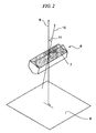
- the inclination 11 (see FIG. 2 ) of the normal line 10 of the (11-20) plane 7, which is a crystal plane of the Al 2 O 3 crystal grain 6 of the upper layer 2, to the normal line 9 of the surface of the cutting tool body can be measured in the procedure described below.
- the polished cross section perpendicular to the surface of the coated-cutting tool body of the present embodiment is prepared (see FIG 1 ).
- an electron beam is irradiated to each of the Al 2 O 3 crystal grains having the hexagonal crystal lattice existed within the measurement area with an electric field emitting scanning electron microscope to obtain data related to the orientation of the Al 2 O 3 crystal grains 6.
- the inclination 11 (see FIG 2 ) of the normal line 10 of the (11-20) plane 7, which is a crystal plane of the Al 2 O 3 crystal grain 6 of the upper layer 2, to the normal line 9 of the surface of the cutting tool body is measured. Then, based on the obtained inclinations, the area ratio of crystal grains (Al 2 O 3 crystal grains oriented to the (11-20) plane) with inclination from 0 to 10° is calculated.
- the area ratio of the formed Al 2 O 3 crystal grains oriented to the (11-20) plane obtained in above-described procedures is influenced by two factors in above-described vapor deposition condition. One is keeping the ratio of the Ar gas larger than that of H 2 gas in the TiCl 4 gas etching. Another is keeping the CO 2 gas amount larger than that of AlCl 3 gas amount in the Al 2 O 3 deposition for 5 to 30 minutes.
- the vertically elongated columnar structure of the upper layer Al 2 O 3 crystal grains 6 is formed in a lopsided state relative to the thickness direction and the fine crystal grains in the vertically elongated columnar structure are destroyed, leading to reduced adhesive strength between the upper layer Al 2 O 3 and the lower layer 3.
- the existence ratio of Al 2 O 3 crystal grains oriented to the (11-20) plane exceeds 70%
- the area ratio of the Al 2 O 3 crystal grains oriented to the (0001) plane in the upper layer Al 2 O 3 becomes less than 45 area % with respect to the whole area of the Al 2 O 3 crystal grains in the entire upper layer and the high-temperature strength of the upper layer Al 2 O 3 is reduced.
- the existence ratio of the Al 2 O 3 crystal grains oriented to the (11-20) plane is set from 30 to 70 area %.
- the Al 2 O 3 crystal grains of the upper layer are formed in the condition described below.
- the surface of the Al 2 O 3 crystal grains formed in above-described (d) (the Al 2 O 3 crystal grains in which the existence ratio of the Al 2 O 3 crystal grains oriented to (11-20) plane is set from 30 to 70 area %) is subjected to the etching treatment in the condition described below.
- the upper layer consisted of a special Al 2 O 3 layer, which is described below, can be formed.
- the special Al 2 O 3 layer is constituted from fine and vertically elongated columnar Al 2 O 3 crystal grains grown in substantially parallel to the thickness direction.
- the area ratio of the Al 2 O 3 crystal grains oriented to the (0001) plane is 45 area % or more with respect to the Al 2 O 3 crystal grains in the entire upper layer in the special Al 2 O 3 layer.
- the Al 2 O 3 crystal grains which are described in (e), grow as fine and vertically elongated columnar Al 2 O 3 crystal grains substantially parallel to the thickness direction. Furthermore, the Al 2 O 3 crystal grains oriented to the (0001) plane with respect to the Al 2 O 3 crystal grains of the entire upper layer are formed.
- the area ratio of the Al 2 O 3 crystal grains oriented to the (0001) plane is influenced particularly by the adsorption amount of AlCl 3 gas adsorbed on the surface of Al 2 O 3 by not purging the inside of the deposition equipment in Ar atmosphere after the etching treatment using AlCl 3 gas in Ar gas atmosphere.
- the area ratio of the Al 2 O 3 crystal grains oriented to the (0001) plane in the upper layer is set to 45 area % or higher, since the high-temperature hardness and high-temperature strength of the upper layer Al 2 O 3 are retained when the area ratio of the formed Al 2 O 3 crystal grains oriented to the (0001) plane is 45 area % or more.
- the area ratio of the Al 2 O 3 crystal grains oriented to the (0001) plane as described above can be obtained by following the processes explained below.
- the inclination 11 of the normal line 10 of the (0001) plane which is a crystal plane of the Al 2 O 3 crystal grain, to the normal line 9 of the surface of the cutting tool body is measured. Then, based on the obtained inclinations, the area ratio of crystal grains (Al 2 O 3 crystal grains oriented to the (0001) plane) with inclination from 0 to 10° is calculated.
- the thickness of the entire upper layer is set to 2 to 15 ⁇ m.
- the ratio value of the number of Al 2 O 3 crystal grains directly above the outermost surface layer of the lower layer 3 (it can be the oxygen-containing TiCN layer formed in above-described (b) or the Ti compound layer formed in above-described (c)) to the number of Ti compound crystal grains on the outermost surface layer of the lower layer 3 (that is (Number of Al 2 O 3 crystal grains)/(Number of Ti compound crystal grains) contacting to the interface between the upper layer 2 and the lower layer 3) is set to the range of 0.0 1 to 0.5.
- the ratio value of the number of Al 2 O 3 crystal grains contacting to the interface between the upper layer 2 and the lower layer 3 to the number of Ti compound crystal grains on the outermost surface layer of the lower layer 3 ((Number of Al 2 O 3 crystal grains)/(Number of Ti compound crystal grains)) is set to the range of 0.01 to 0.5 in the present embodiment.
- the size of the Al 2 O 3 crystal grains 6 in the vicinity of the interface is 10 nm to 50 nm.
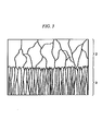
- FIG 1 The structures of the lower layer 3 and the upper layer 2 are shown in FIG 1 .
- FIG 3 The ratio of the number of crystal grains contacting to the interface between the upper layer 2 and the lower layer 3 is shown in FIG 3 .
- the WC powder, the TiC powder; the ZrC powder, the VC powder, the TaC powder, the NbC power, the Cr 3 C 2 powder, the TiN powder, and the Co powder, each of which had the average size of 1 to 3 ⁇ m were prepared.
- the above-mentioned raw material powders were mixed in the blend composition shown in Table 1.
- the mixtures were mixed in acetone with a ball mill for 24 hours.
- the mixtures were press-molded into green compacts in a predetermined shape under pressure at 98 MPa.
- the green compacts were sintered in vacuum at 5 Pa and at a predetermined temperature from 1370 to 1470°C for 1 hour.
- the cutting edge part was honed in R of 0.07mm.
- the cutting tool bodies A to F which were made of WC-base cemented carbide and had the through-away-chip-shape defined by the ISO-CNMG160608 standard, were manufactured.
- the above-mentioned raw material powders were mixed in the blend composition shown in Table 2. Then, the mixtures were mixed with a ball mill for 24 hours in wet mixing. After vacuum drying, the mixtures were press-molded into green compacts in a predetermined shape under pressure at 98 MPa. The green compacts were sintered in a nitrogen atmosphere at 1.3 KPa and at 1540°C for 1 hour.
- the cutting edge part was treated by chamfer honing of 0.1 mm of width and 20° of angle.
- the cutting tool bodies a to f which were made of TiGN-base cermet and had the chip-shape defined by the ISO-CNMG160608 standard, were manufactured.
- each of the cutting tool bodies A to F and the cutting tool bodies a to f was inserted in a conventional chemical vapor deposition equipment, and the coated cutting tools 1 to 13 of the present invention were manufactured.
- the coated cutting tools 8 to 13 were manufactured by forming the Al 2 O 3 layer of the upper layer in the intended layer thickness shown in Table 9 under the 3-steps-condition shown in Table 7 as in above-described (d).
- the comparative coated cutting tools 1 to 7 shown in Table 10 were manufactured by forming layers in the same condition for the coated cutting tools 1 to 7 of the present invention except for not performing the above-described steps (b1) and (c) for the coated cutting tools 1 to 7 of the present invention.
- the comparative coating tools 8 to 13 shown in Table 11 were manufactured. They were manufactured by forming layers in the same condition for the coated cutting tools 8 to 13 except for: allowing oxygen being included in a condition out of the above-described step (b2) for the coated cutting tools 8 to 13 of the present invention (indicated in Table 5 as "out of the scope of the present invention”); performing the TiCl 4 gas etching in a condition out of the above-described step (c) (indicated in Table 6 as "out of the scope of the present invention”); and forming the Al 2 O 3 layer in a condition out of the above-described step (d) (indicted in Table 7 as "out of the scope of the present invention”).
- a TiCN layer free of the intentionally included oxygen (hereinafter referred as "inevitable oxygen-containing TiCN layer”) was chemically vapor deposited separately on the surface of the cutting tool bodies made of tungsten carbide based cemented carbide or titanium carbonitride based cermet in the condition described below as a control.
- the inevitable oxygen-containing TiCN layer having the thickness of 3 ⁇ m or more was formed.
- the inevitably included oxygen content to the total content of Ti, C, N, and O within the depth region deeper than 100 nm from the surface of the inevitable oxygen-containing TiCN layer in the thickness direction was obtained by using an Auger electron spectroscopy Based on the measurement, the inevitable oxygen content obtained within the accuracy range of the Auger electron spectroscopy was defined as 0.5 atomic %.
- an electron beam having a diameter of 10 nm was irradiated to the polished cross section of the coated cutting tools from the surface of the outermost surface of the Ti carbonitride compound layer of the lower layer to the range of distance corresponding to the thickness of the Ti carbonitride layer in order to measure the intensities of the Auger peaks of Ti, C, N, and O.
- the Al 2 O 3 crystal grains contacting to the interface between the lower and upper layers and the TiCN crystal grains at the outermost surface layer of the lower layer were identified using an electric field emitting scanning electron microscope and an electron backscatter diffraction image system. Then, the ratio value at the interface between the lower and upper layers, (Number of Al 2 O 3 crystal grains)/(Number of Ti compound crystal grains), was obtained by measuring the numbers of the Al 2 O 3 crystal grains and the TiCN crystal grains existing within the width of 50 ⁇ m at the interface between the lower and upper layers parallel to the surface of the cutting tool body.
- the average size and the number of the micro-pores of the Al 2 O 3 crystal grains directly above the interface between the lower and upper layers of the coated cutting tools 1 to 13 of the present invention and the comparative coated cutting tools 1 to 13 were measured with a transmission electron microscope in the dark field observation of the cross section magnified by 500000-fold.
- the average size of the micro-pores existing within the range of a straight line of 50 ⁇ m in parallel with the surface of the cutting tool body was obtained as follows. First, a straight line in parallel with the surface of the cutting tool body was drawn on the micro-pores. Then, the maximum span between the intersections was calculated as the pore size. Then, pore sizes existing within the straight line of 50 ⁇ m were calculated by the method described above. Then, by calculating the average value of the sizes, the average size of the micro-pores was obtained. The number of the micro-pores was expressed as the number existing within the straight line of 50 ⁇ m.
- an area ratio of the Al 2 O 3 crystal grains oriented to the (11-20) plane was measured with an electric field emitting scanning electron microscope by following the procedure described below.
- the measurement areas of the polished cross section of the surface-coated cutting tools 1 to 13 of the present invention and the comparative coated cutting tools 1 to 13 were set in the microscope tube of the electric field emitting scanning electron microscope.
- the measurement area included the area from the interface between the lower and upper layers to 0.3 ⁇ m deep in the depth direction vertically, and within 50 ⁇ m wide in parallel with the surface of the cutting tool body horizontally (dimension: 0.3 ⁇ m ⁇ 50 ⁇ m).
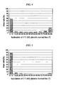
- the graph of the measurement results of the coated cutting tool 10 of the present invention is shown in FIG. 4 .
- the area ratio was obtained by: irradiating an electron beam to each of hexagonal Al 2 O 3 crystal grains of the entire upper layer within a measurement area on the polished cross section with an electric field emitting scanning electron microscope as in the case explained above; measuring inclinations of normal lines of (0001) planes of the hexagonal Al 2 O 3 crystal grains relative to a normal line of the surface of the cutting tool body; and measuring the area ratio of the crystal grains (Al 2 O 3 crystal grains oriented to the (0001) plane) having the inclinations of the normal lines of (0001) plane being 0 to 10°.
- the “entire upper layer” means a part of the measurement area ranging from the interface of the lower and upper layers to the outermost surface of the upper layer.
- the part of the measurement area corresponding to the "entire upper layer” includes the part of the measurement area where the Al 2 O 3 crystal grains oriented to the (11-20) plane exist above the interface directly.
- thicknesses of each constituting layer of the hard coating layer of the coated cutting tools 1 to 13 of the present invention and the comparative coated cutting tools 1 to 13 were measured with an electron scanning microscope (measurement in the vertical cross section). In each layer, the thickness was substantially the same average layer thickness as the intended layer thickness (the average value was obtained from 5-point measurement).
- Type Blend composition (mass %) Co TiC ZrC VC TaC NbC Cr 3 C 2 TiN WC Cutting tool body A 5.0 2 - - 5 1 0.4 1.5 Balance B 5.7 - - - 1.5 0.5 - - Balance C 6.0 - - - - - 0.3 - Balance D 8.5 - 3 - 4 - - - Balance E 10.5 3 - - 4.5 0.5 - 2.5 Balance F 12.0 4 - 0.2 - 6 0.8 - Balance [Table 2] Type Blend composition (mass %) Co Ni ZrC TaC NbC Mo 2 C WC TiCN Cutting tool body a 13 5 - 10 - 10 16 Balance b 8 7 - 5 - 7.5 - Balance C 5 - - - - 6 10 Balance d 10 5 - 11 2 - - Balance e 9 4 1 8 - 10 10 Balance f 12 5.5 - 10 - 9.5 14.5 Balance [Table 3] Lower layer (Ti compound layer)
- the crystal grain ratio indicates the value, (Number of Al 2 O 3 crystal grains)/(Number of Ti compound crystal grains). *2.
- the micro-pore distribution indicates the pore size and the number of pores per um 2 . *3.
- the TiCNO layer is distinguished from the oxygen-containing TiCN layer since the oxygen content of the TiCNO layer is around 25 atomic % as shown in Table 3 and evidently higher than that of the oxygen-containing TiCN layer.
- Type Cutting tool body symbol Hard coating layer
- Lower layer (Ti compound layer) (number in parentheses indicates intended thickness of layer in ⁇ m) Interface between lower and upper layers
- Lower layer surface treatment type Outermost surface layer of the lower layer (oxygen-containing TiCN layer) Al 2 O 3 crystal grains directly above the interface Crystal grain ratio *1
- Micro-pore Deposition type Layer thickness ( ⁇ m) Area ratio of Al 2 O 3 crystal grain oriented to the (0001) plane (area %) Forming type Layer thickness ( ⁇ m) Average oxygen content (atomic %) Etching type Deposition type Area ratio of Al 2 O 3 crystal grains oriented to the (11-20) plane (area %)
- the crystal grain ratio indicates the value, (Number of Al 2 O 3 crystal grains)/(Number of Ti compound crystal grains ⁇ . *2.
- the micro-pore distribution indicates the pore size and the number of pores per um 2 . *3. "The average oxygen content is 0 atomic %" means that only the unavoidable trace amount of oxygen is detected.
- Type Cutting tool body symbol Hard coating layer
- Lower layer (Ti compound layer) (number in parentheses indicates intended thickness of layer in ⁇ m) Interface between lower and upper layers
- Lower layer surface treatment type Outermost surface layer of the lower layer (oxygen-containing TiCN layer) Al 2 O 3 crystal grains directly above the interface Crystal grain ratio *1 Micro-poro distribution *2 Deposition type Layer thickness ( ⁇ m) Area ratio of Al 2 O 3 crystal grains oriental to the (0001) plane (area %) Forming type Layer thickness ( ⁇ m) Average oxygen content (atomic %) Etching type Deposition type Area ratio of Al 2 O 3 crystal grains oriented to the (11-20) plane (area %) The depth region deeper than 500 nm To the depth region of 500 nm 1 Same as the coated cutting tool 1 of the present invention - - - - - - - - 93 1.0 30nm 2 pores/ ⁇ m 2 A 2 3 2 Same as the coated
- the crystal grain ratio indicates the value, (Number of AlO 3 crystal grams)/(Number ofTi compound crystal grains). *2.
- the micro-pore distribution indicates the pore size and the number of pores per um 2 .
- Type Cutting tool body symbol Hard coating layer Lower layer (Ti compound layer) (number in parentheses indicates intended thickness of layer in ⁇ m) Interface between lower and upper layers Upper layer (Al 2 O 3 layer) 1st layer 2nd layer 3rd layer 4th layer Lower layer surface treatment type Outermost surface layer of the lower layer (oxygen-containing TiCN layer) Al 2 O 3 crystal grains directly above the interface Crystal ratio *1 Micro-pore distribution *2 Deposition type Layer thickness ( ⁇ m) Area ratio of Al 2 O 3 crystal grain oriented to the (0001) plane (area %) Forming type Layer thickness ( ⁇ m) Average oxygen content (atomic %) Etching type Deposition type Area ratio of Al 2 O 3 crystal grains oriented to the (11-20) plane (area %) The depth region deeper than 500 nm To the depth region of 500 n
- cutting tests were performed on the coated cutting tools 1 to 13 of the present invention and the comparative cutting tools 1 to 13.
- the coated cutting tool was fixed on the apical part of a steel tool in a screwed state with a fixation jig.
- the width of the flank wear in the cutting edge was measured.
- the ratio of the number of Al 2 O 3 crystal grains directly above the interface between the lower and upper layers to the number of the oxygen-containing TiCN crystal grains was in the range from 0.01 to 0.5 in the coated cutting tools 1 to 13 of the present invention.
- the area ratio of the Al 2 O 3 crystal grains oriented to the (11-20) plane to the Al 2 O 3 crystal grains directly above the interface between the lower and upper layers was in the range of 30 to 70 area %.
- the area ratio of the Al 2 O 3 crystal grains oriented to the (0001) plane to the Al 2 O 3 crystal grains in the entire upper layer was 45 % area % or more.
- the hard coating layer of the coated cutting tools of the present invention showed an excellent flaking resistance and an excellent chipping resistance even if they were used in the high-speed heavy cutting condition, which involves high heat generation and a high load applied on the cutting edge, or the high-speed intermittent cutting condition, which involves an intermittent and impacting load applied on the cutting edge.
- the oxygen-containing TiCN layer which is the outermost surface layer of the lower layer, includes oxygen in the oxygen content of 0.3 to 3 atomic % only in the depth region of 500 nm.
- the coated cutting tool of the present invention exhibits an excellent cutting performance for long-term use without occurrence of flaking or chipping of the hard coating layer not only in continuous or intermittent cutting of a variety of steel or casted iron under normal conditions but also under severe cutting conditions such as a high-speed heavy cutting and a high-speed intermittent cutting, in which a high, intermittent, and impacting load is applied to its cutting edge.
- it can be utilized in order to sufficiently improve the performance of the cutting apparatus.
- it can be utilized for power-saving, energy-saving, and reducing cost sufficiently
Landscapes
- Chemical & Material Sciences (AREA)
- Engineering & Computer Science (AREA)
- Mechanical Engineering (AREA)
- Chemical Kinetics & Catalysis (AREA)
- Materials Engineering (AREA)
- Metallurgy (AREA)
- Organic Chemistry (AREA)
- General Chemical & Material Sciences (AREA)
- Inorganic Chemistry (AREA)
- Ceramic Engineering (AREA)
- Chemical Vapour Deposition (AREA)
- Cutting Tools, Boring Holders, And Turrets (AREA)
Abstract
Description
- The present invention relates to a surface-coated cutting tool (hereinafter, referred to as a coated cutting tool) with excellent abrasion resistance over long-term use. In the coated cutting tool, a hard coating layer exhibits excellent flaking resistance and chipping resistance when cutting is performed on a wide variety of steel or cast iron under a heavy cutting conditions where a high load is applied to the cutting edge cut at a high depth of cutting and a fast feed at a high speed or under intermittent cutting conditions where an intermittent and impacting load is applied to the cutting edge at a high speed.
- Priority is claimed on Japanese Patent Application No.
2011-189003, filed August 31, 2011 2012-187859, filed August 28, 2012 - Conventionally, a coated cutting tool having a vapor-deposited hard coating layer is known. The conventionally-known coated cutting tool has a body (hereinafter referred to as a cutting tool body) made of tungsten carbide-based cemented carbide (hereinafter referred to as a WC) or titanium carbonitride-based cermet (hereinafter referred to as a TiCN). It also has a vapor-deposited hard coating layer formed on the cutting tool body. The hard coating layer is constituted of (a) a lower layer that is a Ti compound layer made of one or more layers selected from a Ti carbide (hereinafter referred to as a TiC) layer, a Ti nitride (hereinafter referred to as a TiN) layer, a Ti carbonitride (hereinafter referred to as a TiCN) layer, a Ti carboxide (TiCO) layer, and Ti oxycarbonitride (TiCNO) layer, and (b) an upper layer that is an alumina layer (hereinafter referred to as a Al2O3 layer) having an α-type crystal structure in a chemically-deposited state.
- The above-mentioned conventionally-known coated cutting tool exhibits excellent abrasion resistance on a variety of steel or casted iron in a continuous cutting or in an intermittent cutting. However, when it is subjected to a high-speed heavy cutting or a high-speed intermittent cutting, flaking or chipping of the coating layer is likely to occur, shortening its tool life.
- Under such circumstances, in order to suppress flaking and chipping of the coating layer, various coated cutting tools with improved lower and upper layers have been proposed.
- For example, Patent Literature (PTLs) 1 and 2 are known as ways to improve the lower layer. In the lower layer of the coated cutting tool described in
PTL 1, the grain width of the TiCN layer of the lower layer is reduced, and the surface roughness on the surface of the hard coating layer is set to an appropriate value in order to improve its impact resistance, fracture resistance, and abrasion resistance. In the lower layer of the coated cutting tool described inPTL 2, a TiCNO layer having thickness of 2 to 18 µm is formed at least as the Ti compound layer. In the TiCNO layer, the surface with the strongest X-ray diffraction peak is a (422) surface or a (311) surface. In addition, the oxygen content in the TiCNO layer is 0.05 to 3.02 mass%. In addition to the above-described configurations, the width of TiCN crystal grains is reduced in the coated cutting tool described inPTL 2. Accordingly, coarsening of crystal grains on the surface of the hard coating layer and formation of local protrusions are intended to be prevented. Moreover, improvements in the strength of the TiCNO layer itself and adhesion between the lower and upper layers are attempted. - For example,
PTLs PTL 3, improvements of abrasion resistance and fracture resistance are attempted by configuring the peak intensity of a (030) surface, I (030), in X-ray diffraction is stronger than the peak intensity of a (104) surface, I (104), in the Al2O3 layer of the upper layer. In the coated cutting tool described inPTL 4, the Al2O3 layer consisting of the upper layer is configured to be a dual-layer structure made of a top and bottom layers. Further, when a inclination distribution graphs are drawn in the range of 0 to 45° in the case of the top layer and in the range of 45 to 90° in the case of the bottom layer by measuring inclinations of the normal line of a (0001) surface using an electron field emitting scanning electron microscope, the highest peak exists in the inclination classification in the range of 0 to 15° and the sum of frequency in the range corresponds to 50% or more of the total in the top layer, and the highest peak exists in the inclination classification in the range of 75 to 90° and the sum of frequency in the range corresponds to 50% or more of the total in the bottom layer. By having the dual-layer structure configured as described above, chipping resistance is improved in the coated cutting tool described inPTL 4. -
- PTL 1: Japanese Unexamined Patent Application, First Publication No.
2007-260851 - PTL 2: Japanese Patent (Granted) Publication No.
3808648 - PTL 3: Japanese Patent (Granted) Publication No.
3291775 - PTL 4: Japanese Unexamined Patent Application, First Publication No.
2007-152491 - In recently years, the performance of the cutting machines is significantly improved. On the other hand, there is a strong demand for saving energy and reducing cost in the cutting work. In responding to the demand, the cutting work is further speeded up. At the same time, the trend is inclined to the cutting work in which a high load is applied to the cutting edge as in the heavy cutting, the intermittent cutting, or the like with a high depth of cutting or a fast feed. When the above-mentioned conventionally known coated cutting tool is used for the heavy or intermittent cutting on steels or casted iron in the normal condition, there would be no particular problem. However, when it is used for a high-speed heavy cutting or a high-speed intermittent cutting, the adhesion strength between the lower layer made of the Ti compound layer consisting of the hard coating layer, and the upper layer made of the Al2O3 layer consisting of the hard coating layer, is not sufficient. Therefore, anomalous damage, such as flaking between the upper and lower layers, chipping, and the like, occurs, the cutting tool being reached to the tool life in a relatively short period of time.
- Under the circumstance described above, the inventors of the present invention conducted an intensive study in order to improve the adhesion between the lower layer made of the Ti compound layer and the upper layer made of the Al2O3 layer for the sake of preventing occurrence of the anomalous damage such as flaking, chipping, and the like, and lengthening the tool life.
- The adhesion between the upper and lower layers can be improved by controlling the orientation of the Al2O3 crystal grains formed directly above the most outer surface of the lower layer to reduce the density of micro-pores formed at the interface between the upper and lower layer in the coated cutting tool on which the lower made of the Ti compound layer and the upper layer made of the Al2O3 layer are formed. Furthermore, the hardness and strength of the entire upper layer can be retained at a high level by controlling orientation of the Al2O3 crystal grains forming the entire upper layer. By controlling the orientations of the Al2O3 as explained above, occurrence of the anomalous damage such as flaking between the upper and lower layers, chipping, or the like, can be suppressed, even if the coated cutting tool was used for the high speed heavy cutting or the high speed intermittent cutting in which a high load and a high impact are applied to its cutting edge. Thus, the coated cutting that exhibits an excellent cutting performance over long-term use can be obtained.
- The present invention is made based on the finding described above, and has aspects shown below.
- (1) A surface-coated cutting tool including:
- a cutting tool body made of tungsten carbide-based cemented carbide or titanium carbonitride-based cermet; and
- a hard coating layer vapor-deposited on a surface of the cutting tool body, wherein
- the hard coating layer includes a lower layer formed on the surface of the cutting tool body and an upper layer formed on the lower layer,
- (a) the lower layer is a Ti compound layer, which is consists of one or more layers selected from the group consisting of a Ti carbide layer, a Ti nitride layer, a Ti carbonitride layer, a Ti carboxide layer, and a Ti oxycarbonitride layer, with a total average thickness of 3 to 20 µm,
- (b) the upper layer is an Al2O3 layer, which has an α-type crystal structure in a chemically vapor-deposited state, with an average thickness of 2 to 15 µm,
- (c) in a case of:
- preparing a polished cross section of the surface-coated cutting tool perpendicular to the surface of the cutting tool body;
- irradiating an electron beam to each of hexagonal Al2O3 crystal grains of the upper layer contacting to an interface between an outermost surface layer of the lower layer and the upper layer within a measurement area on the polished cross section with an electric field emitting scanning electron microscope; and
- measuring inclinations of normal lines of (11-20) planes of the hexagonal Al2O3 crystal grains relative to a normal line of the surface of the cutting tool body,
- (d) in a case of:
- irradiating an electron beam to each of hexagonal Al2O3 crystal grains of the entire upper layer within a measurement area on the polished cross section with an electric field emitting scanning electron microscope; and
- measuring inclinations of normal lines of (0001) planes of the hexagonal Al2O3 crystal grains relative to a normal line of the surface of the cutting tool body,
- (2) The surface-coated cutting tool according to (1) described above, wherein the outermost surface layer of the lower layer is made of the Ti carbonitride layer having a thickness of 500 nm or more,
oxygen is only included within a depth region of 500 nm of the Ti carbonitride layer in the thickness direction from an interface between the Ti carbonitride layer and the upper layer, and
an average oxygen content within the depth region is 0.5 to 3 atomic % with respect to a total atomic content of Ti, C, N, and O included within the depth region. - (3) The surface-coated cutting tool according to (2) described above, wherein a ratio of the number of Al2O3 crystal grains directly above the outermost surface layer of the lower layer to the number of crystal grains of the Ti carbonitride layer in the outermost surface layer of the lower layer is 0.01 to 0.5 at the interface between the Ti carbonitride layer, which constitutes the outermost surface layer of the lower layer, and the upper layer.
- In the coated tool, which is an aspect of the present invention (hereinafter referred to as a coated tool of the present invention), an oxygen-containing TiCN layer is formed on the outermost surface of the lower layer of the hard coating layer, for example. Also, Al2O3 crystal grains oriented to a (11-20) plane in a predetermined area ratio are formed directly above the interface. Also, the upper layer including Al2O3 crystal grains oriented to a (0001) plane in a predetermined area ratio with respect to the entire upper layer is formed. Because of configurations described above, the orientation of the Al2O3 crystal grains directly above the outermost surface layer of the lower layer and the orientation of Al2O3 crystal grains in the entire upper layer are controlled. More preferably, the ratio of numbers of crystal grains at the interface between the lower and upper layers is controlled in the coated tool of the present invention. Because of this, the adhesion strength between the lower layer and upper layers constituting the hard coating layer of the coated tool can be improved. Therefore, the coated cutting tool of the present invention shows an excellent a high-temperature strength and a high-temperature hardness to exhibit an excellent cutting performance over long-term use without occurrence of flaking or chipping of the hard coating layer even if cutting is performed under the high-speed heavy cutting condition or the high-speed intermittent cutting condition in which a high load and a high impact are applied to its cutting edge in a high-speed cutting on a variety of steel, casted iron, or the like.
-
-
FIG 1 is a schematic view of the cross-section perpendicular to the surface of the cutting tool body in the surface-coated cutting tool of an embodiment of the present invention. -
FIG 2 is a perspective view showing the inclination of the normal line of a (11-20) plane, which is a crystal plane of Al2O3 crystal grain of the upper layer, to the normal line of the surface of the cutting tool body in the surface-coated cutting tool of an embodiment of the present invention. -
FIG 3 is a schematic view of the interface between the upper and lower layers in the surface-coated cutting tool of an embodiment of the present invention. -
FIG 4 is a frequency distribution graph of a inclination of the normal line of a (11-20) plane, which is a crystal plane of Al2O3 crystal grain of the upper layer, to the normal line of the surface of the cutting tool body in the surface-coated cutting tool of an embodiment of the present invention. -
FIG 5 is a graph of measurement results of the area ratio of thecoated cutting tool 10 of the present invention. - Explanations about coated-cutting tools are indicated below as embodiments of the present invention. Particularly, each layer constituting the
hard coating layer 4 of the coated-cuttingtool 1 of the present embodiment is explained in detail. - Basically, the Ti compound layer 3 (i.e., TiC layer, TiN layer, TiCN layer, and TiCNO layer) exists as a lower layer of the Al2O3 layer 2. Due to its own high-temperature strength, the
Ti compound layer 3 gives high-temperature strength to thehard coating layer 4. In addition, theTi compound layer 3 adheres to both of thecutting tool body 5 and the Al2O3 layer 2. Thus, the adherence of thehard coating layer 4 to thecutting tool body 5 is retained by the action of theTi compound layer 3. When the total thickness of theTi compound layer 3 is less than 3 µm, the action of theTi compound layer 3 cannot be obtained sufficiently. On the other hand, when the total thickness of theTi compound layer 3 exceeds 20 µm, thermoplastic deformation is likely to occur in the high-speed heavy cutting or the high-speed intermittent cutting involving a high heat generation to cause uneven wear. Therefore, the total thickness of theTi compound layer 3 is set to the range from 3 to 20 µm. - For example, the outermost surface layer of the
lower layer 3 is formed as explained below. - First, the Ti compound layer made of one or more of the TiC layer, the TiN layer, the TiCN layer, the TiCO layer, and the TiCNO layer is formed by vapor deposition using a conventional chemical vapor deposition equipment (this process can be done by vapor-depositing the TiCN layer alone). Then, for example, a TiCN layer including oxygen (hereinafter referred to as an oxygen-containing TiCn layer) is formed as the outermost surface layer by using the same conventional chemical vapor deposition equipment in a condition explained below.
- Composition of reaction gas (volume %): 3 to 8% of TiCl4; 1.0 to 2.0% of CH3CN; 40 to 60% of N2; and balance H2
- Temperature of reaction atmosphere: 750 to 900°C
- Pressure of reaction atmosphere: 6 to 10 kPa
- In this occasion, the chemical vapor deposition is performed while CO gas is supplemented to the reaction atmosphere so that the volume % of the CO gas becomes 1 to 5 volume % with respect to the total amount of the reaction gas at the end of the vapor deposition. CO gas is supplemented to the reaction gas for 5 to 30 minutes before the vapor deposition end point where a predetermined thickness of the layer is obtained. By following the procedures, the oxygen-containing TiCN layer containing oxygen in 0.5 to 3 atomic % within the depth region of 500 nm in its thickness direction can be formed by vapor deposition.
- In order to form a suitable Al2O3 crystal grains on the outermost surface layer (see (d) explained later), preferably the outermost surface layer of the
lower layer 3 made of the oxygen-containing TiCN layer is formed in the thickness of 500 nm or more at least, for example. At the same time, preferably the oxygen-containing TiCN layer is configured so that oxygen of 0.5 to 3 atomic % only exists within the depth region of 500 nm in the thickness direction of the oxygen-containing TiCN layer from the interface between the oxygen-containing TiCN layer and theupper layer 2, and the depth region of the oxygen-containing TiCN layer deeper than 500 nm is free of oxygen. - The reasons for setting the average oxygen content of the oxygen-containing TiCN layer within the depth region of 500 nm as described above are as follows. When oxygen is included within the depth region deeper than 500nm in the depth direction of the layer, structure of the TiCN outermost surface is transformed from the columnar structure to the granular structure. Furthermore, the orientation of the Al2O3 crystal grains directly above the outermost surface layer of the
lower layer 3 and the distribution state of the Al2O3 crystal grains oriented to the (11-20) plane become unwanted states. - When the average oxygen content within the depth region of 500 nm is less than 0.5 atomic %, adhesion strength between the
upper layer 2 and the lower TiCN layer cannot be improved. At the same time, the orientation of the Al2O3 crystal grains directly above the outermost surface layer of thelower layer 3 and the distribution state of the Al2O3 crystal grains oriented to the (11-20) plane cannot be satisfied. On the other hand, when the average oxygen content within this depth region exceeds 3 atomic %, on the upper layer Al2O3 directly above the interface, the area ratio occupied by Al2O3 crystal grains oriented to the (0001) plane ("Al2O3 crystal grains oriented to the (0001) plane" will be explained later) becomes less than 45 area % with respect to the entire area of Al2O3 in the entire upper layer, and the high-temperature strength of theupper layer 2 is reduced. - The average oxygen concentration means the oxygen (O) content in the total content of titanium (Ti), carbon (C), nitrogen (N), and oxygen (O) represented in atomic % within the depth region of 500 nm in the thickness direction of the TiCN layer from the interface between the TiCN layer constituting the outermost surface layer of the
lower layer 3 and the upper layer 2 (=O/(Ti+C+N+O)×100). - In
PTL 2 referred as a related art, a surface-coated cutting tool, in which at least a TiCNO layer (thickness is 2 to 18 µm) is formed as the Ti compound layer and includes a lower layer, is disclosed. In the lower layer of the surface-coated cutting tool disclosed inPTL 2, oxygen content with respect to the entire TiCNO layer is set 0.05 to 3.02 % by mass. In this related art, the width of the crystal grain is reduced: prevention of coursing of the crystal grains on the surface of the hard coating layer and formation of local protrusions; improvement in the strength of the TiCNO layer itself; and improvement in the adhesiveness to the upper layer are intended. However, there is no modification on the orientation of the upper layer. - In the present embodiment, the oxidation state of the outermost surface of the TiCN layer is adjusted so that the depth region of 500 nm from the interface between TiCN layer constituting the outermost surface layer of the
lower layer 3 and theupper layer 2 in the thickness direction of the TiCN layer includes oxygen at 0.5 to 3 atomic % in the process before formation of the nucleus of Al2O3. In other words, the nucleus of α-Al2O3 is formed in a condition where the grain boundary on the surface of TiCN layer and the protruded and recessed part in the crystal surface is relatively intensely oxidized in the process before formation of the nucleus of Al2O3. By varying the oxidation state of the outermost surface of the TiCN layer before the Al2O3 nucleus formation process, the nucleuses are formed in a dispersed state, and the crystal orientation of TiCN and the relative orientation of the Al2O3 nucleuses can be controlled. Thus, Al2O3 crystal grains oriented to the (11-20) plane can be formed on the grain boundary on the surface of TiCN layer and the protruded and recessed part in the crystal surface. - Since the lower layer (TiCNO layer) having layer thickness of 2 to 18 µm disclosed in the above-mentioned
PTL 2 includes oxygen within the depth region deeper than 500 nm (at least within the depth region of 2 µm or deeper) in the thickness direction, the present invention is fundamentally different from the above-described related art. - (c) The above-described (b) forms the oxygen-containing TiCN layer as the outermost surface layer of the
lower layer 3. However, the outermost surface layer with different configurations can be formed as explained below. - As in above-described (b), first, the Ti compound layer made of one or more of the TiC layer, the TiN layer, the TiCN layer, the TiCO layer, and the TiCNO layer is formed by vapor deposition using the conventional chemical vapor deposition equipment. Then, AlCl3 gas etching is performed on the surface of the vapor-deposited
lower layer 3 in the condition described below. - Composition of reaction gas (volume %): 0.1 to 1% of AlCl3; and balance H2
- Temperature of reaction atmosphere: 750 to 900°C
- Pressure of the reaction atmosphere: 6 to 10 kPa
- Time: 1 to 5 minutes
- Then, oxidation treatment is performed by the mixed gas of CO and NO in the condition described below.
- Composition of reaction gas (volume %): 5 to 10% of CO; 5 to 10% of NO; and balance H2
- Temperature of reaction atmosphere: 750 to 900°C
- Pressure of the reaction atmosphere: 6 to 10 kPa
- Time: 1 to 5 minutes
- By following the above-described processes, the nucleuses of Al compounds needed for formation of α-Al2O3 nucleus are evenly dispersed on the outermost surface of the Ti compound layer. Thus,α-Al2O3 nucleuses can be evenly dispersed on the outermost surface of the Ti compound layer in the pre-Al2O3 nucleus formation process.
- TiCl4 gas etching treatment is performed on the surface of the oxygen-containing TiCN layer that is formed in above-described (b) and includes oxygen at 0.5 to 3 atomic %, or on the surface of the Ti compound layer that is formed in above-described (c) and the α-Al2O3 nucleuses are evenly dispersed on in the condition described below, for example.
- Composition of reaction gas (volume %): 1 to 5% of TiCl4; 10 to 30% of H2; and balance Ar
- Temperature of reaction atmosphere: 750 to 900°C
- Pressure of the reaction atmosphere: 6 to 10 kPa
- Then, after the internal atmosphere being purged by making Ar atmosphere in the equipment, setting temperature at 750 to 900°C, pressure at 6 to 10 KPa, Al2O3 deposition is performed in the condition described below.
- Composition of reaction gas (volume %): 1 to 3% of
AlCl 3 10 to 30% of CO2; and balance H2 - Temperature of reaction atmosphere: 960 to 1040°C
- Pressure of the reaction atmosphere: 6 to 10 kPa
- Time: 5 to 30 minutes
- By following the above-described processes, Al2O3 crystal grains, in which the Al2O3 crystal grains oriented to the (11-20) plane occupy 30 to 70 area % of the measurement area, are formed directly above the outermost surface layer of the
lower layer 3. - The inclination 11 (see
FIG. 2 ) of thenormal line 10 of the (11-20)plane 7, which is a crystal plane of the Al2O3 crystal grain 6 of theupper layer 2, to thenormal line 9 of the surface of the cutting tool body can be measured in the procedure described below. - First, the polished cross section perpendicular to the surface of the coated-cutting tool body of the present embodiment is prepared (see
FIG 1 ). Next, by setting the above-described (d) Al2O3 crystal grains formed directly above the outermost surface layer of the lower layer 3 (directly above the interface between the upper and lower layers) to be the measuring objects, an electron beam is irradiated to each of the Al2O3 crystal grains having the hexagonal crystal lattice existed within the measurement area with an electric field emitting scanning electron microscope to obtain data related to the orientation of the Al2O3 crystal grains 6. Then, based on the data, the inclination 11 (seeFIG 2 ) of thenormal line 10 of the (11-20)plane 7, which is a crystal plane of the Al2O3 crystal grain 6 of theupper layer 2, to thenormal line 9 of the surface of the cutting tool body is measured. Then, based on the obtained inclinations, the area ratio of crystal grains (Al2O3 crystal grains oriented to the (11-20) plane) with inclination from 0 to 10° is calculated. - The area ratio of the formed Al2O3 crystal grains oriented to the (11-20) plane obtained in above-described procedures is influenced by two factors in above-described vapor deposition condition. One is keeping the ratio of the Ar gas larger than that of H2 gas in the TiCl4 gas etching. Another is keeping the CO2 gas amount larger than that of AlCl3 gas amount in the Al2O3 deposition for 5 to 30 minutes. When the Al2O3 crystal grains oriented to the (11-20) plane is less than 30 area % of the measurement area, the vertically elongated columnar structure of the upper layer Al2O3 crystal grains 6 is formed in a lopsided state relative to the thickness direction and the fine crystal grains in the vertically elongated columnar structure are destroyed, leading to reduced adhesive strength between the upper layer Al2O3 and the
lower layer 3. On the other hand, when the existence ratio of Al2O3 crystal grains oriented to the (11-20) plane exceeds 70%, the area ratio of the Al2O3 crystal grains oriented to the (0001) plane in the upper layer Al2O3 (explained later) becomes less than 45 area % with respect to the whole area of the Al2O3 crystal grains in the entire upper layer and the high-temperature strength of the upper layer Al2O3 is reduced. - Because of the reasons described above, in terms of the Al2O3 crystal grains directly above the interface between the
upper layer 2 and thelower layer 3, the existence ratio of the Al2O3 crystal grains oriented to the (11-20) plane is set from 30 to 70 area %. - After forming the above-described (d) Al2O3 crystal grain directly above the outermost surface layer of the
lower layer 3 by vapor deposition, the Al2O3 crystal grains of the upper layer are formed in the condition described below. - First, the surface of the Al2O3 crystal grains formed in above-described (d) (the Al2O3 crystal grains in which the existence ratio of the Al2O3 crystal grains oriented to (11-20) plane is set from 30 to 70 area %) is subjected to the etching treatment in the condition described below.
- Composition of reaction gas (volume %): 1 to 5% of Aids; and balance Ar
- Temperature of reaction atmosphere: 960 to 1040°C
- Pressure of the reaction atmosphere: 6 to 10 kPa
- Time: 1 to 5 minutes
- Then, vapor deposition is performed in the condition described below.
- Composition of reaction gas (volume %): 1 to 5% of AlCl3; 5 to 15% of CO2; 1 to 5% of HCl; 0.5 to 1% of H2S; and balance H2
- Temperature of reaction atmosphere: 960 to 1040°C
- Pressure of the reaction atmosphere: 6 to 10 kPa
- Time: Until the intended layer thickness is obtained
- By following the above-described processes, the upper layer consisted of a special Al2O3 layer, which is described below, can be formed. The special Al2O3 layer is constituted from fine and vertically elongated columnar Al2O3 crystal grains grown in substantially parallel to the thickness direction. In addition, the area ratio of the Al2O3 crystal grains oriented to the (0001) plane is 45 area % or more with respect to the Al2O3 crystal grains in the entire upper layer in the special Al2O3 layer.
- The Al2O3 crystal grains, which are described in (e), grow as fine and vertically elongated columnar Al2O3 crystal grains substantially parallel to the thickness direction. Furthermore, the Al2O3 crystal grains oriented to the (0001) plane with respect to the Al2O3 crystal grains of the entire upper layer are formed. The area ratio of the Al2O3 crystal grains oriented to the (0001) plane is influenced particularly by the adsorption amount of AlCl3 gas adsorbed on the surface of Al2O3 by not purging the inside of the deposition equipment in Ar atmosphere after the etching treatment using AlCl3 gas in Ar gas atmosphere.
- In the present invention, the area ratio of the Al2O3 crystal grains oriented to the (0001) plane in the upper layer is set to 45 area % or higher, since the high-temperature hardness and high-temperature strength of the upper layer Al2O3 are retained when the area ratio of the formed Al2O3 crystal grains oriented to the (0001) plane is 45 area % or more.
- The area ratio of the Al2O3 crystal grains oriented to the (0001) plane as described above can be obtained by following the processes explained below. First, a polished cross section of the surface-coatad cutting tool perpendicular to the surface of the
cutting tool body 5 of the present embodiment is prepared. Next, by setting the Al2O3 crystal grains of the entire upper layer to be the measuring objects, an electron beam is irradiated to each of the Al2O3 crystal grains having the hexagonal crystal lattice existed within the measurement area with an electric field emitting scanning electron microscope to obtain data related to the orientation of the Al2O3 crystal grains. Then, based on the data, theinclination 11 of thenormal line 10 of the (0001) plane, which is a crystal plane of the Al2O3 crystal grain, to thenormal line 9 of the surface of the cutting tool body is measured. Then, based on the obtained inclinations, the area ratio of crystal grains (Al2O3 crystal grains oriented to the (0001) plane) with inclination from 0 to 10° is calculated. - When the thickness of the entire upper layer is less than 2 µm, it cannot exhibit the excellent high-temperature strength and the high-temperature hardness for long-term use. On the other hand, when it exceeds 15 µm, chipping is likely to occur. Therefore, the thickness of the upper layer is set to 2 to 15 µm.
- In the present embodiment, the ratio value of the number of Al2O3 crystal grains directly above the outermost surface layer of the lower layer 3 (it can be the oxygen-containing TiCN layer formed in above-described (b) or the Ti compound layer formed in above-described (c)) to the number of Ti compound crystal grains on the outermost surface layer of the lower layer 3 (that is (Number of Al2O3 crystal grains)/(Number of Ti compound crystal grains) contacting to the interface between the
upper layer 2 and the lower layer 3) is set to the range of 0.0 1 to 0.5. When this value is less than 0.01; the size of the Al2O3 crystal grains becomes relatively too small leading to a reduced associativity of the Ti compound crystal grains onto the protrusions and recesses on the crystal surfaces at the interface. Consequently, the adhesive strength of Al2O3 of theupper layer 2 and thelower layer 3 is reduced, and pores are likely to be formed. On the other hand, when the value exceeds 0.5, the size of Al2O3 crystal grains becomes relatively too large leading to pore-formation during Al2O3 formation in the upper layer. Consequently, the hardness and strength of Al2O3 of the upper layer are reduced, and the adhesive strength to the Ti compound of the lower layer is reduced. - Because of the reasons described above, the ratio value of the number of Al2O3 crystal grains contacting to the interface between the
upper layer 2 and thelower layer 3 to the number of Ti compound crystal grains on the outermost surface layer of the lower layer 3 ((Number of Al2O3 crystal grains)/(Number of Ti compound crystal grains)) is set to the range of 0.01 to 0.5 in the present embodiment. - Preferably, the size of the Al2O3 crystal grains 6 in the vicinity of the interface is 10 nm to 50 nm.
- The structures of the
lower layer 3 and theupper layer 2 are shown inFIG 1 . The ratio of the number of crystal grains contacting to the interface between theupper layer 2 and thelower layer 3 is shown inFIG 3 . - Next, the coated cutting tool of the present invention is specifically explained by Examples.
- As raw material powders, the WC powder, the TiC powder; the ZrC powder, the VC powder, the TaC powder, the NbC power, the Cr3C2 powder, the TiN powder, and the Co powder, each of which had the average size of 1 to 3 µm, were prepared. The above-mentioned raw material powders were mixed in the blend composition shown in Table 1. Then, after adding wax, the mixtures were mixed in acetone with a ball mill for 24 hours. After vacuum drying, the mixtures were press-molded into green compacts in a predetermined shape under pressure at 98 MPa. The green compacts were sintered in vacuum at 5 Pa and at a predetermined temperature from 1370 to 1470°C for 1 hour. After sintering, the cutting edge part was honed in R of 0.07mm. By following the above-described steps, the cutting tool bodies A to F, which were made of WC-base cemented carbide and had the through-away-chip-shape defined by the ISO-CNMG160608 standard, were manufactured.
- Also, as raw material powders, the TiCN powder (TiC/TiN=50/50 in mass ratio), the Mo2C powders, the ZrC powder, the NbC powder, the TaC powder, the WC powder, the Co powder, and the Ni powder, each of which had the average size of 0.5 to 2 µm, were prepared. The above-mentioned raw material powders were mixed in the blend composition shown in Table 2. Then, the mixtures were mixed with a ball mill for 24 hours in wet mixing. After vacuum drying, the mixtures were press-molded into green compacts in a predetermined shape under pressure at 98 MPa. The green compacts were sintered in a nitrogen atmosphere at 1.3 KPa and at 1540°C for 1 hour. After sintering, the cutting edge part was treated by chamfer honing of 0.1 mm of width and 20° of angle. By following the above-described steps, the cutting tool bodies a to f, which were made of TiGN-base cermet and had the chip-shape defined by the ISO-CNMG160608 standard, were manufactured.
- Then, each of the cutting tool bodies A to F and the cutting tool bodies a to f was inserted in a conventional chemical vapor deposition equipment, and the
coated cutting tools 1 to 13 of the present invention were manufactured. - (a) First, the Ti compound layers having the intended layer thickness shown in Tables 8 and 9 were vapor deposited under the conditions shown in Table 3 ("I-TiCN" in Table 3 indicates the condition for forming TiCN layer with the vertically grown crystal structure described in
JP-A-H06-8010 - (b1) Then, AlCl3 gas etching and oxidation treatment by the mixed gas of CO and NO were performed on the outermost surface of the Ti compound layer of the lower layer under the condition shown in Table 4.
- (c) Then, the surface of the Ti compound layer treated in above-described (b1) was treated by TiCl4 gas etching treatment under the condition shown in Table 6. Then, the inside of the equipment was purged by Ar gas.
- (d) Then, the
coated cutting tools 1 to 7 were manufactured by forming the Al2O3 layer of the upper layer in the intended layer thickness shown in Table 8 under the 3-steps-condition shown in Table 7. - (b2) The oxygen-containing TiCN layer (the TiCN layer in which oxygen is only included within the depth region of 500 nm from the surface of the layer at 0.5 to 3 atomic % (O/(Ti+PC+N+O)×100)) was formed as the outermost surface layer of the lower layer in the intended thickness shown in Table 9 under the condition shown in Table 5.
- Then, the surface of the oxygen-containing TiCN layer formed in above-described (b2) was treated by TiCl4 gas etching treatment under the condition shown in Table 6 as in above-described (c). Then, the inside of the equipment was purged by Ar gas.
- Then, the
coated cutting tools 8 to 13 were manufactured by forming the Al2O3 layer of the upper layer in the intended layer thickness shown in Table 9 under the 3-steps-condition shown in Table 7 as in above-described (d). - For the comparison purpose, the comparative
coated cutting tools 1 to 7 shown in Table 10 were manufactured by forming layers in the same condition for thecoated cutting tools 1 to 7 of the present invention except for not performing the above-described steps (b1) and (c) for thecoated cutting tools 1 to 7 of the present invention. - In addition, for the comparison purpose, the
comparative coating tools 8 to 13 shown in Table 11 were manufactured. They were manufactured by forming layers in the same condition for thecoated cutting tools 8 to 13 except for: allowing oxygen being included in a condition out of the above-described step (b2) for thecoated cutting tools 8 to 13 of the present invention (indicated in Table 5 as "out of the scope of the present invention"); performing the TiCl4 gas etching in a condition out of the above-described step (c) (indicated in Table 6 as "out of the scope of the present invention"); and forming the Al2O3 layer in a condition out of the above-described step (d) (indicted in Table 7 as "out of the scope of the present invention"). - In order to obtain oxygen contents intentionally included in the Ti carbonitride compound layer, a TiCN layer free of the intentionally included oxygen (hereinafter referred as "inevitable oxygen-containing TiCN layer") was chemically vapor deposited separately on the surface of the cutting tool bodies made of tungsten carbide based cemented carbide or titanium carbonitride based cermet in the condition described below as a control.
- Reaction gas composition (volume %): 3 to 8 % of TiCl4; 1.0 to 2.0 % of CH3CN; 40 to 60 % of N2; and balance H2
- Temperature of reaction atmosphere: 750 to 900°C
- Pressure of reaction atmosphere: 6 to 10 kPa
- By the vapor deposition described above, the inevitable oxygen-containing TiCN layer having the thickness of 3 µm or more was formed. The inevitably included oxygen content to the total content of Ti, C, N, and O within the depth region deeper than 100 nm from the surface of the inevitable oxygen-containing TiCN layer in the thickness direction was obtained by using an Auger electron spectroscopy Based on the measurement, the inevitable oxygen content obtained within the accuracy range of the Auger electron spectroscopy was defined as 0.5 atomic %.
- Next, on the
coated cutting tools 8 to 13 of the present invention and the comparativecoated cutting tools 8 to 13, the average oxygen content (=O/(Ti+C+N+O)×100) within the depth region of 500 nm in the thickness direction of the TiCN layer and the average oxygen content (=O/(Ti+C+N+O)×100) within the depth region deeper than 500 nm were measured as follows. First, an electron beam having a diameter of 10 nm was irradiated to the polished cross section of the coated cutting tools from the surface of the outermost surface of the Ti carbonitride compound layer of the lower layer to the range of distance corresponding to the thickness of the Ti carbonitride layer in order to measure the intensities of the Auger peaks of Ti, C, N, and O. Then, the ratio of the intensity of the Auger peak corresponding to O was calculated from the sum of the peak intensities. Finally, the amount of the inevitable oxygen content was subtracted from the calculated value to obtain the oxygen content of the TiCN layer. The values obtained as described above are shown in Tables 9 and 11. - Also, on the
coated cutting tools 1 to 13 of the present invention and the comparativecoated cutting tools 1 to 13, the Al2O3 crystal grains contacting to the interface between the lower and upper layers and the TiCN crystal grains at the outermost surface layer of the lower layer were identified using an electric field emitting scanning electron microscope and an electron backscatter diffraction image system. Then, the ratio value at the interface between the lower and upper layers, (Number of Al2O3 crystal grains)/(Number of Ti compound crystal grains), was obtained by measuring the numbers of the Al2O3 crystal grains and the TiCN crystal grains existing within the width of 50 µm at the interface between the lower and upper layers parallel to the surface of the cutting tool body. - More specifically, the identification of Al2O3 crystal grains at the interface between the lower and upper layers and the TiCN crystal grains of the outermost surface of the lower layer were performed as described below.
- In the case of identification of the Al2O3 crystal grains, an electron beam was irradiated to each of hexagonal Al2O3 crystal grains of the aluminum oxide upper layer within a measurement area on the polished cross section with an electric field emitting scanning electron microscope and an electron backscatter diffraction image system, and the inclinations of the normal lines of the (0001) planes and the (10-10) planes, which were crystal planes of the above-mentioned crystal grains, to the normal line of the surface of the cutting tool body were measured. Then, based on the obtained inclinations, angles of intersections between the normal lines of the (0001) planes of the adjacent crystal grains at the intersection were calculated. Also, angles of intersections between the normal lines of the (10-10) planes of the adjacent crystal grains were calculated in the same way. Then, when the angles of the intersections were 2° or more, the adjacent crystal grains were identified as two individual crystal grains.
- In the case of identification of the TiCN crystal grains, an electron beam was irradiated to each of the crystal grains of the outermost surface layer of the Ti compound layer within a measurement area on the polished cross section with an electric field emitting scanning electron microscope, and the inclinations of the normal lines of the
- (001) planes and the (011) planes, which were crystal planes of the above-mentioned crystal grains, to the normal line of the surface of the cutting tool body were measured. Then, based on the obtained inclinations, angles of intersections between the normal lines of the (001) planes of the adjacent crystal grains at the intersection were calculated. Also, angles of intersections between the normal lines of the (011) planes of the adjacent crystal grains were calculated in the same way. Then, when the angles of the intersections were 2° or more, the adjacent crystal grains were identified as two individual crystal grains.
- These values are shown in Tables 8 and 11.
- Furthermore, the average size and the number of the micro-pores of the Al2O3 crystal grains directly above the interface between the lower and upper layers of the
coated cutting tools 1 to 13 of the present invention and the comparativecoated cutting tools 1 to 13 were measured with a transmission electron microscope in the dark field observation of the cross section magnified by 500000-fold. The average size of the micro-pores existing within the range of a straight line of 50 µm in parallel with the surface of the cutting tool body was obtained as follows. First, a straight line in parallel with the surface of the cutting tool body was drawn on the micro-pores. Then, the maximum span between the intersections was calculated as the pore size. Then, pore sizes existing within the straight line of 50 µm were calculated by the method described above. Then, by calculating the average value of the sizes, the average size of the micro-pores was obtained. The number of the micro-pores was expressed as the number existing within the straight line of 50 µm. - These values are shown in Tables 8 and 11.
- In addition, in regard with the Al2O3 crystal grains directly above the interface between the lower and upper layers of the hard coating layer, an area ratio of the Al2O3 crystal grains oriented to the (11-20) plane was measured with an electric field emitting scanning electron microscope by following the procedure described below.
- First, the measurement areas of the polished cross section of the surface-coated
cutting tools 1 to 13 of the present invention and the comparativecoated cutting tools 1 to 13 were set in the microscope tube of the electric field emitting scanning electron microscope. The measurement area included the area from the interface between the lower and upper layers to 0.3 µm deep in the depth direction vertically, and within 50 µm wide in parallel with the surface of the cutting tool body horizontally (dimension: 0.3 µm×50 µm). Next, inclinations of normal lines of (11-20) planes of the hexagonal Al2O3 crystal grains relative to a normal line of the surface of the cutting tool body were measured within the measurement area of 0.3 µm×50 µm at an interval of 0.1 µm/step with an electron backscatter diffraction image system by irradiating an electron beam to each of hexagonal Al2O3 crystal grains existing within the measurement area of the polished cross section. The acceleration voltage for the electron beam was 15kV. The incident angle of the electron beam was 70°. The irradiation current for the electron beam was 1 nA. Based on these measurements, the area ratio of crystal grains (Al2O3 crystal grains oriented to the (11-20) plane) having the inclinations of the normal lines of (11-20) planes being 0 to 10° was measured. - These values are shown in Tables 8 and 11.
- The graph of the measurement results of the
coated cutting tool 10 of the present invention is shown inFIG. 4 . - In addition, in regard with the are ratio of Al2O3 crystal grains oriented to the (0001) plane in the entire upper layer of the hard coating layer of the
coated cutting tools 1 to 13 of the present invention and the comparativecoated cutting tools 1 to 13, the area ratio was obtained by: irradiating an electron beam to each of hexagonal Al2O3 crystal grains of the entire upper layer within a measurement area on the polished cross section with an electric field emitting scanning electron microscope as in the case explained above; measuring inclinations of normal lines of (0001) planes of the hexagonal Al2O3 crystal grains relative to a normal line of the surface of the cutting tool body; and measuring the area ratio of the crystal grains (Al2O3 crystal grains oriented to the (0001) plane) having the inclinations of the normal lines of (0001) plane being 0 to 10°. - The "entire upper layer" means a part of the measurement area ranging from the interface of the lower and upper layers to the outermost surface of the upper layer. Thus, the part of the measurement area corresponding to the "entire upper layer" includes the part of the measurement area where the Al2O3 crystal grains oriented to the (11-20) plane exist above the interface directly. These values are shown in Tables 8 and 11.
- Also, thicknesses of each constituting layer of the hard coating layer of the
coated cutting tools 1 to 13 of the present invention and the comparativecoated cutting tools 1 to 13 were measured with an electron scanning microscope (measurement in the vertical cross section). In each layer, the thickness was substantially the same average layer thickness as the intended layer thickness (the average value was obtained from 5-point measurement).[Table 1] Type Blend composition (mass %) Co TiC ZrC VC TaC NbC Cr3C2 TiN WC Cutting tool body A 5.0 2 - - 5 1 0.4 1.5 Balance B 5.7 - - - 1.5 0.5 - - Balance C 6.0 - - - - - 0.3 - Balance D 8.5 - 3 - 4 - - - Balance E 10.5 3 - - 4.5 0.5 - 2.5 Balance F 12.0 4 - 0.2 - 6 0.8 - Balance [Table 2] Type Blend composition (mass %) Co Ni ZrC TaC NbC Mo2C WC TiCN Cutting tool body a 13 5 - 10 - 10 16 Balance b 8 7 - 5 - 7.5 - Balance C 5 - - - - 6 10 Balance d 10 5 - 11 2 - - Balance e 9 4 1 8 - 10 10 Balance f 12 5.5 - 10 - 9.5 14.5 Balance [Table 3] Lower layer (Ti compound layer) Formation condition (pressure and temperature in reaction atmosphere are shown as kPa and °C, respectively) Type Intended composition (Numbers indicate atomic ratio) Reaction gas composition (volume %) Reaction atmosphere Pressure Temperature TiC layer TiC TiCl4: 4.2%, CH4: 8.5%, H2: balance 7 1020 TiN layer (first layer) TiN TiCl4: 4.2%, N2: 30%, H2: balance 30 900 TiN layer (other than the first layer) TiN TiCl4: 4.2%, N2: 35%, H2: balance 50 1040 I-TiCN layer TiC0.5N0.5 TiCl4: 4.2%, N2: 20%, CH3CN: 0.6%, H2: balance 7 880 TiCN layer TiC0.5N0.5 TiCl4: 4.2%, N2: 20%, CH4: 4%, H2: balance 12 1000 TiCO layer TiC0.500.5 TiCl4: 4.2%, CO: 4%, H2: balance 7 1020 TiCNO layer TiC0.2No0.3O0.5 TiCl4: 4.2%, CO: 4%, CH4: 3%, N2: 20%, H2: balance 20 1020 [Table 4] Lower layer surface treatment type Treatment condition (pressure and temperature in reaction atmosphere are shown as kPa and °C, respectively) Reaction gas composition (volume %) Reaction atmosphere Treatment time (min) Pressure Temperature A AlCl3 gas etching AlCl3: 0.1%, H2: balance 8 900 5 CO+NO mixed gas oxidation treatment CO: 10%, NO: 5%, H2: balance 8 900 1 B AlCl3 gas etching AlCl3 0.5%, H2: balance 10 800 2 CO+NO mixed gas oxidation treatment CO: 5%, NO: 5%, H2: balance 10 800 2 C AlCl3 gas etching AlCl3: 1%, H2: balance 6 750 1 CO+NO mixed gas oxidation treatment CO: 5%, NO: 10%, H2: balance 6 750 5 [Table 5] Oxygen-containing TiCN layer type Formation condition (pressure and temperature in reaction atmosphere are shown as kPa and °C, respectively) CO gas supplied 5 to 30 minutes before the end of deposition time (volume %) Reaction gas composition (volume %) Reaction atmosphere Pressure Temperature A TiCl4: 3%, CH3CN: 2%, N2: 40%, H2: balance 8 900 5 B TiCl4: 5%, CH3CN: 1%, N2: 50%, H2: balance 6 870 3 C TiCl4: 8%, CH3CN: 1.5%, N2: 60%, H2: balance 10 750 1 D (out of the scope of the present invention) TiCl4: 2.5%, CH3CN: 1.2%, N2: 35%, CO2: 2.5%, CO: 2.5%, H2: balance 8 800 - [Table 6] TiCl4 gas etching type Etching condition (pressure and temperature in reaction atmosphere are shown as kPa and °C, respectively) Reaction gas composition (volume %) Pressure Temperature A TiCl4: 1%, H2: 20%, balance: Ar 6 900 B TiCl4: 3%, H2: 30%, balance: Ar 8 800 C TiCl4: 5%, H2: 10%, balance: Ar 10 750 D (out of the scope of the present invention) TiCl4: 5%, H2: balance 6 1000 E (out of the scope of the present invention) TiCl4: 5%, balance: Ar 8 1020 [Table 7] Al2O3 layer type Deposition condition (pressure, temperature, and time are shown as kPa, °C, and minutes, respectively) Reaction gas composition (volume %) Pressure Temperature Time A 1st step AlCl3: 1%, CO2: 10%, balance: H2 6 960 5 2nd step AlCl3: 5%, balance: Ar 6 960 5 3rd step AlCl3: 1%, CO2: 5%, HCl: 1%, H2S: 0.5%, balance H2 6 960 - B 1st step AlCl3: 3%, CO2: 20%, balance: H2 8 1000 30 2nd step AlCl3 3%, balance: Ar 8 1000 3 3rd step AlCl3: 3%, CO2: 7%, HCl: 2%, H2S: 0.8%, balance H2 8 1000 - C 1st step AlCl3: 2%, CO2: 30%, balance: H2 10 1040 15 2nd step AlCl3: 1%, balance: Ar 10 1040 1 3rd step AlCl3: 5%, CO2: 15%, HCl: 5%, H2S: 1%, balance H2 10 1040 - D (out of the scope of the present invention) AlCl3: 2%, CO2: 5%, HCl: 2%; H2S: 0.2%, balance H2 6 1020 - [Table 8] Type Cutting tool body symbol Hard coating layer Lower layer (Ti compound layer)(number in parentheses indicates intended thickness of layer in µm) Interface between lower and upper layers Upper layer (Al2O3 layer) 1st layer 2nd layer 3rd layer 4th layer Lower layer surface treatment type Outermost surface layer of the lower layer (oxygen-containing TiCN layer) Al2O3 crystal gnms directly above the interface Crystal grain ratio *1 Micro-pore distribution *2 Type Layer thickness (µm) Area ratio of Al2O3 crystal grains oriented (0001) plane (area %) Type Layer thickness (µm) Average oxygen content (atomic %) Etching type Type Area ratio of Al2O3 crystal grains oriented to the (11-20) plane (area %) The depth region deeper than 500 nm To the region of 500 nm 1 A TiC (0.1) I-TiCN (2.7) TiCO (0.2) - B - - - - A B 70 0.5 No micro-pore A 2 45 2 a TiN (0.3) I-TiCN (7.0) TiCNO (0.7) *3 - C - - - - B A 66 0.3 No micro-pores B 7.5 99 3 B TiCN (0.2) I-TiCN (5) - - A - - - - C C 57 0.1 No micro-pores C 5 65 Coated cutting tools of the present invention 4 b TiN (0.2) I-TiCN (6.8) TiCN (0.3) - C - - - - B A 46 0.2 No micro-pores B 15 92 5 C TiH (0.5) I-TiCN (11) - - B - - - - C B 55 0.4 No micro-pores C 10.5 87 6 c TiN (0.5) TiC (1.0) I-TiCN (17.5) TiCO (1.0) A - - - - B C 30 0.3 No micro-pores B 12 70 7 D TiN (1) I-TiCN (14) TiCNO (0.3) TiCO (0.2) B - - - - A A 45 0.5 No micro-pores A 6.5 50 *1. The crystal grain ratio indicates the value, (Number of Al2O3 crystal grains)/(Number of Ti compound crystal grains).
*2. The micro-pore distribution indicates the pore size and the number of pores per um2.
*3. The TiCNO layer is distinguished from the oxygen-containing TiCN layer since the oxygen content of the TiCNO layer is around 25 atomic % as shown in Table 3 and evidently higher than that of the oxygen-containing TiCN layer.[Table 9] Type Cutting tool body symbol Hard coating layer Lower layer (Ti compound layer) (number in parentheses indicates intended thickness of layer in µm) Interface between lower and upper layers Upper layer (Al2O3 layer) 1st layer 2nd layer 3rd layer 4th layer Lower layer surface treatment type Outermost surface layer of the lower layer (oxygen-containing TiCN layer) Al2O3 crystal grains directly above the interface Crystal grain ratio *1 Micro-pore Deposition type Layer thickness (µm) Area ratio of Al2O3 crystal grain oriented to the (0001) plane (area %) Forming type Layer thickness (µm) Average oxygen content (atomic %) Etching type Deposition type Area ratio of Al2O3 crystal grains oriented to the (11-20) plane (area %) The deeper than 500 nm To the depth region of 500 nm 8 d TiC (0.1) - - - - B 2.9 0 1.8 A B 70 0.06 No micro-pores A 2 48 *3 9 E TiN (0.3) - - - - A 6.7 0 3 B A 66 0.05 No micro-pores B 7.5 95 *3 10 e TiN (0.1) - - - - C 14.5 0 0.5 C C 57 0.07 No micro-pores C 5 88 Conted cuting tools of the present invention *3 11 F TiN (0.2) I-TiCN (6.8) - - - A 1.5 0 3 B A 46 0.01 No micro-pores B 1.5 97 *3 12 D TiN (0.5) I-TiCN (11) - - - B 5 0 1.8 C B 55 0.04 No micro-pores C 10.5 83 *3 13 f TiN (0.5) I-TiCN - - - C 2 0 0.5 B C 32 0.02 No micro-pores B 12 95 *3 *1. The crystal grain ratio indicates the value, (Number of Al2O3 crystal grains)/(Number of Ti compound crystal grains}.
*2. The micro-pore distribution indicates the pore size and the number of pores per um2.
*3. "The average oxygen content is 0 atomic %" means that only the unavoidable trace amount of oxygen is detected.[Table 10] Type Cutting tool body symbol Hard coating layer Lower layer (Ti compound layer) (number in parentheses indicates intended thickness of layer in µm) Interface between lower and upper layers Upper layer (Al2O3 layer) 1st layer 2nd layer 3rd layer 4th layer Lower layer surface treatment type Outermost surface layer of the lower layer (oxygen-containing TiCN layer) Al2O3 crystal grains directly above the interface Crystal grain ratio *1 Micro-poro distribution *2 Deposition type Layer thickness (µm) Area ratio of Al2O3 crystal grains oriental to the (0001) plane (area %) Forming type Layer thickness (µm) Average oxygen content (atomic %) Etching type Deposition type Area ratio of Al2O3 crystal grains oriented to the (11-20) plane (area %) The depth region deeper than 500 nm To the depth region of 500 nm 1 Same as the coated cutting tool 1 of the present invention - - - - - - - 93 1.0 30nm 2 pores/µm2 A 2 3 2 Same as the coated cutting tool of the present invention - - - - - - - 1 1.5 20nm 3 pores/µm3 B 7.5 2 3 Same as the coated cutting tool 3 of the present invention - - - - - - - 7 2 50nm 2 pores/µm2 C 5 0 Comparative coated cutting tools 4 Same as the coated cutting tool 4 of the present invention - - - - - - - 2 2.5 50nm 2 pores/µm2 B 1.5 8 5 Same as the coated cutting tool 5 of the present invention - - - - - - - 10 2.2 2.5nm 3 pores/µm2 C 10.5 6 6 Same as the coated cutting tool 6 of the present invention - - - - - - - 0 1.2 20nm 3 pores/µm2 B 12 3 7 Same as the coated cutting tool 7 of the present invention - - - - - - - 89 0.9 20nm 4 pores/µm2 A 6.5 2 *1. The crystal grain ratio indicates the value, (Number of AlO3 crystal grams)/(Number ofTi compound crystal grains).
*2. The micro-pore distribution indicates the pore size and the number of pores per um2.[Table 11] Type Cutting tool body symbol Hard coating layer Lower layer (Ti compound layer) (number in parentheses indicates intended thickness of layer in µm) Interface between lower and upper layers Upper layer (Al2O3 layer) 1st layer 2nd layer 3rd layer 4th layer Lower layer surface treatment type Outermost surface layer of the lower layer (oxygen-containing TiCN layer) Al2O3 crystal grains directly above the interface Crystal ratio *1 Micro-pore distribution *2 Deposition type Layer thickness (µm) Area ratio of Al2O3 crystal grain oriented to the (0001) plane (area %) Forming type Layer thickness (µm) Average oxygen content (atomic %) Etching type Deposition type Area ratio of Al2O3 crystal grains oriented to the (11-20) plane (area %) The depth region deeper than 500 nm To the depth region of 500 nm 8 Same as the coated cutting tool 8 of the present invention - D 2 1.8 1.9 D D 0 1.5 30nmm 3 pores/µm2 D 2 0 9 Same as the coated cutting tool 9 of the present invention - D 7 1.9 2 E D 1 1.7 20nm 4 pores/µm2 D 7.5 1 10 Same as the coated tool 10 of the present invention - D 15 2 2.2 D D 2 2.2 50nm 2pores/µm2 D 5 2 Comparative coated cutting tools 11 Same as the coated cutting tool 11 of the present invention - D 18 1.9 2.1 D D 0 2.3 50nm 2 pores/µm2 D 1.5 0 12 Same as the coated cutting tool 12 of the present invention - D 6 1.8 1.9 E D 1 2.1 25nm 3 pores/µm2 D 10.5 1 13 Same as the coated cutting tool 13 of the present invention - D 3 1.7 1.8 E D 2 1.4 20nm 3 pores/µm2 D 12 0 *1. The crystal grain ratio indicates the value, (Number of Al2O3 crystal grains)/(Number of Ti compound crystal grains).
*2. The micro-pore distribution indicates the pore size and the number of pores per µm2. - Next, cutting tests were performed on the
coated cutting tools 1 to 13 of the present invention and thecomparative cutting tools 1 to 13. In each of cutting tests, the coated cutting tool was fixed on the apical part of a steel tool in a screwed state with a fixation jig. In each of cutting tests, the width of the flank wear in the cutting edge was measured. - In the cutting condition A, a dry high-speed and intermittent cutting test on a nickel-chromium-molybdenum alloy steel was performed in the condition described below (the normal cutting speed is 300 m/min).
- Work: JIS·S45C with 4 grooves with an equal interval along with the longitudinal direction
- Cutting speed: 350 m/min
- Cutting depth: 2 mm
- Feed: 0.4 mm/rev
- Cutting time: 5 minutes
- In the cutting condition B, a dry high-speed and heavy cutting test on a nickel-chromium-molybdenum alloy steel was performed in the condition described below (the normal cutting speed and the cutting depth are 250 m/lmin and 2 mm/rev, respectively).
- Work: Round bar of JIS·SNCM439
- Cutting speed: 370 m/min
- Cutting depth: 3.5 mm
- Feed: 0.25 mm/rev
- Cutting time: 8 minutes
- In the cutting condition C, a dry high-speed and high-cutting-depth cutting test on a ductile iron steel was performed in the condition described below (the normal cutting speed and the cutting depth are 250 m/min and 1.5 mm/rev, respectively).
- Work: Round bar of JIS·FCD700
- Cutting speed: 320 m/min
- Cutting depth: 2.5 mm
- Feed: 0.2 mm/rev
- Cutting time: 5 minutes
- The measurement results were indicated in Table 12.
[Table 12] Type Width of flank wear (mm) Type Cutting test result (min) Cutting condition (A) Cutting condition (B) Cutting condition (C) Cutting condition (A) Cutting condition (B) Cutting condition (C) cutting of the present invention 1 0.33 0.32 0.33 Comparative coated cutting tools 1 0.5* 1.0* 1.2* 2 0.23 0.23 0.24 2 2.2** 2.5* 2.5** 3 0.24 0.25 0.25 3 1.0* 0.5* 0.5* 4 0.31 0.30 0.32 4 0.5** 1.2** 1.5** 5 0.30 0.31 0.33 5 3.2* 2.0* 1.8** 6 0.27 0.28 0.26 6 1.4** 1.5** 0.5** 7 0.25 0.24 0.23 7 1.8* 2.8* 2.2* 8 0.23 0.22 0.24 8 1.6* 1.5** 2.4* 9 0.13 0.14 0.15 9 1.2* 0.5* 1.8** 10 0.14 0.13 0.14 10 2.8* 1.4* 0.7** 11 0.18 0.17 0.16 11 2.5** 1.3** 1.1** 12 0.17 0.18 0.18 12 0.8* 1.3* 3.1** 13 0.18 0.19 0.19 13 0.6** 0.9** 2.6** * The value indicates the cutting time until reaching to its service life by flaking occurring in the hard-coating layer
** The value indicates the cutting time until reaching to its service life by chipping occurring in the hard-coating layer - The results indicated in Tables 8, 9, and 12 demonstrate followings. First, the ratio of the number of Al2O3 crystal grains directly above the interface between the lower and upper layers to the number of the oxygen-containing TiCN crystal grains was in the range from 0.01 to 0.5 in the
coated cutting tools 1 to 13 of the present invention. Also, the area ratio of the Al2O3 crystal grains oriented to the (11-20) plane to the Al2O3 crystal grains directly above the interface between the lower and upper layers was in the range of 30 to 70 area %. Furthermore, the area ratio of the Al2O3 crystal grains oriented to the (0001) plane to the Al2O3 crystal grains in the entire upper layer was 45 % area % or more. In thecoated cutting tools 1 to 13 of the present invention, there was less micro-pores formed in the upper layer, and the sizes of the micro-pores were small. Therefore, the hard coating layer of the coated cutting tools of the present invention showed an excellent flaking resistance and an excellent chipping resistance even if they were used in the high-speed heavy cutting condition, which involves high heat generation and a high load applied on the cutting edge, or the high-speed intermittent cutting condition, which involves an intermittent and impacting load applied on the cutting edge. - In any of the
coated cutting tools 8 to 13 of the present invention, the oxygen-containing TiCN layer, which is the outermost surface layer of the lower layer, includes oxygen in the oxygen content of 0.3 to 3 atomic % only in the depth region of 500 nm. - Contrary to that, in the comparative
coated cutting tools 1 to 13, it was obvious that they reached to their tool life in a short period of time because of flaking or chipping occurred in their hard coating layer in the high-speed heavy cutting machining or the high-speed intermittent cutting machining. - As explained above, the coated cutting tool of the present invention exhibits an excellent cutting performance for long-term use without occurrence of flaking or chipping of the hard coating layer not only in continuous or intermittent cutting of a variety of steel or casted iron under normal conditions but also under severe cutting conditions such as a high-speed heavy cutting and a high-speed intermittent cutting, in which a high, intermittent, and impacting load is applied to its cutting edge. Thus, it can be utilized in order to sufficiently improve the performance of the cutting apparatus. Also, it can be utilized for power-saving, energy-saving, and reducing cost sufficiently
-
- 1: Coated cutting tool
- 2: Upper layer (Al2O3 layer)
- 3: Lower layer (Ti compound layer)
- 4: Hard coating layer
- 5: Cutting tool body
- 6: Hexagonal Al2O3 crystal grain
- 7: ((11-20) plane of hexagonal Al2O3 crystal grain
- 8: Surface of the cutting tool body
- 9: Normal line of the surface of the cutting tool body
- 10: Normal line of (11-20) plane of hexagonal Al2O3 crystal grain
- 11: Inclination of the normal line of (11-20) plane to the normal line of the surface of the cutting tool body
Claims (3)
- A surface-coated cutting tool comprising:a cutting tool body made of tungsten carbide-based cemented carbide or titanium carbonitride-based cermet; anda hard coating layer vapor-deposited on a surface of the cutting tool body, whereinthe hard coating layer comprises a lower layer formed on the surface of the cutting tool body and an upper layer formed on the lower layer,(a) the lower layer is a Ti compound layer, which is consists of one or more layers selected from the group consisting of a Ti carbide layer, a Ti nitride layer, a Ti carbonitride layer, a Ti carboxide layer, and a Ti oxycarbonitride layer, with a total average thickness of 3 to 20 µm,(b) the upper layer is an Al2O3 layer, which has an α-type crystal structure in a chemically vapor-deposited state, with an average thickness of 2 to 15 µm,(c) in a case of:preparing a polished cross section of the surface-coated cutting tool perpendicular to the surface of the cutting tool body;irradiating an electron beam to each of hexagonal Al2O3 crystal grains of the upper layer contacting to an interface between an outermost surface layer of the lower layer and the upper layer within a measurement area on the polished cross section with an electric field emitting scanning electron microscope; andmeasuring inclinations of normal lines of (11-20) planes of the hexagonal Al2O3 crystal grains relative to a normal line of the surface of the cutting tool body,an area ratio occupied by hexagonal Al2O3 crystal grains having the inclinations of the normal lines of (11-20) planes being 0 to 10° is in a range of 30 to 70 area%,(d) in a case of:irradiating an electron beam to each of hexagonal Al2O3 crystal grains of the entire upper layer within a measurement area on the polished cross section with an electric field emitting scanning electron microscope; andmeasuring inclinations of normal lines of (0001) planes of the hexagonal Al2O3 crystal grains relative to a normal line of the surface of the cutting tool body,an area ratio occupied by hexagonal Al2O3 crystal grains having the inclinations of the normal lines of (0001) plane being 0 to 10° is 45 area% or more.
- The surface-coated cutting tool according to Claim 1, wherein
the outermost surface layer of the lower layer is made of the Ti carbonitride layer having a thickness of 500 nm or more,
oxygen is only included within a depth region of 500 nm of the Ti carbonitride layer in the thickness direction from an interface between the Ti carbonitride layer and the upper layer, and
an average oxygen content within the depth region is 0.5 to 3 atomic % with respect to a total atomic content of Ti, C, N, and O included within the depth region. - The surface-coated cutting tool according to Claim 2, wherein a ratio of the number of Al2O3 crystal grains directly above the outermost surface layer of the lower layer to the number of crystal grains of the Ti carbonitride layer in the outermost surface layer of the lower layer is 0.01 to 0.5 at the interface between the Ti carbonitride layer, which constitutes the outermost surface layer of the lower layer, and the upper layer.
Applications Claiming Priority (3)
| Application Number | Priority Date | Filing Date | Title |
|---|---|---|---|
| JP2011189003 | 2011-08-31 | ||
| JP2012187859A JP5257535B2 (en) | 2011-08-31 | 2012-08-28 | Surface coated cutting tool |
| PCT/JP2012/072168 WO2013031952A1 (en) | 2011-08-31 | 2012-08-31 | Surface-coated cutting tool |
Publications (3)
| Publication Number | Publication Date |
|---|---|
| EP2752264A1 true EP2752264A1 (en) | 2014-07-09 |
| EP2752264A4 EP2752264A4 (en) | 2015-09-30 |
| EP2752264B1 EP2752264B1 (en) | 2018-07-18 |
Family
ID=47756427
Family Applications (1)
| Application Number | Title | Priority Date | Filing Date |
|---|---|---|---|
| EP12828780.2A Active EP2752264B1 (en) | 2011-08-31 | 2012-08-31 | Surface-coated cutting tool |
Country Status (6)
| Country | Link |
|---|---|
| US (1) | US9636748B2 (en) |
| EP (1) | EP2752264B1 (en) |
| JP (1) | JP5257535B2 (en) |
| KR (1) | KR20140063666A (en) |
| CN (1) | CN103764323B (en) |
| WO (1) | WO2013031952A1 (en) |
Cited By (2)
| Publication number | Priority date | Publication date | Assignee | Title |
|---|---|---|---|---|
| EP3144085A4 (en) * | 2014-05-16 | 2017-12-06 | Mitsubishi Materials Corporation | Surface coating cutting tool |
| EP3964310A4 (en) * | 2020-04-10 | 2022-05-11 | Sumitomo Electric Hardmetal Corp. | CUTTING TOOL |
Families Citing this family (26)
| Publication number | Priority date | Publication date | Assignee | Title |
|---|---|---|---|---|
| JP5838789B2 (en) * | 2011-12-22 | 2016-01-06 | 三菱マテリアル株式会社 | Surface coated cutting tool whose hard coating layer exhibits excellent chipping resistance in high-speed intermittent cutting |
| JP5994623B2 (en) * | 2012-12-20 | 2016-09-21 | 三菱マテリアル株式会社 | Surface-coated cutting tool that exhibits excellent chipping resistance and wear resistance with a hard coating layer in high-speed intermittent cutting |
| RU2667187C2 (en) | 2013-06-27 | 2018-09-17 | Сандвик Интеллекчуал Проперти Аб | Coated cutting tools |
| JP6198137B2 (en) * | 2013-12-24 | 2017-09-20 | 三菱マテリアル株式会社 | Surface coated cutting tool |
| JP6414800B2 (en) | 2014-02-26 | 2018-10-31 | 三菱マテリアル株式会社 | Surface-coated titanium carbonitride-based cermet cutting tool with excellent chipping resistance |
| JP6548072B2 (en) * | 2014-05-30 | 2019-07-24 | 三菱マテリアル株式会社 | Surface coated cutting tool |
| JP6620482B2 (en) * | 2014-09-30 | 2019-12-18 | 三菱マテリアル株式会社 | Surface coated cutting tool with excellent chipping resistance |
| JP6738556B2 (en) * | 2015-06-26 | 2020-08-12 | 三菱マテリアル株式会社 | Surface coated cutting tool |
| EP3296044B1 (en) * | 2015-08-28 | 2019-10-02 | Sumitomo Electric Hardmetal Corp. | Surface-coated cutting tool |
| CN106856658B (en) | 2015-10-09 | 2019-03-08 | 住友电工硬质合金株式会社 | Surface-coated cutting tools |
| KR102126105B1 (en) | 2015-10-09 | 2020-06-23 | 스미또모 덴꼬오 하드메탈 가부시끼가이샤 | Surface-coated cutting tool and method of manufacturing the same |
| WO2017061144A1 (en) * | 2015-10-09 | 2017-04-13 | 住友電工ハードメタル株式会社 | Surface-coated cutting tool |
| JP2017080878A (en) * | 2015-10-28 | 2017-05-18 | 三菱マテリアル株式会社 | Surface coated cutting tool |
| JP2017080879A (en) * | 2015-10-28 | 2017-05-18 | 三菱マテリアル株式会社 | Surface coated cutting tool |
| JP6507456B2 (en) * | 2016-01-08 | 2019-05-08 | 住友電工ハードメタル株式会社 | Method of manufacturing surface coated cutting tool |
| JP6507457B2 (en) * | 2016-01-08 | 2019-05-08 | 住友電工ハードメタル株式会社 | Method of manufacturing surface coated cutting tool |
| JP6784389B2 (en) * | 2016-08-26 | 2020-11-11 | 三菱マテリアル株式会社 | Surface coating cutting tool with excellent chipping resistance and wear resistance with a hard coating layer |
| JP6905807B2 (en) * | 2016-08-29 | 2021-07-21 | 三菱マテリアル株式会社 | Surface coating cutting tool with excellent chipping resistance and peeling resistance with a hard coating layer |
| JP6761597B2 (en) * | 2016-09-02 | 2020-09-30 | 三菱マテリアル株式会社 | Surface coating cutting tool with excellent chipping resistance due to the hard coating layer |
| US11241743B2 (en) * | 2017-06-29 | 2022-02-08 | Kyocera Corporation | Coated tool, cutting tool, and method for manufacturing machined product |
| CN111867761B (en) * | 2018-01-29 | 2023-04-28 | 京瓷株式会社 | Coated cutting tool and cutting tool provided with same |
| CN113226602B (en) | 2019-02-19 | 2024-04-09 | 住友电工硬质合金株式会社 | Cutting Tools |
| WO2020170571A1 (en) * | 2019-02-19 | 2020-08-27 | 住友電工ハードメタル株式会社 | Cutting tool |
| CN117396634A (en) * | 2021-05-27 | 2024-01-12 | 山特维克科洛曼特公司 | Coated cutting tool |
| WO2023034286A1 (en) | 2021-08-30 | 2023-03-09 | Kennametal Inc. | Surface coated cutting tools |
| JP7750434B1 (en) * | 2024-05-08 | 2025-10-07 | 住友電気工業株式会社 | cutting tools |
Family Cites Families (14)
| Publication number | Priority date | Publication date | Assignee | Title |
|---|---|---|---|---|
| JP3052586B2 (en) | 1992-06-25 | 2000-06-12 | 三菱マテリアル株式会社 | Surface-coated tungsten carbide based cemented carbide cutting tool with excellent chipping resistance |
| JP3291775B2 (en) | 1992-07-10 | 2002-06-10 | 三菱マテリアル株式会社 | Surface coated cutting tool |
| JP2927181B2 (en) | 1994-05-31 | 1999-07-28 | 三菱マテリアル株式会社 | Surface coated tungsten carbide based cemented carbide cutting tool with excellent interlayer adhesion with hard coating layer |
| JP2000515588A (en) * | 1995-11-30 | 2000-11-21 | サンドビック アクティエボラーグ(プブル) | Coated turning insert and method of manufacturing the same |
| JP3808648B2 (en) | 1998-11-25 | 2006-08-16 | 日立ツール株式会社 | Titanium carbonitride film coating tool |
| JP2004284003A (en) | 2003-02-28 | 2004-10-14 | Mitsubishi Materials Corp | Surface-coated cermet cutting tool with hard coating layer for excellent chipping resistance |
| JP2005131730A (en) | 2003-10-30 | 2005-05-26 | Mitsubishi Materials Corp | Surface coated cermet cutting tool with excellent chipping resistance with hard coating layer |
| JP4466841B2 (en) * | 2004-06-30 | 2010-05-26 | 三菱マテリアル株式会社 | A surface-coated cermet cutting tool that exhibits excellent chipping resistance with a hard coating layer in high-speed intermittent cutting |
| CN1966264B (en) * | 2005-11-18 | 2012-07-04 | 三菱麻铁里亚尔株式会社 | Surface coated cutting tool made of cermet |
| JP4747324B2 (en) | 2005-12-05 | 2011-08-17 | 三菱マテリアル株式会社 | Surface coated cermet cutting tool whose hard coating layer exhibits excellent chipping resistance in high speed heavy cutting |
| JP4854359B2 (en) | 2006-03-29 | 2012-01-18 | 京セラ株式会社 | Surface coated cutting tool |
| JP5263514B2 (en) * | 2008-10-07 | 2013-08-14 | 三菱マテリアル株式会社 | Surface coated cutting tool with excellent chipping resistance due to hard coating layer |
| JP5240668B2 (en) * | 2009-03-10 | 2013-07-17 | 三菱マテリアル株式会社 | Surface-coated cutting tool with excellent chipping resistance in high-speed intermittent cutting of hard alloy steel |
| CN102355968B (en) | 2009-03-18 | 2013-10-30 | 三菱综合材料株式会社 | Surface-coated cutting tool |
-
2012
- 2012-08-28 JP JP2012187859A patent/JP5257535B2/en active Active
- 2012-08-31 WO PCT/JP2012/072168 patent/WO2013031952A1/en not_active Ceased
- 2012-08-31 US US14/241,681 patent/US9636748B2/en active Active
- 2012-08-31 KR KR1020147005832A patent/KR20140063666A/en not_active Ceased
- 2012-08-31 CN CN201280042290.5A patent/CN103764323B/en active Active
- 2012-08-31 EP EP12828780.2A patent/EP2752264B1/en active Active
Cited By (3)
| Publication number | Priority date | Publication date | Assignee | Title |
|---|---|---|---|---|
| EP3144085A4 (en) * | 2014-05-16 | 2017-12-06 | Mitsubishi Materials Corporation | Surface coating cutting tool |
| EP3964310A4 (en) * | 2020-04-10 | 2022-05-11 | Sumitomo Electric Hardmetal Corp. | CUTTING TOOL |
| US12275068B2 (en) | 2020-04-10 | 2025-04-15 | Sumitomo Electric Hardmetal Corp. | Cutting tool |
Also Published As
| Publication number | Publication date |
|---|---|
| US9636748B2 (en) | 2017-05-02 |
| EP2752264B1 (en) | 2018-07-18 |
| EP2752264A4 (en) | 2015-09-30 |
| CN103764323B (en) | 2016-02-24 |
| JP2013063504A (en) | 2013-04-11 |
| WO2013031952A1 (en) | 2013-03-07 |
| CN103764323A (en) | 2014-04-30 |
| US20140287210A1 (en) | 2014-09-25 |
| JP5257535B2 (en) | 2013-08-07 |
| KR20140063666A (en) | 2014-05-27 |
Similar Documents
| Publication | Publication Date | Title |
|---|---|---|
| EP2752264B1 (en) | Surface-coated cutting tool | |
| EP1479791B1 (en) | Cutting tool | |
| JP5831707B2 (en) | Surface coated cutting tool whose hard coating layer exhibits excellent chipping resistance in high-speed intermittent cutting | |
| EP2484807B1 (en) | Surface-coated cutting tool having hard-coating layer with excellent chipping resistance and fracturing resistance | |
| EP3202515A1 (en) | Surface-coated cutting tool having excellent chip resistance | |
| EP3144085B1 (en) | Surface coated cutting tool | |
| EP2982466A1 (en) | Surface-coated cutting tool | |
| JP5907406B2 (en) | Surface coated cutting tool whose hard coating layer exhibits excellent chipping resistance in high-speed intermittent cutting | |
| JP4645983B2 (en) | Surface coated cermet cutting tool whose hard coating layer exhibits excellent chipping resistance in high-speed intermittent cutting | |
| EP3150309A1 (en) | Surface-coated cutting tool | |
| EP3269478A1 (en) | Surface-coated cutting tool with rigid coating layers exhibiting excellent chipping resistance | |
| JP4512989B2 (en) | Surface coated cermet cutting tool with excellent chipping resistance with hard coating layer | |
| JP5838789B2 (en) | Surface coated cutting tool whose hard coating layer exhibits excellent chipping resistance in high-speed intermittent cutting | |
| JP4793750B2 (en) | Surface coated cermet cutting tool with excellent chipping resistance in high-speed intermittent cutting of hard steel with excellent hard coating layer | |
| JP2007167987A (en) | Surface-coated cermet cutting tool that exhibits excellent chipping resistance with a hard coating layer in high-speed cutting of difficult-to-cut materials | |
| JP4793749B2 (en) | Surface-coated cermet cutting tool whose hard coating layer exhibits excellent chipping resistance in high-speed intermittent cutting | |
| JP5187573B2 (en) | Surface-coated cutting tool that exhibits excellent chipping resistance and wear resistance with a hard coating layer in high-speed heavy cutting | |
| JP2006198740A (en) | Surface coated cermet cutting tool whose hard coating layer exhibits excellent chipping resistance in high-speed intermittent cutting | |
| JP4474644B2 (en) | Surface-coated cermet cutting tool whose hard coating layer exhibits excellent chipping resistance in high-speed intermittent cutting | |
| JP4747386B2 (en) | Surface coated cermet cutting tool whose hard coating layer exhibits excellent wear resistance in high speed cutting | |
| JP4529578B2 (en) | Surface coated cermet cutting tool whose hard coating layer exhibits excellent chipping resistance in high speed heavy cutting | |
| JP4692065B2 (en) | Surface-coated cermet cutting tool with excellent chipping resistance thanks to thick α-type aluminum oxide layer | |
| JP4666211B2 (en) | Surface-coated cermet cutting tool with excellent chipping resistance thanks to thick α-type aluminum oxide layer | |
| JP2007185751A (en) | Surface-coated cermet cutting tool with excellent chipping resistance with hard coating layer in difficult-to-cut materials | |
| JP2006305653A (en) | Surface-coated cermet cutting tool with excellent chipping resistance thanks to thick α-type aluminum oxide layer |
Legal Events
| Date | Code | Title | Description |
|---|---|---|---|
| PUAI | Public reference made under article 153(3) epc to a published international application that has entered the european phase |
Free format text: ORIGINAL CODE: 0009012 |
|
| 17P | Request for examination filed |
Effective date: 20140306 |
|
| AK | Designated contracting states |
Kind code of ref document: A1 Designated state(s): AL AT BE BG CH CY CZ DE DK EE ES FI FR GB GR HR HU IE IS IT LI LT LU LV MC MK MT NL NO PL PT RO RS SE SI SK SM TR |
|
| DAX | Request for extension of the european patent (deleted) | ||
| RA4 | Supplementary search report drawn up and despatched (corrected) |
Effective date: 20150827 |
|
| RIC1 | Information provided on ipc code assigned before grant |
Ipc: B23B 27/14 20060101AFI20150821BHEP Ipc: C23C 16/40 20060101ALI20150821BHEP Ipc: B23C 5/16 20060101ALI20150821BHEP Ipc: C23C 16/02 20060101ALI20150821BHEP Ipc: C23C 16/455 20060101ALI20150821BHEP Ipc: C23C 16/34 20060101ALI20150821BHEP Ipc: C23C 28/04 20060101ALI20150821BHEP |
|
| GRAP | Despatch of communication of intention to grant a patent |
Free format text: ORIGINAL CODE: EPIDOSNIGR1 |
|
| INTG | Intention to grant announced |
Effective date: 20180201 |
|
| GRAS | Grant fee paid |
Free format text: ORIGINAL CODE: EPIDOSNIGR3 |
|
| GRAA | (expected) grant |
Free format text: ORIGINAL CODE: 0009210 |
|
| AK | Designated contracting states |
Kind code of ref document: B1 Designated state(s): AL AT BE BG CH CY CZ DE DK EE ES FI FR GB GR HR HU IE IS IT LI LT LU LV MC MK MT NL NO PL PT RO RS SE SI SK SM TR |
|
| REG | Reference to a national code |
Ref country code: GB Ref legal event code: FG4D |
|
| REG | Reference to a national code |
Ref country code: CH Ref legal event code: EP |
|
| REG | Reference to a national code |
Ref country code: IE Ref legal event code: FG4D |
|
| REG | Reference to a national code |
Ref country code: DE Ref legal event code: R096 Ref document number: 602012048690 Country of ref document: DE |
|
| REG | Reference to a national code |
Ref country code: AT Ref legal event code: REF Ref document number: 1018822 Country of ref document: AT Kind code of ref document: T Effective date: 20180815 |
|
| REG | Reference to a national code |
Ref country code: SE Ref legal event code: TRGR |
|
| REG | Reference to a national code |
Ref country code: NL Ref legal event code: MP Effective date: 20180718 |
|
| REG | Reference to a national code |
Ref country code: LT Ref legal event code: MG4D |
|
| REG | Reference to a national code |
Ref country code: AT Ref legal event code: MK05 Ref document number: 1018822 Country of ref document: AT Kind code of ref document: T Effective date: 20180718 |
|
| PG25 | Lapsed in a contracting state [announced via postgrant information from national office to epo] |
Ref country code: NL Free format text: LAPSE BECAUSE OF FAILURE TO SUBMIT A TRANSLATION OF THE DESCRIPTION OR TO PAY THE FEE WITHIN THE PRESCRIBED TIME-LIMIT Effective date: 20180718 |
|
| PG25 | Lapsed in a contracting state [announced via postgrant information from national office to epo] |
Ref country code: FI Free format text: LAPSE BECAUSE OF FAILURE TO SUBMIT A TRANSLATION OF THE DESCRIPTION OR TO PAY THE FEE WITHIN THE PRESCRIBED TIME-LIMIT Effective date: 20180718 Ref country code: RS Free format text: LAPSE BECAUSE OF FAILURE TO SUBMIT A TRANSLATION OF THE DESCRIPTION OR TO PAY THE FEE WITHIN THE PRESCRIBED TIME-LIMIT Effective date: 20180718 Ref country code: IS Free format text: LAPSE BECAUSE OF FAILURE TO SUBMIT A TRANSLATION OF THE DESCRIPTION OR TO PAY THE FEE WITHIN THE PRESCRIBED TIME-LIMIT Effective date: 20181118 Ref country code: AT Free format text: LAPSE BECAUSE OF FAILURE TO SUBMIT A TRANSLATION OF THE DESCRIPTION OR TO PAY THE FEE WITHIN THE PRESCRIBED TIME-LIMIT Effective date: 20180718 Ref country code: NO Free format text: LAPSE BECAUSE OF FAILURE TO SUBMIT A TRANSLATION OF THE DESCRIPTION OR TO PAY THE FEE WITHIN THE PRESCRIBED TIME-LIMIT Effective date: 20181018 Ref country code: GR Free format text: LAPSE BECAUSE OF FAILURE TO SUBMIT A TRANSLATION OF THE DESCRIPTION OR TO PAY THE FEE WITHIN THE PRESCRIBED TIME-LIMIT Effective date: 20181019 Ref country code: BG Free format text: LAPSE BECAUSE OF FAILURE TO SUBMIT A TRANSLATION OF THE DESCRIPTION OR TO PAY THE FEE WITHIN THE PRESCRIBED TIME-LIMIT Effective date: 20181018 Ref country code: LT Free format text: LAPSE BECAUSE OF FAILURE TO SUBMIT A TRANSLATION OF THE DESCRIPTION OR TO PAY THE FEE WITHIN THE PRESCRIBED TIME-LIMIT Effective date: 20180718 Ref country code: PL Free format text: LAPSE BECAUSE OF FAILURE TO SUBMIT A TRANSLATION OF THE DESCRIPTION OR TO PAY THE FEE WITHIN THE PRESCRIBED TIME-LIMIT Effective date: 20180718 |
|
| PG25 | Lapsed in a contracting state [announced via postgrant information from national office to epo] |
Ref country code: HR Free format text: LAPSE BECAUSE OF FAILURE TO SUBMIT A TRANSLATION OF THE DESCRIPTION OR TO PAY THE FEE WITHIN THE PRESCRIBED TIME-LIMIT Effective date: 20180718 Ref country code: LV Free format text: LAPSE BECAUSE OF FAILURE TO SUBMIT A TRANSLATION OF THE DESCRIPTION OR TO PAY THE FEE WITHIN THE PRESCRIBED TIME-LIMIT Effective date: 20180718 Ref country code: AL Free format text: LAPSE BECAUSE OF FAILURE TO SUBMIT A TRANSLATION OF THE DESCRIPTION OR TO PAY THE FEE WITHIN THE PRESCRIBED TIME-LIMIT Effective date: 20180718 |
|
| REG | Reference to a national code |
Ref country code: CH Ref legal event code: PL |
|
| REG | Reference to a national code |
Ref country code: DE Ref legal event code: R097 Ref document number: 602012048690 Country of ref document: DE |
|
| PG25 | Lapsed in a contracting state [announced via postgrant information from national office to epo] |
Ref country code: MC Free format text: LAPSE BECAUSE OF FAILURE TO SUBMIT A TRANSLATION OF THE DESCRIPTION OR TO PAY THE FEE WITHIN THE PRESCRIBED TIME-LIMIT Effective date: 20180718 Ref country code: ES Free format text: LAPSE BECAUSE OF FAILURE TO SUBMIT A TRANSLATION OF THE DESCRIPTION OR TO PAY THE FEE WITHIN THE PRESCRIBED TIME-LIMIT Effective date: 20180718 Ref country code: CZ Free format text: LAPSE BECAUSE OF FAILURE TO SUBMIT A TRANSLATION OF THE DESCRIPTION OR TO PAY THE FEE WITHIN THE PRESCRIBED TIME-LIMIT Effective date: 20180718 Ref country code: LU Free format text: LAPSE BECAUSE OF NON-PAYMENT OF DUE FEES Effective date: 20180831 Ref country code: LI Free format text: LAPSE BECAUSE OF NON-PAYMENT OF DUE FEES Effective date: 20180831 Ref country code: CH Free format text: LAPSE BECAUSE OF NON-PAYMENT OF DUE FEES Effective date: 20180831 Ref country code: IT Free format text: LAPSE BECAUSE OF FAILURE TO SUBMIT A TRANSLATION OF THE DESCRIPTION OR TO PAY THE FEE WITHIN THE PRESCRIBED TIME-LIMIT Effective date: 20180718 Ref country code: RO Free format text: LAPSE BECAUSE OF FAILURE TO SUBMIT A TRANSLATION OF THE DESCRIPTION OR TO PAY THE FEE WITHIN THE PRESCRIBED TIME-LIMIT Effective date: 20180718 Ref country code: EE Free format text: LAPSE BECAUSE OF FAILURE TO SUBMIT A TRANSLATION OF THE DESCRIPTION OR TO PAY THE FEE WITHIN THE PRESCRIBED TIME-LIMIT Effective date: 20180718 |
|
| REG | Reference to a national code |
Ref country code: BE Ref legal event code: MM Effective date: 20180831 |
|
| PLBE | No opposition filed within time limit |
Free format text: ORIGINAL CODE: 0009261 |
|
| STAA | Information on the status of an ep patent application or granted ep patent |
Free format text: STATUS: NO OPPOSITION FILED WITHIN TIME LIMIT |
|
| PG25 | Lapsed in a contracting state [announced via postgrant information from national office to epo] |
Ref country code: SM Free format text: LAPSE BECAUSE OF FAILURE TO SUBMIT A TRANSLATION OF THE DESCRIPTION OR TO PAY THE FEE WITHIN THE PRESCRIBED TIME-LIMIT Effective date: 20180718 Ref country code: DK Free format text: LAPSE BECAUSE OF FAILURE TO SUBMIT A TRANSLATION OF THE DESCRIPTION OR TO PAY THE FEE WITHIN THE PRESCRIBED TIME-LIMIT Effective date: 20180718 Ref country code: SK Free format text: LAPSE BECAUSE OF FAILURE TO SUBMIT A TRANSLATION OF THE DESCRIPTION OR TO PAY THE FEE WITHIN THE PRESCRIBED TIME-LIMIT Effective date: 20180718 |
|
| 26N | No opposition filed |
Effective date: 20190423 |
|
| GBPC | Gb: european patent ceased through non-payment of renewal fee |
Effective date: 20181018 |
|
| PG25 | Lapsed in a contracting state [announced via postgrant information from national office to epo] |
Ref country code: SI Free format text: LAPSE BECAUSE OF FAILURE TO SUBMIT A TRANSLATION OF THE DESCRIPTION OR TO PAY THE FEE WITHIN THE PRESCRIBED TIME-LIMIT Effective date: 20180718 Ref country code: FR Free format text: LAPSE BECAUSE OF NON-PAYMENT OF DUE FEES Effective date: 20180918 Ref country code: BE Free format text: LAPSE BECAUSE OF NON-PAYMENT OF DUE FEES Effective date: 20180831 |
|
| PG25 | Lapsed in a contracting state [announced via postgrant information from national office to epo] |
Ref country code: GB Free format text: LAPSE BECAUSE OF NON-PAYMENT OF DUE FEES Effective date: 20181018 |
|
| PG25 | Lapsed in a contracting state [announced via postgrant information from national office to epo] |
Ref country code: MT Free format text: LAPSE BECAUSE OF NON-PAYMENT OF DUE FEES Effective date: 20180831 |
|
| PG25 | Lapsed in a contracting state [announced via postgrant information from national office to epo] |
Ref country code: TR Free format text: LAPSE BECAUSE OF FAILURE TO SUBMIT A TRANSLATION OF THE DESCRIPTION OR TO PAY THE FEE WITHIN THE PRESCRIBED TIME-LIMIT Effective date: 20180718 |
|
| PG25 | Lapsed in a contracting state [announced via postgrant information from national office to epo] |
Ref country code: HU Free format text: LAPSE BECAUSE OF FAILURE TO SUBMIT A TRANSLATION OF THE DESCRIPTION OR TO PAY THE FEE WITHIN THE PRESCRIBED TIME-LIMIT; INVALID AB INITIO Effective date: 20120831 Ref country code: PT Free format text: LAPSE BECAUSE OF FAILURE TO SUBMIT A TRANSLATION OF THE DESCRIPTION OR TO PAY THE FEE WITHIN THE PRESCRIBED TIME-LIMIT Effective date: 20180718 |
|
| PG25 | Lapsed in a contracting state [announced via postgrant information from national office to epo] |
Ref country code: MK Free format text: LAPSE BECAUSE OF NON-PAYMENT OF DUE FEES Effective date: 20180718 Ref country code: CY Free format text: LAPSE BECAUSE OF FAILURE TO SUBMIT A TRANSLATION OF THE DESCRIPTION OR TO PAY THE FEE WITHIN THE PRESCRIBED TIME-LIMIT Effective date: 20180718 Ref country code: IE Free format text: LAPSE BECAUSE OF NON-PAYMENT OF DUE FEES Effective date: 20180831 |
|
| PGFP | Annual fee paid to national office [announced via postgrant information from national office to epo] |
Ref country code: DE Payment date: 20250820 Year of fee payment: 14 |
|
| PGFP | Annual fee paid to national office [announced via postgrant information from national office to epo] |
Ref country code: SE Payment date: 20250820 Year of fee payment: 14 |