EP2745330B1 - Photovoltaic device - Google Patents
Photovoltaic device Download PDFInfo
- Publication number
- EP2745330B1 EP2745330B1 EP12753571.4A EP12753571A EP2745330B1 EP 2745330 B1 EP2745330 B1 EP 2745330B1 EP 12753571 A EP12753571 A EP 12753571A EP 2745330 B1 EP2745330 B1 EP 2745330B1
- Authority
- EP
- European Patent Office
- Prior art keywords
- group
- layer
- semiconductor
- iii
- atoms
- Prior art date
- Legal status (The legal status is an assumption and is not a legal conclusion. Google has not performed a legal analysis and makes no representation as to the accuracy of the status listed.)
- Active
Links
Images


Classifications
-
- H—ELECTRICITY
- H10—SEMICONDUCTOR DEVICES; ELECTRIC SOLID-STATE DEVICES NOT OTHERWISE PROVIDED FOR
- H10F—INORGANIC SEMICONDUCTOR DEVICES SENSITIVE TO INFRARED RADIATION, LIGHT, ELECTROMAGNETIC RADIATION OF SHORTER WAVELENGTH OR CORPUSCULAR RADIATION
- H10F77/00—Constructional details of devices covered by this subclass
- H10F77/10—Semiconductor bodies
- H10F77/12—Active materials
-
- H—ELECTRICITY
- H10—SEMICONDUCTOR DEVICES; ELECTRIC SOLID-STATE DEVICES NOT OTHERWISE PROVIDED FOR
- H10D—INORGANIC ELECTRIC SEMICONDUCTOR DEVICES
- H10D62/00—Semiconductor bodies, or regions thereof, of devices having potential barriers
- H10D62/80—Semiconductor bodies, or regions thereof, of devices having potential barriers characterised by the materials
- H10D62/82—Heterojunctions
-
- H—ELECTRICITY
- H10—SEMICONDUCTOR DEVICES; ELECTRIC SOLID-STATE DEVICES NOT OTHERWISE PROVIDED FOR
- H10D—INORGANIC ELECTRIC SEMICONDUCTOR DEVICES
- H10D62/00—Semiconductor bodies, or regions thereof, of devices having potential barriers
- H10D62/80—Semiconductor bodies, or regions thereof, of devices having potential barriers characterised by the materials
- H10D62/83—Semiconductor bodies, or regions thereof, of devices having potential barriers characterised by the materials being Group IV materials, e.g. B-doped Si or undoped Ge
-
- H—ELECTRICITY
- H10—SEMICONDUCTOR DEVICES; ELECTRIC SOLID-STATE DEVICES NOT OTHERWISE PROVIDED FOR
- H10D—INORGANIC ELECTRIC SEMICONDUCTOR DEVICES
- H10D62/00—Semiconductor bodies, or regions thereof, of devices having potential barriers
- H10D62/80—Semiconductor bodies, or regions thereof, of devices having potential barriers characterised by the materials
- H10D62/85—Semiconductor bodies, or regions thereof, of devices having potential barriers characterised by the materials being Group III-V materials, e.g. GaAs
-
- H—ELECTRICITY
- H10—SEMICONDUCTOR DEVICES; ELECTRIC SOLID-STATE DEVICES NOT OTHERWISE PROVIDED FOR
- H10F—INORGANIC SEMICONDUCTOR DEVICES SENSITIVE TO INFRARED RADIATION, LIGHT, ELECTROMAGNETIC RADIATION OF SHORTER WAVELENGTH OR CORPUSCULAR RADIATION
- H10F10/00—Individual photovoltaic cells, e.g. solar cells
- H10F10/10—Individual photovoltaic cells, e.g. solar cells having potential barriers
- H10F10/14—Photovoltaic cells having only PN homojunction potential barriers
- H10F10/142—Photovoltaic cells having only PN homojunction potential barriers comprising multiple PN homojunctions, e.g. tandem cells
- H10F10/1425—Inverted metamorphic multi-junction [IMM] photovoltaic cells
-
- H—ELECTRICITY
- H10—SEMICONDUCTOR DEVICES; ELECTRIC SOLID-STATE DEVICES NOT OTHERWISE PROVIDED FOR
- H10F—INORGANIC SEMICONDUCTOR DEVICES SENSITIVE TO INFRARED RADIATION, LIGHT, ELECTROMAGNETIC RADIATION OF SHORTER WAVELENGTH OR CORPUSCULAR RADIATION
- H10F10/00—Individual photovoltaic cells, e.g. solar cells
- H10F10/10—Individual photovoltaic cells, e.g. solar cells having potential barriers
- H10F10/16—Photovoltaic cells having only PN heterojunction potential barriers
- H10F10/161—Photovoltaic cells having only PN heterojunction potential barriers comprising multiple PN heterojunctions, e.g. tandem cells
-
- H—ELECTRICITY
- H10—SEMICONDUCTOR DEVICES; ELECTRIC SOLID-STATE DEVICES NOT OTHERWISE PROVIDED FOR
- H10F—INORGANIC SEMICONDUCTOR DEVICES SENSITIVE TO INFRARED RADIATION, LIGHT, ELECTROMAGNETIC RADIATION OF SHORTER WAVELENGTH OR CORPUSCULAR RADIATION
- H10F10/00—Individual photovoltaic cells, e.g. solar cells
- H10F10/10—Individual photovoltaic cells, e.g. solar cells having potential barriers
- H10F10/16—Photovoltaic cells having only PN heterojunction potential barriers
- H10F10/163—Photovoltaic cells having only PN heterojunction potential barriers comprising only Group III-V materials, e.g. GaAs/AlGaAs or InP/GaInAs photovoltaic cells
-
- H—ELECTRICITY
- H10—SEMICONDUCTOR DEVICES; ELECTRIC SOLID-STATE DEVICES NOT OTHERWISE PROVIDED FOR
- H10F—INORGANIC SEMICONDUCTOR DEVICES SENSITIVE TO INFRARED RADIATION, LIGHT, ELECTROMAGNETIC RADIATION OF SHORTER WAVELENGTH OR CORPUSCULAR RADIATION
- H10F10/00—Individual photovoltaic cells, e.g. solar cells
- H10F10/10—Individual photovoltaic cells, e.g. solar cells having potential barriers
- H10F10/16—Photovoltaic cells having only PN heterojunction potential barriers
- H10F10/164—Photovoltaic cells having only PN heterojunction potential barriers comprising heterojunctions with Group IV materials, e.g. ITO/Si or GaAs/SiGe photovoltaic cells
-
- H—ELECTRICITY
- H10—SEMICONDUCTOR DEVICES; ELECTRIC SOLID-STATE DEVICES NOT OTHERWISE PROVIDED FOR
- H10F—INORGANIC SEMICONDUCTOR DEVICES SENSITIVE TO INFRARED RADIATION, LIGHT, ELECTROMAGNETIC RADIATION OF SHORTER WAVELENGTH OR CORPUSCULAR RADIATION
- H10F71/00—Manufacture or treatment of devices covered by this subclass
- H10F71/121—The active layers comprising only Group IV materials
- H10F71/1215—The active layers comprising only Group IV materials comprising at least two Group IV elements, e.g. SiGe
-
- H—ELECTRICITY
- H10—SEMICONDUCTOR DEVICES; ELECTRIC SOLID-STATE DEVICES NOT OTHERWISE PROVIDED FOR
- H10F—INORGANIC SEMICONDUCTOR DEVICES SENSITIVE TO INFRARED RADIATION, LIGHT, ELECTROMAGNETIC RADIATION OF SHORTER WAVELENGTH OR CORPUSCULAR RADIATION
- H10F71/00—Manufacture or treatment of devices covered by this subclass
- H10F71/127—The active layers comprising only Group III-V materials, e.g. GaAs or InP
- H10F71/1272—The active layers comprising only Group III-V materials, e.g. GaAs or InP comprising at least three elements, e.g. GaAlAs or InGaAsP
-
- H—ELECTRICITY
- H10—SEMICONDUCTOR DEVICES; ELECTRIC SOLID-STATE DEVICES NOT OTHERWISE PROVIDED FOR
- H10F—INORGANIC SEMICONDUCTOR DEVICES SENSITIVE TO INFRARED RADIATION, LIGHT, ELECTROMAGNETIC RADIATION OF SHORTER WAVELENGTH OR CORPUSCULAR RADIATION
- H10F77/00—Constructional details of devices covered by this subclass
- H10F77/10—Semiconductor bodies
- H10F77/12—Active materials
- H10F77/124—Active materials comprising only Group III-V materials, e.g. GaAs
- H10F77/1246—III-V nitrides, e.g. GaN
-
- H—ELECTRICITY
- H10—SEMICONDUCTOR DEVICES; ELECTRIC SOLID-STATE DEVICES NOT OTHERWISE PROVIDED FOR
- H10F—INORGANIC SEMICONDUCTOR DEVICES SENSITIVE TO INFRARED RADIATION, LIGHT, ELECTROMAGNETIC RADIATION OF SHORTER WAVELENGTH OR CORPUSCULAR RADIATION
- H10F77/00—Constructional details of devices covered by this subclass
- H10F77/30—Coatings
- H10F77/306—Coatings for devices having potential barriers
- H10F77/311—Coatings for devices having potential barriers for photovoltaic cells
-
- Y—GENERAL TAGGING OF NEW TECHNOLOGICAL DEVELOPMENTS; GENERAL TAGGING OF CROSS-SECTIONAL TECHNOLOGIES SPANNING OVER SEVERAL SECTIONS OF THE IPC; TECHNICAL SUBJECTS COVERED BY FORMER USPC CROSS-REFERENCE ART COLLECTIONS [XRACs] AND DIGESTS
- Y02—TECHNOLOGIES OR APPLICATIONS FOR MITIGATION OR ADAPTATION AGAINST CLIMATE CHANGE
- Y02E—REDUCTION OF GREENHOUSE GAS [GHG] EMISSIONS, RELATED TO ENERGY GENERATION, TRANSMISSION OR DISTRIBUTION
- Y02E10/00—Energy generation through renewable energy sources
- Y02E10/50—Photovoltaic [PV] energy
- Y02E10/544—Solar cells from Group III-V materials
-
- Y—GENERAL TAGGING OF NEW TECHNOLOGICAL DEVELOPMENTS; GENERAL TAGGING OF CROSS-SECTIONAL TECHNOLOGIES SPANNING OVER SEVERAL SECTIONS OF THE IPC; TECHNICAL SUBJECTS COVERED BY FORMER USPC CROSS-REFERENCE ART COLLECTIONS [XRACs] AND DIGESTS
- Y02—TECHNOLOGIES OR APPLICATIONS FOR MITIGATION OR ADAPTATION AGAINST CLIMATE CHANGE
- Y02E—REDUCTION OF GREENHOUSE GAS [GHG] EMISSIONS, RELATED TO ENERGY GENERATION, TRANSMISSION OR DISTRIBUTION
- Y02E10/00—Energy generation through renewable energy sources
- Y02E10/50—Photovoltaic [PV] energy
- Y02E10/547—Monocrystalline silicon PV cells
-
- Y—GENERAL TAGGING OF NEW TECHNOLOGICAL DEVELOPMENTS; GENERAL TAGGING OF CROSS-SECTIONAL TECHNOLOGIES SPANNING OVER SEVERAL SECTIONS OF THE IPC; TECHNICAL SUBJECTS COVERED BY FORMER USPC CROSS-REFERENCE ART COLLECTIONS [XRACs] AND DIGESTS
- Y02—TECHNOLOGIES OR APPLICATIONS FOR MITIGATION OR ADAPTATION AGAINST CLIMATE CHANGE
- Y02P—CLIMATE CHANGE MITIGATION TECHNOLOGIES IN THE PRODUCTION OR PROCESSING OF GOODS
- Y02P70/00—Climate change mitigation technologies in the production process for final industrial or consumer products
- Y02P70/50—Manufacturing or production processes characterised by the final manufactured product
Definitions
- WO 2010/102345 discloses a multijunction device having on an inactive substrate, a silicon germanium subcell, a transition later, a second silicon germanium subcell, a transition layer, a diffusion barrier and Group III-V subcells.
- US2008/0257405 discloses a multijunction device having a germanium substrate overlaid by an indium gallium arsenide subcell. An emitter layer is formed in the substrate by diffusion of deposits into the germanium substrate thereby forming an n-type germanium layer.
- the Group IV semiconductor layer may comprise a substrate layer and an epitaxial layer grown on the substrate layer.
- the doping concentration of the Group IV layer not doped by the Group V atoms may be less than 4 x 10 18 atoms per cm 3 , or may be between 5 x 10 16 and 2 x 10 18 atoms per cm 3 , or may be between 1 x 10 17 and 1 x 10 18 atoms per cm 3 .
- the Group III-V layer may be grown directly on the Group IV layer or on the silicon layer.
- III-V epitaxial layer e.g. the examples of Figures 6 and 7 have epitaxial layers 3 and 9
- these layers of have the same composition in terms both the Group III and V atoms making up the basic material but also in doping provided during deposition.
- doping provided during deposition.
- differences are possible and that may be useful to control the doping profile in the Group IV region. Indeed differences within a layer are also not excluded.
- doping concentrations that may be used, or a are preferred, are as follows.
- the doping concentration would normally be greater than 1 x 10 17 atoms per cm 3 ; more preferably it would be greater than 1 x 10 18 atoms per cm 3 , and still more preferably it would be between 1 x 10 18 atoms per cm 3 and 5 x 10 18 atoms per cm 3 .
- the number of diffused Group V atoms forming the doping in the Group IV material would normally be greater than 1 x 10 17 atoms per cm 3 ; it would preferably be greater than 1 x 10 18 atoms per cm 3 and may be greater than 6 x 10 18 atoms per cm 3 .
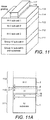
- FIG. 9 shows another example of a multi-junction solar cell, which makes use of the invention, this time illustrating all the cells.
- the Figure shows the tandem arrangement of the cells of the device (each of which is made up of various semiconductor layers, but these are not shown in detail).
- This device starts with a GaAs substrate 91 on which is grown a SiGe cell 92 in accordance with the invention (so comprising a SiGe layer having the p-n junction, a Si diffusion barrier layer and a III-V layer above (for example GaInP) that providing the doping, none of which are shown in detail in the Figure within the cell 92).
- a GaAs cell 94 and a InGaP cell 96 are provided.
- the cleave plane 12 may be formed using ion beam implant techniques to deposit hydrogen or helium atoms at a precise depth determined by the beam particle energy, for example at depths of up to about 1.5 ⁇ m, making the technique practical in the present context if the thickness of the layer of SiGe is of approximately this thickness.
Landscapes
- Photovoltaic Devices (AREA)
- Life Sciences & Earth Sciences (AREA)
- Engineering & Computer Science (AREA)
- Sustainable Energy (AREA)
- Sustainable Development (AREA)
- Recrystallisation Techniques (AREA)
- Chemical & Material Sciences (AREA)
- Crystallography & Structural Chemistry (AREA)
Applications Claiming Priority (2)
| Application Number | Priority Date | Filing Date | Title |
|---|---|---|---|
| US201161528650P | 2011-08-29 | 2011-08-29 | |
| PCT/GB2012/051982 WO2013030531A1 (en) | 2011-08-29 | 2012-08-14 | Photovoltaic device |
Publications (2)
| Publication Number | Publication Date |
|---|---|
| EP2745330A1 EP2745330A1 (en) | 2014-06-25 |
| EP2745330B1 true EP2745330B1 (en) | 2020-06-03 |
Family
ID=46727255
Family Applications (3)
| Application Number | Title | Priority Date | Filing Date |
|---|---|---|---|
| EP12753571.4A Active EP2745330B1 (en) | 2011-08-29 | 2012-08-14 | Photovoltaic device |
| EP12750801.8A Not-in-force EP2745329B1 (en) | 2011-08-29 | 2012-08-14 | Photovoltaic device |
| EP12750800.0A Ceased EP2745328A1 (en) | 2011-08-29 | 2012-08-14 | Photovoltaic device |
Family Applications After (2)
| Application Number | Title | Priority Date | Filing Date |
|---|---|---|---|
| EP12750801.8A Not-in-force EP2745329B1 (en) | 2011-08-29 | 2012-08-14 | Photovoltaic device |
| EP12750800.0A Ceased EP2745328A1 (en) | 2011-08-29 | 2012-08-14 | Photovoltaic device |
Country Status (7)
| Country | Link |
|---|---|
| US (4) | US20140345679A1 (OSRAM) |
| EP (3) | EP2745330B1 (OSRAM) |
| JP (3) | JP6228119B2 (OSRAM) |
| CN (2) | CN103875079B (OSRAM) |
| AU (2) | AU2012300694C1 (OSRAM) |
| ES (1) | ES2813938T3 (OSRAM) |
| WO (3) | WO2013030531A1 (OSRAM) |
Families Citing this family (35)
| Publication number | Priority date | Publication date | Assignee | Title |
|---|---|---|---|---|
| US20170141256A1 (en) * | 2009-10-23 | 2017-05-18 | Alta Devices, Inc. | Multi-junction optoelectronic device with group iv semiconductor as a bottom junction |
| US11646388B2 (en) | 2012-09-14 | 2023-05-09 | The Boeing Company | Group-IV solar cell structure using group-IV or III-V heterostructures |
| US9099595B2 (en) | 2012-09-14 | 2015-08-04 | The Boeing Company | Group-IV solar cell structure using group-IV or III-V heterostructures |
| US9985160B2 (en) * | 2012-09-14 | 2018-05-29 | The Boeing Company | Group-IV solar cell structure using group-IV or III-V heterostructures |
| US9997659B2 (en) | 2012-09-14 | 2018-06-12 | The Boeing Company | Group-IV solar cell structure using group-IV or III-V heterostructures |
| US11495705B2 (en) | 2012-09-14 | 2022-11-08 | The Boeing Company | Group-IV solar cell structure using group-IV or III-V heterostructures |
| US10903383B2 (en) | 2012-09-14 | 2021-01-26 | The Boeing Company | Group-IV solar cell structure using group-IV or III-V heterostructures |
| KR20140095738A (ko) * | 2013-01-25 | 2014-08-04 | 삼성전자주식회사 | 트랜지스터 및 그 제조 방법 |
| CN103199130B (zh) * | 2013-03-15 | 2016-03-09 | 中国科学院苏州纳米技术与纳米仿生研究所 | 正装四结太阳电池及其制备方法 |
| CN103199141A (zh) * | 2013-03-15 | 2013-07-10 | 中国科学院苏州纳米技术与纳米仿生研究所 | 四结级联太阳能电池及其制备方法 |
| CN103137766B (zh) * | 2013-03-15 | 2015-09-09 | 中国科学院苏州纳米技术与纳米仿生研究所 | 三结级联太阳电池及其制备方法 |
| EP2782145A1 (fr) * | 2013-03-21 | 2014-09-24 | Alcatel Lucent | Procédé de fabrication d'un dispositif photovoltaïque multi-jonctions et dispositif photovoltaïque multi-jonctions ainsi obtenu |
| CN103219412B (zh) * | 2013-04-03 | 2016-03-09 | 中国科学院苏州纳米技术与纳米仿生研究所 | 三结级联太阳电池及其制备方法 |
| CN103151414B (zh) * | 2013-04-03 | 2016-04-27 | 中国科学院苏州纳米技术与纳米仿生研究所 | 正装三结级联太阳电池及其制备方法 |
| CN103259193B (zh) * | 2013-05-14 | 2016-03-09 | 中国科学院苏州纳米技术与纳米仿生研究所 | 一种1300nm~1550nm含铋化物的半导体激光器的制备方法 |
| CN103311353B (zh) * | 2013-05-29 | 2016-09-07 | 中国科学院苏州纳米技术与纳米仿生研究所 | 三结级联太阳能电池及其制备方法 |
| GB2515322A (en) * | 2013-06-19 | 2014-12-24 | Univ Surrey | Light Receiving Device |
| US20140373906A1 (en) * | 2013-06-25 | 2014-12-25 | Solar Junction Corporation | Anti-reflection coatings for multijunction solar cells |
| CN103426965B (zh) * | 2013-08-16 | 2016-12-28 | 中国科学院苏州纳米技术与纳米仿生研究所 | 太阳能电池及其制作方法 |
| CN104638046B (zh) * | 2013-11-13 | 2017-05-03 | 中国电子科技集团公司第十八研究所 | Ge衬底异质结热光伏电池 |
| CN104638060B (zh) * | 2013-11-13 | 2018-03-06 | 中国电子科技集团公司第十八研究所 | 异质结热光伏电池的制备方法 |
| CN103839774A (zh) * | 2014-02-25 | 2014-06-04 | 清华大学 | SiGeSn层及其形成方法 |
| US9548408B2 (en) * | 2014-04-15 | 2017-01-17 | L-3 Communications Cincinnati Electronics Corporation | Tunneling barrier infrared detector devices |
| JP2016082041A (ja) * | 2014-10-15 | 2016-05-16 | 株式会社リコー | 化合物半導体太陽電池、及び、化合物半導体太陽電池の製造方法 |
| CN108604620A (zh) * | 2016-01-29 | 2018-09-28 | 奥塔装置公司 | 具有iv族半导体作为底部结的多结光电子器件 |
| CN105720126B (zh) * | 2016-04-27 | 2017-07-28 | 天津三安光电有限公司 | 一种倒装四结太阳能电池结构及其制备方法 |
| US20170365732A1 (en) | 2016-06-15 | 2017-12-21 | Solar Junction Corporation | Dilute nitride bismide semiconductor alloys |
| CN106531836A (zh) * | 2016-11-25 | 2017-03-22 | 罗雷 | 四结太阳能电池 |
| US10593818B2 (en) * | 2016-12-09 | 2020-03-17 | The Boeing Company | Multijunction solar cell having patterned emitter and method of making the solar cell |
| CN108807284B (zh) * | 2017-04-28 | 2020-06-26 | 环球晶圆股份有限公司 | 一种外延接合基板及其制造方法 |
| US11342498B2 (en) * | 2018-01-08 | 2022-05-24 | Integrated Silicon Solution (cayman) Inc. | High density 3D magnetic random access memory (MRAM) cell integration using wafer cut and transfer |
| CN111477677B (zh) * | 2020-05-27 | 2024-12-06 | 北京时代全芯存储技术股份有限公司 | 二极管结构及其制造方法 |
| CN113066907B (zh) * | 2021-06-03 | 2021-08-27 | 南昌凯迅光电有限公司 | 一种纳米网状表面电极的三结砷化镓太阳电池的制备方法 |
| EP4459682A1 (en) | 2023-05-03 | 2024-11-06 | Valstybinis moksliniu tyrimu institutas Fiziniu ir technologijos mokslu centras | Method for making multijunction photovoltaic device comprising a gaasbi subcell |
| CN118658918B (zh) * | 2024-07-19 | 2025-11-04 | 江苏仲磊芯半导体有限公司 | 一种四结太阳能电池及其制作方法 |
Family Cites Families (32)
| Publication number | Priority date | Publication date | Assignee | Title |
|---|---|---|---|---|
| WO1987002183A1 (en) * | 1985-09-30 | 1987-04-09 | Kanegafuchi Kagaku Kogyo Kabushiki Kaisha | Multijunction semiconductor device |
| JPS6437060A (en) * | 1987-08-03 | 1989-02-07 | Nippon Telegraph & Telephone | Semiconductor element |
| US6281426B1 (en) * | 1997-10-01 | 2001-08-28 | Midwest Research Institute | Multi-junction, monolithic solar cell using low-band-gap materials lattice matched to GaAs or Ge |
| US5944913A (en) * | 1997-11-26 | 1999-08-31 | Sandia Corporation | High-efficiency solar cell and method for fabrication |
| US6380601B1 (en) | 1999-03-29 | 2002-04-30 | Hughes Electronics Corporation | Multilayer semiconductor structure with phosphide-passivated germanium substrate |
| JP3657143B2 (ja) * | 1999-04-27 | 2005-06-08 | シャープ株式会社 | 太陽電池及びその製造方法 |
| US6252287B1 (en) * | 1999-05-19 | 2001-06-26 | Sandia Corporation | InGaAsN/GaAs heterojunction for multi-junction solar cells |
| US6340788B1 (en) * | 1999-12-02 | 2002-01-22 | Hughes Electronics Corporation | Multijunction photovoltaic cells and panels using a silicon or silicon-germanium active substrate cell for space and terrestrial applications |
| US7339109B2 (en) | 2000-06-20 | 2008-03-04 | Emcore Corporation | Apparatus and method for optimizing the efficiency of germanium junctions in multi-junction solar cells |
| JP2002222989A (ja) * | 2001-01-26 | 2002-08-09 | Toshiba Corp | 半導体発光素子 |
| US6815736B2 (en) * | 2001-02-09 | 2004-11-09 | Midwest Research Institute | Isoelectronic co-doping |
| US20030015728A1 (en) * | 2001-07-17 | 2003-01-23 | Motorola, Inc. | Photonic biasing and integrated solar charging networks for integrated circuits |
| US20060162768A1 (en) * | 2002-05-21 | 2006-07-27 | Wanlass Mark W | Low bandgap, monolithic, multi-bandgap, optoelectronic devices |
| US7126052B2 (en) * | 2002-10-02 | 2006-10-24 | The Boeing Company | Isoelectronic surfactant induced sublattice disordering in optoelectronic devices |
| CN100477289C (zh) * | 2004-01-20 | 2009-04-08 | 瑟雷姆技术公司 | 具有外延生长量子点材料的太阳能电池 |
| US10069026B2 (en) * | 2005-12-19 | 2018-09-04 | The Boeing Company | Reduced band gap absorber for solar cells |
| US7872252B2 (en) * | 2006-08-11 | 2011-01-18 | Cyrium Technologies Incorporated | Method of fabricating semiconductor devices on a group IV substrate with controlled interface properties and diffusion tails |
| US20080257405A1 (en) * | 2007-04-18 | 2008-10-23 | Emcore Corp. | Multijunction solar cell with strained-balanced quantum well middle cell |
| WO2009009111A2 (en) | 2007-07-10 | 2009-01-15 | The Board Of Trustees Of The Leland Stanford Junior University | GaInNAsSB SOLAR CELLS GROWN BY MOLECULAR BEAM EPITAXY |
| WO2009157870A1 (en) | 2008-06-26 | 2009-12-30 | Nanyang Technological University | Method for fabricating ganassb semiconductor |
| CN101431117A (zh) * | 2008-11-24 | 2009-05-13 | 北京索拉安吉清洁能源科技有限公司 | 具有掺杂阻挡层的多结太阳电池 |
| US20100147366A1 (en) * | 2008-12-17 | 2010-06-17 | Emcore Solar Power, Inc. | Inverted Metamorphic Multijunction Solar Cells with Distributed Bragg Reflector |
| GB2467935B (en) | 2009-02-19 | 2013-10-30 | Iqe Silicon Compounds Ltd | Formation of thin layers of GaAs and germanium materials |
| GB2467934B (en) | 2009-02-19 | 2013-10-30 | Iqe Silicon Compounds Ltd | Photovoltaic cell |
| WO2010102345A1 (en) * | 2009-03-12 | 2010-09-16 | Shaun Joseph Cunningham | Improved photo-voltaic device and system |
| US20100282306A1 (en) * | 2009-05-08 | 2010-11-11 | Emcore Solar Power, Inc. | Multijunction Solar Cells with Group IV/III-V Hybrid Alloys |
| US20100282307A1 (en) * | 2009-05-08 | 2010-11-11 | Emcore Solar Power, Inc. | Multijunction Solar Cells with Group IV/III-V Hybrid Alloys for Terrestrial Applications |
| US20100282305A1 (en) * | 2009-05-08 | 2010-11-11 | Emcore Solar Power, Inc. | Inverted Multijunction Solar Cells with Group IV/III-V Hybrid Alloys |
| TW201114043A (en) | 2009-10-02 | 2011-04-16 | Epistar Corp | A high efficiency solar cell |
| US20110232730A1 (en) | 2010-03-29 | 2011-09-29 | Solar Junction Corp. | Lattice matchable alloy for solar cells |
| US9214580B2 (en) | 2010-10-28 | 2015-12-15 | Solar Junction Corporation | Multi-junction solar cell with dilute nitride sub-cell having graded doping |
| WO2013074530A2 (en) * | 2011-11-15 | 2013-05-23 | Solar Junction Corporation | High efficiency multijunction solar cells |
-
2012
- 2012-08-14 US US14/342,016 patent/US20140345679A1/en not_active Abandoned
- 2012-08-14 CN CN201280049676.9A patent/CN103875079B/zh not_active Expired - Fee Related
- 2012-08-14 CN CN201711071248.7A patent/CN107845690B/zh not_active Expired - Fee Related
- 2012-08-14 EP EP12753571.4A patent/EP2745330B1/en active Active
- 2012-08-14 WO PCT/GB2012/051982 patent/WO2013030531A1/en not_active Ceased
- 2012-08-14 WO PCT/GB2012/051981 patent/WO2013030530A1/en not_active Ceased
- 2012-08-14 WO PCT/GB2012/051980 patent/WO2013030529A1/en not_active Ceased
- 2012-08-14 JP JP2014527730A patent/JP6228119B2/ja not_active Expired - Fee Related
- 2012-08-14 US US14/241,987 patent/US20150041863A1/en not_active Abandoned
- 2012-08-14 AU AU2012300694A patent/AU2012300694C1/en not_active Ceased
- 2012-08-14 EP EP12750801.8A patent/EP2745329B1/en not_active Not-in-force
- 2012-08-14 EP EP12750800.0A patent/EP2745328A1/en not_active Ceased
- 2012-08-14 US US14/342,061 patent/US10263129B2/en active Active
- 2012-08-14 ES ES12753571T patent/ES2813938T3/es active Active
-
2016
- 2016-01-19 AU AU2016200282A patent/AU2016200282B2/en not_active Ceased
- 2016-12-16 US US15/382,181 patent/US10367107B2/en active Active
-
2017
- 2017-10-12 JP JP2017198245A patent/JP2018026580A/ja active Pending
-
2019
- 2019-07-26 JP JP2019137470A patent/JP2019216249A/ja active Pending
Non-Patent Citations (1)
| Title |
|---|
| None * |
Also Published As
| Publication number | Publication date |
|---|---|
| WO2013030530A1 (en) | 2013-03-07 |
| US20150041863A1 (en) | 2015-02-12 |
| EP2745330A1 (en) | 2014-06-25 |
| EP2745329A1 (en) | 2014-06-25 |
| CN107845690B (zh) | 2020-09-08 |
| AU2016200282B2 (en) | 2017-08-31 |
| US20140326301A1 (en) | 2014-11-06 |
| AU2012300694A8 (en) | 2014-04-03 |
| AU2016200282A1 (en) | 2016-02-11 |
| CN103875079A (zh) | 2014-06-18 |
| JP2014527725A (ja) | 2014-10-16 |
| EP2745329B1 (en) | 2018-09-19 |
| JP2019216249A (ja) | 2019-12-19 |
| AU2012300694C1 (en) | 2016-04-21 |
| ES2813938T3 (es) | 2021-03-25 |
| AU2012300694B2 (en) | 2015-10-22 |
| WO2013030529A1 (en) | 2013-03-07 |
| AU2012300694A1 (en) | 2014-03-20 |
| WO2013030531A1 (en) | 2013-03-07 |
| US10367107B2 (en) | 2019-07-30 |
| EP2745328A1 (en) | 2014-06-25 |
| US10263129B2 (en) | 2019-04-16 |
| US20170117429A1 (en) | 2017-04-27 |
| CN107845690A (zh) | 2018-03-27 |
| JP6228119B2 (ja) | 2017-11-08 |
| US20140345679A1 (en) | 2014-11-27 |
| CN103875079B (zh) | 2017-12-12 |
| JP2018026580A (ja) | 2018-02-15 |
Similar Documents
| Publication | Publication Date | Title |
|---|---|---|
| EP2745330B1 (en) | Photovoltaic device | |
| EP2399300B1 (en) | Method for forming a photovoltaic cell | |
| US8344242B2 (en) | Multi-junction solar cells | |
| US10680126B2 (en) | Photovoltaics on silicon | |
| US9716201B2 (en) | Silicon heterojunction photovoltaic device with wide band gap emitter | |
| US20090288703A1 (en) | Wide Band Gap Window Layers In Inverted Metamorphic Multijunction Solar Cells | |
| US20140196774A1 (en) | Multi-junction iii-v solar cell | |
| KR20210021435A (ko) | 격자-정합 희석 질화물 접합을 포함하는 가요성 박막 멀티-접합 광전자 장치 및 그 제조 방법 | |
| GB2501432A (en) | Germanium Based Photovoltaic Cell With GaAs Substrate Removed |
Legal Events
| Date | Code | Title | Description |
|---|---|---|---|
| PUAI | Public reference made under article 153(3) epc to a published international application that has entered the european phase |
Free format text: ORIGINAL CODE: 0009012 |
|
| 17P | Request for examination filed |
Effective date: 20140321 |
|
| AK | Designated contracting states |
Kind code of ref document: A1 Designated state(s): AL AT BE BG CH CY CZ DE DK EE ES FI FR GB GR HR HU IE IS IT LI LT LU LV MC MK MT NL NO PL PT RO RS SE SI SK SM TR |
|
| DAX | Request for extension of the european patent (deleted) | ||
| STAA | Information on the status of an ep patent application or granted ep patent |
Free format text: STATUS: EXAMINATION IS IN PROGRESS |
|
| 17Q | First examination report despatched |
Effective date: 20170919 |
|
| GRAP | Despatch of communication of intention to grant a patent |
Free format text: ORIGINAL CODE: EPIDOSNIGR1 |
|
| STAA | Information on the status of an ep patent application or granted ep patent |
Free format text: STATUS: GRANT OF PATENT IS INTENDED |
|
| INTG | Intention to grant announced |
Effective date: 20191213 |
|
| GRAS | Grant fee paid |
Free format text: ORIGINAL CODE: EPIDOSNIGR3 |
|
| GRAA | (expected) grant |
Free format text: ORIGINAL CODE: 0009210 |
|
| STAA | Information on the status of an ep patent application or granted ep patent |
Free format text: STATUS: THE PATENT HAS BEEN GRANTED |
|
| AK | Designated contracting states |
Kind code of ref document: B1 Designated state(s): AL AT BE BG CH CY CZ DE DK EE ES FI FR GB GR HR HU IE IS IT LI LT LU LV MC MK MT NL NO PL PT RO RS SE SI SK SM TR |
|
| REG | Reference to a national code |
Ref country code: GB Ref legal event code: FG4D |
|
| REG | Reference to a national code |
Ref country code: AT Ref legal event code: REF Ref document number: 1277931 Country of ref document: AT Kind code of ref document: T Effective date: 20200615 Ref country code: CH Ref legal event code: EP |
|
| REG | Reference to a national code |
Ref country code: DE Ref legal event code: R096 Ref document number: 602012070475 Country of ref document: DE |
|
| REG | Reference to a national code |
Ref country code: NL Ref legal event code: FP |
|
| REG | Reference to a national code |
Ref country code: FI Ref legal event code: FGE |
|
| REG | Reference to a national code |
Ref country code: LT Ref legal event code: MG4D |
|
| PG25 | Lapsed in a contracting state [announced via postgrant information from national office to epo] |
Ref country code: GR Free format text: LAPSE BECAUSE OF FAILURE TO SUBMIT A TRANSLATION OF THE DESCRIPTION OR TO PAY THE FEE WITHIN THE PRESCRIBED TIME-LIMIT Effective date: 20200904 Ref country code: NO Free format text: LAPSE BECAUSE OF FAILURE TO SUBMIT A TRANSLATION OF THE DESCRIPTION OR TO PAY THE FEE WITHIN THE PRESCRIBED TIME-LIMIT Effective date: 20200903 Ref country code: SE Free format text: LAPSE BECAUSE OF FAILURE TO SUBMIT A TRANSLATION OF THE DESCRIPTION OR TO PAY THE FEE WITHIN THE PRESCRIBED TIME-LIMIT Effective date: 20200603 Ref country code: LT Free format text: LAPSE BECAUSE OF FAILURE TO SUBMIT A TRANSLATION OF THE DESCRIPTION OR TO PAY THE FEE WITHIN THE PRESCRIBED TIME-LIMIT Effective date: 20200603 |
|
| PG25 | Lapsed in a contracting state [announced via postgrant information from national office to epo] |
Ref country code: RS Free format text: LAPSE BECAUSE OF FAILURE TO SUBMIT A TRANSLATION OF THE DESCRIPTION OR TO PAY THE FEE WITHIN THE PRESCRIBED TIME-LIMIT Effective date: 20200603 Ref country code: BG Free format text: LAPSE BECAUSE OF FAILURE TO SUBMIT A TRANSLATION OF THE DESCRIPTION OR TO PAY THE FEE WITHIN THE PRESCRIBED TIME-LIMIT Effective date: 20200903 Ref country code: LV Free format text: LAPSE BECAUSE OF FAILURE TO SUBMIT A TRANSLATION OF THE DESCRIPTION OR TO PAY THE FEE WITHIN THE PRESCRIBED TIME-LIMIT Effective date: 20200603 Ref country code: HR Free format text: LAPSE BECAUSE OF FAILURE TO SUBMIT A TRANSLATION OF THE DESCRIPTION OR TO PAY THE FEE WITHIN THE PRESCRIBED TIME-LIMIT Effective date: 20200603 |
|
| REG | Reference to a national code |
Ref country code: AT Ref legal event code: MK05 Ref document number: 1277931 Country of ref document: AT Kind code of ref document: T Effective date: 20200603 |
|
| PG25 | Lapsed in a contracting state [announced via postgrant information from national office to epo] |
Ref country code: AL Free format text: LAPSE BECAUSE OF FAILURE TO SUBMIT A TRANSLATION OF THE DESCRIPTION OR TO PAY THE FEE WITHIN THE PRESCRIBED TIME-LIMIT Effective date: 20200603 |
|
| PG25 | Lapsed in a contracting state [announced via postgrant information from national office to epo] |
Ref country code: EE Free format text: LAPSE BECAUSE OF FAILURE TO SUBMIT A TRANSLATION OF THE DESCRIPTION OR TO PAY THE FEE WITHIN THE PRESCRIBED TIME-LIMIT Effective date: 20200603 Ref country code: SM Free format text: LAPSE BECAUSE OF FAILURE TO SUBMIT A TRANSLATION OF THE DESCRIPTION OR TO PAY THE FEE WITHIN THE PRESCRIBED TIME-LIMIT Effective date: 20200603 Ref country code: AT Free format text: LAPSE BECAUSE OF FAILURE TO SUBMIT A TRANSLATION OF THE DESCRIPTION OR TO PAY THE FEE WITHIN THE PRESCRIBED TIME-LIMIT Effective date: 20200603 Ref country code: PT Free format text: LAPSE BECAUSE OF FAILURE TO SUBMIT A TRANSLATION OF THE DESCRIPTION OR TO PAY THE FEE WITHIN THE PRESCRIBED TIME-LIMIT Effective date: 20201006 Ref country code: RO Free format text: LAPSE BECAUSE OF FAILURE TO SUBMIT A TRANSLATION OF THE DESCRIPTION OR TO PAY THE FEE WITHIN THE PRESCRIBED TIME-LIMIT Effective date: 20200603 Ref country code: CZ Free format text: LAPSE BECAUSE OF FAILURE TO SUBMIT A TRANSLATION OF THE DESCRIPTION OR TO PAY THE FEE WITHIN THE PRESCRIBED TIME-LIMIT Effective date: 20200603 |
|
| PG25 | Lapsed in a contracting state [announced via postgrant information from national office to epo] |
Ref country code: IS Free format text: LAPSE BECAUSE OF FAILURE TO SUBMIT A TRANSLATION OF THE DESCRIPTION OR TO PAY THE FEE WITHIN THE PRESCRIBED TIME-LIMIT Effective date: 20201003 Ref country code: PL Free format text: LAPSE BECAUSE OF FAILURE TO SUBMIT A TRANSLATION OF THE DESCRIPTION OR TO PAY THE FEE WITHIN THE PRESCRIBED TIME-LIMIT Effective date: 20200603 Ref country code: SK Free format text: LAPSE BECAUSE OF FAILURE TO SUBMIT A TRANSLATION OF THE DESCRIPTION OR TO PAY THE FEE WITHIN THE PRESCRIBED TIME-LIMIT Effective date: 20200603 |
|
| REG | Reference to a national code |
Ref country code: DE Ref legal event code: R097 Ref document number: 602012070475 Country of ref document: DE |
|
| REG | Reference to a national code |
Ref country code: ES Ref legal event code: FG2A Ref document number: 2813938 Country of ref document: ES Kind code of ref document: T3 Effective date: 20210325 |
|
| PG25 | Lapsed in a contracting state [announced via postgrant information from national office to epo] |
Ref country code: MC Free format text: LAPSE BECAUSE OF FAILURE TO SUBMIT A TRANSLATION OF THE DESCRIPTION OR TO PAY THE FEE WITHIN THE PRESCRIBED TIME-LIMIT Effective date: 20200603 |
|
| REG | Reference to a national code |
Ref country code: CH Ref legal event code: PL |
|
| PLBE | No opposition filed within time limit |
Free format text: ORIGINAL CODE: 0009261 |
|
| STAA | Information on the status of an ep patent application or granted ep patent |
Free format text: STATUS: NO OPPOSITION FILED WITHIN TIME LIMIT |
|
| PG25 | Lapsed in a contracting state [announced via postgrant information from national office to epo] |
Ref country code: CH Free format text: LAPSE BECAUSE OF NON-PAYMENT OF DUE FEES Effective date: 20200831 Ref country code: DK Free format text: LAPSE BECAUSE OF FAILURE TO SUBMIT A TRANSLATION OF THE DESCRIPTION OR TO PAY THE FEE WITHIN THE PRESCRIBED TIME-LIMIT Effective date: 20200603 Ref country code: LI Free format text: LAPSE BECAUSE OF NON-PAYMENT OF DUE FEES Effective date: 20200831 Ref country code: LU Free format text: LAPSE BECAUSE OF NON-PAYMENT OF DUE FEES Effective date: 20200814 |
|
| 26N | No opposition filed |
Effective date: 20210304 |
|
| PG25 | Lapsed in a contracting state [announced via postgrant information from national office to epo] |
Ref country code: SI Free format text: LAPSE BECAUSE OF FAILURE TO SUBMIT A TRANSLATION OF THE DESCRIPTION OR TO PAY THE FEE WITHIN THE PRESCRIBED TIME-LIMIT Effective date: 20200603 |
|
| PG25 | Lapsed in a contracting state [announced via postgrant information from national office to epo] |
Ref country code: IE Free format text: LAPSE BECAUSE OF NON-PAYMENT OF DUE FEES Effective date: 20200814 |
|
| PGFP | Annual fee paid to national office [announced via postgrant information from national office to epo] |
Ref country code: NL Payment date: 20210813 Year of fee payment: 10 |
|
| PG25 | Lapsed in a contracting state [announced via postgrant information from national office to epo] |
Ref country code: TR Free format text: LAPSE BECAUSE OF FAILURE TO SUBMIT A TRANSLATION OF THE DESCRIPTION OR TO PAY THE FEE WITHIN THE PRESCRIBED TIME-LIMIT Effective date: 20200603 Ref country code: MT Free format text: LAPSE BECAUSE OF FAILURE TO SUBMIT A TRANSLATION OF THE DESCRIPTION OR TO PAY THE FEE WITHIN THE PRESCRIBED TIME-LIMIT Effective date: 20200603 Ref country code: CY Free format text: LAPSE BECAUSE OF FAILURE TO SUBMIT A TRANSLATION OF THE DESCRIPTION OR TO PAY THE FEE WITHIN THE PRESCRIBED TIME-LIMIT Effective date: 20200603 |
|
| PG25 | Lapsed in a contracting state [announced via postgrant information from national office to epo] |
Ref country code: MK Free format text: LAPSE BECAUSE OF FAILURE TO SUBMIT A TRANSLATION OF THE DESCRIPTION OR TO PAY THE FEE WITHIN THE PRESCRIBED TIME-LIMIT Effective date: 20200603 |
|
| PGFP | Annual fee paid to national office [announced via postgrant information from national office to epo] |
Ref country code: FI Payment date: 20220928 Year of fee payment: 11 |
|
| REG | Reference to a national code |
Ref country code: NL Ref legal event code: MM Effective date: 20220901 |
|
| P01 | Opt-out of the competence of the unified patent court (upc) registered |
Effective date: 20230321 |
|
| PG25 | Lapsed in a contracting state [announced via postgrant information from national office to epo] |
Ref country code: NL Free format text: LAPSE BECAUSE OF NON-PAYMENT OF DUE FEES Effective date: 20220901 |
|
| PGFP | Annual fee paid to national office [announced via postgrant information from national office to epo] |
Ref country code: IT Payment date: 20230822 Year of fee payment: 12 Ref country code: GB Payment date: 20230828 Year of fee payment: 12 Ref country code: ES Payment date: 20230901 Year of fee payment: 12 |
|
| PGFP | Annual fee paid to national office [announced via postgrant information from national office to epo] |
Ref country code: FR Payment date: 20230825 Year of fee payment: 12 Ref country code: DE Payment date: 20230829 Year of fee payment: 12 Ref country code: BE Payment date: 20230828 Year of fee payment: 12 |
|
| PG25 | Lapsed in a contracting state [announced via postgrant information from national office to epo] |
Ref country code: FI Free format text: LAPSE BECAUSE OF NON-PAYMENT OF DUE FEES Effective date: 20230814 |
|
| REG | Reference to a national code |
Ref country code: DE Ref legal event code: R079 Ref document number: 602012070475 Country of ref document: DE Free format text: PREVIOUS MAIN CLASS: H01L0031032800 Ipc: H10F0077120000 |
|
| REG | Reference to a national code |
Ref country code: DE Ref legal event code: R119 Ref document number: 602012070475 Country of ref document: DE |
|
| GBPC | Gb: european patent ceased through non-payment of renewal fee |
Effective date: 20240814 |
|
| REG | Reference to a national code |
Ref country code: BE Ref legal event code: MM Effective date: 20240831 |
|
| PG25 | Lapsed in a contracting state [announced via postgrant information from national office to epo] |
Ref country code: DE Free format text: LAPSE BECAUSE OF NON-PAYMENT OF DUE FEES Effective date: 20250301 |
|
| PG25 | Lapsed in a contracting state [announced via postgrant information from national office to epo] |
Ref country code: GB Free format text: LAPSE BECAUSE OF NON-PAYMENT OF DUE FEES Effective date: 20240814 |
|
| PG25 | Lapsed in a contracting state [announced via postgrant information from national office to epo] |
Ref country code: IT Free format text: LAPSE BECAUSE OF NON-PAYMENT OF DUE FEES Effective date: 20240814 Ref country code: BE Free format text: LAPSE BECAUSE OF NON-PAYMENT OF DUE FEES Effective date: 20240831 |
|
| PG25 | Lapsed in a contracting state [announced via postgrant information from national office to epo] |
Ref country code: FR Free format text: LAPSE BECAUSE OF NON-PAYMENT OF DUE FEES Effective date: 20240831 |
|
| REG | Reference to a national code |
Ref country code: ES Ref legal event code: FD2A Effective date: 20250926 |
|
| PG25 | Lapsed in a contracting state [announced via postgrant information from national office to epo] |
Ref country code: ES Free format text: LAPSE BECAUSE OF NON-PAYMENT OF DUE FEES Effective date: 20240815 |