EP2728037B1 - Gehäuserahmen und Herstellungsverfahren dafür - Google Patents
Gehäuserahmen und Herstellungsverfahren dafür Download PDFInfo
- Publication number
- EP2728037B1 EP2728037B1 EP13191267.7A EP13191267A EP2728037B1 EP 2728037 B1 EP2728037 B1 EP 2728037B1 EP 13191267 A EP13191267 A EP 13191267A EP 2728037 B1 EP2728037 B1 EP 2728037B1
- Authority
- EP
- European Patent Office
- Prior art keywords
- layer
- deposition
- case frame
- sio
- transparent
- Prior art date
- Legal status (The legal status is an assumption and is not a legal conclusion. Google has not performed a legal analysis and makes no representation as to the accuracy of the status listed.)
- Not-in-force
Links
Images


Classifications
-
- H—ELECTRICITY
- H05—ELECTRIC TECHNIQUES NOT OTHERWISE PROVIDED FOR
- H05K—PRINTED CIRCUITS; CASINGS OR CONSTRUCTIONAL DETAILS OF ELECTRIC APPARATUS; MANUFACTURE OF ASSEMBLAGES OF ELECTRICAL COMPONENTS
- H05K5/00—Casings, cabinets or drawers for electric apparatus
- H05K5/02—Details
-
- H—ELECTRICITY
- H05—ELECTRIC TECHNIQUES NOT OTHERWISE PROVIDED FOR
- H05K—PRINTED CIRCUITS; CASINGS OR CONSTRUCTIONAL DETAILS OF ELECTRIC APPARATUS; MANUFACTURE OF ASSEMBLAGES OF ELECTRICAL COMPONENTS
- H05K5/00—Casings, cabinets or drawers for electric apparatus
- H05K5/02—Details
- H05K5/0217—Mechanical details of casings
- H05K5/0243—Mechanical details of casings for decorative purposes
-
- B—PERFORMING OPERATIONS; TRANSPORTING
- B32—LAYERED PRODUCTS
- B32B—LAYERED PRODUCTS, i.e. PRODUCTS BUILT-UP OF STRATA OF FLAT OR NON-FLAT, e.g. CELLULAR OR HONEYCOMB, FORM
- B32B9/00—Layered products comprising a layer of a particular substance not covered by groups B32B11/00 - B32B29/00
- B32B9/04—Layered products comprising a layer of a particular substance not covered by groups B32B11/00 - B32B29/00 comprising such particular substance as the main or only constituent of a layer, which is next to another layer of the same or of a different material
-
- B—PERFORMING OPERATIONS; TRANSPORTING
- B44—DECORATIVE ARTS
- B44C—PRODUCING DECORATIVE EFFECTS; MOSAICS; TARSIA WORK; PAPERHANGING
- B44C3/00—Processes, not specifically provided for elsewhere, for producing ornamental structures
- B44C3/02—Superimposing layers
-
- C—CHEMISTRY; METALLURGY
- C23—COATING METALLIC MATERIAL; COATING MATERIAL WITH METALLIC MATERIAL; CHEMICAL SURFACE TREATMENT; DIFFUSION TREATMENT OF METALLIC MATERIAL; COATING BY VACUUM EVAPORATION, BY SPUTTERING, BY ION IMPLANTATION OR BY CHEMICAL VAPOUR DEPOSITION, IN GENERAL; INHIBITING CORROSION OF METALLIC MATERIAL OR INCRUSTATION IN GENERAL
- C23C—COATING METALLIC MATERIAL; COATING MATERIAL WITH METALLIC MATERIAL; SURFACE TREATMENT OF METALLIC MATERIAL BY DIFFUSION INTO THE SURFACE, BY CHEMICAL CONVERSION OR SUBSTITUTION; COATING BY VACUUM EVAPORATION, BY SPUTTERING, BY ION IMPLANTATION OR BY CHEMICAL VAPOUR DEPOSITION, IN GENERAL
- C23C14/00—Coating by vacuum evaporation, by sputtering or by ion implantation of the coating forming material
- C23C14/0015—Coating by vacuum evaporation, by sputtering or by ion implantation of the coating forming material characterized by the colour of the layer
-
- C—CHEMISTRY; METALLURGY
- C23—COATING METALLIC MATERIAL; COATING MATERIAL WITH METALLIC MATERIAL; CHEMICAL SURFACE TREATMENT; DIFFUSION TREATMENT OF METALLIC MATERIAL; COATING BY VACUUM EVAPORATION, BY SPUTTERING, BY ION IMPLANTATION OR BY CHEMICAL VAPOUR DEPOSITION, IN GENERAL; INHIBITING CORROSION OF METALLIC MATERIAL OR INCRUSTATION IN GENERAL
- C23C—COATING METALLIC MATERIAL; COATING MATERIAL WITH METALLIC MATERIAL; SURFACE TREATMENT OF METALLIC MATERIAL BY DIFFUSION INTO THE SURFACE, BY CHEMICAL CONVERSION OR SUBSTITUTION; COATING BY VACUUM EVAPORATION, BY SPUTTERING, BY ION IMPLANTATION OR BY CHEMICAL VAPOUR DEPOSITION, IN GENERAL
- C23C14/00—Coating by vacuum evaporation, by sputtering or by ion implantation of the coating forming material
- C23C14/06—Coating by vacuum evaporation, by sputtering or by ion implantation of the coating forming material characterised by the coating material
- C23C14/08—Oxides
- C23C14/081—Oxides of aluminium, magnesium or beryllium
-
- C—CHEMISTRY; METALLURGY
- C23—COATING METALLIC MATERIAL; COATING MATERIAL WITH METALLIC MATERIAL; CHEMICAL SURFACE TREATMENT; DIFFUSION TREATMENT OF METALLIC MATERIAL; COATING BY VACUUM EVAPORATION, BY SPUTTERING, BY ION IMPLANTATION OR BY CHEMICAL VAPOUR DEPOSITION, IN GENERAL; INHIBITING CORROSION OF METALLIC MATERIAL OR INCRUSTATION IN GENERAL
- C23C—COATING METALLIC MATERIAL; COATING MATERIAL WITH METALLIC MATERIAL; SURFACE TREATMENT OF METALLIC MATERIAL BY DIFFUSION INTO THE SURFACE, BY CHEMICAL CONVERSION OR SUBSTITUTION; COATING BY VACUUM EVAPORATION, BY SPUTTERING, BY ION IMPLANTATION OR BY CHEMICAL VAPOUR DEPOSITION, IN GENERAL
- C23C14/00—Coating by vacuum evaporation, by sputtering or by ion implantation of the coating forming material
- C23C14/06—Coating by vacuum evaporation, by sputtering or by ion implantation of the coating forming material characterised by the coating material
- C23C14/08—Oxides
- C23C14/083—Oxides of refractory metals or yttrium
-
- C—CHEMISTRY; METALLURGY
- C23—COATING METALLIC MATERIAL; COATING MATERIAL WITH METALLIC MATERIAL; CHEMICAL SURFACE TREATMENT; DIFFUSION TREATMENT OF METALLIC MATERIAL; COATING BY VACUUM EVAPORATION, BY SPUTTERING, BY ION IMPLANTATION OR BY CHEMICAL VAPOUR DEPOSITION, IN GENERAL; INHIBITING CORROSION OF METALLIC MATERIAL OR INCRUSTATION IN GENERAL
- C23C—COATING METALLIC MATERIAL; COATING MATERIAL WITH METALLIC MATERIAL; SURFACE TREATMENT OF METALLIC MATERIAL BY DIFFUSION INTO THE SURFACE, BY CHEMICAL CONVERSION OR SUBSTITUTION; COATING BY VACUUM EVAPORATION, BY SPUTTERING, BY ION IMPLANTATION OR BY CHEMICAL VAPOUR DEPOSITION, IN GENERAL
- C23C14/00—Coating by vacuum evaporation, by sputtering or by ion implantation of the coating forming material
- C23C14/06—Coating by vacuum evaporation, by sputtering or by ion implantation of the coating forming material characterised by the coating material
- C23C14/10—Glass or silica
-
- C—CHEMISTRY; METALLURGY
- C23—COATING METALLIC MATERIAL; COATING MATERIAL WITH METALLIC MATERIAL; CHEMICAL SURFACE TREATMENT; DIFFUSION TREATMENT OF METALLIC MATERIAL; COATING BY VACUUM EVAPORATION, BY SPUTTERING, BY ION IMPLANTATION OR BY CHEMICAL VAPOUR DEPOSITION, IN GENERAL; INHIBITING CORROSION OF METALLIC MATERIAL OR INCRUSTATION IN GENERAL
- C23C—COATING METALLIC MATERIAL; COATING MATERIAL WITH METALLIC MATERIAL; SURFACE TREATMENT OF METALLIC MATERIAL BY DIFFUSION INTO THE SURFACE, BY CHEMICAL CONVERSION OR SUBSTITUTION; COATING BY VACUUM EVAPORATION, BY SPUTTERING, BY ION IMPLANTATION OR BY CHEMICAL VAPOUR DEPOSITION, IN GENERAL
- C23C14/00—Coating by vacuum evaporation, by sputtering or by ion implantation of the coating forming material
- C23C14/22—Coating by vacuum evaporation, by sputtering or by ion implantation of the coating forming material characterised by the process of coating
- C23C14/24—Vacuum evaporation
- C23C14/28—Vacuum evaporation by wave energy or particle radiation
- C23C14/30—Vacuum evaporation by wave energy or particle radiation by electron bombardment
-
- C—CHEMISTRY; METALLURGY
- C23—COATING METALLIC MATERIAL; COATING MATERIAL WITH METALLIC MATERIAL; CHEMICAL SURFACE TREATMENT; DIFFUSION TREATMENT OF METALLIC MATERIAL; COATING BY VACUUM EVAPORATION, BY SPUTTERING, BY ION IMPLANTATION OR BY CHEMICAL VAPOUR DEPOSITION, IN GENERAL; INHIBITING CORROSION OF METALLIC MATERIAL OR INCRUSTATION IN GENERAL
- C23C—COATING METALLIC MATERIAL; COATING MATERIAL WITH METALLIC MATERIAL; SURFACE TREATMENT OF METALLIC MATERIAL BY DIFFUSION INTO THE SURFACE, BY CHEMICAL CONVERSION OR SUBSTITUTION; COATING BY VACUUM EVAPORATION, BY SPUTTERING, BY ION IMPLANTATION OR BY CHEMICAL VAPOUR DEPOSITION, IN GENERAL
- C23C28/00—Coating for obtaining at least two superposed coatings either by methods not provided for in a single one of groups C23C2/00 - C23C26/00 or by combinations of methods provided for in subclasses C23C and C25C or C25D
-
- C—CHEMISTRY; METALLURGY
- C23—COATING METALLIC MATERIAL; COATING MATERIAL WITH METALLIC MATERIAL; CHEMICAL SURFACE TREATMENT; DIFFUSION TREATMENT OF METALLIC MATERIAL; COATING BY VACUUM EVAPORATION, BY SPUTTERING, BY ION IMPLANTATION OR BY CHEMICAL VAPOUR DEPOSITION, IN GENERAL; INHIBITING CORROSION OF METALLIC MATERIAL OR INCRUSTATION IN GENERAL
- C23C—COATING METALLIC MATERIAL; COATING MATERIAL WITH METALLIC MATERIAL; SURFACE TREATMENT OF METALLIC MATERIAL BY DIFFUSION INTO THE SURFACE, BY CHEMICAL CONVERSION OR SUBSTITUTION; COATING BY VACUUM EVAPORATION, BY SPUTTERING, BY ION IMPLANTATION OR BY CHEMICAL VAPOUR DEPOSITION, IN GENERAL
- C23C28/00—Coating for obtaining at least two superposed coatings either by methods not provided for in a single one of groups C23C2/00 - C23C26/00 or by combinations of methods provided for in subclasses C23C and C25C or C25D
- C23C28/40—Coatings including alternating layers following a pattern, a periodic or defined repetition
- C23C28/42—Coatings including alternating layers following a pattern, a periodic or defined repetition characterized by the composition of the alternating layers
-
- C—CHEMISTRY; METALLURGY
- C23—COATING METALLIC MATERIAL; COATING MATERIAL WITH METALLIC MATERIAL; CHEMICAL SURFACE TREATMENT; DIFFUSION TREATMENT OF METALLIC MATERIAL; COATING BY VACUUM EVAPORATION, BY SPUTTERING, BY ION IMPLANTATION OR BY CHEMICAL VAPOUR DEPOSITION, IN GENERAL; INHIBITING CORROSION OF METALLIC MATERIAL OR INCRUSTATION IN GENERAL
- C23C—COATING METALLIC MATERIAL; COATING MATERIAL WITH METALLIC MATERIAL; SURFACE TREATMENT OF METALLIC MATERIAL BY DIFFUSION INTO THE SURFACE, BY CHEMICAL CONVERSION OR SUBSTITUTION; COATING BY VACUUM EVAPORATION, BY SPUTTERING, BY ION IMPLANTATION OR BY CHEMICAL VAPOUR DEPOSITION, IN GENERAL
- C23C28/00—Coating for obtaining at least two superposed coatings either by methods not provided for in a single one of groups C23C2/00 - C23C26/00 or by combinations of methods provided for in subclasses C23C and C25C or C25D
- C23C28/40—Coatings including alternating layers following a pattern, a periodic or defined repetition
- C23C28/44—Coatings including alternating layers following a pattern, a periodic or defined repetition characterized by a measurable physical property of the alternating layer or system, e.g. thickness, density, hardness
-
- B—PERFORMING OPERATIONS; TRANSPORTING
- B32—LAYERED PRODUCTS
- B32B—LAYERED PRODUCTS, i.e. PRODUCTS BUILT-UP OF STRATA OF FLAT OR NON-FLAT, e.g. CELLULAR OR HONEYCOMB, FORM
- B32B15/00—Layered products comprising a layer of metal
- B32B15/04—Layered products comprising a layer of metal comprising metal as the main or only constituent of a layer, which is next to another layer of the same or of a different material
-
- B—PERFORMING OPERATIONS; TRANSPORTING
- B32—LAYERED PRODUCTS
- B32B—LAYERED PRODUCTS, i.e. PRODUCTS BUILT-UP OF STRATA OF FLAT OR NON-FLAT, e.g. CELLULAR OR HONEYCOMB, FORM
- B32B17/00—Layered products essentially comprising sheet glass, or glass, slag, or like fibres
- B32B17/06—Layered products essentially comprising sheet glass, or glass, slag, or like fibres comprising glass as the main or only constituent of a layer, next to another layer of a specific material
-
- B—PERFORMING OPERATIONS; TRANSPORTING
- B32—LAYERED PRODUCTS
- B32B—LAYERED PRODUCTS, i.e. PRODUCTS BUILT-UP OF STRATA OF FLAT OR NON-FLAT, e.g. CELLULAR OR HONEYCOMB, FORM
- B32B18/00—Layered products essentially comprising ceramics, e.g. refractory products
-
- B—PERFORMING OPERATIONS; TRANSPORTING
- B32—LAYERED PRODUCTS
- B32B—LAYERED PRODUCTS, i.e. PRODUCTS BUILT-UP OF STRATA OF FLAT OR NON-FLAT, e.g. CELLULAR OR HONEYCOMB, FORM
- B32B27/00—Layered products comprising a layer of synthetic resin
- B32B27/06—Layered products comprising a layer of synthetic resin as the main or only constituent of a layer, which is next to another layer of the same or of a different material
-
- B—PERFORMING OPERATIONS; TRANSPORTING
- B32—LAYERED PRODUCTS
- B32B—LAYERED PRODUCTS, i.e. PRODUCTS BUILT-UP OF STRATA OF FLAT OR NON-FLAT, e.g. CELLULAR OR HONEYCOMB, FORM
- B32B27/00—Layered products comprising a layer of synthetic resin
- B32B27/40—Layered products comprising a layer of synthetic resin comprising polyurethanes
-
- B—PERFORMING OPERATIONS; TRANSPORTING
- B32—LAYERED PRODUCTS
- B32B—LAYERED PRODUCTS, i.e. PRODUCTS BUILT-UP OF STRATA OF FLAT OR NON-FLAT, e.g. CELLULAR OR HONEYCOMB, FORM
- B32B3/00—Layered products comprising a layer with external or internal discontinuities or unevennesses, or a layer of non-planar shape; Layered products comprising a layer having particular features of form
Definitions
- the present disclosure relates to a case frame for a device. More particularly, the present disclosure relates to a case frame used in various devices and a method for manufacturing the case frame, and electronic device thereof.
- a mobile terminal has become an essential part of most people's everyday life. For example, as the processing speed of the mobile terminal has increased, smart phones are now available with various additional enhanced functions such as web surfing and the like. As such, smart phones are now widely used and it is not an exaggeration to say that nearly everyone owns at least one mobile terminal.
- Electronic devices are provided in various sizes according to their functions as well as users' preferences. Moreover, an outer appearance of the electronic devices has become important in addition to a compact size and advanced functions of the devices. That is, despite having nearly the same functions as devices of other vendors, an electronic device having a more elegant design is more preferred by a user.
- a case frame (or a housing) which forms an outer appearance of the electronic device must also be pleasing in terms of a sense of touch and texture when it is held by a user, not to mention having an elegant design in general. That is, in contrast to the fast developing high-technology mindset regarding the functions of an electronic device, there is a tendency of users to prefer electronic devices having a nature-friendly design, touch, and texture.
- an electronic device of the related art generally has a case frame painted in a single tone (e.g., black, white, colorless, etc.) and a soft-feel painting process is applied to the case frame.
- a single tone e.g., black, white, colorless, etc.
- an aspect of the present disclosure is to address at least the above-mentioned problems and/or disadvantages and to provide at least the advantages described below. Accordingly, an aspect of the present disclosure is to provide a case frame capable of displaying a certain texture by changing a refractive index depending on a viewing angle, and a method of manufacturing the case frame.
- Another aspect of the present disclosure is to provide a case frame implemented to be cost competitive by allowing the case frame to have high quality while decreasing a manufacturing cost, and a method of manufacturing the case frame.
- Another aspect of the present disclosure is to provide a case frame implemented to be able to reproduce a brightness and a color anisotropy in such a manner that a simple manufacturing process is added to have a directivity, and a method of manufacturing the case frame.
- a method of manufacturing a case frame includes forming the case frame in a shape corresponding to a product to which the case frame is applied, forming a first painting layer with a color of a material applied to a surface of the formed case frame, depositing a transparent oxide deposition layer having a refractive index on an upper portion of the first painting layer, and forming a second painting layer on an upper portion of the transparent oxide deposition layer.
- the oxide deposition layer may be deposited several times by alternating at least two different types of deposition materials.
- the at least two different types of deposition materials are selected from SiO 2 -TiO 2 , Al 2 O 3 -TiO2, SiO 2 -ZrO 2 , Al 2 O 3 -ZrO 2 , and SiO 2 -Ta 2 O 5 .
- the oxide deposition layer includes a first deposition material having a first refractive index and formed by at least two types of mixtures selected from SiO 2 -TiO 2 , Al 2 O 3 -TiO 2 , SiO 2 -ZrO 2 , Al 2 O 3 -ZrO 2 , and SiO 2 -Ta 2 O 5 , and a second deposition material having a second refractive index and formed by at least two types of mixtures selected from SiO 2 -TiO 2 , Al 2 O 3 -TiO 2 , SiO 2 -ZrO 2 , Al 2 O 3 -ZrO 2 , and SiO 2 -Ta 2 O 5 , wherein deposition is performed several times by alternating the first deposition material and the second deposition material and wherein the first refractive index is different from the second refractive index.
- the oxide deposition layer may be formed in such a manner that the at least two types of deposition materials are deposited in the range of 3 to 10 layers.
- the oxide deposition layer may be formed to have a thickness in the range of 0.05 ⁇ 0.3 ⁇ m.
- a mobile terminal is illustrated as an example of an electronic device in the following description, and a method of manufacturing a case frame of the mobile terminal will be described.
- the present disclosure is not limited thereto, and thus can apply to case frames of various devices, for example, portable electronic devices. That is, the present disclosure can apply to a device such as a portable terminal, a mobile pad, a media player, a tablet computer, a handheld computer, a Personal Digital Assistant (PDA), and the like.
- PDA Personal Digital Assistant
- the present disclosure is also applicable to various products having case frames.
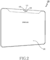
- FIG. 1 and FIG. 2 are respectively front and rear perspective views of an electronic device having a case frame according to an embodiment of the present disclosure.
- a front case frame 110 and a rear case frame 120 are joined to form an outer appearance of an electronic device 100.
- a plurality of electronic components having different functions such as a circuit board, may be placed in an inner space formed by the front case frame 110 and the rear care frame 120.
- a mobile pad or a tablet Personal Computer is illustrated as the electronic device 100 in the figures. However, this is merely an example and not to be construed as limiting.
- a display unit 111 is coupled to the front case frame 110 in an exposed manner.
- a sensor 114 and a main microphone unit 112 may be coupled to an upper portion of the display unit 111.
- An example of the sensor 114 may be an ambient-light sensor for automatically controlling illumination of the display unit 111 by sensing an ambient light beam.
- a camera module 115 for video telephony may be coupled to one side of the ambient-light sensor.
- another camera module 121 for capturing a subject of a photograph may be coupled to an upper portion of the rear case frame 120 of the electronic device 100. Further, a sub microphone unit 123 and a Light Emitting Diode (LED) module 122 may be included to attenuate noise of the main microphone unit 112.
- LED Light Emitting Diode
- the present disclosure is not limited thereto, and thus various additional units may also be provided to perform additional functions of the electronic device 100 in addition to the aforementioned various sensors 114 and camera modules 115 and 121.
- a speaker unit 113 may be coupled to a lateral portion of the electronic device 100 to provide a voice output of a peer user for voice communication or to provide an output of music, voice, sound, etc., of a multimedia file reproduced by the electronic device 100.
- the outer appearance of the front case frame 110 and the rear case frame 120 can be implemented by a manufacturing method of the present disclosure, except for a portion in which peripheral devices are exposed, such as the display unit 111, the microphone units 112 and 123, the camera modules 115 and 121, the LED module 122, or the like of the electronic device 100.
- the electronic device 100 has a built-in battery pack, it is also possible to use an additional battery cover (not shown) to protect a battery pack disposed inside the electronic device 100 in an attachable/detachable manner.
- the battery cover can also be implemented by the frame case manufacturing method of the present disclosure.
- the electronic device 100 of the present disclosure can provide a ceramic pearl texture by reproducing a brightness and a color anisotropy according to a viewing angle of a user, so that the electronic device can have high quality in general.
- the outer appearance of the electronic device can be improved.
- FIG. 3 is a flowchart illustrating a process of manufacturing a case frame according to an embodiment of the present disclosure
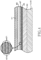
- FIG. 4 is a cross-sectional view illustrating elements of a case frame according to an embodiment of the present disclosure.
- a process of producing a mold for forming the front case frame 110 and the rear case frame 120 having a specific shape according to a design of the electronic device 100 For example, in order to represent a texture of a natural material (e.g., a leaf, etc.) on a surface of a material of the front case frame 110 and the rear case frame 120, an injection surface of a mold for injecting an outer surface of the front case frame 110 and the rear case frame 120 can be produced by performing an etching process several times. For example, a film having a shape depending on the texture of the natural material is produced, and an injection surface of a mold can be etched several times by using the film so that various patterns of the natural material are formed on the surface thereof.
- a natural material e.g., a leaf, etc.
- the front case frame 110 and the rear case frame 120 made of a synthetic resin are injected by the mold formed as described above in operation 301.
- a first painting process i.e., a primer-painting process
- a basis color painting layer 403 of FIG. 4 by painting a basis color corresponding to the natural material.
- a first transparent layer 405 of FIG. 4 is coated on an upper portion of the basis color painting layer 403 of the front case frame 110 and the rear case frame 120.
- the first transparent layer 405 can be formed by spray-painting an SiO 2 -seires solvent such as a glass component or an acrylic-series urethane.
- the present disclosure is not limited thereto, and thus can be formed to have a thickness in the range of 10 ⁇ 20 ⁇ m also by using a transparent urethane paint.
- the first transparent layer 405 serves to uniformly and smoothly coat and fix a deposition material onto the front case frame 110 and the rear case frame 120.
- the front case frame 110 and the rear case frame 120 coated with the first transparent layer 405 can be dried by using an oven or a natural drying process.
- an oxide deposition layer 407 of FIG. 4 is formed in such a manner that deposition materials having different refraction indices are alternately deposited several times on an upper portion of the first transparent layer 405.
- the oxide deposition material is deposited repetitively 3 to 10 times, and thus the deposition materials having different refractive indices can reproduce a different brightness and a color anisotropy according to a viewing angle of a user.
- the oxide deposition layer 407 is preferably formed to have a thickness in the range of 0.05 ⁇ 0.3 ⁇ m.
- two materials selected from a silicon oxide layer (i.e., SiO 2 ), a titanium oxide layer (i.e., TiO 2 ), an aluminum oxide layer (i.e., Al 2 O 3 ), a zirconium oxide layer (i.e., ZrO 2 ), and a tantalum oxide layer (i.e., Ta 2 O 5 ) can be alternately deposited on the transparent oxide deposition layer 407.
- the deposition layer can be formed by alternating the deposition materials formed with SiO 2 -TiO 2 , Al 2 O 3 -TiO 2 , SiO 2 -ZrO 2 , Al 2 O 3 -ZrO 2 , SiO 2 -T a 2O 5 , etc.
- deposition can be achieved by alternating at least two types of deposition materials.
- the at least two types of deposition materials can be mixed to form a first deposition material 4071 having a desired first refraction index and a second deposition material 4072 having a desired second refraction index different from the first refraction index, and the two deposition materials can be alternately deposited.
- a refraction index of SiO 2 is 1.4
- a refraction index of TiO 2 is 2.4
- a refraction index of Al 2 O 3 is 1.7. Therefore, since a refraction index difference is great between the SiO 2 and the TiO 2 , these layers can be alternately deposited on an upper portion of the aforementioned basis color painting layer, which may achieve a ceramic pearl texture effect and a color anisotropy reproduction.
- the oxide deposition layer 407 can be deposited by using an Electron (E)-beam deposition machine for depositing a transparent layer.
- E Electron
- the present disclosure is not limited thereto, and thus various well-known deposition manufacturing processes can be applied.
- a second transparent layer 409 is coated on an upper portion of the oxide deposition layer 407.
- the second transparent layer 409 can protect the oxide deposition layer 407 and the basis color painting layer 403 from an external environment even if a second painting layer 411 to be described below is damaged.
- the second transparent layer 409 can also be used by spraying-painting a transparent urethane paint having a specific luster.
- the second transparent layer can be formed to have a thickness in the range of 10 ⁇ 30 ⁇ m.
- the second painting layer 411 is formed.
- the second painting layer 411 is formed by painting a well-known Soft Feel (SF) paint to naturally represent a color of the basis color painting layer 403 and to produce a smooth natural texture such as a leather or a grain of wood.
- SF Soft Feel
- the SF paint may be a urethane paint which characteristically has a soft touch feel and a leather-like outer appearance, and is advantageous in terms of humidity resistance, solvent resistance, chemical resistance, abrasion resistance, and the like.
- the SF paint is classified into an SF series characterized as having a smooth touch feel and outer appearance, an SF-HJ series used for products designated for the use of a hardly adhesive material, an SF-5 series for maximizing a rubber feel, an SF-6 series for maximizing a slip feel, etc. Accordingly, it is preferable to use an SF paint corresponding to a pattern characteristic of a natural material to be applied.
- the second painting layer 411 depending on the SF paint, can be formed to have a thickness in the range of 10 ⁇ 45 ⁇ m.
- the first painting layer 403 and the oxide deposition layer 407 of the present disclosure are also applicable not only to an injection material based on a mold of a synthetic resin material but also to a case frame made of a metal material such as stainless steel, aluminum, magnesium, etc., formed by a process of pressing, die-casting, or the like.
- a case frame can have an excellent texture by reproducing a brightness and a color anisotropy on the basis of a viewing angle by adding only a simple manufacturing process. Therefore, the electronic device has high quality in general, and a user's desire for purchasing the device can be promoted.
Landscapes
- Chemical & Material Sciences (AREA)
- Engineering & Computer Science (AREA)
- Organic Chemistry (AREA)
- Materials Engineering (AREA)
- Mechanical Engineering (AREA)
- Metallurgy (AREA)
- Chemical Kinetics & Catalysis (AREA)
- Health & Medical Sciences (AREA)
- Toxicology (AREA)
- Ceramic Engineering (AREA)
- Microelectronics & Electronic Packaging (AREA)
- Casings For Electric Apparatus (AREA)
- Physical Vapour Deposition (AREA)
- Laminated Bodies (AREA)
- Telephone Set Structure (AREA)
Claims (12)
- Verfahren des Herstellens eines Gehäuserahmens (110, 120), wobei das Verfahren Folgendes umfasst:Bilden des Gehäuserahmens (110, 120);Bilden einer ersten Lackierschicht (403) mit einer Farbe eines Materials, aufgebracht auf eine Oberfläche des gebildeten Gehäuserahmens (110, 120);Auftragen einer transparenten Oxid-Auftragungsschicht (407), die einen Brechungsindex aufweist, auf einem oberen Abschnitt der ersten Lackierschicht (403) undBilden einer zweiten Lackierschicht (411) auf einem oberen Abschnitt der transparenten Oxid-Auftragungsschicht (407);wobei das Auftragen der Oxid-Auftragungsschicht mehrmalige abwechselnde Auftragung von mindestens zwei unterschiedlichen Arten von Auftragungsmaterialien umfasst und wobei das Auftragen der Oxid-Auftragungsschicht Folgendes beinhaltet:Auftragen eines ersten Auftragungsmaterials, das einen ersten Brechungsindex aufweist und durch mindestens zwei Arten von Gemischen gebildet ist, die aus SiO2-TiO2, Al2O3-TiO2, SiO2-ZrO2, Al2O3-ZrO2 und SiO2-Ta2O5 ausgewählt sind; undAuftragen eines zweiten Auftragungsmaterials, das einen zweiten Brechungsindex aufweist und durch mindestens zwei Arten von Gemischen gebildet ist, die aus SiO2-TiO2, Al2O3-TiO2, SiO2-ZrO2, Al2O3-ZrO2 und SiO2-Ta2O5 ausgewählt sind,wobei Auftragung durch mehrmalige abwechselnde Auftragung des ersten Auftragungsmaterials und des zweiten Auftragungsmaterials erreicht wird und wobei der erste Brechungsindex vom zweiten Brechungsindex verschieden ist.
- Verfahren nach Anspruch 1, wobei die Oxid-Auftragungsschicht in derartiger Art und Weise gebildet wird, dass die mindestens zwei Arten von Auftragungsmaterialien im Bereich von 3 bis 10 Schichten aufgetragen werden.
- Verfahren nach Anspruch 1, wobei die Oxid-Auftragungsschicht so gebildet wird, dass sie eine Dicke im Bereich von 0,05-0,3 µm aufweist.
- Verfahren nach Anspruch 1, wobei die Oxid-Auftragungsschicht unter Verwendung einer Elektronenstrahl-Auftragungsmaschine (E-Beam-Auftragungsmaschine) aufgetragen wird.
- Verfahren nach Anspruch 1, das ferner Bilden einer ersten transparenten Schicht zwischen der ersten Lackierschicht und der transparenten Oxid-Auftragung, die eine bestimmte Dicke aufweist, nach dem Bilden der ersten Lackierschicht umfasst.
- Verfahren nach Anspruch 5, wobei die erste transparente Schicht unter Verwendung eines transparenten Urethanlacks so gebildet wird, dass sie eine Dicke im Bereich von 10-20 µm aufweist.
- Verfahren nach Anspruch 1, wobei die erste Lackierschicht und die Oxid-Auftragungsschicht so gebildet werden, dass sie eine Gesamtdicke im Bereich von 20-150 µm aufweisen.
- Verfahren nach Anspruch 1, das ferner Bilden einer zweiten transparenten Schicht, die auf der transparenten Oxid-Auftragungsschicht aufgetragen wird, die eine bestimmte Dicke aufweist, nach dem Bilden der Oxid-Auftragungsschicht umfasst.
- Verfahren nach Anspruch 8, wobei die zweite transparente Schicht unter Verwendung eines transparenten Urethanlacks so gebildet wird, dass sie eine Dicke im Bereich von 10-30 µm aufweist.
- Verfahren nach Anspruch 1, wobei der Gehäuserahmen aus einem Metallwerkstoff hergestellt wird und durch mindestens eines von Pressen und Druckgießen gebildet wird.
- Verfahren nach Anspruch 10, wobei der Gehäuserahmen aus mindestens einem von rostfreiem Stahl, Aluminium, Magnesium und Kupfer hergestellt wird.
- Elektronisches Gerät (100), wobei das Gerät Folgendes umfasst:mindestens ein elektronisches Bauteil undeinen Gehäuserahmen (110, 120), der von einer Gestalt ist, die dem elektronischen Gerät (100) entspricht, das das mindestens eine elektronische Bauteil beinhaltet, wobei der Gehäuserahmen (110, 120) Folgendes umfasst:eine erste Lackierschicht (403) mit einer Farbe eines Materials, aufgebracht auf eine Oberfläche des gebildeten Gehäuserahmens (110, 120);eine transparente Oxid-Auftragungsschicht (407), die einen Brechungsindex aufweist, auf einem oberen Abschnitt der ersten Lackierschicht (403) undeine zweite Lackierschicht (411) auf einem oberen Abschnitt der transparenten Oxid-Auftragungsschicht (407),wobei das Auftragen der Oxid-Auftragungsschicht mehrmalige abwechselnde Auftragung von mindestens zwei unterschiedlichen Arten von Auftragungsmaterialien umfasst und wobei das Auftragen der Oxid-Auftragungsschicht Folgendes beinhaltet:Auftragen eines ersten Auftragungsmaterials, das einen ersten Brechungsindex aufweist und durch mindestens zwei Arten von Gemischen gebildet ist, die aus SiO2-TiO2, Al2O3-TiO2, SiO2-ZrO2, Al2O3-ZrO2 und SiO2-Ta2O5 ausgewählt sind; undAuftragen eines zweiten Auftragungsmaterials, das einen zweiten Brechungsindex aufweist und durch mindestens zwei Arten von Gemischen gebildet ist, die aus SiO2-TiO2, Al2O3-TiO2, SiO2-ZrO2, Al2O3-ZrO2 und SiO2-Ta2O5 ausgewählt sind,wobei Auftragung durch mehrmalige abwechselnde Auftragung des ersten Auftragungsmaterials und des zweiten Auftragungsmaterials erreicht wird und wobei der erste Brechungsindex vom zweiten Brechungsindex verschieden ist.
Applications Claiming Priority (1)
| Application Number | Priority Date | Filing Date | Title |
|---|---|---|---|
| KR1020120122890A KR102051583B1 (ko) | 2012-11-01 | 2012-11-01 | 케이스 프레임 및 그 제조 방법 |
Publications (2)
| Publication Number | Publication Date |
|---|---|
| EP2728037A1 EP2728037A1 (de) | 2014-05-07 |
| EP2728037B1 true EP2728037B1 (de) | 2017-08-09 |
Family
ID=49510079
Family Applications (1)
| Application Number | Title | Priority Date | Filing Date |
|---|---|---|---|
| EP13191267.7A Not-in-force EP2728037B1 (de) | 2012-11-01 | 2013-11-01 | Gehäuserahmen und Herstellungsverfahren dafür |
Country Status (7)
| Country | Link |
|---|---|
| US (1) | US9867298B2 (de) |
| EP (1) | EP2728037B1 (de) |
| JP (1) | JP5753559B2 (de) |
| KR (1) | KR102051583B1 (de) |
| CN (1) | CN103802577A (de) |
| AU (1) | AU2013213693B2 (de) |
| WO (1) | WO2014069760A1 (de) |
Families Citing this family (17)
| Publication number | Priority date | Publication date | Assignee | Title |
|---|---|---|---|---|
| USD741269S1 (en) * | 2014-07-15 | 2015-10-20 | Vivint, Inc. | Touch panel |
| CN105451483A (zh) * | 2014-08-28 | 2016-03-30 | 深圳富泰宏精密工业有限公司 | 壳体及具有该壳体的电子装置 |
| KR102411372B1 (ko) * | 2015-01-30 | 2022-06-22 | 삼성전자주식회사 | 하우징, 하우징 제조 방법 및 그것을 포함하는 전자 장치 |
| KR102398581B1 (ko) * | 2015-04-21 | 2022-05-17 | 삼성전자주식회사 | 하우징, 하우징 제조 방법 및 그것을 포함하는 전자 장치 |
| KR20180088157A (ko) * | 2017-01-26 | 2018-08-03 | 삼성전자주식회사 | 하우징, 하우징 제조 방법 및 그것을 포함하는 전자 장치 |
| US10399905B2 (en) | 2017-08-31 | 2019-09-03 | Corning Incorporated | Ceramic housing with texture |
| CN107899920A (zh) * | 2017-10-30 | 2018-04-13 | 广东欧珀移动通信有限公司 | 壳体制作方法、壳体及电子设备 |
| KR102462030B1 (ko) * | 2018-06-14 | 2022-11-01 | 인테벡, 인코포레이티드 | 멀티 칼라 절연 코팅 및 uv 잉크젯 프린팅 |
| CN109067939A (zh) * | 2018-06-28 | 2018-12-21 | Oppo广东移动通信有限公司 | 电子设备的壳体及其制作方法、电子设备 |
| CN109348660B (zh) * | 2018-11-16 | 2022-08-19 | 昇印光电(昆山)股份有限公司 | 装饰片及消费电子产品盖板 |
| KR102406233B1 (ko) * | 2018-12-19 | 2022-06-08 | 삼성전자 주식회사 | 데코레이션 필름 및 이를 포함하는 전자장치 |
| CN110624805A (zh) * | 2019-09-17 | 2019-12-31 | 苏州兴禾源复合材料有限公司 | 具有拉丝变色效果的透明pcm彩涂板 |
| CN110586430B (zh) * | 2019-09-17 | 2022-04-01 | 苏州兴禾源复合材料有限公司 | 具有变色效果的pcm彩涂板 |
| KR20210043110A (ko) * | 2019-10-11 | 2021-04-21 | 삼성전자주식회사 | 하우징 및 이를 포함하는 전자 장치 |
| CN110747432A (zh) * | 2019-11-28 | 2020-02-04 | 维沃移动通信有限公司 | 电子设备、电子设备的壳体及其加工方法 |
| CN111683484B (zh) * | 2020-06-28 | 2021-11-05 | 江西沃格光电股份有限公司 | 有色基板及其制作方法及电子设备的外壳 |
| CN112297538B (zh) * | 2020-10-28 | 2023-05-26 | Oppo广东移动通信有限公司 | 仿陶瓷壳体及其制备方法和电子设备 |
Family Cites Families (20)
| Publication number | Priority date | Publication date | Assignee | Title |
|---|---|---|---|---|
| JPH1020102A (ja) * | 1996-07-03 | 1998-01-23 | Nikon Corp | 反射防止膜 |
| JP4538720B2 (ja) | 2004-04-13 | 2010-09-08 | 株式会社フクダコーポレーション | 樹脂基材又は金属基材の加飾方法 |
| US20060024493A1 (en) | 2004-07-28 | 2006-02-02 | Jones R P | Color effect/soft feel coating |
| CN100490615C (zh) * | 2005-03-25 | 2009-05-20 | 鸿富锦精密工业(深圳)有限公司 | 便携式电子装置外壳 |
| KR100744399B1 (ko) | 2005-12-21 | 2007-07-30 | 삼성전자주식회사 | 휴대 단말기 및 전자기기의 표면에 사용되는 질감 도료용도료 조성물 및 제조방법 |
| US7688574B2 (en) | 2007-01-05 | 2010-03-30 | Apple Inc. | Cold worked metal housing for a portable electronic device |
| KR101452481B1 (ko) | 2007-06-19 | 2014-10-23 | 삼성전자주식회사 | 휴대용 전자 장치의 외관 도장 방법 |
| WO2009008403A1 (ja) | 2007-07-11 | 2009-01-15 | Nissha Printing Co., Ltd. | 筐体用加飾板及び筐体 |
| CN101417863B (zh) | 2007-10-25 | 2011-08-24 | 鸿富锦精密工业(深圳)有限公司 | 壳体及表面处理方法 |
| KR20090051831A (ko) | 2007-11-20 | 2009-05-25 | 주식회사 삼광 | 광학 코팅된 휴대폰 표시창용 케이스의 제조방법 |
| CN102098887B (zh) | 2009-12-14 | 2013-08-07 | 深圳富泰宏精密工业有限公司 | 电子装置壳体 |
| CN102111969A (zh) * | 2009-12-25 | 2011-06-29 | 深圳富泰宏精密工业有限公司 | 电子装置壳体 |
| CN102111971B (zh) * | 2009-12-29 | 2013-07-03 | 深圳富泰宏精密工业有限公司 | 电子装置壳体 |
| CN102111972B (zh) * | 2009-12-29 | 2015-07-29 | 深圳富泰宏精密工业有限公司 | 电子装置壳体 |
| CN102223771B (zh) * | 2010-04-14 | 2015-04-15 | 深圳富泰宏精密工业有限公司 | 电子装置壳体及其制作方法 |
| JP5710170B2 (ja) | 2010-07-30 | 2015-04-30 | 株式会社ニデック | 加飾体、及び加飾体の製造方法 |
| US20120084884A1 (en) | 2010-10-05 | 2012-04-05 | University Of Tennessee Research Foundation | Stably transformed ferns and related methods |
| CN102448261A (zh) | 2010-10-11 | 2012-05-09 | 深圳富泰宏精密工业有限公司 | 电子装置外壳及其制造方法 |
| CN102605325B (zh) * | 2011-01-22 | 2015-03-25 | 深圳富泰宏精密工业有限公司 | 电子装置壳体及其制作方法 |
| CN103369878A (zh) * | 2012-03-29 | 2013-10-23 | 深圳富泰宏精密工业有限公司 | 电子装置壳体及其制造方法 |
-
2012
- 2012-11-01 KR KR1020120122890A patent/KR102051583B1/ko not_active Expired - Fee Related
-
2013
- 2013-08-06 US US13/960,175 patent/US9867298B2/en not_active Expired - Fee Related
- 2013-08-07 WO PCT/KR2013/007128 patent/WO2014069760A1/en not_active Ceased
- 2013-08-07 AU AU2013213693A patent/AU2013213693B2/en not_active Ceased
- 2013-08-16 JP JP2013169085A patent/JP5753559B2/ja not_active Expired - Fee Related
- 2013-10-12 CN CN201310475902.6A patent/CN103802577A/zh active Pending
- 2013-11-01 EP EP13191267.7A patent/EP2728037B1/de not_active Not-in-force
Non-Patent Citations (1)
| Title |
|---|
| None * |
Also Published As
| Publication number | Publication date |
|---|---|
| WO2014069760A1 (en) | 2014-05-08 |
| JP2014091864A (ja) | 2014-05-19 |
| KR102051583B1 (ko) | 2019-12-03 |
| AU2013213693B2 (en) | 2016-01-07 |
| AU2013213693A1 (en) | 2014-05-15 |
| CN103802577A (zh) | 2014-05-21 |
| US9867298B2 (en) | 2018-01-09 |
| EP2728037A1 (de) | 2014-05-07 |
| KR20140055690A (ko) | 2014-05-09 |
| JP5753559B2 (ja) | 2015-07-22 |
| US20140118903A1 (en) | 2014-05-01 |
Similar Documents
| Publication | Publication Date | Title |
|---|---|---|
| US9867298B2 (en) | Case frame and manufacturing method thereof | |
| CN106064545B (zh) | 壳体、制造壳体的方法以及包括壳体的电子设备 | |
| CN102111971B (zh) | 电子装置壳体 | |
| US9462093B2 (en) | Method and apparatus for personalizing consumer products | |
| CN111010838B (zh) | 壳体的制造方法、壳体以及电子设备 | |
| CN113614672B (zh) | 包括后板的电子装置及其制造方法 | |
| EP3880471B1 (de) | Zierfolie und elektronische vorrichtung damit | |
| US20100035005A1 (en) | Housing and manufacturing method thereof | |
| JP2008254428A (ja) | 携帯電子装置用カバー及びその製造方法 | |
| US20090239068A1 (en) | Housing for mobile devices | |
| CN108263141A (zh) | 板材及其制备方法、壳体、电子设备 | |
| US20130257241A1 (en) | Method for manufacturing case frame and an electronic device employing thereof | |
| KR20140128150A (ko) | 이동 단말기 및 이에 구비되는 케이스의 제조 방법 | |
| CN113568282A (zh) | 转印模具的制备方法、壳体组件及其制备方法、电子设备 | |
| KR20140057127A (ko) | 휴대용 단말기의 윈도우 부재 및 그 제작 방법 | |
| CN112848563B (zh) | 玻璃壳体及其制造方法、电子设备 | |
| JP2011096992A (ja) | 蓋体及びその製造方法 | |
| CN101841983A (zh) | 设备壳体及其制造方法、以及设备 | |
| EP3041383B1 (de) | Abdeckungselement und verfahren zur herstellung davon | |
| CN110868819A (zh) | 壳体的制备方法、壳体和电子设备 | |
| CN216356797U (zh) | 手机后盖、壳体及电子设备 | |
| KR101317249B1 (ko) | 지문인식센서와 사출물 간의 밀착력이 향상된 구조를 갖는 지문인식 홈키 제조방법 및 지문인식 홈키 | |
| CN216411615U (zh) | 渐变炫彩膜和保护壳 | |
| CN115623709B (zh) | 电子设备、分色结构件及其制备方法 | |
| CN108828869A (zh) | 电致变色结构及其制作方法、电子设备 |
Legal Events
| Date | Code | Title | Description |
|---|---|---|---|
| PUAI | Public reference made under article 153(3) epc to a published international application that has entered the european phase |
Free format text: ORIGINAL CODE: 0009012 |
|
| 17P | Request for examination filed |
Effective date: 20131101 |
|
| AK | Designated contracting states |
Kind code of ref document: A1 Designated state(s): AL AT BE BG CH CY CZ DE DK EE ES FI FR GB GR HR HU IE IS IT LI LT LU LV MC MK MT NL NO PL PT RO RS SE SI SK SM TR |
|
| AX | Request for extension of the european patent |
Extension state: BA ME |
|
| 17Q | First examination report despatched |
Effective date: 20150917 |
|
| GRAP | Despatch of communication of intention to grant a patent |
Free format text: ORIGINAL CODE: EPIDOSNIGR1 |
|
| INTG | Intention to grant announced |
Effective date: 20170302 |
|
| GRAS | Grant fee paid |
Free format text: ORIGINAL CODE: EPIDOSNIGR3 |
|
| GRAA | (expected) grant |
Free format text: ORIGINAL CODE: 0009210 |
|
| AK | Designated contracting states |
Kind code of ref document: B1 Designated state(s): AL AT BE BG CH CY CZ DE DK EE ES FI FR GB GR HR HU IE IS IT LI LT LU LV MC MK MT NL NO PL PT RO RS SE SI SK SM TR |
|
| REG | Reference to a national code |
Ref country code: GB Ref legal event code: FG4D |
|
| REG | Reference to a national code |
Ref country code: CH Ref legal event code: EP Ref country code: AT Ref legal event code: REF Ref document number: 916940 Country of ref document: AT Kind code of ref document: T Effective date: 20170815 |
|
| REG | Reference to a national code |
Ref country code: IE Ref legal event code: FG4D |
|
| REG | Reference to a national code |
Ref country code: DE Ref legal event code: R096 Ref document number: 602013024677 Country of ref document: DE |
|
| REG | Reference to a national code |
Ref country code: NL Ref legal event code: MP Effective date: 20170809 |
|
| REG | Reference to a national code |
Ref country code: LT Ref legal event code: MG4D |
|
| REG | Reference to a national code |
Ref country code: AT Ref legal event code: MK05 Ref document number: 916940 Country of ref document: AT Kind code of ref document: T Effective date: 20170809 |
|
| PG25 | Lapsed in a contracting state [announced via postgrant information from national office to epo] |
Ref country code: SE Free format text: LAPSE BECAUSE OF FAILURE TO SUBMIT A TRANSLATION OF THE DESCRIPTION OR TO PAY THE FEE WITHIN THE PRESCRIBED TIME-LIMIT Effective date: 20170809 Ref country code: NO Free format text: LAPSE BECAUSE OF FAILURE TO SUBMIT A TRANSLATION OF THE DESCRIPTION OR TO PAY THE FEE WITHIN THE PRESCRIBED TIME-LIMIT Effective date: 20171109 Ref country code: FI Free format text: LAPSE BECAUSE OF FAILURE TO SUBMIT A TRANSLATION OF THE DESCRIPTION OR TO PAY THE FEE WITHIN THE PRESCRIBED TIME-LIMIT Effective date: 20170809 Ref country code: NL Free format text: LAPSE BECAUSE OF FAILURE TO SUBMIT A TRANSLATION OF THE DESCRIPTION OR TO PAY THE FEE WITHIN THE PRESCRIBED TIME-LIMIT Effective date: 20170809 Ref country code: LT Free format text: LAPSE BECAUSE OF FAILURE TO SUBMIT A TRANSLATION OF THE DESCRIPTION OR TO PAY THE FEE WITHIN THE PRESCRIBED TIME-LIMIT Effective date: 20170809 Ref country code: HR Free format text: LAPSE BECAUSE OF FAILURE TO SUBMIT A TRANSLATION OF THE DESCRIPTION OR TO PAY THE FEE WITHIN THE PRESCRIBED TIME-LIMIT Effective date: 20170809 Ref country code: AT Free format text: LAPSE BECAUSE OF FAILURE TO SUBMIT A TRANSLATION OF THE DESCRIPTION OR TO PAY THE FEE WITHIN THE PRESCRIBED TIME-LIMIT Effective date: 20170809 |
|
| PGFP | Annual fee paid to national office [announced via postgrant information from national office to epo] |
Ref country code: DE Payment date: 20171128 Year of fee payment: 5 |
|
| PG25 | Lapsed in a contracting state [announced via postgrant information from national office to epo] |
Ref country code: IS Free format text: LAPSE BECAUSE OF FAILURE TO SUBMIT A TRANSLATION OF THE DESCRIPTION OR TO PAY THE FEE WITHIN THE PRESCRIBED TIME-LIMIT Effective date: 20171209 Ref country code: ES Free format text: LAPSE BECAUSE OF FAILURE TO SUBMIT A TRANSLATION OF THE DESCRIPTION OR TO PAY THE FEE WITHIN THE PRESCRIBED TIME-LIMIT Effective date: 20170809 Ref country code: LV Free format text: LAPSE BECAUSE OF FAILURE TO SUBMIT A TRANSLATION OF THE DESCRIPTION OR TO PAY THE FEE WITHIN THE PRESCRIBED TIME-LIMIT Effective date: 20170809 Ref country code: RS Free format text: LAPSE BECAUSE OF FAILURE TO SUBMIT A TRANSLATION OF THE DESCRIPTION OR TO PAY THE FEE WITHIN THE PRESCRIBED TIME-LIMIT Effective date: 20170809 Ref country code: BG Free format text: LAPSE BECAUSE OF FAILURE TO SUBMIT A TRANSLATION OF THE DESCRIPTION OR TO PAY THE FEE WITHIN THE PRESCRIBED TIME-LIMIT Effective date: 20171109 Ref country code: PL Free format text: LAPSE BECAUSE OF FAILURE TO SUBMIT A TRANSLATION OF THE DESCRIPTION OR TO PAY THE FEE WITHIN THE PRESCRIBED TIME-LIMIT Effective date: 20170809 Ref country code: GR Free format text: LAPSE BECAUSE OF FAILURE TO SUBMIT A TRANSLATION OF THE DESCRIPTION OR TO PAY THE FEE WITHIN THE PRESCRIBED TIME-LIMIT Effective date: 20171110 |
|
| PGFP | Annual fee paid to national office [announced via postgrant information from national office to epo] |
Ref country code: GB Payment date: 20171031 Year of fee payment: 5 |
|
| PG25 | Lapsed in a contracting state [announced via postgrant information from national office to epo] |
Ref country code: DK Free format text: LAPSE BECAUSE OF FAILURE TO SUBMIT A TRANSLATION OF THE DESCRIPTION OR TO PAY THE FEE WITHIN THE PRESCRIBED TIME-LIMIT Effective date: 20170809 Ref country code: CZ Free format text: LAPSE BECAUSE OF FAILURE TO SUBMIT A TRANSLATION OF THE DESCRIPTION OR TO PAY THE FEE WITHIN THE PRESCRIBED TIME-LIMIT Effective date: 20170809 Ref country code: RO Free format text: LAPSE BECAUSE OF FAILURE TO SUBMIT A TRANSLATION OF THE DESCRIPTION OR TO PAY THE FEE WITHIN THE PRESCRIBED TIME-LIMIT Effective date: 20170809 |
|
| REG | Reference to a national code |
Ref country code: DE Ref legal event code: R097 Ref document number: 602013024677 Country of ref document: DE |
|
| PG25 | Lapsed in a contracting state [announced via postgrant information from national office to epo] |
Ref country code: IT Free format text: LAPSE BECAUSE OF FAILURE TO SUBMIT A TRANSLATION OF THE DESCRIPTION OR TO PAY THE FEE WITHIN THE PRESCRIBED TIME-LIMIT Effective date: 20170809 Ref country code: SK Free format text: LAPSE BECAUSE OF FAILURE TO SUBMIT A TRANSLATION OF THE DESCRIPTION OR TO PAY THE FEE WITHIN THE PRESCRIBED TIME-LIMIT Effective date: 20170809 Ref country code: EE Free format text: LAPSE BECAUSE OF FAILURE TO SUBMIT A TRANSLATION OF THE DESCRIPTION OR TO PAY THE FEE WITHIN THE PRESCRIBED TIME-LIMIT Effective date: 20170809 Ref country code: SM Free format text: LAPSE BECAUSE OF FAILURE TO SUBMIT A TRANSLATION OF THE DESCRIPTION OR TO PAY THE FEE WITHIN THE PRESCRIBED TIME-LIMIT Effective date: 20170809 |
|
| PLBE | No opposition filed within time limit |
Free format text: ORIGINAL CODE: 0009261 |
|
| STAA | Information on the status of an ep patent application or granted ep patent |
Free format text: STATUS: NO OPPOSITION FILED WITHIN TIME LIMIT |
|
| PG25 | Lapsed in a contracting state [announced via postgrant information from national office to epo] |
Ref country code: MC Free format text: LAPSE BECAUSE OF FAILURE TO SUBMIT A TRANSLATION OF THE DESCRIPTION OR TO PAY THE FEE WITHIN THE PRESCRIBED TIME-LIMIT Effective date: 20170809 |
|
| 26N | No opposition filed |
Effective date: 20180511 |
|
| PG25 | Lapsed in a contracting state [announced via postgrant information from national office to epo] |
Ref country code: CH Free format text: LAPSE BECAUSE OF NON-PAYMENT OF DUE FEES Effective date: 20171130 Ref country code: LI Free format text: LAPSE BECAUSE OF NON-PAYMENT OF DUE FEES Effective date: 20171130 |
|
| PG25 | Lapsed in a contracting state [announced via postgrant information from national office to epo] |
Ref country code: SI Free format text: LAPSE BECAUSE OF FAILURE TO SUBMIT A TRANSLATION OF THE DESCRIPTION OR TO PAY THE FEE WITHIN THE PRESCRIBED TIME-LIMIT Effective date: 20170809 Ref country code: LU Free format text: LAPSE BECAUSE OF NON-PAYMENT OF DUE FEES Effective date: 20171101 |
|
| REG | Reference to a national code |
Ref country code: FR Ref legal event code: ST Effective date: 20180731 Ref country code: BE Ref legal event code: MM Effective date: 20171130 |
|
| REG | Reference to a national code |
Ref country code: IE Ref legal event code: MM4A |
|
| PG25 | Lapsed in a contracting state [announced via postgrant information from national office to epo] |
Ref country code: MT Free format text: LAPSE BECAUSE OF NON-PAYMENT OF DUE FEES Effective date: 20171101 |
|
| PG25 | Lapsed in a contracting state [announced via postgrant information from national office to epo] |
Ref country code: FR Free format text: LAPSE BECAUSE OF NON-PAYMENT OF DUE FEES Effective date: 20171130 Ref country code: IE Free format text: LAPSE BECAUSE OF NON-PAYMENT OF DUE FEES Effective date: 20171101 |
|
| PG25 | Lapsed in a contracting state [announced via postgrant information from national office to epo] |
Ref country code: BE Free format text: LAPSE BECAUSE OF NON-PAYMENT OF DUE FEES Effective date: 20171130 |
|
| REG | Reference to a national code |
Ref country code: DE Ref legal event code: R119 Ref document number: 602013024677 Country of ref document: DE |
|
| PG25 | Lapsed in a contracting state [announced via postgrant information from national office to epo] |
Ref country code: HU Free format text: LAPSE BECAUSE OF FAILURE TO SUBMIT A TRANSLATION OF THE DESCRIPTION OR TO PAY THE FEE WITHIN THE PRESCRIBED TIME-LIMIT; INVALID AB INITIO Effective date: 20131101 |
|
| GBPC | Gb: european patent ceased through non-payment of renewal fee |
Effective date: 20181101 |
|
| PG25 | Lapsed in a contracting state [announced via postgrant information from national office to epo] |
Ref country code: DE Free format text: LAPSE BECAUSE OF NON-PAYMENT OF DUE FEES Effective date: 20190601 Ref country code: CY Free format text: LAPSE BECAUSE OF NON-PAYMENT OF DUE FEES Effective date: 20170809 |
|
| PG25 | Lapsed in a contracting state [announced via postgrant information from national office to epo] |
Ref country code: MK Free format text: LAPSE BECAUSE OF FAILURE TO SUBMIT A TRANSLATION OF THE DESCRIPTION OR TO PAY THE FEE WITHIN THE PRESCRIBED TIME-LIMIT Effective date: 20170809 |
|
| PG25 | Lapsed in a contracting state [announced via postgrant information from national office to epo] |
Ref country code: GB Free format text: LAPSE BECAUSE OF NON-PAYMENT OF DUE FEES Effective date: 20181101 |
|
| PG25 | Lapsed in a contracting state [announced via postgrant information from national office to epo] |
Ref country code: TR Free format text: LAPSE BECAUSE OF FAILURE TO SUBMIT A TRANSLATION OF THE DESCRIPTION OR TO PAY THE FEE WITHIN THE PRESCRIBED TIME-LIMIT Effective date: 20170809 |
|
| PG25 | Lapsed in a contracting state [announced via postgrant information from national office to epo] |
Ref country code: PT Free format text: LAPSE BECAUSE OF FAILURE TO SUBMIT A TRANSLATION OF THE DESCRIPTION OR TO PAY THE FEE WITHIN THE PRESCRIBED TIME-LIMIT Effective date: 20170809 |
|
| PG25 | Lapsed in a contracting state [announced via postgrant information from national office to epo] |
Ref country code: AL Free format text: LAPSE BECAUSE OF FAILURE TO SUBMIT A TRANSLATION OF THE DESCRIPTION OR TO PAY THE FEE WITHIN THE PRESCRIBED TIME-LIMIT Effective date: 20170809 |