EP2713411B1 - Dispositif de luminescence - Google Patents
Dispositif de luminescence Download PDFInfo
- Publication number
- EP2713411B1 EP2713411B1 EP13185895.3A EP13185895A EP2713411B1 EP 2713411 B1 EP2713411 B1 EP 2713411B1 EP 13185895 A EP13185895 A EP 13185895A EP 2713411 B1 EP2713411 B1 EP 2713411B1
- Authority
- EP
- European Patent Office
- Prior art keywords
- led chip
- luminescence device
- electrode
- disposed
- substrate
- Prior art date
- Legal status (The legal status is an assumption and is not a legal conclusion. Google has not performed a legal analysis and makes no representation as to the accuracy of the status listed.)
- Active
Links
- 238000004020 luminiscence type Methods 0.000 title claims description 51
- OAICVXFJPJFONN-UHFFFAOYSA-N Phosphorus Chemical compound [P] OAICVXFJPJFONN-UHFFFAOYSA-N 0.000 claims description 53
- 239000000758 substrate Substances 0.000 claims description 52
- 239000002184 metal Substances 0.000 claims description 46
- 229910052751 metal Inorganic materials 0.000 claims description 46
- 229910052802 copper Inorganic materials 0.000 claims description 36
- 239000010949 copper Substances 0.000 claims description 36
- RYGMFSIKBFXOCR-UHFFFAOYSA-N Copper Chemical compound [Cu] RYGMFSIKBFXOCR-UHFFFAOYSA-N 0.000 claims description 33
- 239000011800 void material Substances 0.000 claims description 13
- 238000005538 encapsulation Methods 0.000 claims description 12
- 239000011521 glass Substances 0.000 claims description 10
- 239000000853 adhesive Substances 0.000 claims description 7
- 230000001070 adhesive effect Effects 0.000 claims description 7
- 229920005989 resin Polymers 0.000 claims description 6
- 239000011347 resin Substances 0.000 claims description 6
- 229910052737 gold Inorganic materials 0.000 claims description 5
- 229910052709 silver Inorganic materials 0.000 claims description 5
- BPQQTUXANYXVAA-UHFFFAOYSA-N Orthosilicate Chemical compound [O-][Si]([O-])([O-])[O-] BPQQTUXANYXVAA-UHFFFAOYSA-N 0.000 claims description 4
- UCKMPCXJQFINFW-UHFFFAOYSA-N Sulphide Chemical compound [S-2] UCKMPCXJQFINFW-UHFFFAOYSA-N 0.000 claims description 4
- 150000004767 nitrides Chemical class 0.000 claims description 4
- 238000005260 corrosion Methods 0.000 claims description 3
- 239000012774 insulation material Substances 0.000 claims description 3
- 230000001681 protective effect Effects 0.000 claims description 3
- 238000001035 drying Methods 0.000 claims description 2
- 238000010304 firing Methods 0.000 claims description 2
- 239000000463 material Substances 0.000 description 7
- 238000000034 method Methods 0.000 description 5
- 239000000919 ceramic Substances 0.000 description 3
- 238000009792 diffusion process Methods 0.000 description 2
- 239000004065 semiconductor Substances 0.000 description 2
- 239000000956 alloy Substances 0.000 description 1
- 229910045601 alloy Inorganic materials 0.000 description 1
- 229910052782 aluminium Inorganic materials 0.000 description 1
- PNEYBMLMFCGWSK-UHFFFAOYSA-N aluminium oxide Inorganic materials [O-2].[O-2].[O-2].[Al+3].[Al+3] PNEYBMLMFCGWSK-UHFFFAOYSA-N 0.000 description 1
- 230000015556 catabolic process Effects 0.000 description 1
- 229910010293 ceramic material Inorganic materials 0.000 description 1
- 229910052804 chromium Inorganic materials 0.000 description 1
- 229910052593 corundum Inorganic materials 0.000 description 1
- 238000006731 degradation reaction Methods 0.000 description 1
- 230000007613 environmental effect Effects 0.000 description 1
- 239000003822 epoxy resin Substances 0.000 description 1
- 238000005530 etching Methods 0.000 description 1
- 230000004907 flux Effects 0.000 description 1
- 229910052738 indium Inorganic materials 0.000 description 1
- 238000009413 insulation Methods 0.000 description 1
- 229910052745 lead Inorganic materials 0.000 description 1
- 239000004973 liquid crystal related substance Substances 0.000 description 1
- 239000002905 metal composite material Substances 0.000 description 1
- 239000007769 metal material Substances 0.000 description 1
- 229910052750 molybdenum Inorganic materials 0.000 description 1
- 229910052759 nickel Inorganic materials 0.000 description 1
- 229910052697 platinum Inorganic materials 0.000 description 1
- 229920000647 polyepoxide Polymers 0.000 description 1
- 239000002861 polymer material Substances 0.000 description 1
- 230000005855 radiation Effects 0.000 description 1
- 238000011160 research Methods 0.000 description 1
- 230000000452 restraining effect Effects 0.000 description 1
- 229910052702 rhenium Inorganic materials 0.000 description 1
- 229910052707 ruthenium Inorganic materials 0.000 description 1
- 239000002210 silicon-based material Substances 0.000 description 1
- 229920002050 silicone resin Polymers 0.000 description 1
- 238000006467 substitution reaction Methods 0.000 description 1
- 229910052715 tantalum Inorganic materials 0.000 description 1
- 229910052718 tin Inorganic materials 0.000 description 1
- 229910052719 titanium Inorganic materials 0.000 description 1
- 229910052721 tungsten Inorganic materials 0.000 description 1
- 229910001845 yogo sapphire Inorganic materials 0.000 description 1
- 229910052725 zinc Inorganic materials 0.000 description 1
Images

Classifications
-
- H—ELECTRICITY
- H01—ELECTRIC ELEMENTS
- H01L—SEMICONDUCTOR DEVICES NOT COVERED BY CLASS H10
- H01L24/00—Arrangements for connecting or disconnecting semiconductor or solid-state bodies; Methods or apparatus related thereto
- H01L24/01—Means for bonding being attached to, or being formed on, the surface to be connected, e.g. chip-to-package, die-attach, "first-level" interconnects; Manufacturing methods related thereto
- H01L24/02—Bonding areas ; Manufacturing methods related thereto
- H01L24/04—Structure, shape, material or disposition of the bonding areas prior to the connecting process
-
- H—ELECTRICITY
- H01—ELECTRIC ELEMENTS
- H01L—SEMICONDUCTOR DEVICES NOT COVERED BY CLASS H10
- H01L33/00—Semiconductor devices having potential barriers specially adapted for light emission; Processes or apparatus specially adapted for the manufacture or treatment thereof or of parts thereof; Details thereof
- H01L33/48—Semiconductor devices having potential barriers specially adapted for light emission; Processes or apparatus specially adapted for the manufacture or treatment thereof or of parts thereof; Details thereof characterised by the semiconductor body packages
-
- H—ELECTRICITY
- H01—ELECTRIC ELEMENTS
- H01L—SEMICONDUCTOR DEVICES NOT COVERED BY CLASS H10
- H01L24/00—Arrangements for connecting or disconnecting semiconductor or solid-state bodies; Methods or apparatus related thereto
- H01L24/01—Means for bonding being attached to, or being formed on, the surface to be connected, e.g. chip-to-package, die-attach, "first-level" interconnects; Manufacturing methods related thereto
- H01L24/02—Bonding areas ; Manufacturing methods related thereto
- H01L24/04—Structure, shape, material or disposition of the bonding areas prior to the connecting process
- H01L24/05—Structure, shape, material or disposition of the bonding areas prior to the connecting process of an individual bonding area
-
- H—ELECTRICITY
- H01—ELECTRIC ELEMENTS
- H01L—SEMICONDUCTOR DEVICES NOT COVERED BY CLASS H10
- H01L23/00—Details of semiconductor or other solid state devices
- H01L23/48—Arrangements for conducting electric current to or from the solid state body in operation, e.g. leads, terminal arrangements ; Selection of materials therefor
- H01L23/488—Arrangements for conducting electric current to or from the solid state body in operation, e.g. leads, terminal arrangements ; Selection of materials therefor consisting of soldered or bonded constructions
- H01L23/498—Leads, i.e. metallisations or lead-frames on insulating substrates, e.g. chip carriers
- H01L23/49838—Geometry or layout
-
- H—ELECTRICITY
- H01—ELECTRIC ELEMENTS
- H01L—SEMICONDUCTOR DEVICES NOT COVERED BY CLASS H10
- H01L24/00—Arrangements for connecting or disconnecting semiconductor or solid-state bodies; Methods or apparatus related thereto
- H01L24/01—Means for bonding being attached to, or being formed on, the surface to be connected, e.g. chip-to-package, die-attach, "first-level" interconnects; Manufacturing methods related thereto
- H01L24/02—Bonding areas ; Manufacturing methods related thereto
- H01L24/04—Structure, shape, material or disposition of the bonding areas prior to the connecting process
- H01L24/06—Structure, shape, material or disposition of the bonding areas prior to the connecting process of a plurality of bonding areas
-
- H—ELECTRICITY
- H01—ELECTRIC ELEMENTS
- H01L—SEMICONDUCTOR DEVICES NOT COVERED BY CLASS H10
- H01L33/00—Semiconductor devices having potential barriers specially adapted for light emission; Processes or apparatus specially adapted for the manufacture or treatment thereof or of parts thereof; Details thereof
- H01L33/36—Semiconductor devices having potential barriers specially adapted for light emission; Processes or apparatus specially adapted for the manufacture or treatment thereof or of parts thereof; Details thereof characterised by the electrodes
- H01L33/38—Semiconductor devices having potential barriers specially adapted for light emission; Processes or apparatus specially adapted for the manufacture or treatment thereof or of parts thereof; Details thereof characterised by the electrodes with a particular shape
- H01L33/382—Semiconductor devices having potential barriers specially adapted for light emission; Processes or apparatus specially adapted for the manufacture or treatment thereof or of parts thereof; Details thereof characterised by the electrodes with a particular shape the electrode extending partially in or entirely through the semiconductor body
-
- H—ELECTRICITY
- H01—ELECTRIC ELEMENTS
- H01L—SEMICONDUCTOR DEVICES NOT COVERED BY CLASS H10
- H01L33/00—Semiconductor devices having potential barriers specially adapted for light emission; Processes or apparatus specially adapted for the manufacture or treatment thereof or of parts thereof; Details thereof
- H01L33/48—Semiconductor devices having potential barriers specially adapted for light emission; Processes or apparatus specially adapted for the manufacture or treatment thereof or of parts thereof; Details thereof characterised by the semiconductor body packages
- H01L33/50—Wavelength conversion elements
-
- H—ELECTRICITY
- H01—ELECTRIC ELEMENTS
- H01L—SEMICONDUCTOR DEVICES NOT COVERED BY CLASS H10
- H01L33/00—Semiconductor devices having potential barriers specially adapted for light emission; Processes or apparatus specially adapted for the manufacture or treatment thereof or of parts thereof; Details thereof
- H01L33/48—Semiconductor devices having potential barriers specially adapted for light emission; Processes or apparatus specially adapted for the manufacture or treatment thereof or of parts thereof; Details thereof characterised by the semiconductor body packages
- H01L33/52—Encapsulations
- H01L33/54—Encapsulations having a particular shape
-
- H—ELECTRICITY
- H01—ELECTRIC ELEMENTS
- H01L—SEMICONDUCTOR DEVICES NOT COVERED BY CLASS H10
- H01L33/00—Semiconductor devices having potential barriers specially adapted for light emission; Processes or apparatus specially adapted for the manufacture or treatment thereof or of parts thereof; Details thereof
- H01L33/48—Semiconductor devices having potential barriers specially adapted for light emission; Processes or apparatus specially adapted for the manufacture or treatment thereof or of parts thereof; Details thereof characterised by the semiconductor body packages
- H01L33/62—Arrangements for conducting electric current to or from the semiconductor body, e.g. lead-frames, wire-bonds or solder balls
-
- H—ELECTRICITY
- H05—ELECTRIC TECHNIQUES NOT OTHERWISE PROVIDED FOR
- H05K—PRINTED CIRCUITS; CASINGS OR CONSTRUCTIONAL DETAILS OF ELECTRIC APPARATUS; MANUFACTURE OF ASSEMBLAGES OF ELECTRICAL COMPONENTS
- H05K1/00—Printed circuits
- H05K1/02—Details
- H05K1/09—Use of materials for the conductive, e.g. metallic pattern
-
- H—ELECTRICITY
- H05—ELECTRIC TECHNIQUES NOT OTHERWISE PROVIDED FOR
- H05K—PRINTED CIRCUITS; CASINGS OR CONSTRUCTIONAL DETAILS OF ELECTRIC APPARATUS; MANUFACTURE OF ASSEMBLAGES OF ELECTRICAL COMPONENTS
- H05K3/00—Apparatus or processes for manufacturing printed circuits
- H05K3/22—Secondary treatment of printed circuits
- H05K3/28—Applying non-metallic protective coatings
- H05K3/284—Applying non-metallic protective coatings for encapsulating mounted components
-
- H—ELECTRICITY
- H01—ELECTRIC ELEMENTS
- H01L—SEMICONDUCTOR DEVICES NOT COVERED BY CLASS H10
- H01L2224/00—Indexing scheme for arrangements for connecting or disconnecting semiconductor or solid-state bodies and methods related thereto as covered by H01L24/00
- H01L2224/01—Means for bonding being attached to, or being formed on, the surface to be connected, e.g. chip-to-package, die-attach, "first-level" interconnects; Manufacturing methods related thereto
- H01L2224/02—Bonding areas; Manufacturing methods related thereto
- H01L2224/04—Structure, shape, material or disposition of the bonding areas prior to the connecting process
- H01L2224/04042—Bonding areas specifically adapted for wire connectors, e.g. wirebond pads
-
- H—ELECTRICITY
- H01—ELECTRIC ELEMENTS
- H01L—SEMICONDUCTOR DEVICES NOT COVERED BY CLASS H10
- H01L2224/00—Indexing scheme for arrangements for connecting or disconnecting semiconductor or solid-state bodies and methods related thereto as covered by H01L24/00
- H01L2224/01—Means for bonding being attached to, or being formed on, the surface to be connected, e.g. chip-to-package, die-attach, "first-level" interconnects; Manufacturing methods related thereto
- H01L2224/26—Layer connectors, e.g. plate connectors, solder or adhesive layers; Manufacturing methods related thereto
- H01L2224/28—Structure, shape, material or disposition of the layer connectors prior to the connecting process
- H01L2224/29—Structure, shape, material or disposition of the layer connectors prior to the connecting process of an individual layer connector
- H01L2224/29001—Core members of the layer connector
- H01L2224/29099—Material
- H01L2224/291—Material with a principal constituent of the material being a metal or a metalloid, e.g. boron [B], silicon [Si], germanium [Ge], arsenic [As], antimony [Sb], tellurium [Te] and polonium [Po], and alloys thereof
- H01L2224/29101—Material with a principal constituent of the material being a metal or a metalloid, e.g. boron [B], silicon [Si], germanium [Ge], arsenic [As], antimony [Sb], tellurium [Te] and polonium [Po], and alloys thereof the principal constituent melting at a temperature of less than 400°C
- H01L2224/29111—Tin [Sn] as principal constituent
-
- H—ELECTRICITY
- H01—ELECTRIC ELEMENTS
- H01L—SEMICONDUCTOR DEVICES NOT COVERED BY CLASS H10
- H01L2224/00—Indexing scheme for arrangements for connecting or disconnecting semiconductor or solid-state bodies and methods related thereto as covered by H01L24/00
- H01L2224/01—Means for bonding being attached to, or being formed on, the surface to be connected, e.g. chip-to-package, die-attach, "first-level" interconnects; Manufacturing methods related thereto
- H01L2224/26—Layer connectors, e.g. plate connectors, solder or adhesive layers; Manufacturing methods related thereto
- H01L2224/28—Structure, shape, material or disposition of the layer connectors prior to the connecting process
- H01L2224/29—Structure, shape, material or disposition of the layer connectors prior to the connecting process of an individual layer connector
- H01L2224/29001—Core members of the layer connector
- H01L2224/29099—Material
- H01L2224/291—Material with a principal constituent of the material being a metal or a metalloid, e.g. boron [B], silicon [Si], germanium [Ge], arsenic [As], antimony [Sb], tellurium [Te] and polonium [Po], and alloys thereof
- H01L2224/29138—Material with a principal constituent of the material being a metal or a metalloid, e.g. boron [B], silicon [Si], germanium [Ge], arsenic [As], antimony [Sb], tellurium [Te] and polonium [Po], and alloys thereof the principal constituent melting at a temperature of greater than or equal to 950°C and less than 1550°C
- H01L2224/29144—Gold [Au] as principal constituent
-
- H—ELECTRICITY
- H01—ELECTRIC ELEMENTS
- H01L—SEMICONDUCTOR DEVICES NOT COVERED BY CLASS H10
- H01L2224/00—Indexing scheme for arrangements for connecting or disconnecting semiconductor or solid-state bodies and methods related thereto as covered by H01L24/00
- H01L2224/01—Means for bonding being attached to, or being formed on, the surface to be connected, e.g. chip-to-package, die-attach, "first-level" interconnects; Manufacturing methods related thereto
- H01L2224/26—Layer connectors, e.g. plate connectors, solder or adhesive layers; Manufacturing methods related thereto
- H01L2224/31—Structure, shape, material or disposition of the layer connectors after the connecting process
- H01L2224/32—Structure, shape, material or disposition of the layer connectors after the connecting process of an individual layer connector
- H01L2224/321—Disposition
- H01L2224/32151—Disposition the layer connector connecting between a semiconductor or solid-state body and an item not being a semiconductor or solid-state body, e.g. chip-to-substrate, chip-to-passive
- H01L2224/32221—Disposition the layer connector connecting between a semiconductor or solid-state body and an item not being a semiconductor or solid-state body, e.g. chip-to-substrate, chip-to-passive the body and the item being stacked
- H01L2224/32225—Disposition the layer connector connecting between a semiconductor or solid-state body and an item not being a semiconductor or solid-state body, e.g. chip-to-substrate, chip-to-passive the body and the item being stacked the item being non-metallic, e.g. insulating substrate with or without metallisation
-
- H—ELECTRICITY
- H01—ELECTRIC ELEMENTS
- H01L—SEMICONDUCTOR DEVICES NOT COVERED BY CLASS H10
- H01L2224/00—Indexing scheme for arrangements for connecting or disconnecting semiconductor or solid-state bodies and methods related thereto as covered by H01L24/00
- H01L2224/01—Means for bonding being attached to, or being formed on, the surface to be connected, e.g. chip-to-package, die-attach, "first-level" interconnects; Manufacturing methods related thereto
- H01L2224/42—Wire connectors; Manufacturing methods related thereto
- H01L2224/44—Structure, shape, material or disposition of the wire connectors prior to the connecting process
- H01L2224/45—Structure, shape, material or disposition of the wire connectors prior to the connecting process of an individual wire connector
- H01L2224/45001—Core members of the connector
- H01L2224/45099—Material
- H01L2224/451—Material with a principal constituent of the material being a metal or a metalloid, e.g. boron (B), silicon (Si), germanium (Ge), arsenic (As), antimony (Sb), tellurium (Te) and polonium (Po), and alloys thereof
- H01L2224/45138—Material with a principal constituent of the material being a metal or a metalloid, e.g. boron (B), silicon (Si), germanium (Ge), arsenic (As), antimony (Sb), tellurium (Te) and polonium (Po), and alloys thereof the principal constituent melting at a temperature of greater than or equal to 950°C and less than 1550°C
- H01L2224/45139—Silver (Ag) as principal constituent
-
- H—ELECTRICITY
- H01—ELECTRIC ELEMENTS
- H01L—SEMICONDUCTOR DEVICES NOT COVERED BY CLASS H10
- H01L2224/00—Indexing scheme for arrangements for connecting or disconnecting semiconductor or solid-state bodies and methods related thereto as covered by H01L24/00
- H01L2224/01—Means for bonding being attached to, or being formed on, the surface to be connected, e.g. chip-to-package, die-attach, "first-level" interconnects; Manufacturing methods related thereto
- H01L2224/42—Wire connectors; Manufacturing methods related thereto
- H01L2224/44—Structure, shape, material or disposition of the wire connectors prior to the connecting process
- H01L2224/45—Structure, shape, material or disposition of the wire connectors prior to the connecting process of an individual wire connector
- H01L2224/45001—Core members of the connector
- H01L2224/45099—Material
- H01L2224/451—Material with a principal constituent of the material being a metal or a metalloid, e.g. boron (B), silicon (Si), germanium (Ge), arsenic (As), antimony (Sb), tellurium (Te) and polonium (Po), and alloys thereof
- H01L2224/45138—Material with a principal constituent of the material being a metal or a metalloid, e.g. boron (B), silicon (Si), germanium (Ge), arsenic (As), antimony (Sb), tellurium (Te) and polonium (Po), and alloys thereof the principal constituent melting at a temperature of greater than or equal to 950°C and less than 1550°C
- H01L2224/45144—Gold (Au) as principal constituent
-
- H—ELECTRICITY
- H01—ELECTRIC ELEMENTS
- H01L—SEMICONDUCTOR DEVICES NOT COVERED BY CLASS H10
- H01L2224/00—Indexing scheme for arrangements for connecting or disconnecting semiconductor or solid-state bodies and methods related thereto as covered by H01L24/00
- H01L2224/01—Means for bonding being attached to, or being formed on, the surface to be connected, e.g. chip-to-package, die-attach, "first-level" interconnects; Manufacturing methods related thereto
- H01L2224/42—Wire connectors; Manufacturing methods related thereto
- H01L2224/47—Structure, shape, material or disposition of the wire connectors after the connecting process
- H01L2224/48—Structure, shape, material or disposition of the wire connectors after the connecting process of an individual wire connector
- H01L2224/4805—Shape
- H01L2224/4809—Loop shape
- H01L2224/48091—Arched
-
- H—ELECTRICITY
- H01—ELECTRIC ELEMENTS
- H01L—SEMICONDUCTOR DEVICES NOT COVERED BY CLASS H10
- H01L2224/00—Indexing scheme for arrangements for connecting or disconnecting semiconductor or solid-state bodies and methods related thereto as covered by H01L24/00
- H01L2224/01—Means for bonding being attached to, or being formed on, the surface to be connected, e.g. chip-to-package, die-attach, "first-level" interconnects; Manufacturing methods related thereto
- H01L2224/42—Wire connectors; Manufacturing methods related thereto
- H01L2224/47—Structure, shape, material or disposition of the wire connectors after the connecting process
- H01L2224/48—Structure, shape, material or disposition of the wire connectors after the connecting process of an individual wire connector
- H01L2224/481—Disposition
- H01L2224/48151—Connecting between a semiconductor or solid-state body and an item not being a semiconductor or solid-state body, e.g. chip-to-substrate, chip-to-passive
- H01L2224/48221—Connecting between a semiconductor or solid-state body and an item not being a semiconductor or solid-state body, e.g. chip-to-substrate, chip-to-passive the body and the item being stacked
- H01L2224/48225—Connecting between a semiconductor or solid-state body and an item not being a semiconductor or solid-state body, e.g. chip-to-substrate, chip-to-passive the body and the item being stacked the item being non-metallic, e.g. insulating substrate with or without metallisation
- H01L2224/48227—Connecting between a semiconductor or solid-state body and an item not being a semiconductor or solid-state body, e.g. chip-to-substrate, chip-to-passive the body and the item being stacked the item being non-metallic, e.g. insulating substrate with or without metallisation connecting the wire to a bond pad of the item
-
- H—ELECTRICITY
- H01—ELECTRIC ELEMENTS
- H01L—SEMICONDUCTOR DEVICES NOT COVERED BY CLASS H10
- H01L2224/00—Indexing scheme for arrangements for connecting or disconnecting semiconductor or solid-state bodies and methods related thereto as covered by H01L24/00
- H01L2224/01—Means for bonding being attached to, or being formed on, the surface to be connected, e.g. chip-to-package, die-attach, "first-level" interconnects; Manufacturing methods related thereto
- H01L2224/42—Wire connectors; Manufacturing methods related thereto
- H01L2224/47—Structure, shape, material or disposition of the wire connectors after the connecting process
- H01L2224/48—Structure, shape, material or disposition of the wire connectors after the connecting process of an individual wire connector
- H01L2224/481—Disposition
- H01L2224/48151—Connecting between a semiconductor or solid-state body and an item not being a semiconductor or solid-state body, e.g. chip-to-substrate, chip-to-passive
- H01L2224/48221—Connecting between a semiconductor or solid-state body and an item not being a semiconductor or solid-state body, e.g. chip-to-substrate, chip-to-passive the body and the item being stacked
- H01L2224/48225—Connecting between a semiconductor or solid-state body and an item not being a semiconductor or solid-state body, e.g. chip-to-substrate, chip-to-passive the body and the item being stacked the item being non-metallic, e.g. insulating substrate with or without metallisation
- H01L2224/48237—Connecting between a semiconductor or solid-state body and an item not being a semiconductor or solid-state body, e.g. chip-to-substrate, chip-to-passive the body and the item being stacked the item being non-metallic, e.g. insulating substrate with or without metallisation connecting the wire to a die pad of the item
-
- H—ELECTRICITY
- H01—ELECTRIC ELEMENTS
- H01L—SEMICONDUCTOR DEVICES NOT COVERED BY CLASS H10
- H01L2224/00—Indexing scheme for arrangements for connecting or disconnecting semiconductor or solid-state bodies and methods related thereto as covered by H01L24/00
- H01L2224/80—Methods for connecting semiconductor or other solid state bodies using means for bonding being attached to, or being formed on, the surface to be connected
- H01L2224/83—Methods for connecting semiconductor or other solid state bodies using means for bonding being attached to, or being formed on, the surface to be connected using a layer connector
- H01L2224/8338—Bonding interfaces outside the semiconductor or solid-state body
- H01L2224/83399—Material
- H01L2224/834—Material with a principal constituent of the material being a metal or a metalloid, e.g. boron [B], silicon [Si], germanium [Ge], arsenic [As], antimony [Sb], tellurium [Te] and polonium [Po], and alloys thereof
- H01L2224/83438—Material with a principal constituent of the material being a metal or a metalloid, e.g. boron [B], silicon [Si], germanium [Ge], arsenic [As], antimony [Sb], tellurium [Te] and polonium [Po], and alloys thereof the principal constituent melting at a temperature of greater than or equal to 950°C and less than 1550°C
- H01L2224/83439—Silver [Ag] as principal constituent
-
- H—ELECTRICITY
- H01—ELECTRIC ELEMENTS
- H01L—SEMICONDUCTOR DEVICES NOT COVERED BY CLASS H10
- H01L2224/00—Indexing scheme for arrangements for connecting or disconnecting semiconductor or solid-state bodies and methods related thereto as covered by H01L24/00
- H01L2224/80—Methods for connecting semiconductor or other solid state bodies using means for bonding being attached to, or being formed on, the surface to be connected
- H01L2224/83—Methods for connecting semiconductor or other solid state bodies using means for bonding being attached to, or being formed on, the surface to be connected using a layer connector
- H01L2224/8338—Bonding interfaces outside the semiconductor or solid-state body
- H01L2224/83399—Material
- H01L2224/834—Material with a principal constituent of the material being a metal or a metalloid, e.g. boron [B], silicon [Si], germanium [Ge], arsenic [As], antimony [Sb], tellurium [Te] and polonium [Po], and alloys thereof
- H01L2224/83438—Material with a principal constituent of the material being a metal or a metalloid, e.g. boron [B], silicon [Si], germanium [Ge], arsenic [As], antimony [Sb], tellurium [Te] and polonium [Po], and alloys thereof the principal constituent melting at a temperature of greater than or equal to 950°C and less than 1550°C
- H01L2224/83444—Gold [Au] as principal constituent
-
- H—ELECTRICITY
- H01—ELECTRIC ELEMENTS
- H01L—SEMICONDUCTOR DEVICES NOT COVERED BY CLASS H10
- H01L2224/00—Indexing scheme for arrangements for connecting or disconnecting semiconductor or solid-state bodies and methods related thereto as covered by H01L24/00
- H01L2224/80—Methods for connecting semiconductor or other solid state bodies using means for bonding being attached to, or being formed on, the surface to be connected
- H01L2224/85—Methods for connecting semiconductor or other solid state bodies using means for bonding being attached to, or being formed on, the surface to be connected using a wire connector
- H01L2224/8538—Bonding interfaces outside the semiconductor or solid-state body
- H01L2224/85399—Material
- H01L2224/854—Material with a principal constituent of the material being a metal or a metalloid, e.g. boron (B), silicon (Si), germanium (Ge), arsenic (As), antimony (Sb), tellurium (Te) and polonium (Po), and alloys thereof
- H01L2224/85438—Material with a principal constituent of the material being a metal or a metalloid, e.g. boron (B), silicon (Si), germanium (Ge), arsenic (As), antimony (Sb), tellurium (Te) and polonium (Po), and alloys thereof the principal constituent melting at a temperature of greater than or equal to 950°C and less than 1550°C
- H01L2224/85439—Silver (Ag) as principal constituent
-
- H—ELECTRICITY
- H01—ELECTRIC ELEMENTS
- H01L—SEMICONDUCTOR DEVICES NOT COVERED BY CLASS H10
- H01L2224/00—Indexing scheme for arrangements for connecting or disconnecting semiconductor or solid-state bodies and methods related thereto as covered by H01L24/00
- H01L2224/80—Methods for connecting semiconductor or other solid state bodies using means for bonding being attached to, or being formed on, the surface to be connected
- H01L2224/85—Methods for connecting semiconductor or other solid state bodies using means for bonding being attached to, or being formed on, the surface to be connected using a wire connector
- H01L2224/8538—Bonding interfaces outside the semiconductor or solid-state body
- H01L2224/85399—Material
- H01L2224/854—Material with a principal constituent of the material being a metal or a metalloid, e.g. boron (B), silicon (Si), germanium (Ge), arsenic (As), antimony (Sb), tellurium (Te) and polonium (Po), and alloys thereof
- H01L2224/85438—Material with a principal constituent of the material being a metal or a metalloid, e.g. boron (B), silicon (Si), germanium (Ge), arsenic (As), antimony (Sb), tellurium (Te) and polonium (Po), and alloys thereof the principal constituent melting at a temperature of greater than or equal to 950°C and less than 1550°C
- H01L2224/85444—Gold (Au) as principal constituent
-
- H—ELECTRICITY
- H01—ELECTRIC ELEMENTS
- H01L—SEMICONDUCTOR DEVICES NOT COVERED BY CLASS H10
- H01L23/00—Details of semiconductor or other solid state devices
- H01L23/34—Arrangements for cooling, heating, ventilating or temperature compensation ; Temperature sensing arrangements
- H01L23/36—Selection of materials, or shaping, to facilitate cooling or heating, e.g. heatsinks
- H01L23/373—Cooling facilitated by selection of materials for the device or materials for thermal expansion adaptation, e.g. carbon
- H01L23/3735—Laminates or multilayers, e.g. direct bond copper ceramic substrates
-
- H—ELECTRICITY
- H01—ELECTRIC ELEMENTS
- H01L—SEMICONDUCTOR DEVICES NOT COVERED BY CLASS H10
- H01L24/00—Arrangements for connecting or disconnecting semiconductor or solid-state bodies; Methods or apparatus related thereto
- H01L24/01—Means for bonding being attached to, or being formed on, the surface to be connected, e.g. chip-to-package, die-attach, "first-level" interconnects; Manufacturing methods related thereto
- H01L24/26—Layer connectors, e.g. plate connectors, solder or adhesive layers; Manufacturing methods related thereto
- H01L24/31—Structure, shape, material or disposition of the layer connectors after the connecting process
- H01L24/32—Structure, shape, material or disposition of the layer connectors after the connecting process of an individual layer connector
-
- H—ELECTRICITY
- H01—ELECTRIC ELEMENTS
- H01L—SEMICONDUCTOR DEVICES NOT COVERED BY CLASS H10
- H01L24/00—Arrangements for connecting or disconnecting semiconductor or solid-state bodies; Methods or apparatus related thereto
- H01L24/01—Means for bonding being attached to, or being formed on, the surface to be connected, e.g. chip-to-package, die-attach, "first-level" interconnects; Manufacturing methods related thereto
- H01L24/42—Wire connectors; Manufacturing methods related thereto
- H01L24/44—Structure, shape, material or disposition of the wire connectors prior to the connecting process
- H01L24/45—Structure, shape, material or disposition of the wire connectors prior to the connecting process of an individual wire connector
-
- H—ELECTRICITY
- H01—ELECTRIC ELEMENTS
- H01L—SEMICONDUCTOR DEVICES NOT COVERED BY CLASS H10
- H01L2924/00—Indexing scheme for arrangements or methods for connecting or disconnecting semiconductor or solid-state bodies as covered by H01L24/00
- H01L2924/0001—Technical content checked by a classifier
- H01L2924/00014—Technical content checked by a classifier the subject-matter covered by the group, the symbol of which is combined with the symbol of this group, being disclosed without further technical details
-
- H—ELECTRICITY
- H01—ELECTRIC ELEMENTS
- H01L—SEMICONDUCTOR DEVICES NOT COVERED BY CLASS H10
- H01L2924/00—Indexing scheme for arrangements or methods for connecting or disconnecting semiconductor or solid-state bodies as covered by H01L24/00
- H01L2924/15—Details of package parts other than the semiconductor or other solid state devices to be connected
- H01L2924/181—Encapsulation
-
- H—ELECTRICITY
- H01—ELECTRIC ELEMENTS
- H01L—SEMICONDUCTOR DEVICES NOT COVERED BY CLASS H10
- H01L33/00—Semiconductor devices having potential barriers specially adapted for light emission; Processes or apparatus specially adapted for the manufacture or treatment thereof or of parts thereof; Details thereof
- H01L33/48—Semiconductor devices having potential barriers specially adapted for light emission; Processes or apparatus specially adapted for the manufacture or treatment thereof or of parts thereof; Details thereof characterised by the semiconductor body packages
- H01L33/64—Heat extraction or cooling elements
- H01L33/647—Heat extraction or cooling elements the elements conducting electric current to or from the semiconductor body
-
- H—ELECTRICITY
- H05—ELECTRIC TECHNIQUES NOT OTHERWISE PROVIDED FOR
- H05K—PRINTED CIRCUITS; CASINGS OR CONSTRUCTIONAL DETAILS OF ELECTRIC APPARATUS; MANUFACTURE OF ASSEMBLAGES OF ELECTRICAL COMPONENTS
- H05K1/00—Printed circuits
- H05K1/02—Details
- H05K1/0274—Optical details, e.g. printed circuits comprising integral optical means
-
- H—ELECTRICITY
- H05—ELECTRIC TECHNIQUES NOT OTHERWISE PROVIDED FOR
- H05K—PRINTED CIRCUITS; CASINGS OR CONSTRUCTIONAL DETAILS OF ELECTRIC APPARATUS; MANUFACTURE OF ASSEMBLAGES OF ELECTRICAL COMPONENTS
- H05K1/00—Printed circuits
- H05K1/02—Details
- H05K1/03—Use of materials for the substrate
- H05K1/0306—Inorganic insulating substrates, e.g. ceramic, glass
-
- H—ELECTRICITY
- H05—ELECTRIC TECHNIQUES NOT OTHERWISE PROVIDED FOR
- H05K—PRINTED CIRCUITS; CASINGS OR CONSTRUCTIONAL DETAILS OF ELECTRIC APPARATUS; MANUFACTURE OF ASSEMBLAGES OF ELECTRICAL COMPONENTS
- H05K2201/00—Indexing scheme relating to printed circuits covered by H05K1/00
- H05K2201/03—Conductive materials
- H05K2201/0332—Structure of the conductor
- H05K2201/0335—Layered conductors or foils
-
- H—ELECTRICITY
- H05—ELECTRIC TECHNIQUES NOT OTHERWISE PROVIDED FOR
- H05K—PRINTED CIRCUITS; CASINGS OR CONSTRUCTIONAL DETAILS OF ELECTRIC APPARATUS; MANUFACTURE OF ASSEMBLAGES OF ELECTRICAL COMPONENTS
- H05K2201/00—Indexing scheme relating to printed circuits covered by H05K1/00
- H05K2201/09—Shape and layout
- H05K2201/09818—Shape or layout details not covered by a single group of H05K2201/09009 - H05K2201/09809
- H05K2201/09909—Special local insulating pattern, e.g. as dam around component
-
- H—ELECTRICITY
- H05—ELECTRIC TECHNIQUES NOT OTHERWISE PROVIDED FOR
- H05K—PRINTED CIRCUITS; CASINGS OR CONSTRUCTIONAL DETAILS OF ELECTRIC APPARATUS; MANUFACTURE OF ASSEMBLAGES OF ELECTRICAL COMPONENTS
- H05K2201/00—Indexing scheme relating to printed circuits covered by H05K1/00
- H05K2201/10—Details of components or other objects attached to or integrated in a printed circuit board
- H05K2201/10007—Types of components
- H05K2201/10106—Light emitting diode [LED]
Definitions
- This embodiment relates to a luminescence device used in a backlight unit for lighting or displaying.
- a light emitting device is a semiconductor device for converting electric energy into light.
- an existing light source for example, a fluorescent lamp, an incandescent lamp and the like
- the LED has low power consumption, a semi-permanent lifespan, a rapid response speed, safety, environmental friendliness. For these reasons, many researches are devoted to substitution of the existing light sources with the LED.
- the LED is now increasingly used as a light source for lighting devices, for example, various lamps used interiorly and exteriorly, a liquid crystal display device, an electric sign and a street lamp and the like.
- a luminescence device using the LED includes two electrode patterns which are disposed on a substrate, a mold housing which receives a portion of the electrode pattern in the inside thereof and is injection-molded such that a cavity is formed to function as a filling space of a light transmitter, a heat sink layer which is disposed on the electrode pattern in the cavity, an LED chip which is disposed on the heat sink layer, and a bonding wire which electrically connects the electrode pattern and the LED chip.
- the light transmitter seals the LED chip by filling the cavity.
- the light transmitter may include a phosphor or may be formed of a transparent resin.
- EP2315284 A2 discloses a light-emitting apparatus including an insulating base made of ceramics, an obverse metallic component dividedly arranged on the front surface of the insulating base, semiconductor light-emitting elements mounted on the obverse metallic component, and a reverse metallic component arranged on a back surface of the insulating base and having a thickness the same as or smaller than a thickness of the obverse metallic component a volume equal to 50% or larger of a volume of the obverse metallic component.
- EP0339881A1 discloses a bonded ceramic-metal composite substrate comprising a ceramic substrate having opposite surfaces and a copper sheet having a face directly bonded to one of the surfaces of the ceramic substrate.
- the luminescence device includes a substrate including a first electrode and a second electrode; an LED chip which is disposed on the first electrode; and a dam disposed on the substrate.
- the dam is disposed spaced from the LED chip.
- the substrate comprises a direct copper bonding (DCB) substrate including a first copper layer, a second copper layer and a substrate body.
- the first electrode and the second electrode include respectively a metal film which fills a void of the surfaces thereof.
- the metal film is formed by applying a metal paste on the surface in which the void has been positioned, and then by drying, firing and flattening the metal paste.
- the metal film may include at least one of Au and Ag.
- the LED chip may be disposed on the metal film of the first electrode, and wherein the LED chip and the metal film of the first electrode may be bonded to each other by an adhesive.
- the adhesive may include AuSn.
- the luminescence device further includes a bonding wire connecting the
- the luminescence device may further include a phosphor which excites light emitted from the LED chip.
- the phosphor may be disposed on the LED chip.
- the dam may an insulation material.
- a height of the dam may be greater than a height of the LED chip.
- the luminescence device may further include an encapsulation layer formed on the first and the second electrode.
- the encapsulation layer may be a light-transmitting protective resin.
- the luminescence device may further include a reflection preventing glass disposed above the first and the second electrode, and is parallel with the substrate.
- the luminescence device may further include an anti-corrosion layer disposed on a surface of the first copper layer.
- the dam may have any one of shapes of a hemisphere, a semi-ellipse, a semi-circle, a quadrangle and a quadrangle having an upper chamfered edge.
- a thickness or a size of each layer may be magnified, omitted or schematically shown for the purpose of convenience and clearness of description.
- the size of each component may not necessarily mean its actual size.
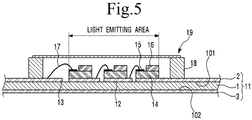
- the luminescence device may include a direct copper bonding (DCB) substrate 11, an LED chip 14, a phosphor 16, a bonding wire 17, a dam 18 and an encapsulation layer "S".
- DCB direct copper bonding
- the DCB substrate 11 may include a substrate body 1, a first copper layer 2 and a second copper layer 3.
- the substrate body 1 may be formed of at least any one of a ceramic material, a polymer material, a resin material, a silicon material and the like or by any combination of them and may have a front side 101 and a rear side 102 facing the front side 101.
- the front side 101 and the rear side 102 form the outer surface of the substrate body 1 respectively. If an outer surface of the substrate body 1 is the front side 101, the other outer surface facing the front side 101 may be the rear side 102.
- any material capable of functioning as an insulation layer and a body of the DCB substrate 11 can be used as the material of the substrate body 1.
- any material capable of functioning as an insulation layer and a body of the DCB substrate 11 can be used as the material of the substrate body 1.
- Al 2 O 3 , ALN, BeO and the like may be used as the material of the substrate body 1.
- the first copper layer 2 may be disposed on the front side of the substrate body 1.
- the second copper layer 3 may be disposed on the rear side of the substrate body 1.
- An electrode pattern may be formed on the first copper layer 2 by mask-etching a certain circuit pattern. Therefore, the first copper layer 2 may include a plurality of the electrode patterns.
- the plurality of the electrode patterns may be a first electrode pattern 12 and a second electrode pattern 13.
- the substrate body 1 may have a thickness of 0.2 to 0.32 mm.
- the first copper layer 2 and the second copper layer 3 may have a thickness of 0.15 to 0.25 mm respectively.
- the electrode patterns may be formed to electrically isolated from each other in consideration of heat radiation of the LED chip 14 or junction of the LED chip 14. The electrode patterns may be separated from each other by a distance within a range of 0.25 to 0.4 mm.
- a driving circuit (not shown) for driving the LED chip 14 may be mounted.
- the driving circuit (not shown) may function to drive the LED chip 14 so as to perform functions according to the purpose and use of the luminescence device.
- the DCB substrate 11 is a thermally conductive substrate.
- the DCB substrate 11 may radiate to the outside the heat generated from the LED chip 14.
- the DCB substrate 11 may include the first and the second copper layers 2 and 3.
- first and the second copper layers 2 and 3 are shown in the embodiment, in examples falling outside the scope of the invention as claimed it is also allowed that the first and the second copper layers 2 and 3 are formed of another metal layer.
- the first and the second copper layers 2 and 3 may be formed of a metal layer formed of at least any one selected from the group consisting of Ag, Au, Ni, Al, Cr, Ru, Re, Pb, Sn, In, Zn, Pt, Mo, Ti, Ta, W, etc., or may be formed of an alloy layer formed of the above-described metallic materials
- the LED chip 14 is a kind of light emitting means to emit light.
- the LED chip 14 may be one of a colored LED chip and an UV LED chip.
- the colored LED chip may be formed in the form of a package obtained by combining at least one or more of a blue LED chip, a red LED chip, a green LED chip, a yellow green LED chip and a white LED chip.
- At least one LED chip 14 is mounted in a certain area of the DCB substrate 11, so that the area in which the LED chips 14 are mounted is a light emitting area. More specifically, the LED chip 14 may be mounted in a certain area on the first electrode pattern 12 of the DCB substrate 11.
- Fig. 2 is a cross sectional view showing an enlarged part denoted by 'A' of Fig. 1 .
- the structure of the part denoted by "A” will be described with reference to Fig. 2 .
- the LED chip 14 may be mounted such that a metal film 35 formed on the first electrode pattern 12 and an adhesive "A" applied on the metal film 35 are interposed between the first copper layer 2 and the LED chip 14.
- the metal film 35 may be made of Ag, Au and the like, and the adhesive "A” may be made of AuSn and the like.
- the materials of the metal film 35 and the adhesive "A” are not limited to this.
- the metal film 35 may be formed only on the portion on which the LED chip 14 is mounted. Due to the metal film 35, a mounting force between the first electrode pattern 12 and the LED chip 14 may be improved.
- a plurality of voids 31 may be formed in the surface of the first copper layer 2 including the first electrode pattern 12 by grain boundary of the first copper layer 2. Due to the void 31, the mounting force between the first electrode pattern 12 and the LED chip 14 may be reduced. However, since the void 31 is filled with the metal film 35 by forming the metal film 35 on the first copper layer 2, the mounting force between the first electrode pattern 12 and the LED chip 14 may be enhanced by the metal film 35.
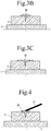
- Figs. 3a to 3c are cross sectional views for describing a method for forming the metal film of the DCB substrate of Fig. 1 .
- a metal paste 33 may be applied on the surface of the first copper layer 2 in which the void 31 has been positioned.
- the metal paste 33 may be applied on the portion on which the LED chip 14 is mounted and on the portion to which the bonding wire 17 is bonded.
- the metal paste 31 is sequentially dried, fired and flattened. Then, the metal film 35 which fills the void 31 may be positioned on the surface of the first copper layer 2.
- an anti-corrosion layer (not shown) for preventing copper from being corroded may be further positioned on the surface having no metal film 35 disposed thereon of the first copper layer 2.
- the LED chip 14 may include the electrode pad 15.
- the electrode pad 15 may be disposed in a predetermined area of the top surface of the LED chip14 in a direction in which the second electrode pattern 13 is disposed.
- the bonding wire 17 may be bonded to the second electrode pattern 13 and the electrode pad 15 of the LED chip 14 mounted on the first electrode pattern 12 respectively.
- the second electrode pattern 13 and the electrode pad 15 of the LED chip 14 mounted on the first electrode pattern 12 may be electrically connected to each other through the bonding wire 17.
- the bonding wire 17 may be formed of a material having an excellent electrical conductivity, e.g., Au, Ag and the like.
- Fig. 4 is a cross sectional view showing an enlarged part denoted by 'B' of Fig. 1 .
- the bonding wire 17 may be, as shown in Fig. 4 , bonded to the metal film 35 disposed on the second electrode pattern 13.
- the metal film 35 is disposed only on the portion to which the bonding wire 17 is bonded. Thus, the metal film 35 is able to improve the bonding force between the second electrode pattern 13 and the bonding wire 17. That is, as shown in Fig. 3a , a plurality of voids 31 may be disposed in the surface of the first copper layer 2 including the second electrode pattern 13 by grain boundary of the first copper layer 2. Due to the void 31, the bonding force between the second electrode pattern 13 and the bonding wire 17 may be reduced. However, since the void 31 is filled with the metal film 35, the bonding force between the second electrode pattern 13 and the bonding wire 17 may be enhanced by the metal film 35. Since a method for forming the metal film 35 is the same as the aforementioned method, a detailed description thereof will be omitted.
- the phosphor 16 may be disposed adjacent to the electrode pad 15 on the LED chip 14.
- the phosphor 16 may include at least one kind of the phosphor.
- the phosphor 16 may function to excite light emitted from the LED chip 14.
- the phosphor 16 may include at least one of a silicate based phosphor, a sulfide based phosphor, a YAG based phosphor, a TAG based phosphor and a nitride based phosphor.
- the dam 18 is made of an insulation material.
- the dam 18 may be disposed on the DCB substrate 11 outside the first and the second electrode patterns 12 and 13.
- the dam 18 may be formed taller than the LED chip 14.
- the dam 18 may have a variety of shapes.
- the dam 18 may have any one of shapes of a hemisphere, a semi-ellipse, a semi-circle, a quadrangle and a quadrangle having an upper chamfered edge.
- Reference light generated from the LED chip 14 may travel upward.
- the reference light may be mixed with secondary excited light which is absorbed by the phosphor injected into the encapsulation layer "S" and is re-emitted. Accordingly, the reference light may be represented by a white color.
- the encapsulation layer "S” since the deviation and uniformity difference of the color are caused depending on the shape of the encapsulation layer "S" into which the phosphor has been injected, the encapsulation layer "S" may be formed flat.
- the luminescence device according to the first embodiment includes the DCB substrate 11 and the LED chip 14 mounted on the DCB substrate 11, the LED chip 14 is directly mounted on the DCB substrate 11 without both the electrode pattern disposed separately from the substrate and the heat sink layer disposed on the electrode pattern, so that the height of the luminescence device can be reduced.
- the metal film 35 is disposed to fill the void 31 which has been positioned in the surface of the first electrode pattern 12, on which the LED chip 14 is mounted, and in the surface of the second electrode pattern 13, to which the bonding wire 17 connected to the electrode pattern 15 is bonded. Accordingly, it is possible to improve the mounting force between the first electrode pattern 12 and the LED chip 14 and to improve the bonding force between the second electrode pattern 13 and the bonding wire 17.
- Fig. 5 is a cross sectional view of a luminescence device according to a second embodiment.
- the luminescence device may include the DCB substrate 11, the LED chip 14, the phosphor 16, the bonding wire 17, the dam 18 and a reflection preventing glass 19.
- the configuration of the substrate 11, the LED chip 14, the bonding wire 17 and the dam 18 is the same as that of the foregoing first embodiment, a detailed description thereof will be omitted.
- the metal film 35 formed to fill the void 31 which has been disposed in the surface of the first electrode pattern 12, on which the LED chip 14 is mounted, and in the surface of the second electrode pattern 13, to which the bonding wire 17 connected to the electrode pattern 15 is bonded is the same as that of the foregoing first embodiment. Therefore, a detailed description thereof will be omitted as well.
- the phosphor 16 may be disposed adjacent to the electrode pad 15 on the LED chip 14.
- the phosphor 16 may include at least one kind of the phosphor.
- the phosphor 16 may function to excite light emitted from the LED chip 14.
- the phosphor 16 may include at least one of a silicate based phosphor, a sulfide based phosphor, a YAG based phosphor, a TAG based phosphor and a nitride based phosphor.
- the phosphor 16 may include a green phosphor and a red phosphor. Further, when the LED chip 14 emits blue light, the phosphor 16 may include a green phosphor, a yellow phosphor and a red phosphor.
- the reflection preventing glass 19 may be disposed above the first and the second electrode patterns 12 and 13 and on the dam 18 in parallel with the DCB substrate 11.
- the reflection preventing glass 19 may be spaced from the phosphor 16.
- a film may be used as the reflection preventing glass 19.
- the reflectance of the reflection preventing glass 19 is less than that of a resin. Therefore, the reflection preventing glass 19 is able to reduce a light emitting area by suppressing light diffusion.
- the light emitting area for 30 LED chips 14 may be 140 mm 2 .
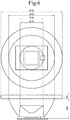
- Fig. 6 is a schematic view showing a luminescence device in which an LED chip and a lens of Fig. 5 are coupled to each other.
- the luminescence device according to the second embodiment includes the DCB substrate 11 and the LED chip 14 mounted on the DCB substrate 11, the luminescence device may not include the electrode pattern disposed separately from the substrate and the heat sink layer disposed on the electrode pattern. Accordingly, the LED chip 14 is directly mounted on the DCB substrate 11, so that the height of the luminescence device can be reduced.
- the luminescence device includes the phosphor 16 disposed on the LED chip 14, thereby reducing the area of the luminescence device and improving the luminance of the luminescence device.
- the luminescence device includes the reflection preventing glass 19, thereby suppressing the light diffusion and reducing the light emitting area.
- the luminescence device includes, as shown in Fig. 6 , a lens. Inner and outer diameters of the inner surface of the lens are 23.24 mm and 23.85 mm respectively.
- Table 1 Edison embodiment light emitting area of COB (mm) 23 11.8 height (mm) 44.2 22 outer diameter (mm) 87 60 effective diameter (mm) 70 44 field angle (°) 60 (medium angle) 58 (medium angle) beam angle (°) 33 geometrical efficiency 96.4
- the luminescence device uses Au as the metal layer of the substrate, to thereby restraining the emitted light from being discolored.
- the luminescence device is hereby able to inhibit the degradation of luminous flux. That is, since the luminescence device includes the phosphor 16 disposed on the LED chip 14 and the reflection preventing glass 19 disposed spaced from the phosphor 16, little light reaches the first and the second electrode patterns 12 and 13, and thus, Au with a low reflectance can be used as the metal layer of the substrate.
- the metal film 35 is disposed to fill the void 31 which has been positioned in the surface of the first electrode pattern 12, on which the LED chip 14 is mounted, and in the surface of the second electrode pattern 13, to which the bonding wire 17 connected to the electrode pattern 15 is bonded. Accordingly, it is possible to improve the mounting force between the first electrode pattern 12 and the LED chip 14 and to improve the bonding force between the second electrode pattern 13 and the bonding wire 17.
- any reference in this specification to "one embodiment,” “an embodiment,” “example embodiment,” etc. means that a particular feature, structure, or characteristic described in connection with the embodiment is included in at least one embodiment of the invention.
- the appearances of such phrases in various places in the specification are not necessarily all referring to the same embodiment.
Landscapes
- Engineering & Computer Science (AREA)
- Microelectronics & Electronic Packaging (AREA)
- Computer Hardware Design (AREA)
- Power Engineering (AREA)
- Manufacturing & Machinery (AREA)
- Physics & Mathematics (AREA)
- Geometry (AREA)
- Condensed Matter Physics & Semiconductors (AREA)
- General Physics & Mathematics (AREA)
- Led Device Packages (AREA)
- Fastening Of Light Sources Or Lamp Holders (AREA)
- Planar Illumination Modules (AREA)
Claims (14)
- Un dispositif de luminescence comprenant :un substrat (11) comprenant une première électrode (12) et une deuxième électrode (13) ;une puce à DEL (14) disposée sur la première électrode (12) ;un fil de liaison (17) reliant électriquement la puce à DEL (14) et la deuxième électrode (13) ; etun barrage (18) disposé sur le substrat (11),le barrage (18) étant disposé de façon espacée de la puce à DEL (14),le substrat (11) comprenant un substrat de liaison (11) direct en cuivre (DCB) comprenant une première couche de cuivre (2), une deuxième couche de cuivre (3) et un corps de substrat,la première électrode (12) et la deuxième électrode (13) comprenant respectivement un film métallique (35),caractérisé en ce quele film métallique (35) remplit un vide de ses surfaces, eten ce que le film métallique (35) est disposé en appliquant une pâte métallique sur la surface dans laquelle le vide a été positionné, puis en séchant, en cuisant et en aplatissant la pâte métallique.
- Le dispositif de luminescence selon la revendication 1, dans lequel le film métallique (35) comprend au moins l'un parmi Au et Ag.
- Le dispositif de luminescence selon l'une quelconque des revendications 1 à 2, dans lequel la puce à DEL (14) est disposée sur le film métallique (35) de la première électrode (12), et dans lequel la puce à DEL (14) et le film de métal (35) de la première électrode (12) sont liés l'un à l'autre par un adhésif (A).
- Le dispositif de luminescence selon la revendication 4, dans lequel l'adhésif (A) comprend de l'AuSn.
- Le dispositif de luminescence selon l'une quelconque des revendications 1 à 4, dans lequel le corps de substrat est disposé entre la première couche de cuivre (2) et la deuxième couche de cuivre (3).
- Le dispositif de luminescence selon l'une quelconque des revendications 1 à 5, comprenant en outre un phosphore qui excite la lumière émise par la puce à DEL (14), le phosphore étant disposé sur la puce à DEL (14).
- Le dispositif de luminescence selon la revendication 6, dans lequel le phosphore comprend au moins l'un des composés choisis parmi : un phosphore à base de silicate, un phosphore à base de sulfure, un phosphore à base de YAG, un phosphore à base de TAG et un phosphore à base de nitrure.
- Le dispositif de luminescence selon l'une quelconque des revendications 1 à 7, dans lequel le barrage (18) est un matériau d'isolation.
- Le dispositif de luminescence selon l'une quelconque des revendications 1 à 8, dans lequel la hauteur du barrage (18) est supérieure à la hauteur de la puce à DEL (14).
- Le dispositif de luminescence selon l'une quelconque des revendications 1 à 9, comprenant en outre une couche d'encapsulation (S) disposée sur la première et la deuxième électrode (12, 13).
- Le dispositif de luminescence selon la revendication 10, dans lequel la couche d'encapsulation (S) est une résine protectrice transmettant la lumière.
- Le dispositif de luminescence selon l'une quelconque des revendications 1 à 11, comprenant en outre un verre (19) empêchant la réflexion, disposé au-dessus de la première et de la deuxième électrode (12, 13) et qui est parallèle au substrat (11).
- Le dispositif de luminescence selon l'une quelconque des revendications 1 à 12, comprenant en outre une couche anti-corrosion disposée sur une surface de la première couche de cuivre (2).
- Le dispositif de luminescence selon l'une quelconque des revendications 1 à 13, dans lequel le barrage (18) a l'une quelconque des formes d'un hémisphère, d'une demi-ellipse, d'un demi-cercle, d'un quadrilatère et d'un quadrilatère ayant un bord chanfreiné supérieur.
Applications Claiming Priority (1)
| Application Number | Priority Date | Filing Date | Title |
|---|---|---|---|
| KR1020120108580A KR101901890B1 (ko) | 2012-09-28 | 2012-09-28 | 발광 장치 |
Publications (3)
| Publication Number | Publication Date |
|---|---|
| EP2713411A2 EP2713411A2 (fr) | 2014-04-02 |
| EP2713411A3 EP2713411A3 (fr) | 2016-03-16 |
| EP2713411B1 true EP2713411B1 (fr) | 2018-10-31 |
Family
ID=49231347
Family Applications (1)
| Application Number | Title | Priority Date | Filing Date |
|---|---|---|---|
| EP13185895.3A Active EP2713411B1 (fr) | 2012-09-28 | 2013-09-25 | Dispositif de luminescence |
Country Status (5)
| Country | Link |
|---|---|
| US (1) | US9093281B2 (fr) |
| EP (1) | EP2713411B1 (fr) |
| JP (1) | JP6426332B2 (fr) |
| KR (1) | KR101901890B1 (fr) |
| CN (1) | CN103715190B (fr) |
Families Citing this family (3)
| Publication number | Priority date | Publication date | Assignee | Title |
|---|---|---|---|---|
| KR20140047750A (ko) * | 2012-10-09 | 2014-04-23 | 엘지이노텍 주식회사 | 발광 장치 |
| JP2017050445A (ja) * | 2015-09-03 | 2017-03-09 | パナソニックIpマネジメント株式会社 | 発光装置、及び照明装置 |
| JPWO2017209143A1 (ja) * | 2016-05-31 | 2019-03-28 | シチズン電子株式会社 | 発光装置およびその製造方法 |
Family Cites Families (23)
| Publication number | Priority date | Publication date | Assignee | Title |
|---|---|---|---|---|
| JPS5066154U (fr) * | 1973-10-19 | 1975-06-14 | ||
| JPS5936980A (ja) * | 1983-07-04 | 1984-02-29 | Hitachi Ltd | セラミック配線基板とその製造方法 |
| JPH01272183A (ja) * | 1988-04-25 | 1989-10-31 | Toshiba Corp | セラミックス回路基板 |
| US6583444B2 (en) * | 1997-02-18 | 2003-06-24 | Tessera, Inc. | Semiconductor packages having light-sensitive chips |
| JP2002313835A (ja) * | 2001-04-09 | 2002-10-25 | Oki Electric Ind Co Ltd | ボンディングパッド、半導体装置及びワイヤボンディング方法 |
| KR100407051B1 (ko) * | 2001-11-16 | 2003-11-28 | 삼성전자주식회사 | 홈네트워크 시스템 |
| KR20040073974A (ko) * | 2003-02-14 | 2004-08-21 | 롬 앤드 하스 일렉트로닉 머트어리얼즈, 엘.엘.씨. | 전기도금 조성물 |
| US8125137B2 (en) * | 2005-01-10 | 2012-02-28 | Cree, Inc. | Multi-chip light emitting device lamps for providing high-CRI warm white light and light fixtures including the same |
| JP2008277689A (ja) * | 2007-05-07 | 2008-11-13 | C I Kasei Co Ltd | 発光装置および発光装置の作製方法 |
| JP2009033088A (ja) | 2007-06-29 | 2009-02-12 | Sharp Corp | 半導体発光装置、その製造方法およびそれを用いたled照明装置 |
| JP5171288B2 (ja) * | 2008-01-28 | 2013-03-27 | シャープ株式会社 | 固体撮像装置、固体撮像装置の実装方法、固体撮像装置の製造方法、および電子情報機器 |
| WO2010074184A1 (fr) * | 2008-12-26 | 2010-07-01 | 古河電気工業株式会社 | Grille de connexion pour dispositif à semi-conducteurs optique, son procédé de fabrication et dispositif à semi-conducteurs optique |
| US8138509B2 (en) * | 2009-02-27 | 2012-03-20 | Visera Technologies Company, Limited | Light emitting device having luminescent layer with opening to exposed bond pad on light emitting die for wire bonding pad to substrate |
| JP5286122B2 (ja) | 2009-03-23 | 2013-09-11 | スタンレー電気株式会社 | 半導体発光装置および半導体発光装置の製造方法 |
| JP2011071407A (ja) * | 2009-09-28 | 2011-04-07 | Sharp Corp | 発光素子および照明装置 |
| JP2011097038A (ja) | 2009-10-02 | 2011-05-12 | Ibiden Co Ltd | セラミック配線基板およびその製造方法 |
| CN102074558B (zh) * | 2009-10-21 | 2013-06-19 | 东芝照明技术株式会社 | 发光装置以及照明器具 |
| JP5375552B2 (ja) * | 2009-11-24 | 2013-12-25 | 東芝ライテック株式会社 | 発光装置及びこれを備えた照明器具 |
| EP2315284A3 (fr) * | 2009-10-21 | 2013-03-27 | Toshiba Lighting & Technology Corporation | Appareil électroluminescent et luminaire |
| CN102097425A (zh) * | 2009-12-09 | 2011-06-15 | 三星Led株式会社 | 发光二极管、制造磷光体层的方法和发光装置 |
| JP5846408B2 (ja) * | 2010-05-26 | 2016-01-20 | 東芝ライテック株式会社 | 発光装置および照明装置 |
| JP4887529B1 (ja) * | 2011-04-12 | 2012-02-29 | 国立大学法人九州工業大学 | Ledパッケージの製造方法 |
| US8704262B2 (en) * | 2011-08-11 | 2014-04-22 | Goldeneye, Inc. | Solid state light sources with common luminescent and heat dissipating surfaces |
-
2012
- 2012-09-28 KR KR1020120108580A patent/KR101901890B1/ko active IP Right Grant
-
2013
- 2013-08-30 US US14/014,777 patent/US9093281B2/en active Active
- 2013-09-05 JP JP2013183677A patent/JP6426332B2/ja active Active
- 2013-09-25 EP EP13185895.3A patent/EP2713411B1/fr active Active
- 2013-09-27 CN CN201310451485.1A patent/CN103715190B/zh active Active
Non-Patent Citations (1)
| Title |
|---|
| None * |
Also Published As
| Publication number | Publication date |
|---|---|
| EP2713411A2 (fr) | 2014-04-02 |
| US20140091345A1 (en) | 2014-04-03 |
| KR20140042187A (ko) | 2014-04-07 |
| KR101901890B1 (ko) | 2018-09-28 |
| CN103715190A (zh) | 2014-04-09 |
| US9093281B2 (en) | 2015-07-28 |
| JP6426332B2 (ja) | 2018-11-21 |
| JP2014072520A (ja) | 2014-04-21 |
| EP2713411A3 (fr) | 2016-03-16 |
| CN103715190B (zh) | 2018-03-09 |
Similar Documents
| Publication | Publication Date | Title |
|---|---|---|
| EP2811517B1 (fr) | Dispositif électroluminescent | |
| JP5768435B2 (ja) | 発光装置 | |
| JP4881358B2 (ja) | 発光装置 | |
| TWI487148B (zh) | 發光裝置封裝件 | |
| US9420642B2 (en) | Light emitting apparatus and lighting apparatus | |
| JP2008071954A (ja) | 光源装置 | |
| JP6583764B2 (ja) | 発光装置、及び照明装置 | |
| WO2011129203A1 (fr) | Dispositif émetteur de lumière | |
| JP5598323B2 (ja) | 発光装置および発光装置の製造方法 | |
| EP2720266B1 (fr) | Dispositif de luminescence | |
| JP2007258620A (ja) | 発光装置 | |
| JP2006147865A (ja) | 発光素子実装用基板とその製造方法、発光素子モジュールとその製造方法、表示装置、照明装置及び交通信号機 | |
| JP2008218998A (ja) | 発光装置 | |
| JP2008140934A (ja) | 発光ダイオード装置及び照明装置 | |
| JP2007288138A (ja) | 発光装置 | |
| EP2713411B1 (fr) | Dispositif de luminescence | |
| JP2012216726A (ja) | 半導体発光装置 | |
| KR20110089068A (ko) | 화합물반도체소자 수납용 패키지 및 그 제조방법 | |
| JP2008244468A (ja) | 発光装置 | |
| KR101173398B1 (ko) | 발광다이오드 수납용 패키지 및 그 제조방법 | |
| JP2008244469A (ja) | 発光装置 | |
| US9887179B2 (en) | Light emitting diode device and light emitting device using the same | |
| JP2008021795A (ja) | 光源装置 | |
| KR101456921B1 (ko) | 세라믹 pcb를 이용한 led 광원모듈 및 그 제조방법 | |
| JP7494017B2 (ja) | 発光モジュール及び発光モジュールの製造方法 |
Legal Events
| Date | Code | Title | Description |
|---|---|---|---|
| PUAI | Public reference made under article 153(3) epc to a published international application that has entered the european phase |
Free format text: ORIGINAL CODE: 0009012 |
|
| AK | Designated contracting states |
Kind code of ref document: A2 Designated state(s): AL AT BE BG CH CY CZ DE DK EE ES FI FR GB GR HR HU IE IS IT LI LT LU LV MC MK MT NL NO PL PT RO RS SE SI SK SM TR |
|
| AX | Request for extension of the european patent |
Extension state: BA ME |
|
| PUAL | Search report despatched |
Free format text: ORIGINAL CODE: 0009013 |
|
| AK | Designated contracting states |
Kind code of ref document: A3 Designated state(s): AL AT BE BG CH CY CZ DE DK EE ES FI FR GB GR HR HU IE IS IT LI LT LU LV MC MK MT NL NO PL PT RO RS SE SI SK SM TR |
|
| AX | Request for extension of the european patent |
Extension state: BA ME |
|
| RIC1 | Information provided on ipc code assigned before grant |
Ipc: H01L 23/373 20060101ALN20160211BHEP Ipc: H01L 33/50 20100101ALN20160211BHEP Ipc: H01L 33/62 20100101AFI20160211BHEP Ipc: H01L 33/64 20100101ALN20160211BHEP |
|
| 17P | Request for examination filed |
Effective date: 20160914 |
|
| RBV | Designated contracting states (corrected) |
Designated state(s): AL AT BE BG CH CY CZ DE DK EE ES FI FR GB GR HR HU IE IS IT LI LT LU LV MC MK MT NL NO PL PT RO RS SE SI SK SM TR |
|
| RAP1 | Party data changed (applicant data changed or rights of an application transferred) |
Owner name: LG INNOTEK CO., LTD. |
|
| GRAP | Despatch of communication of intention to grant a patent |
Free format text: ORIGINAL CODE: EPIDOSNIGR1 |
|
| STAA | Information on the status of an ep patent application or granted ep patent |
Free format text: STATUS: GRANT OF PATENT IS INTENDED |
|
| INTG | Intention to grant announced |
Effective date: 20180329 |
|
| RIC1 | Information provided on ipc code assigned before grant |
Ipc: H01L 33/50 20100101ALN20180316BHEP Ipc: H01L 33/64 20100101ALN20180316BHEP Ipc: H01L 33/62 20100101AFI20180316BHEP Ipc: H01L 23/373 20060101ALN20180316BHEP |
|
| GRAS | Grant fee paid |
Free format text: ORIGINAL CODE: EPIDOSNIGR3 |
|
| GRAA | (expected) grant |
Free format text: ORIGINAL CODE: 0009210 |
|
| STAA | Information on the status of an ep patent application or granted ep patent |
Free format text: STATUS: THE PATENT HAS BEEN GRANTED |
|
| AK | Designated contracting states |
Kind code of ref document: B1 Designated state(s): AL AT BE BG CH CY CZ DE DK EE ES FI FR GB GR HR HU IE IS IT LI LT LU LV MC MK MT NL NO PL PT RO RS SE SI SK SM TR |
|
| REG | Reference to a national code |
Ref country code: CH Ref legal event code: EP Ref country code: GB Ref legal event code: FG4D |
|
| REG | Reference to a national code |
Ref country code: AT Ref legal event code: REF Ref document number: 1060443 Country of ref document: AT Kind code of ref document: T Effective date: 20181115 |
|
| REG | Reference to a national code |
Ref country code: DE Ref legal event code: R096 Ref document number: 602013045855 Country of ref document: DE |
|
| REG | Reference to a national code |
Ref country code: IE Ref legal event code: FG4D |
|
| REG | Reference to a national code |
Ref country code: NL Ref legal event code: MP Effective date: 20181031 |
|
| REG | Reference to a national code |
Ref country code: LT Ref legal event code: MG4D |
|
| REG | Reference to a national code |
Ref country code: AT Ref legal event code: MK05 Ref document number: 1060443 Country of ref document: AT Kind code of ref document: T Effective date: 20181031 |
|
| PG25 | Lapsed in a contracting state [announced via postgrant information from national office to epo] |
Ref country code: BG Free format text: LAPSE BECAUSE OF FAILURE TO SUBMIT A TRANSLATION OF THE DESCRIPTION OR TO PAY THE FEE WITHIN THE PRESCRIBED TIME-LIMIT Effective date: 20190131 Ref country code: NO Free format text: LAPSE BECAUSE OF FAILURE TO SUBMIT A TRANSLATION OF THE DESCRIPTION OR TO PAY THE FEE WITHIN THE PRESCRIBED TIME-LIMIT Effective date: 20190131 Ref country code: LT Free format text: LAPSE BECAUSE OF FAILURE TO SUBMIT A TRANSLATION OF THE DESCRIPTION OR TO PAY THE FEE WITHIN THE PRESCRIBED TIME-LIMIT Effective date: 20181031 Ref country code: ES Free format text: LAPSE BECAUSE OF FAILURE TO SUBMIT A TRANSLATION OF THE DESCRIPTION OR TO PAY THE FEE WITHIN THE PRESCRIBED TIME-LIMIT Effective date: 20181031 Ref country code: LV Free format text: LAPSE BECAUSE OF FAILURE TO SUBMIT A TRANSLATION OF THE DESCRIPTION OR TO PAY THE FEE WITHIN THE PRESCRIBED TIME-LIMIT Effective date: 20181031 Ref country code: HR Free format text: LAPSE BECAUSE OF FAILURE TO SUBMIT A TRANSLATION OF THE DESCRIPTION OR TO PAY THE FEE WITHIN THE PRESCRIBED TIME-LIMIT Effective date: 20181031 Ref country code: AT Free format text: LAPSE BECAUSE OF FAILURE TO SUBMIT A TRANSLATION OF THE DESCRIPTION OR TO PAY THE FEE WITHIN THE PRESCRIBED TIME-LIMIT Effective date: 20181031 Ref country code: PL Free format text: LAPSE BECAUSE OF FAILURE TO SUBMIT A TRANSLATION OF THE DESCRIPTION OR TO PAY THE FEE WITHIN THE PRESCRIBED TIME-LIMIT Effective date: 20181031 Ref country code: IS Free format text: LAPSE BECAUSE OF FAILURE TO SUBMIT A TRANSLATION OF THE DESCRIPTION OR TO PAY THE FEE WITHIN THE PRESCRIBED TIME-LIMIT Effective date: 20190228 Ref country code: FI Free format text: LAPSE BECAUSE OF FAILURE TO SUBMIT A TRANSLATION OF THE DESCRIPTION OR TO PAY THE FEE WITHIN THE PRESCRIBED TIME-LIMIT Effective date: 20181031 |
|
| PG25 | Lapsed in a contracting state [announced via postgrant information from national office to epo] |
Ref country code: SE Free format text: LAPSE BECAUSE OF FAILURE TO SUBMIT A TRANSLATION OF THE DESCRIPTION OR TO PAY THE FEE WITHIN THE PRESCRIBED TIME-LIMIT Effective date: 20181031 Ref country code: AL Free format text: LAPSE BECAUSE OF FAILURE TO SUBMIT A TRANSLATION OF THE DESCRIPTION OR TO PAY THE FEE WITHIN THE PRESCRIBED TIME-LIMIT Effective date: 20181031 Ref country code: GR Free format text: LAPSE BECAUSE OF FAILURE TO SUBMIT A TRANSLATION OF THE DESCRIPTION OR TO PAY THE FEE WITHIN THE PRESCRIBED TIME-LIMIT Effective date: 20190201 Ref country code: PT Free format text: LAPSE BECAUSE OF FAILURE TO SUBMIT A TRANSLATION OF THE DESCRIPTION OR TO PAY THE FEE WITHIN THE PRESCRIBED TIME-LIMIT Effective date: 20190301 Ref country code: RS Free format text: LAPSE BECAUSE OF FAILURE TO SUBMIT A TRANSLATION OF THE DESCRIPTION OR TO PAY THE FEE WITHIN THE PRESCRIBED TIME-LIMIT Effective date: 20181031 Ref country code: NL Free format text: LAPSE BECAUSE OF FAILURE TO SUBMIT A TRANSLATION OF THE DESCRIPTION OR TO PAY THE FEE WITHIN THE PRESCRIBED TIME-LIMIT Effective date: 20181031 |
|
| PG25 | Lapsed in a contracting state [announced via postgrant information from national office to epo] |
Ref country code: IT Free format text: LAPSE BECAUSE OF FAILURE TO SUBMIT A TRANSLATION OF THE DESCRIPTION OR TO PAY THE FEE WITHIN THE PRESCRIBED TIME-LIMIT Effective date: 20181031 Ref country code: DK Free format text: LAPSE BECAUSE OF FAILURE TO SUBMIT A TRANSLATION OF THE DESCRIPTION OR TO PAY THE FEE WITHIN THE PRESCRIBED TIME-LIMIT Effective date: 20181031 Ref country code: CZ Free format text: LAPSE BECAUSE OF FAILURE TO SUBMIT A TRANSLATION OF THE DESCRIPTION OR TO PAY THE FEE WITHIN THE PRESCRIBED TIME-LIMIT Effective date: 20181031 |
|
| REG | Reference to a national code |
Ref country code: DE Ref legal event code: R097 Ref document number: 602013045855 Country of ref document: DE |
|
| PG25 | Lapsed in a contracting state [announced via postgrant information from national office to epo] |
Ref country code: SM Free format text: LAPSE BECAUSE OF FAILURE TO SUBMIT A TRANSLATION OF THE DESCRIPTION OR TO PAY THE FEE WITHIN THE PRESCRIBED TIME-LIMIT Effective date: 20181031 Ref country code: EE Free format text: LAPSE BECAUSE OF FAILURE TO SUBMIT A TRANSLATION OF THE DESCRIPTION OR TO PAY THE FEE WITHIN THE PRESCRIBED TIME-LIMIT Effective date: 20181031 Ref country code: RO Free format text: LAPSE BECAUSE OF FAILURE TO SUBMIT A TRANSLATION OF THE DESCRIPTION OR TO PAY THE FEE WITHIN THE PRESCRIBED TIME-LIMIT Effective date: 20181031 Ref country code: SK Free format text: LAPSE BECAUSE OF FAILURE TO SUBMIT A TRANSLATION OF THE DESCRIPTION OR TO PAY THE FEE WITHIN THE PRESCRIBED TIME-LIMIT Effective date: 20181031 |
|
| PLBE | No opposition filed within time limit |
Free format text: ORIGINAL CODE: 0009261 |
|
| STAA | Information on the status of an ep patent application or granted ep patent |
Free format text: STATUS: NO OPPOSITION FILED WITHIN TIME LIMIT |
|
| 26N | No opposition filed |
Effective date: 20190801 |
|
| PG25 | Lapsed in a contracting state [announced via postgrant information from national office to epo] |
Ref country code: SI Free format text: LAPSE BECAUSE OF FAILURE TO SUBMIT A TRANSLATION OF THE DESCRIPTION OR TO PAY THE FEE WITHIN THE PRESCRIBED TIME-LIMIT Effective date: 20181031 |
|
| PG25 | Lapsed in a contracting state [announced via postgrant information from national office to epo] |
Ref country code: TR Free format text: LAPSE BECAUSE OF FAILURE TO SUBMIT A TRANSLATION OF THE DESCRIPTION OR TO PAY THE FEE WITHIN THE PRESCRIBED TIME-LIMIT Effective date: 20181031 |
|
| PG25 | Lapsed in a contracting state [announced via postgrant information from national office to epo] |
Ref country code: MC Free format text: LAPSE BECAUSE OF FAILURE TO SUBMIT A TRANSLATION OF THE DESCRIPTION OR TO PAY THE FEE WITHIN THE PRESCRIBED TIME-LIMIT Effective date: 20181031 |
|
| REG | Reference to a national code |
Ref country code: CH Ref legal event code: PL |
|
| PG25 | Lapsed in a contracting state [announced via postgrant information from national office to epo] |
Ref country code: CH Free format text: LAPSE BECAUSE OF NON-PAYMENT OF DUE FEES Effective date: 20190930 Ref country code: LU Free format text: LAPSE BECAUSE OF NON-PAYMENT OF DUE FEES Effective date: 20190925 Ref country code: LI Free format text: LAPSE BECAUSE OF NON-PAYMENT OF DUE FEES Effective date: 20190930 Ref country code: IE Free format text: LAPSE BECAUSE OF NON-PAYMENT OF DUE FEES Effective date: 20190925 |
|
| REG | Reference to a national code |
Ref country code: BE Ref legal event code: MM Effective date: 20190930 |
|
| PG25 | Lapsed in a contracting state [announced via postgrant information from national office to epo] |
Ref country code: BE Free format text: LAPSE BECAUSE OF NON-PAYMENT OF DUE FEES Effective date: 20190930 |
|
| GBPC | Gb: european patent ceased through non-payment of renewal fee |
Effective date: 20190925 |
|
| PG25 | Lapsed in a contracting state [announced via postgrant information from national office to epo] |
Ref country code: GB Free format text: LAPSE BECAUSE OF NON-PAYMENT OF DUE FEES Effective date: 20190925 |
|
| PG25 | Lapsed in a contracting state [announced via postgrant information from national office to epo] |
Ref country code: CY Free format text: LAPSE BECAUSE OF FAILURE TO SUBMIT A TRANSLATION OF THE DESCRIPTION OR TO PAY THE FEE WITHIN THE PRESCRIBED TIME-LIMIT Effective date: 20181031 |
|
| PG25 | Lapsed in a contracting state [announced via postgrant information from national office to epo] |
Ref country code: HU Free format text: LAPSE BECAUSE OF FAILURE TO SUBMIT A TRANSLATION OF THE DESCRIPTION OR TO PAY THE FEE WITHIN THE PRESCRIBED TIME-LIMIT; INVALID AB INITIO Effective date: 20130925 Ref country code: MT Free format text: LAPSE BECAUSE OF FAILURE TO SUBMIT A TRANSLATION OF THE DESCRIPTION OR TO PAY THE FEE WITHIN THE PRESCRIBED TIME-LIMIT Effective date: 20181031 Ref country code: FR Free format text: LAPSE BECAUSE OF NON-PAYMENT OF DUE FEES Effective date: 20190930 |
|
| REG | Reference to a national code |
Ref country code: DE Ref legal event code: R081 Ref document number: 602013045855 Country of ref document: DE Owner name: SUZHOU LEKIN SEMICONDUCTOR CO. LTD., TAICANG, CN Free format text: FORMER OWNER: LG INNOTEK CO., LTD., SEOUL, KR |
|
| PG25 | Lapsed in a contracting state [announced via postgrant information from national office to epo] |
Ref country code: MK Free format text: LAPSE BECAUSE OF FAILURE TO SUBMIT A TRANSLATION OF THE DESCRIPTION OR TO PAY THE FEE WITHIN THE PRESCRIBED TIME-LIMIT Effective date: 20181031 |
|
| PGFP | Annual fee paid to national office [announced via postgrant information from national office to epo] |
Ref country code: DE Payment date: 20230808 Year of fee payment: 11 |