従来技術で、DCB基板にこれとは別部品であるベースを接合して、このベース用いてヒートシンク等の被取付け部材にDCB基板を取付ける構成は、部品点数が多くコスト高であるという問題がある。又、第2金属層を接続材料例えば半田でヒートシンク等に取付ける構成では、半田の溶融温度が、鉛フリータイプの場合でも230℃前後で、LEDチップを第1金属層に実装するのに使用する接着剤等の耐熱温度に比べて低いため、高い温度環境での使用、又は点灯消灯に伴う温度変化によって、半田にクラック等の劣化が発生するおそれがある。そのため、従来技術の発光装置において、半田を使用していると、半田を使用していない場合に比べて、半田の劣化を考慮してDCB基板の温度が高くならないように投入電力を抑制しなくてはならず、これにより、LEDチップに供給する電力を増加させて明るさを増やす上では不利である。
こうした事情から、発光装置とは別部品であるベースを用いることなく、DCB基板をヒートシンク等にねじ止めできるようにすることが望まれているが、こうした要請は前記従来技術では満たすことができない。
ところで、DCB基板のセラミックス製絶縁コアにねじ孔を形成すれば、この孔にねじを通してDCB基板をヒートシンク等に取付けることができるが、この取付け構造は以下の点で好ましくない。
第1に、DCB基板をヒートシンク等にねじ止めする際、ねじの締め付けトルクによって、DCB基板のセラミックス製絶縁コアが破損するおそれがある。
第2に、DCB基板がねじ止めされるヒートシンク等の被取付け部材の熱膨張の方が、DCB基板のセラミックス製絶縁コアの熱膨張より大きい。このため、温度上昇により、セラミックス製絶縁コアが、被取付け部材の熱膨張に伴って、この部材と反対側に凸となるように押されて変形することがある。それに伴い、ねじ止め部に負荷が掛かってセラミックス製絶縁コアが破損するおそれがある。
第3に、セラミックス製絶縁コアの裏面に接合されている銅製等の第2金属層の熱膨張の方が、セラミックス製絶縁コアの熱膨張より大きいので、温度上昇に伴う熱膨張差により、セラミックス製絶縁コアが被取付け部材から離れる方向に凸となるように変形することがある。それに伴い、ねじ止め部に負荷が掛かってセラミックス製絶縁コアが破損するおそれがある。
本発明は、以上の事情に基づきなされたもので、部品点数を増加することなく被取付け部材にねじ止めできるとともに、ねじ止め部を原因としてセラミックス製の基材が破損しないようにした発光装置、及びこの装置を備えた照明器具を提供することを目的とする。
上記の課題を解決するために、請求項1に係る発明の発光装置は、実装面及びこの実装面に対して反対側の裏面を有するセラミックス製の基材、前記実装面に直接接合又は蝋着されて所定のパターンで配設された正面金属部材並びに給電部、及び前記裏面に直接接合又は蝋着され、かつ、前記基材の周部より突出された固定部を一体に有しこの固定部にねじ通し部が形成された裏面金属部材を備えた基板と;前記正面金属部材に実装されるとともに前記給電部に電気的に接続された半導体発光素子と;を具備することを特徴としている。
この発明及び以下の発明で、基板には、DCB(Direct Copper Bonding)基板、DBA(Direct Brazing Aluminum)基板、AMC(Active Metal Brazed Copper)基板等を用いることができる。DCB基板は、セラミックス基材に金属部材として銅板を直接接合して形成されたものである。DBA基板は、セラミックス基材に金属部材としてアルミニウム板を蝋着して形成されたものである。AMC基板は、セラミックス基材に金属部材として銅板を蝋着して形成されたものである。
この発明及び以下の発明で、セラミックス基材には、Al2O3、ALN、SiN等の材料を用いることができる。
この発明及び以下の発明で、正面金属部材を所定のパターンで実装面に設けるには、一枚の金属部材を予め金型等で所定のパターンに打ち抜き成形したものを、セラミックス等の基材に接合した後、この金属部材の必要な部分間に設けられていてこの必要部分を支持していたブリッジ部等の不要な部分を切除して実現できる。或いは、一枚の金属部材をセラミックス基材に接合した後、エッチングによって所定のパターンに形成することもできる。
この発明及び以下の発明で、半導体発光素子には、例えばLEDチップや有機EL等を用いることができる。
この発明及び以下の発明で、給電部は、セラミックス等の基材の周部から外側に突出していても、或いは、こうした突出状態に設けられるのではなく、基材の一部に孔又は溝等からなる取付け部を設け、この取付け部から突出された状態に設けられていてもよい。
この発明及び以下の発明で、裏面金属部材の周部全体が、セラミックス等の基材の周部より突出されている場合、この周部に形成されたねじ通し部がある部位を固定部として用いることができる。又、裏面金属部材は、その固定部を除いた領域を基材と略同じ大きさとして、固定部のみが基材の周部から突出されるようにしてもよく、或いは基材の周部に切り欠き状の凹部を設けるとともに、この凹部と基材とを合わせた大きさと略同じ大きさの裏面金属部材を用いて、この部材の前記凹部に露出するように突出された周部の一部を、固定部として用いることもできる。更に、裏面金属部材は、孔や切り欠きがない平板に限らず、例えば、正面金属部材のパターンに応じて、このパターンに粗密がある場合等には、密度が相対的に高い部位に対応して孔や切り欠きを設けることも可能である。
請求項1の発明では、基材の裏面に直接接合又は蝋着により接合された裏面金属部材を基板が備えているので、厚みが厚い板状の裏面金属部材を用いることができる。これにより、裏面金属部材と一体でかつねじ通し部が形成された固定部は、ヒートシンク等の被取付け部材に基板をねじ止めするに足る十分な強度を有する。この固定部は、セラミックス製基材の周りにこの基材の周部から突出されているので、セラミックス製基材にねじを通すことなく、固定部のねじ通し部にねじを通して基板を被取付け部材に固定できる。したがって、部品点数を増加することなく被取付け部材にねじ止めできるとともに、ねじ止め部を原因としてセラミックス製の基材が破損しないようにできる。しかも、固定部は裏面金属部材と一体であるので、固定部として別部品を要することがない。
請求項2の発明は、請求項1に係る発明の発光装置において、前記裏面金属部材の面積が前記正面金属部材の面積より大であるとともに、前記裏面金属部材の厚みが前記正面金属部材の厚みより薄いことを特徴としている。
この発明では、正面金属部材は半導体発光素子の配置に従ったパターンで設けられているので、その面積は裏面金属部材の面積よりも小さい。こうした構成では、基板の製造において、高温条件下で基材に正面及び裏面の金属部材を直接接合又は蝋着した後に常温まで温度降下する場合、正面金属部材よりもボリュームが大きい方の裏面金属部材の熱収縮が大きい。それにより、正面金属部材側が凸となり裏面金属部材側が凹となるように基板が反ることがあり、こうした変形を原因とする様々な悪影響がもたらされる恐れがある。しかし、請求項2の発明では、裏面金属部材の厚みが正面金属部材の厚みより薄いので、前記正面金属部材と裏面金属部材の熱収縮が略同様となるに伴って、基板の前記反りを抑制できる。
請求項3に係る発明の照明器具置は、請求項1又は2に記載の発光装置を光源として具備することを特徴としている。
この発明によれば、部品点数を増加することなく被取付け部材にねじ止めできるとともに、ねじ止め部を原因としてセラミックス製の基材が破損しないようにした発光装置を備えた照明器具を提供できる。
請求項1に係る発明の発光装置によれば、基板の裏面に直接接合又は蝋着により接合された裏面金属部材と一体の固定部のねじ通し部にねじを通して基板を被取付け部材に固定することができるので、部品点数を増加することなく被取付け部材にねじ止めできるとともに、そのねじ止め部でセラミックス製の基材が破損しないようにできる、という効果がある。
請求項2に係る発明の発光装置によれば、請求項1の発明において、更に、製造上等において、正面金属部材と裏面金属部材の面積差に起因する基板の反りを抑制できる、という効果がある。
請求項3に係る発明によれば、部品点数を増加することなく被取付け部材にねじ止めできるとともに、ねじ止め部を原因としてセラミックス製の基材が破損しないようにした発光装置を備えた照明器具を提供できる、という効果がある。
以下、本発明の一実施の形態について、図面を参照して詳細に説明する。
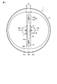
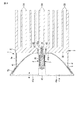
図1〜図4中符号1は照明器具例えば投光器具体的にはスポットライトを示している。スポットライト1は、このライトの光源として用いた一対の発光装置2と、被取付け部材3と、凹面反射鏡4と、鏡支持部材5を具備している。
各発光装置2は、COB(chip on board)型のものであって、図5〜図8に示すように基板11と、複数の半導体発光素子例えばLEDチップ21と、枠部材25と、透光性の封止部材27等を具備している。
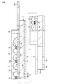
基板11は例えばDCB基板からなる。具体的には、図8等に示すように基材12と、正面金属部材14と、給電部16と、裏面金属部材18を備えている。
基材12は、Al2O3、ALN、SiN等のセラミックス材料の平板で形成されている。図5及び図7に示すように板状の基材12は、その周部例えば四隅の内の二つの隅部に凹部12aを有している。これら一対の凹部12aは、180°隔たって基材12の対角線上に設けられている。これとともに、一対の凹部12aは、基材12の周部を切り欠くように設けられていて、基材12の周面及び厚み方向に夫々開放されている。
図5に示すように基材12の正面をなす一面はLEDチップ21が実装される実装面12bであり、基材12の裏面12cは実装面12bと反対側の他面からなり、これら両面は平行である。
正面金属部材14及び給電部16は基材12に対してその正面側に配置されている。詳しくは、基材12の実装面12bにDCB法により正面金属部材14及び給電部16が直接接合されている。正面金属部材14はLEDチップ21の放熱及びこのチップの光りを反射するために設けられている。
裏面金属部材18は基材12に対してその裏面12c側に配置されている。詳しくは、基材12の裏面12cにDCB法により裏面金属部材18が直接接合されている。正面金属部材14、給電部16、及び裏面金属部材18はいずれも銅板である。
DCB法による直接接合では、銅板の一面に酸化銅被膜を形成し、この酸化銅被膜をセラミックス製の基材12に向けて基材12に前記銅板を配置し、加熱炉において銅板の溶融温度より低く酸化銅被膜の溶融温度より高い温度で加熱することにより、銅板とセラミックス製の基材12の接合界面に共晶溶融物を形成して、この共晶溶融物により前記銅板を基材12の実装面12b又は裏面12cに接合する。
実装面12bに直接接合された正面金属部材14は、マトリクス状に分割された複数のパターン部14aからなる。図9に示すように各パターン部14aは複数のLEDチップ21の実装位置に対応して縦横に間隔的に並べられ既述のようにマトリクス状に配設されている。
実装面12bに直接接合された給電部16は、パターン部14aの配列方向(例えば図9において左右方向)にこれらパターン部14aを間に置いて、これらパターン部14aの両側に隣接して配置されている。これら一対の給電部16の一端部が実装面12bに直接接合されていて、パターン部14aの配列方向の端に配置されたパターン部14aに夫々隣接して設けられている。
各給電部16の他端部は、給電端部16aとして用いられ、基材12の周部から基材12外に向けて真っ直ぐに突出されている。給電端部16aはその高さ位置を変えることなく例えば実装面12bと平行に設けられている。しかし、この給電端部16aは、実装面12bから離れる方向に折れ曲がってから、更に実装面12bと平行になるように折れ曲がることによって、基材12の周部から突出されていてもよい。給電部16は基材12の中心に対し点対称に設けられているとともに、その給電端部16aは図5及び図7に示すように基材12の凹部12aに対してずれて配置されている。給電部16には図示しない給電用の絶縁被覆電線が接続される。
なお、図9に示すようにLEDチップ21を一方の配列方向毎に直列に接続したLED直列回路を複数設けたので、LED直列回路毎に給電をする給電部16が既述のように左右に一対形成されている。しかし、全てのLEDチップ21を直列に接続して給電する場合には、直列接続の両端位置のパターン部14aに隣接して給電部16を形成すれば良い。
正面金属部材14及び給電部16の表面には、これら正面金属部材14及び給電部16より遥かに薄い図示しない金属層が積層されている。この金属層は、前記表面に例えば略3μmの厚みでメッキされたニッケルメッキ層等からなる下地メッキ層と、この上に例えば略0.3μmの厚みでメッキされた表層メッキ層とからなり、表層メッキ層は例えば銅又は銀或いは金等のメッキ層からなる。表層メッキ層を銀メッキ層で形成することは、正面金属部材14をなす各パターン部14aでの光反射性能を高く確保できる点で好ましい。
基材12の実装面12bに正面金属部材14及び給電部16を所定のパターンで配設するには、所定厚みを有する一枚の金属材例えば銅板を、打ち抜きプレス機の金型等で所定のパターンに打ち抜き形成したものを実装面12bに直接接合し、メッキ処理を施した後、実装面12bに接合されている銅板からなる金属材の内で、必要な部位同士を接続していたブリッジ部の不要な部分を切除することによって実現できる。或いは、所定の厚みを有しかつ所定の大きさに形成された一枚の銅板からなる金属材を、基材12の実装面12bに直接接合した後、エッチングによって不要な部位を野祖いて所定のパターンに形成し、その後、残った必要部分、つまり、正面金属部材14及び給電部16に対してメッキ処理を施すことで実現可能である。
基材12の裏面12cにDCB法により直接接合された裏面金属部材18は、基板11の反り防止及び放熱等のために設けられていて、好ましくは図6に示すように基材12の裏面12cの略全域を覆っている。この裏面金属部材18は、平板であるとともに、図5〜図7に示すように複数例えば2箇所に固定部18aを一体に有している。
固定部18aは、基材12の周部より突出されていて、この基材12の前記凹部12aに基材12の裏側から臨んでいる。この固定部18aにねじ通し部例えばねじ通孔19が形成されている。ねじ通し部は切り欠き状の凹みで形成することもできる。
板状の金属素材を材料として基材12に接合された正面金属部材14、給電部16、及び裏面金属部材18の厚みは、これらが基材12に直接接合して設けられることにより所望の厚みとすることができ、例えば200μm〜500μmの範囲で選択される。この厚みは金属メッキ層に比較して遥かに厚く、そのために、機械的強度を確保できる。
更に、裏面金属部材18の厚みは、正面金属部材14の給電部16の厚みより薄い。この裏面金属部材18の厚みは、DCB法による基板11の製造での直接接合後に常温まで温度降下する場合、正面金属部材14側が凸となり裏面金属部材18側が凹となるように基板11が反ることを抑制できるように、正面金属部材14のパターンに応じて定められている。
各LEDチップ21には例えば青色発光をするLEDチップが用いられている。これらのLEDチップ21は、図8に示すようにサファイア等からなる素子基板21a上に単色の青色発光をする半導体発光層21bが積層され、この半導体発光層21b上に正負一対の素子電極21cが互いに配置された半導体ベアチップである。
LEDチップ21は、その半導体発光層21bと反対側に位置する素子基板21aの裏面をダイボンド材22で各パターン部14aに夫々固定することによって基材12の実装面12b上に実装されている。ダイボンド材22は、銀ベースト又は樹脂接着剤例えば透明シリコーン樹脂等からなる。
各LEDチップ21の実装は約300℃の温度をかけながら行われる。この場合、正面金属部材14及び給電部16が基材12の実装面12bに占める面積と、裏面金属部材18が基材12の裏面12cに占める面積との差、言い換えれば、これらの面積と厚みを元に換算が可能な基材表裏面での金属材のボリューム差に基づいて、基材12の実装面12b側が凸となり裏面12c側が凹となるように基材12が反ることを、正面金属部材14及び給電部16の厚みより裏面金属部材18の厚みが薄いことにより抑制できる。
なお、LEDチップ21の実装工程で前記反りが過大に発生すると、ダイボンド材22の厚みを適正に管理することが難しくなる。このようになった場合、ダイボンド材22によりLEDチップ21の実装不良を生じる恐れがあるとともに、点灯時のLEDチップ21の発熱をパターン部14aにダイボンド材22を介して放出する性能が低下し、LEDチップ21の発光性能及び寿命の低下がもたらされる恐れがある。更に、点灯時における前記反りの発生により、基板11の中央部が後述の受熱面から離れ、それを原因とするヒートスポットが形成され、それによるLEDチップ21の発光性能及び寿命の低下がもたらされる恐れがある。しかし、既述のように正面金属部材14及び給電部16の厚みより裏面金属部材18の厚みを薄くして、LEDチップ21の実装時及び点灯時等における前記反りを抑制できるので、以上説明した不具合を改善できて、品質を高めることができる。
更に、スポットライト1の点灯に伴い、既述の基材表裏面での金属材のボリューム差に基づいて、基材12の実装面12b側が凸となり裏面12c側が凹となるように基材12が反ることを、正面金属部材14及び給電部16の厚みより裏面金属部材18の厚みが薄いことにより抑制できる。そのため、前記反りを原因として、基板11の中央部が後述の受熱面から浮くように離れることを原因とするヒートスポットが形成されないようにできる。
図8及び図9に示すように各LEDチップ21の素子電極21cとパターン部14a及び給電部16とはボンディングワイヤ23によって電気的に接続されている。この場合、一方の極の素子電極21cは、この電極を有したLEDチップ21が実装されたパターン部14aにボンディングワイヤ23によって接続され、他方の極の素子電極21cは、電極を有したLEDチップ21が実装されたパターン部14aに隣接した他のパターン部14aにボンディングワイヤ23によって接続されている。更に、こうして直列接続されたLEDチップ列の一端に位置したLEDチップ21の素子電極21cが、一方の電極部16にボンディングワイヤ23によって接続され、前記LEDチップ列の他端に位置したLEDチップ21が実装されたパターン部14aが、他方の電極部16にボンディングワイヤ23によって接続されている。これにより、各LEDチップ列は、その列が延びる方向の両側に位置された給電部16間に直列接続されている。
図5及び図8に示すように枠部材25は、その内側に給電部16の一部及び各LEDチップ21を納めて、基板11の実装面12b上に接着により取付けられている。
この枠部材25の内側に封止部材27が充填されていて、この封止部材27で各LEDチップ27が覆われており、具体的には封止部材27が各LEDチップ27を埋設している。封止部材27は、透明樹脂、例えば透明なシリコーン樹脂製で、この内部に図示しない蛍光体が混入されている。蛍光体は、青色発光をするLEDチップ21が発する光の一部により励起されて所定の色の光を放射するものであり、例えば青色光に対して黄色光、赤色光、或いは緑色光を夫々放射する黄色蛍光体、赤色蛍光体、或いは緑色蛍光体が、予め設定された所定の配合比で配合されている。
以上の構成の発光装置2は被取付け部材3に取付けられている。
すなわち、図3及び図4に示すように被取付け部材3は、例えばこの被取付け部材3の主部をなすヒートシンク31と、受熱部35とを備えている。なお、被取付け部材3は、スポットライト1以外の照明器具に本発明を適用する場合、この器具が備える金属製の照明器具本体であってもよい。ヒートシンク31は、例えばアルミニウムのダイカスト製であり、略円板状のベース部32の裏面に板状の放熱フィン33を複数突設して形成されている。各放熱フィン33は互に略平行である。
受熱部35は、略長四角形状をなし、その厚みはベース部32の厚みと同程度である。この受熱部35は、例えばヒートシンク31とは別体であるので、受熱部35の後側面をベース部32の表面(正面)に接触させて、ヒートシンク31の裏側から挿入された複数のねじ等の連結具34(図3参照)によって受熱部35に連結されている。
なお、受熱部35はベース部32に一体成形することも可能である。ベース部32に固定された受熱部35は、ベース部32の中心を通ってこのベース部32の径方向に延びていて、かつ、放熱フィン33と平行に設けられている。図4中符号32aは連結具34が通る連結孔を示している。
受熱部35の受熱面をなす両側面に夫々発光装置2が固定されている。これら発光装置2は、裏面金属部材18を受熱部35に向けるとともに、この裏面金属部材18と受熱部35の側面との間に伝熱シート36(図4等参照)を挟んで固定されている。この固定は、前記固定部18aのねじ通孔19を通って受熱部35にねじ込まれる図示しないねじで行なわれている。
なお、図4中符号35aは受熱部35の両側面に夫々形成された逃げ溝を示し、この逃げ溝35aに給電部16が対向して配置されている。又、逃げ溝35aには、端子部16に接続される図示しない絶縁被覆電線が配線されるようになっている。
伝熱シート36は熱伝導性が良いシリコン樹脂製であり、軟質である。そのため、基板11が温度変化等で多少反ることがあっても、受熱部35の側面と基板11の裏面金属部材18との間に隙間が形成されないようにこれらの間に充填状態に挟まれて、前記受熱面に対する発光装置2の放熱面である裏面金属部材18からの伝熱性を向上できるようになっている。
前記のように被取付け部材であるヒートシンク31の受熱部35にねじ止めされる発光装置2の基板11は、DCB基板であり、既述のようにセラミックス製の基材12の裏面に直接接合により被着された裏面金属部材18を備えているので、この裏面金属部材18には厚みが例えば200μm〜500μmの銅板を用いることができる。
そのため、この裏面金属部材18と一体でかつねじ通孔19が形成された固定部18aは、受熱部35に基板11をねじ止めするに足る十分な強度を有している。そして、この固定部18aは、基材12の周部から外れた位置、つまり、基材12の周りにこの基材12の周部から突出されているので、セラミックス製の基材12にねじを通すことなく、固定部18aのねじ通孔19にねじを通して発光装置2の基板11を受熱部35に取付けることができる。
しかも、ねじ通し部例えばねじ通孔19が形成された固定部18aは、既述のようにDCB基板からなる基板11の裏面金属部材18と一体であるから、こうした固定部18aに相当する別部品を要しない。そのため、部品点数の増加がなく既述のねじ止めができ、コスト的に有利である。
更に、発光装置2の基板11を受熱部35に固定するねじが、既述のようにセラミックス製の基材12を通らないので、ねじの締め付けトルクによって基材12が破損しないようにできる。
図1〜図4に示すように凹面反射鏡4はアルミニウム等により作られた一対の凹面鏡部材41からなる。各凹面鏡部材41の反射面は、放物面で形成されているとともに、鏡面に仕上げられている。更に、凹面鏡部材41は、その光出射側に位置された半円弧状の縁41aと、この縁41aに対して反対側の奥まった端部に平坦な座面部41bを有している。これとともに、座面部41bに切り欠き41c(図4参照)が形成されている。
これら凹面鏡部材41は、その座面部41bをヒートシンク31のベース部32の正面に接触させた状態で、切り欠き41cを通ってベース部32にねじ込まれたねじ42によって、ベース部32に固定されている。図4中符号32cはねじ42がねじ込まれるベース部32の固定孔を示している。ベース部32への一対の凹面鏡部材41のねじ止めは、ベース部32の受熱部35が連結される前に行われる。
こうしてヒートシンク31の正面側に固定された一対の凹面鏡部材41は、受熱部35の両側に、この受熱部35を境に線対称に配置されている。そのため、これら凹面鏡部材41の放物面からなる反射面に、発光装置2の発光部、つまり、蛍光体入りの封止部材27が対向されている。発光装置2の発光部の中心部P(図9参照)は、凹面鏡部材41の焦点位置に配置されている。
受熱部35の長手方向両端部には、正面側から鏡押え45が夫々ねじ止めされている。これら鏡押さえ45は、取付け片部45aとこれから折れ曲がった塞ぎ片部45bとを有している。
取付け片部45aが受熱部35にねじ止めされることにより、塞ぎ片部45bが、受熱部35の厚みに相当して隔てられている一対の凹面鏡部材41にわたってこれらの間の隙間を塞ぐように配置されている。これにより、図1及び図2に示すように塞ぎ片部45bの先端縁45cと一対の凹面鏡部材41の縁41aとが円形に近似した形状に連続されている。
凹面反射鏡4のカバーを兼ねる鏡支持部材5は、円筒形の基部5aとこの一端から折れ曲がった支え部5bとからなる。支え部5bは基部5aより大径なテーパ形状をなし、正面視円環形である。鏡支持部材5は、その基部5aをベース部32の正面に接触させるとともに、支え部5bを凹面反射鏡4の周部裏面に接触させて、これらベース部32と凹面反射鏡4の周部との間に挟設されていて、凹面反射鏡4をその裏側から支持している。
この鏡支持部材5の挟み込みは、予めベース部32の正面側に鏡支持部材5を配置した状態で、ベース部32に一対の凹面鏡部材41をねじ止めすることで行われる。鏡支持部材5が有した支え部5bの開口縁5cは、凹面鏡部材41の縁41a及びこれに連続した鏡押さえ45の先端縁45cよりも前側、つまり、光出射側に位置されている。したがって、図3に示すように凹面反射鏡4及び鏡押え45は鏡支持部材5内に収容されている。なお、図1及び図4中符号5dは通線孔を支援し、この通線孔5dには端子部16に至る図示しない絶縁被覆電線が通される。
前記構成のスポットライト1が点灯されると、各発光装置2の各LEDチップ21が発光する。これとともに、蛍光体入り封止部材(発光部)27が白色発光し、この発光は、発光部に対向している凹面鏡部材41に入射される。
そのため、この光は、発光部が対向している凹面鏡部材41で光の利用方向に反射されて、凹面反射鏡4の縁41a及びこれに連続した鏡押さえ45の先端縁45cがなす略円形の開口を通って、図示しない照射対象に向けて出射される。この場合、一対の凹面鏡部材41で反射された光の投射パターンは略円形であり、かつ、これらのパターンは、スポットライト1に対して十分遠方に位置する照射対象上において略合致される。
スポットライト1の点灯と消灯に伴いその発光装置2の基板11の温度は変化する。スポットライト1の点灯時、各LEDチップ21の発熱により基板11及び受熱部35は温度上昇する。この場合、受熱部35の熱膨張の方が、基板11のセラミック製の基材12の熱膨張より大きいので、この熱膨張差により基板11は受熱部35の受熱面で押されてこの受熱面から離れる方向に凸となるように変形する。これとともに、基材12の裏面に直接接合されている銅製の裏面金属部材の熱膨張の方が、セラミック製の基材12の熱膨張より大きいので、この熱膨張差により基板11が受熱部35の受熱面から離れる方向に凸となるように変形する。
それにも拘らず、既述のように基材12にねじを通すことなく、固定部18aのねじ通孔19にねじを通して発光装置2の基板11が受熱部35に取付けられているので、ねじ止め部を原因としてセラミック製の基材12に負荷が掛かることがなく、それにより、基材12が破損しないようにできる。